EP2395555A2 - Solar module support and solar cell module - Google Patents
Solar module support and solar cell module Download PDFInfo
- Publication number
- EP2395555A2 EP2395555A2 EP10190605A EP10190605A EP2395555A2 EP 2395555 A2 EP2395555 A2 EP 2395555A2 EP 10190605 A EP10190605 A EP 10190605A EP 10190605 A EP10190605 A EP 10190605A EP 2395555 A2 EP2395555 A2 EP 2395555A2
- Authority
- EP
- European Patent Office
- Prior art keywords
- solar cell
- solar
- module
- cell module
- switching circuit
- Prior art date
- Legal status (The legal status is an assumption and is not a legal conclusion. Google has not performed a legal analysis and makes no representation as to the accuracy of the status listed.)
- Granted
Links
Images

Classifications
-
- H—ELECTRICITY
- H10—SEMICONDUCTOR DEVICES; ELECTRIC SOLID-STATE DEVICES NOT OTHERWISE PROVIDED FOR
- H10F—INORGANIC SEMICONDUCTOR DEVICES SENSITIVE TO INFRARED RADIATION, LIGHT, ELECTROMAGNETIC RADIATION OF SHORTER WAVELENGTH OR CORPUSCULAR RADIATION
- H10F19/00—Integrated devices, or assemblies of multiple devices, comprising at least one photovoltaic cell covered by group H10F10/00, e.g. photovoltaic modules
- H10F19/90—Structures for connecting between photovoltaic cells, e.g. interconnections or insulating spacers
-
- H—ELECTRICITY
- H02—GENERATION; CONVERSION OR DISTRIBUTION OF ELECTRIC POWER
- H02S—GENERATION OF ELECTRIC POWER BY CONVERSION OF INFRARED RADIATION, VISIBLE LIGHT OR ULTRAVIOLET LIGHT, e.g. USING PHOTOVOLTAIC [PV] MODULES
- H02S20/00—Supporting structures for PV modules
-
- H—ELECTRICITY
- H02—GENERATION; CONVERSION OR DISTRIBUTION OF ELECTRIC POWER
- H02S—GENERATION OF ELECTRIC POWER BY CONVERSION OF INFRARED RADIATION, VISIBLE LIGHT OR ULTRAVIOLET LIGHT, e.g. USING PHOTOVOLTAIC [PV] MODULES
- H02S40/00—Components or accessories in combination with PV modules, not provided for in groups H02S10/00 - H02S30/00
- H02S40/30—Electrical components
- H02S40/34—Electrical components comprising specially adapted electrical connection means to be structurally associated with the PV module, e.g. junction boxes
-
- H—ELECTRICITY
- H02—GENERATION; CONVERSION OR DISTRIBUTION OF ELECTRIC POWER
- H02S—GENERATION OF ELECTRIC POWER BY CONVERSION OF INFRARED RADIATION, VISIBLE LIGHT OR ULTRAVIOLET LIGHT, e.g. USING PHOTOVOLTAIC [PV] MODULES
- H02S40/00—Components or accessories in combination with PV modules, not provided for in groups H02S10/00 - H02S30/00
- H02S40/30—Electrical components
- H02S40/36—Electrical components characterised by special electrical interconnection means between two or more PV modules, e.g. electrical module-to-module connection
-
- H—ELECTRICITY
- H10—SEMICONDUCTOR DEVICES; ELECTRIC SOLID-STATE DEVICES NOT OTHERWISE PROVIDED FOR
- H10F—INORGANIC SEMICONDUCTOR DEVICES SENSITIVE TO INFRARED RADIATION, LIGHT, ELECTROMAGNETIC RADIATION OF SHORTER WAVELENGTH OR CORPUSCULAR RADIATION
- H10F77/00—Constructional details of devices covered by this subclass
- H10F77/93—Interconnections
- H10F77/933—Interconnections for devices having potential barriers
- H10F77/935—Interconnections for devices having potential barriers for photovoltaic devices or modules
- H10F77/939—Output lead wires or elements
-
- Y—GENERAL TAGGING OF NEW TECHNOLOGICAL DEVELOPMENTS; GENERAL TAGGING OF CROSS-SECTIONAL TECHNOLOGIES SPANNING OVER SEVERAL SECTIONS OF THE IPC; TECHNICAL SUBJECTS COVERED BY FORMER USPC CROSS-REFERENCE ART COLLECTIONS [XRACs] AND DIGESTS
- Y02—TECHNOLOGIES OR APPLICATIONS FOR MITIGATION OR ADAPTATION AGAINST CLIMATE CHANGE
- Y02E—REDUCTION OF GREENHOUSE GAS [GHG] EMISSIONS, RELATED TO ENERGY GENERATION, TRANSMISSION OR DISTRIBUTION
- Y02E10/00—Energy generation through renewable energy sources
- Y02E10/50—Photovoltaic [PV] energy
Definitions
- the invention aims at providing a solar cell module which can be replaced at lower expenditure and a solar module support which keeps the serial solar cells working even when one of the solar cells in the string is pulled out from the solar module support.
- the first solar cell module 20 is engaged with the substrate 10, and the second solar cell module 22 is also engaged with the substrate 10.
- the plugs 212 interlock with the first solar module socket 16.
- the first solar module socket 16 has two individual recesses. Each individual recess corresponds to an anode and a cathode respectively.
- the plug 212 with anode wire 210 inside should be plugged into the anode recess, and the plug 212 with cathode wire 208 inside should be plugged into the cathode recess.
- the first switching circuit 12 When the first solar cell module 20 is engaged with the substrate 10, the first switching circuit 12 is turned off, and no current can flow through the first switching circuit 12.
- the first switching circuit 12 includes two L-shaped wire segments 124, two resilient members 122 and a bridging wire segment 126.
- the second switching circuit 14 includes two L-shaped wire segments 224, two resilient members 222 and a bridging wire segment 226.
- the first solar cell module 20 is detached from the substrate 10, and the second solar cell module 22 is still engaged with the substrate 10.
- the first switching circuit 12 is turned on, and a current flowing from the second solar cell module 22 can flow through the L-shaped wire segment 224, and the interconnection circuit 24 to the first switching circuit 12.
- the resilient members 122 of the first switching circuit 12 spring back to their original positions, and the L-shaped wire segments 124 reconnect to the bridging wire segment 126.
- FIG. 3 and FIG. 4 merely describe the plug in and pull out operations of the first solar cell module 20 associated with the first switching circuit 12, the second switching circuit 14 is controlled in the same way as the first switching circuit 12. That is, when the second solar cell module 22 is plugged in, the second switching circuit 14 is turned off and when the second solar cell module 22 is pulled out, the second switching circuit 14 is turned on. Furthermore, each of the solar module sockets 15 on the solar module support 100 can be plugged in with one solar cell module to supply greater voltage.
Landscapes
- Photovoltaic Devices (AREA)
Abstract
Description
- The invention relates to a solar module support having a switching circuit capable of being controlled by a solar cell module, and a solar cell module thereof according to the pre-characterizing clauses of claims 1 and 9, respectively.
- In the technical field of solar energy conversion, solar cells, also referred to as "photovoltaic cells," are well known devices for converting solar radiation to electrical energy. They may be fabricated on a semiconductor wafer using semiconductor processing technology. Generally speaking, a solar cell may be fabricated by forming p-doped and n-doped regions in a silicon substrate. Solar radiation impinging on the solar cell creates electrons and holes that migrate to the p-doped and n-doped regions, thereby creating voltage differentials between the doped regions.
- In order to construct a photovoltaic power generation system in which a high current and high voltage is required, a plurality of solar cells are in serial or parallel connection to obtain the desired output current and output voltage.
- The solar cell is susceptible to corrosion and easily broken by a shock from an external source. Therefore, the connected solar cells are sandwiched and laminated between a front sheet and a back sheet to form a solar cell module. An adhesive layer is disposed between the front sheet and the back sheet and encapsulated the solar cells. The adhesive layer is for adhering the front sheet to the back sheet. A plurality of solar cell modules can electrically connect to each other to form a solar cell array.
- However, after a period of time of usage, the solar cell in the solar cell module may be damaged by outdoor conditions. Since solar cells in the solar module are usually in serial connection, when one of the solar cells does not function, the entire string of the solar cells are not workable. Therefore, a new solar cell must be inserted to replace the damaged one to maintain the serial connection, or the entire solar cell module including the damaged solar cell and the workable solar cell needs to be replaced, which is a waste. The repair methods require removing the front sheet. Subsequently, the defective solar cell is removed from the back sheet. Then, a new solar cell is inserted into the repair site. Such replacement of solar cells may damage the back sheet and the adjoining solar cells, and requires high expenditures.
- This in mind, the invention aims at providing a solar cell module which can be replaced at lower expenditure and a solar module support which keeps the serial solar cells working even when one of the solar cells in the string is pulled out from the solar module support.
- This is achieved by a solar module support and a solar cell module, according to claims 1 and 9 respectively.
- The dependent claims pertain to corresponding further developments and improvements.
- As will be seen more clearly from the detailed description below, the solar module support further comprises: a substrate, a first switching circuit configured in the substrate and a first solar module socket embedded in the substrate for fixing a first solar cell module, wherein when the first solar cell module is engaged with the first solar module socket, the first switching circuit is turned off and a first current passes through the first solar cell module, and when the first solar cell module detaches from the first solar module socket, a second current passes through the first switching circuit.
- The switching circuit serves as a bypass when the solar cell module is pulled out from the solar module support.
- Therefore, the serial connection of the solar cell array can still function well.
- Furthermore, the arrangement of the solar cell modules on the solar module support can be customized to form a desired pattern. For example, a symbol of a company can be pieced together by placing solar cell modules in the designated sockets.
- As detailed in the description below, the solar cell module comprises: a back sheet; a front sheet disposed on the back sheet; at least one solar cell disposed between the front sheet and the back sheet; an adhesive layer encapsulating the at least one solar cell; an anode wire penetrating the adhesive layer and the back sheet; a cathode wire penetrating the adhesive layer and the back sheet; and two plugs, where the anode wire is inserted into one plug and the cathode wire is inserted into the other plug. The plugs are capable of being fixed on the solar module support described above.
- In the following, the invention is further illustrated by way of example, taking reference to the following drawings. Thereof:
-
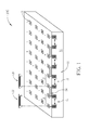
FIG. 1 is a schematic diagram depicting a solar module support according to a preferred embodiment of the present invention; -
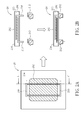
FIG. 2A shows a top view of the structure of a solar cell module according to a preferred embodiment of the present invention schematically; -
FIG. 2B shows a sectional view of the solar cell module taken along line AA' inFIG. 2A ; -
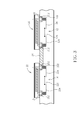
FIG. 3 is a schematic diagram depicting a turned off switching circuit when the solar cell module is engaged with the solar module support; and -
FIG. 4 is a schematic diagram ofFIG. 1 depicting a turned on switching circuit when the solar cell module is detached from the solar module support. -
FIG. 1 is a schematic diagram depicting a solar module support according to a preferred embodiment of the present invention. As shown inFIG. 1 , asolar module support 100 includes asubstrate 10. Thesubstrate 10 may be a case having a cavity within. A plurality ofswitching circuits 11 such as afirst switching circuit 12 and asecond switching circuit 14 are configured inside thesubstrate 10. The top surface or the bottom surface of thesubstrate 10 may have numerous springs disposed thereon (not shown) and posts (not shown) for routing the switching circuits. It is noteworthy that thesolar module support 100 further includes numeroussolar module sockets 15, such as a first and a secondsolar module socket substrate 10. The first and the secondsolar module sockets solar cell module 20 and a secondsolar cell module 22, respectively. Other solar module sockets are capable of fixing or installing other solar cell modules. Thefirst switching circuit 12 may be composed of resilient members and wire segments. Thesecond switching circuit 14 may have the same configuration as thefirst switching circuit 12. Aninterconnection circuit 24 is configured inside thesubstrate 10 and electrically connects the adjacent switching circuits or the adjacent solar modules. The structures of the first andsecond switching circuits solar module support 100. -
FIG. 2A shows a top view of the structure of a solar cell module according to a preferred embodiment of the present invention schematically.FIG. 2B shows a sectional view of the solar cell module taken along line AA' inFIG. 2A . - Please refer to both
FIG. 2A and FIG. 2B . The firstsolar cell module 20 includes at least onesolar cell 202. Afront sheet 204 and aback sheet 206 sandwich thesolar cell 202. Anadhesive layer 205 encapsulates thesolar cell 202. Theadhesive layer 205 can be ethylene vinyl acetate (EVA) for adhering thesolar cell 202, thefront sheet 204, and theback sheet 206. Although only onesolar cell 202 is disposed in the firstsolar cell module 20, more than one solar cell can be packaged together to become the firstsolar cell module 20. Ananode wire 210 and acathode wire 208, which serve as electrodes, extend from the surface of thesolar cell module 20 and penetrate theadhesive layer 205, and theback sheet 206. Alternatively, theanode wire 210 and thecathode wire 208 can extend from the side surface of thesolar cell module 20. Then, theanode wire 210 and thecathode wire 208 can be bent toward theback sheet 206. After that, theanode wire 210 and thecathode wire 208 are inserted intoplugs 212 respectively. Theplugs 212 are advantageously substantially perpendicular to theback sheet 206. Furthermore, theplug 212 with theanode wire 210 inside may have different features from theother plug 212 withcathode wire 208 inside. For instance, theplug 212 with theanode wire 210 inside may be blue color, and theplug 212 withcathode wire 208 inside may be green color. Theplugs 212 may be any plugs which can fix thesolar cell module 20 tightly on the solar module support. For example, the plugs may be analogous to phone plugs, Ethernet cable plugs or other types of plugs, but not limited thereto. The free ends of theplugs 212 can expose the end point of theanode wire 210 and the end point of thecathode wire 208. Although only the structure of the firstsolar cell module 20 is described, the aforesaid secondsolar cell module 22, and other solar cell modules utilized in the present invention have a structure that is identical with the firstsolar cell module 20. -
FIG. 3 is a schematic diagram depicting a turned off switching circuit when the solar cell module is engaged with the solar module support.FIG. 4 is a schematic diagram ofFIG. 1 depicting a turned on switching circuit when the solar cell module is detached from the solar module support. For the sake of simplicity, only two switching circuits are shown inFIG. 3 andFIG. 4 . However, it should be understood that all the switchingcircuits 11 on thesolar module support 100 can be operated in the same way. - Please refer to
FIGS. 1-3 . The firstsolar cell module 20 is engaged with thesubstrate 10, and the secondsolar cell module 22 is also engaged with thesubstrate 10. By plugging theplugs 212 on the firstsolar cell module 20 into the firstsolar module socket 16, theplugs 212 interlock with the firstsolar module socket 16. More particularly, the firstsolar module socket 16 has two individual recesses. Each individual recess corresponds to an anode and a cathode respectively. Theplug 212 withanode wire 210 inside should be plugged into the anode recess, and theplug 212 withcathode wire 208 inside should be plugged into the cathode recess. - When the first
solar cell module 20 is engaged with thesubstrate 10, thefirst switching circuit 12 is turned off, and no current can flow through thefirst switching circuit 12. Thefirst switching circuit 12 includes two L-shapedwire segments 124, tworesilient members 122 and abridging wire segment 126. Thesecond switching circuit 14 includes two L-shapedwire segments 224, tworesilient members 222 and abridging wire segment 226. - According to a preferred embodiment of the present invention, when the first
solar cell module 20 is plugged into the firstsolar module socket 16, theresilient members 122 of thefirst switching circuit 12 is pressed down, and two L-shapedwire segments 124 are separated from abridging wire segment 126. Thefirst switching circuit 12 is therefore turned off. At this point, the first and the secondsolar cell modules solar cell module 22 flows through the L-shapedwire segments 224,interconnection circuit 24, and the L-shapedwire segment 124 to thecathode wire 208 of the firstsolar cell module 20. Theinterconnection circuit 24 connects to the L-shapedwire segment 224 of thesecond switching circuit 14 to the L-shapedwire segment 124 of thefirst switching circuit 12. - As shown in
FIGS. 1-2 and 4 , the firstsolar cell module 20 is detached from thesubstrate 10, and the secondsolar cell module 22 is still engaged with thesubstrate 10. When the firstsolar cell module 20 is detached from thesubstrate 10, thefirst switching circuit 12 is turned on, and a current flowing from the secondsolar cell module 22 can flow through the L-shapedwire segment 224, and theinterconnection circuit 24 to thefirst switching circuit 12. When the firstsolar cell module 20 is pulled out from the firstsolar module socket 16, theresilient members 122 of thefirst switching circuit 12 spring back to their original positions, and the L-shapedwire segments 124 reconnect to thebridging wire segment 126. - Although
FIG. 3 andFIG. 4 merely describe the plug in and pull out operations of the firstsolar cell module 20 associated with thefirst switching circuit 12, thesecond switching circuit 14 is controlled in the same way as thefirst switching circuit 12. That is, when the secondsolar cell module 22 is plugged in, thesecond switching circuit 14 is turned off and when the secondsolar cell module 22 is pulled out, thesecond switching circuit 14 is turned on. Furthermore, each of thesolar module sockets 15 on thesolar module support 100 can be plugged in with one solar cell module to supply greater voltage. - The solar cell module of the present invention offers an easy way to replace a defective solar cell module. Merely by plugging in and out, the solar cell module can be engaged with the solar module support or detached from the solar module support. Furthermore, when the solar cell module is pulled out, the switching circuit corresponding to it turns on to maintain the serial circuit. Even when there is no new solar cell module to plug in for replacing the broken one, the serial circuit can still function as long as the broken solar cell module is pulled out. Moreover, since there is merely a single solar cell in one solar cell module, when the solar cell is damaged, the entire solar cell module can be replaced without peeling off the front sheet. Therefore, the expenditures of replacement of solar cell module are saved. Furthermore, the arrangement of the solar cell modules on the solar module support can be customized to form a desired pattern. For example, a symbol of a company can be pieced together by placing solar cell modules in their designated sockets.
- Those skilled in the art will readily observe that numerous modifications and alterations of the device and method may be made while retaining the teachings of the invention. All combinations and sub-combinations of the above-described features also belong to the invention.
Claims (9)
- A solar module support (100), comprising:a substrate (10); and characterized by:a first switching circuit (12) configured in the substrate (10); anda first solar module socket (16) disposed in the substrate (10) for installing a first solar cell module (20), wherein when the first solar cell module (20) is engaged with the first solar module socket (16), a first current passes through the first solar cell module (20), and when the first solar cell module (20) detaches from the first solar module socket (16), a second current passes through the first switching circuit (12).
- The solar module support (100) of claim 1, further characterized by a second switching circuit (14) configured in the substrate (10), a second solar module socket (18) disposed in the substrate (10) for installing a second solar cell module (22).
- The solar module support (100) of claim 2, characterized in that when the first solar cell module (20) is engaged with the first solar module socket (16), the first current passing through the first solar cell module (20) is provided by the second solar cell module (22) and the first solar cell module (20).
- The solar module support (100) of claim 2, characterized in that when the first solar cell module (20) detaches from the first solar module socket (16), the second current passing through the first switching circuit (12) is provided by the second solar cell module (22).
- The solar module support (100) of claim 2, further characterized by an interconnection circuit (24) configured on the substrate (10) and the interconnection circuit (24) electrically connects the first switching circuit (12) with the second solar cell module (22).
- The solar module support (100) of claim 2, further characterized by an interconnection circuit (24) configured on the substrate (10) and the interconnection circuit (24) electrically connects the first solar cell module (20) with the second solar cell module (22).
- The solar module support (100) of claim 1, characterized in that the first solar cell module (20) further comprises two plugs (212), and the plugs (212) are capable of plugging into the first solar module socket (16) so as to interlock the first solar cell module (20) on the substrate (10).
- The solar module support (100) of claim 1, characterized in that when the first solar cell module (20) is engaged with the first solar module socket (16), the first switching circuit (12) is turned off, and when the first solar cell module (20) is detached from the first solar module socket (16), the first switching circuit (12) is turned on.
- A solar cell module (20) that is fixable on the solar module support (100) of Claim 1, comprising:a back sheet (206);a front sheet (204) disposed on the back sheet (206);at least one solar cell (202) disposed between the front sheet (204) and the back sheet (206); andan adhesive layer (205) encapsulating the at least one solar cell (202); and characterized by:an anode wire (208) penetrating the adhesive layer (205) and the back sheet (206);a cathode wire (210) penetrating the adhesive layer (205) and the back sheet (206); andtwo plugs (212) that are fixable on the solar module support (100);wherein the anode wire (208) is inserted into one plug (212) and the cathode wire (210) is inserted into the other plug (212).
Applications Claiming Priority (1)
| Application Number | Priority Date | Filing Date | Title |
|---|---|---|---|
| TW099118571A TWI433325B (en) | 2010-06-08 | 2010-06-08 | Solar module support board |
Publications (3)
| Publication Number | Publication Date |
|---|---|
| EP2395555A2 true EP2395555A2 (en) | 2011-12-14 |
| EP2395555A3 EP2395555A3 (en) | 2015-10-28 |
| EP2395555B1 EP2395555B1 (en) | 2021-03-10 |
Family
ID=44718925
Family Applications (1)
| Application Number | Title | Priority Date | Filing Date |
|---|---|---|---|
| EP10190605.5A Active EP2395555B1 (en) | 2010-06-08 | 2010-11-10 | Solar module support and solar cell module |
Country Status (2)
| Country | Link |
|---|---|
| EP (1) | EP2395555B1 (en) |
| TW (1) | TWI433325B (en) |
Cited By (3)
| Publication number | Priority date | Publication date | Assignee | Title |
|---|---|---|---|---|
| US10505492B2 (en) | 2016-02-12 | 2019-12-10 | Solarcity Corporation | Building integrated photovoltaic roofing assemblies and associated systems and methods |
| EP3639364A1 (en) * | 2017-06-15 | 2020-04-22 | Grafmarine | Power distribution and cell storage apparatus |
| EP3700083A1 (en) * | 2019-02-20 | 2020-08-26 | SunPower Corporation | Aggregated photovoltaic panels |
Family Cites Families (2)
| Publication number | Priority date | Publication date | Assignee | Title |
|---|---|---|---|---|
| JPH11150287A (en) * | 1997-09-10 | 1999-06-02 | Canon Inc | Solar cell module, enclosure with solar cell, method of installing enclosure with solar cell, and solar power generation system |
| EP2232577A1 (en) * | 2007-12-18 | 2010-09-29 | Day4 Energy Inc. | Photovoltaic module with edge access to pv strings, interconnection method, apparatus, and system |
-
2010
- 2010-06-08 TW TW099118571A patent/TWI433325B/en active
- 2010-11-10 EP EP10190605.5A patent/EP2395555B1/en active Active
Non-Patent Citations (1)
| Title |
|---|
| None |
Cited By (9)
| Publication number | Priority date | Publication date | Assignee | Title |
|---|---|---|---|---|
| US10505492B2 (en) | 2016-02-12 | 2019-12-10 | Solarcity Corporation | Building integrated photovoltaic roofing assemblies and associated systems and methods |
| EP3639364A1 (en) * | 2017-06-15 | 2020-04-22 | Grafmarine | Power distribution and cell storage apparatus |
| EP4383358A3 (en) * | 2017-06-15 | 2024-12-18 | Grafmarine | Power distribution |
| US12199205B2 (en) | 2017-06-15 | 2025-01-14 | Grafmarine Limited | Power distribution and cell storage apparatus |
| EP3700083A1 (en) * | 2019-02-20 | 2020-08-26 | SunPower Corporation | Aggregated photovoltaic panels |
| US11527990B2 (en) | 2019-02-20 | 2022-12-13 | Sunpower Corporation | Aggregated photovoltaic panels |
| US20230086161A1 (en) * | 2019-02-20 | 2023-03-23 | Sunpower Corporation | Aggregated photovoltaic panels |
| EP4236062A2 (en) | 2019-02-20 | 2023-08-30 | Maxeon Solar Pte. Ltd. | Aggregated photovoltaic panels |
| EP4236062A3 (en) * | 2019-02-20 | 2023-09-13 | Maxeon Solar Pte. Ltd. | Aggregated photovoltaic panels |
Also Published As
| Publication number | Publication date |
|---|---|
| EP2395555A3 (en) | 2015-10-28 |
| TW201145529A (en) | 2011-12-16 |
| EP2395555B1 (en) | 2021-03-10 |
| TWI433325B (en) | 2014-04-01 |
Similar Documents
| Publication | Publication Date | Title |
|---|---|---|
| CN105359371B (en) | Solar cell module | |
| US8558102B2 (en) | Rotatable junction box for a solar module | |
| JP6357102B2 (en) | Smart photovoltaic cells and modules | |
| CN109768095B (en) | Overlapping type solar cell module | |
| US20160172510A1 (en) | Photovoltaic module | |
| CN105336749B (en) | Upside-down mounting multijunction solar cell chip of integrated bypass diode and preparation method thereof | |
| KR20100097219A (en) | Photovoltaic module with edge access to pv strings, interconnection method, apparatus, and system | |
| CN102217087A (en) | Integrated bypass diode assemblies for back contact solar cells and modules | |
| US20170170336A1 (en) | Systems and methods for routing wires in a solar module | |
| CN105097975A (en) | Solar battery assembly | |
| JP2013518423A (en) | Solar module array and diode cable | |
| WO2021201342A1 (en) | Designable shingled photovoltaic module and manufacturing method therefor | |
| JP2018518934A (en) | General purpose photovoltaic laminate | |
| JP2015065276A (en) | Photoelectric conversion device | |
| JP6595866B2 (en) | Photovoltaic power generation system and method of using the same | |
| EP2395555B1 (en) | Solar module support and solar cell module | |
| KR20180079425A (en) | Back electrode type solar cell substrate, method for manufacturing the same, and back electrode type solar cell | |
| US12328953B2 (en) | Solar cell module | |
| US20110303285A1 (en) | Solar module support and solar cell module | |
| JP2011096968A (en) | Solar generator for individually performing maximum power point tracking, and solar cell of the same | |
| GB2564123A (en) | Multi-purpose off-grid PV module design | |
| US12610628B2 (en) | Solar-cell module | |
| CN104660167A (en) | EL testing method for photovoltaic module provided with power optimizer | |
| JP2007042767A (en) | Solar power plant | |
| CN102544129A (en) | Solar battery |
Legal Events
| Date | Code | Title | Description |
|---|---|---|---|
| AK | Designated contracting states |
Kind code of ref document: A2 Designated state(s): AL AT BE BG CH CY CZ DE DK EE ES FI FR GB GR HR HU IE IS IT LI LT LU LV MC MK MT NL NO PL PT RO RS SE SI SK SM TR |
|
| AX | Request for extension of the european patent |
Extension state: BA ME |
|
| PUAI | Public reference made under article 153(3) epc to a published international application that has entered the european phase |
Free format text: ORIGINAL CODE: 0009012 |
|
| RAP1 | Party data changed (applicant data changed or rights of an application transferred) |
Owner name: NEO SOLAR POWER CORP. |
|
| PUAL | Search report despatched |
Free format text: ORIGINAL CODE: 0009013 |
|
| AK | Designated contracting states |
Kind code of ref document: A3 Designated state(s): AL AT BE BG CH CY CZ DE DK EE ES FI FR GB GR HR HU IE IS IT LI LT LU LV MC MK MT NL NO PL PT RO RS SE SI SK SM TR |
|
| AX | Request for extension of the european patent |
Extension state: BA ME |
|
| RIC1 | Information provided on ipc code assigned before grant |
Ipc: H01L 31/042 20140101AFI20150925BHEP Ipc: H01L 31/05 20140101ALI20150925BHEP |
|
| 17P | Request for examination filed |
Effective date: 20160427 |
|
| RBV | Designated contracting states (corrected) |
Designated state(s): AL AT BE BG CH CY CZ DE DK EE ES FI FR GB GR HR HU IE IS IT LI LT LU LV MC MK MT NL NO PL PT RO RS SE SI SK SM TR |
|
| STAA | Information on the status of an ep patent application or granted ep patent |
Free format text: STATUS: EXAMINATION IS IN PROGRESS |
|
| 17Q | First examination report despatched |
Effective date: 20180830 |
|
| RIC1 | Information provided on ipc code assigned before grant |
Ipc: H02S 40/34 20140101ALI20190716BHEP Ipc: H01L 31/05 20140101ALI20190716BHEP Ipc: H01L 31/042 20140101AFI20190716BHEP |
|
| REG | Reference to a national code |
Ref country code: DE Ref legal event code: R079 Ref document number: 602010066565 Country of ref document: DE Free format text: PREVIOUS MAIN CLASS: H01L0031042000 Ipc: H01L0031020000 |
|
| RIC1 | Information provided on ipc code assigned before grant |
Ipc: H02S 40/34 20140101ALI20191211BHEP Ipc: H02S 40/36 20140101ALI20191211BHEP Ipc: H02S 20/00 20140101ALI20191211BHEP Ipc: H01L 31/05 20140101ALI20191211BHEP Ipc: H01L 31/02 20060101AFI20191211BHEP |
|
| GRAP | Despatch of communication of intention to grant a patent |
Free format text: ORIGINAL CODE: EPIDOSNIGR1 |
|
| STAA | Information on the status of an ep patent application or granted ep patent |
Free format text: STATUS: GRANT OF PATENT IS INTENDED |
|
| INTG | Intention to grant announced |
Effective date: 20200721 |
|
| GRAS | Grant fee paid |
Free format text: ORIGINAL CODE: EPIDOSNIGR3 |
|
| GRAA | (expected) grant |
Free format text: ORIGINAL CODE: 0009210 |
|
| STAA | Information on the status of an ep patent application or granted ep patent |
Free format text: STATUS: THE PATENT HAS BEEN GRANTED |
|
| RAP1 | Party data changed (applicant data changed or rights of an application transferred) |
Owner name: UNITED RENEWABLE ENERGY CO., LTD. |
|
| AK | Designated contracting states |
Kind code of ref document: B1 Designated state(s): AL AT BE BG CH CY CZ DE DK EE ES FI FR GB GR HR HU IE IS IT LI LT LU LV MC MK MT NL NO PL PT RO RS SE SI SK SM TR |
|
| REG | Reference to a national code |
Ref country code: GB Ref legal event code: FG4D |
|
| REG | Reference to a national code |
Ref country code: AT Ref legal event code: REF Ref document number: 1370770 Country of ref document: AT Kind code of ref document: T Effective date: 20210315 Ref country code: CH Ref legal event code: EP |
|
| REG | Reference to a national code |
Ref country code: IE Ref legal event code: FG4D |
|
| REG | Reference to a national code |
Ref country code: DE Ref legal event code: R096 Ref document number: 602010066565 Country of ref document: DE |
|
| REG | Reference to a national code |
Ref country code: LT Ref legal event code: MG9D |
|
| PG25 | Lapsed in a contracting state [announced via postgrant information from national office to epo] |
Ref country code: FI Free format text: LAPSE BECAUSE OF FAILURE TO SUBMIT A TRANSLATION OF THE DESCRIPTION OR TO PAY THE FEE WITHIN THE PRESCRIBED TIME-LIMIT Effective date: 20210310 Ref country code: GR Free format text: LAPSE BECAUSE OF FAILURE TO SUBMIT A TRANSLATION OF THE DESCRIPTION OR TO PAY THE FEE WITHIN THE PRESCRIBED TIME-LIMIT Effective date: 20210611 Ref country code: HR Free format text: LAPSE BECAUSE OF FAILURE TO SUBMIT A TRANSLATION OF THE DESCRIPTION OR TO PAY THE FEE WITHIN THE PRESCRIBED TIME-LIMIT Effective date: 20210310 Ref country code: LT Free format text: LAPSE BECAUSE OF FAILURE TO SUBMIT A TRANSLATION OF THE DESCRIPTION OR TO PAY THE FEE WITHIN THE PRESCRIBED TIME-LIMIT Effective date: 20210310 Ref country code: BG Free format text: LAPSE BECAUSE OF FAILURE TO SUBMIT A TRANSLATION OF THE DESCRIPTION OR TO PAY THE FEE WITHIN THE PRESCRIBED TIME-LIMIT Effective date: 20210610 Ref country code: NO Free format text: LAPSE BECAUSE OF FAILURE TO SUBMIT A TRANSLATION OF THE DESCRIPTION OR TO PAY THE FEE WITHIN THE PRESCRIBED TIME-LIMIT Effective date: 20210610 |
|
| REG | Reference to a national code |
Ref country code: AT Ref legal event code: MK05 Ref document number: 1370770 Country of ref document: AT Kind code of ref document: T Effective date: 20210310 |
|
| REG | Reference to a national code |
Ref country code: NL Ref legal event code: MP Effective date: 20210310 |
|
| PG25 | Lapsed in a contracting state [announced via postgrant information from national office to epo] |
Ref country code: SE Free format text: LAPSE BECAUSE OF FAILURE TO SUBMIT A TRANSLATION OF THE DESCRIPTION OR TO PAY THE FEE WITHIN THE PRESCRIBED TIME-LIMIT Effective date: 20210310 Ref country code: RS Free format text: LAPSE BECAUSE OF FAILURE TO SUBMIT A TRANSLATION OF THE DESCRIPTION OR TO PAY THE FEE WITHIN THE PRESCRIBED TIME-LIMIT Effective date: 20210310 Ref country code: LV Free format text: LAPSE BECAUSE OF FAILURE TO SUBMIT A TRANSLATION OF THE DESCRIPTION OR TO PAY THE FEE WITHIN THE PRESCRIBED TIME-LIMIT Effective date: 20210310 |
|
| PG25 | Lapsed in a contracting state [announced via postgrant information from national office to epo] |
Ref country code: NL Free format text: LAPSE BECAUSE OF FAILURE TO SUBMIT A TRANSLATION OF THE DESCRIPTION OR TO PAY THE FEE WITHIN THE PRESCRIBED TIME-LIMIT Effective date: 20210310 |
|
| PG25 | Lapsed in a contracting state [announced via postgrant information from national office to epo] |
Ref country code: SM Free format text: LAPSE BECAUSE OF FAILURE TO SUBMIT A TRANSLATION OF THE DESCRIPTION OR TO PAY THE FEE WITHIN THE PRESCRIBED TIME-LIMIT Effective date: 20210310 Ref country code: AT Free format text: LAPSE BECAUSE OF FAILURE TO SUBMIT A TRANSLATION OF THE DESCRIPTION OR TO PAY THE FEE WITHIN THE PRESCRIBED TIME-LIMIT Effective date: 20210310 Ref country code: EE Free format text: LAPSE BECAUSE OF FAILURE TO SUBMIT A TRANSLATION OF THE DESCRIPTION OR TO PAY THE FEE WITHIN THE PRESCRIBED TIME-LIMIT Effective date: 20210310 Ref country code: CZ Free format text: LAPSE BECAUSE OF FAILURE TO SUBMIT A TRANSLATION OF THE DESCRIPTION OR TO PAY THE FEE WITHIN THE PRESCRIBED TIME-LIMIT Effective date: 20210310 |
|
| PG25 | Lapsed in a contracting state [announced via postgrant information from national office to epo] |
Ref country code: IS Free format text: LAPSE BECAUSE OF FAILURE TO SUBMIT A TRANSLATION OF THE DESCRIPTION OR TO PAY THE FEE WITHIN THE PRESCRIBED TIME-LIMIT Effective date: 20210710 Ref country code: RO Free format text: LAPSE BECAUSE OF FAILURE TO SUBMIT A TRANSLATION OF THE DESCRIPTION OR TO PAY THE FEE WITHIN THE PRESCRIBED TIME-LIMIT Effective date: 20210310 Ref country code: PL Free format text: LAPSE BECAUSE OF FAILURE TO SUBMIT A TRANSLATION OF THE DESCRIPTION OR TO PAY THE FEE WITHIN THE PRESCRIBED TIME-LIMIT Effective date: 20210310 Ref country code: PT Free format text: LAPSE BECAUSE OF FAILURE TO SUBMIT A TRANSLATION OF THE DESCRIPTION OR TO PAY THE FEE WITHIN THE PRESCRIBED TIME-LIMIT Effective date: 20210712 Ref country code: SK Free format text: LAPSE BECAUSE OF FAILURE TO SUBMIT A TRANSLATION OF THE DESCRIPTION OR TO PAY THE FEE WITHIN THE PRESCRIBED TIME-LIMIT Effective date: 20210310 Ref country code: ES Free format text: LAPSE BECAUSE OF FAILURE TO SUBMIT A TRANSLATION OF THE DESCRIPTION OR TO PAY THE FEE WITHIN THE PRESCRIBED TIME-LIMIT Effective date: 20210310 |
|
| REG | Reference to a national code |
Ref country code: DE Ref legal event code: R097 Ref document number: 602010066565 Country of ref document: DE |
|
| PLBE | No opposition filed within time limit |
Free format text: ORIGINAL CODE: 0009261 |
|
| STAA | Information on the status of an ep patent application or granted ep patent |
Free format text: STATUS: NO OPPOSITION FILED WITHIN TIME LIMIT |
|
| PG25 | Lapsed in a contracting state [announced via postgrant information from national office to epo] |
Ref country code: DK Free format text: LAPSE BECAUSE OF FAILURE TO SUBMIT A TRANSLATION OF THE DESCRIPTION OR TO PAY THE FEE WITHIN THE PRESCRIBED TIME-LIMIT Effective date: 20210310 Ref country code: AL Free format text: LAPSE BECAUSE OF FAILURE TO SUBMIT A TRANSLATION OF THE DESCRIPTION OR TO PAY THE FEE WITHIN THE PRESCRIBED TIME-LIMIT Effective date: 20210310 |
|
| 26N | No opposition filed |
Effective date: 20211213 |
|
| PG25 | Lapsed in a contracting state [announced via postgrant information from national office to epo] |
Ref country code: SI Free format text: LAPSE BECAUSE OF FAILURE TO SUBMIT A TRANSLATION OF THE DESCRIPTION OR TO PAY THE FEE WITHIN THE PRESCRIBED TIME-LIMIT Effective date: 20210310 |
|
| PG25 | Lapsed in a contracting state [announced via postgrant information from national office to epo] |
Ref country code: IT Free format text: LAPSE BECAUSE OF FAILURE TO SUBMIT A TRANSLATION OF THE DESCRIPTION OR TO PAY THE FEE WITHIN THE PRESCRIBED TIME-LIMIT Effective date: 20210310 |
|
| PG25 | Lapsed in a contracting state [announced via postgrant information from national office to epo] |
Ref country code: IS Free format text: LAPSE BECAUSE OF FAILURE TO SUBMIT A TRANSLATION OF THE DESCRIPTION OR TO PAY THE FEE WITHIN THE PRESCRIBED TIME-LIMIT Effective date: 20210710 |
|
| PG25 | Lapsed in a contracting state [announced via postgrant information from national office to epo] |
Ref country code: MC Free format text: LAPSE BECAUSE OF FAILURE TO SUBMIT A TRANSLATION OF THE DESCRIPTION OR TO PAY THE FEE WITHIN THE PRESCRIBED TIME-LIMIT Effective date: 20210310 |
|
| REG | Reference to a national code |
Ref country code: CH Ref legal event code: PL |
|
| GBPC | Gb: european patent ceased through non-payment of renewal fee |
Effective date: 20211110 |
|
| PG25 | Lapsed in a contracting state [announced via postgrant information from national office to epo] |
Ref country code: LU Free format text: LAPSE BECAUSE OF NON-PAYMENT OF DUE FEES Effective date: 20211110 Ref country code: BE Free format text: LAPSE BECAUSE OF NON-PAYMENT OF DUE FEES Effective date: 20211130 |
|
| REG | Reference to a national code |
Ref country code: BE Ref legal event code: MM Effective date: 20211130 |
|
| PG25 | Lapsed in a contracting state [announced via postgrant information from national office to epo] |
Ref country code: LI Free format text: LAPSE BECAUSE OF NON-PAYMENT OF DUE FEES Effective date: 20211130 Ref country code: CH Free format text: LAPSE BECAUSE OF NON-PAYMENT OF DUE FEES Effective date: 20211130 |
|
| PG25 | Lapsed in a contracting state [announced via postgrant information from national office to epo] |
Ref country code: IE Free format text: LAPSE BECAUSE OF NON-PAYMENT OF DUE FEES Effective date: 20211110 Ref country code: GB Free format text: LAPSE BECAUSE OF NON-PAYMENT OF DUE FEES Effective date: 20211110 |
|
| PG25 | Lapsed in a contracting state [announced via postgrant information from national office to epo] |
Ref country code: FR Free format text: LAPSE BECAUSE OF NON-PAYMENT OF DUE FEES Effective date: 20211130 |
|
| PG25 | Lapsed in a contracting state [announced via postgrant information from national office to epo] |
Ref country code: HU Free format text: LAPSE BECAUSE OF FAILURE TO SUBMIT A TRANSLATION OF THE DESCRIPTION OR TO PAY THE FEE WITHIN THE PRESCRIBED TIME-LIMIT; INVALID AB INITIO Effective date: 20101110 Ref country code: CY Free format text: LAPSE BECAUSE OF FAILURE TO SUBMIT A TRANSLATION OF THE DESCRIPTION OR TO PAY THE FEE WITHIN THE PRESCRIBED TIME-LIMIT Effective date: 20210310 |
|
| PG25 | Lapsed in a contracting state [announced via postgrant information from national office to epo] |
Ref country code: MK Free format text: LAPSE BECAUSE OF FAILURE TO SUBMIT A TRANSLATION OF THE DESCRIPTION OR TO PAY THE FEE WITHIN THE PRESCRIBED TIME-LIMIT Effective date: 20210310 |
|
| REG | Reference to a national code |
Ref country code: DE Ref legal event code: R082 Ref document number: 602010066565 Country of ref document: DE Representative=s name: STRAUS, ALEXANDER, DIPL.-CHEM.UNIV. DR.PHIL., DE |
|
| PG25 | Lapsed in a contracting state [announced via postgrant information from national office to epo] |
Ref country code: MT Free format text: LAPSE BECAUSE OF FAILURE TO SUBMIT A TRANSLATION OF THE DESCRIPTION OR TO PAY THE FEE WITHIN THE PRESCRIBED TIME-LIMIT Effective date: 20210310 |
|
| REG | Reference to a national code |
Ref country code: DE Ref legal event code: R079 Ref document number: 602010066565 Country of ref document: DE Free format text: PREVIOUS MAIN CLASS: H01L0031020000 Ipc: H10F0077000000 |
|
| PG25 | Lapsed in a contracting state [announced via postgrant information from national office to epo] |
Ref country code: TR Free format text: LAPSE BECAUSE OF FAILURE TO SUBMIT A TRANSLATION OF THE DESCRIPTION OR TO PAY THE FEE WITHIN THE PRESCRIBED TIME-LIMIT Effective date: 20210310 |
|
| PGFP | Annual fee paid to national office [announced via postgrant information from national office to epo] |
Ref country code: DE Payment date: 20251129 Year of fee payment: 16 |