EP2393282A1 - Solid-state imaging device - Google Patents
Solid-state imaging device Download PDFInfo
- Publication number
- EP2393282A1 EP2393282A1 EP10735746A EP10735746A EP2393282A1 EP 2393282 A1 EP2393282 A1 EP 2393282A1 EP 10735746 A EP10735746 A EP 10735746A EP 10735746 A EP10735746 A EP 10735746A EP 2393282 A1 EP2393282 A1 EP 2393282A1
- Authority
- EP
- European Patent Office
- Prior art keywords
- solid
- imaging device
- state imaging
- units
- charge
- Prior art date
- Legal status (The legal status is an assumption and is not a legal conclusion. Google has not performed a legal analysis and makes no representation as to the accuracy of the status listed.)
- Ceased
Links
Images
Classifications
-
- H—ELECTRICITY
- H10—SEMICONDUCTOR DEVICES; ELECTRIC SOLID-STATE DEVICES NOT OTHERWISE PROVIDED FOR
- H10F—INORGANIC SEMICONDUCTOR DEVICES SENSITIVE TO INFRARED RADIATION, LIGHT, ELECTROMAGNETIC RADIATION OF SHORTER WAVELENGTH OR CORPUSCULAR RADIATION
- H10F39/00—Integrated devices, or assemblies of multiple devices, comprising at least one element covered by group H10F30/00, e.g. radiation detectors comprising photodiode arrays
- H10F39/80—Constructional details of image sensors
- H10F39/803—Pixels having integrated switching, control, storage or amplification elements
-
- H—ELECTRICITY
- H04—ELECTRIC COMMUNICATION TECHNIQUE
- H04N—PICTORIAL COMMUNICATION, e.g. TELEVISION
- H04N25/00—Circuitry of solid-state image sensors [SSIS]; Control thereof
- H04N25/70—SSIS architectures; Circuits associated therewith
- H04N25/71—Charge-coupled device [CCD] sensors; Charge-transfer registers specially adapted for CCD sensors
-
- H—ELECTRICITY
- H10—SEMICONDUCTOR DEVICES; ELECTRIC SOLID-STATE DEVICES NOT OTHERWISE PROVIDED FOR
- H10F—INORGANIC SEMICONDUCTOR DEVICES SENSITIVE TO INFRARED RADIATION, LIGHT, ELECTROMAGNETIC RADIATION OF SHORTER WAVELENGTH OR CORPUSCULAR RADIATION
- H10F39/00—Integrated devices, or assemblies of multiple devices, comprising at least one element covered by group H10F30/00, e.g. radiation detectors comprising photodiode arrays
- H10F39/80—Constructional details of image sensors
-
- H—ELECTRICITY
- H10—SEMICONDUCTOR DEVICES; ELECTRIC SOLID-STATE DEVICES NOT OTHERWISE PROVIDED FOR
- H10D—INORGANIC ELECTRIC SEMICONDUCTOR DEVICES
- H10D44/00—Charge transfer devices
- H10D44/40—Charge-coupled devices [CCD]
- H10D44/45—Charge-coupled devices [CCD] having field effect produced by insulated gate electrodes
- H10D44/454—Output structures
-
- H—ELECTRICITY
- H10—SEMICONDUCTOR DEVICES; ELECTRIC SOLID-STATE DEVICES NOT OTHERWISE PROVIDED FOR
- H10F—INORGANIC SEMICONDUCTOR DEVICES SENSITIVE TO INFRARED RADIATION, LIGHT, ELECTROMAGNETIC RADIATION OF SHORTER WAVELENGTH OR CORPUSCULAR RADIATION
- H10F39/00—Integrated devices, or assemblies of multiple devices, comprising at least one element covered by group H10F30/00, e.g. radiation detectors comprising photodiode arrays
- H10F39/10—Integrated devices
- H10F39/12—Image sensors
- H10F39/15—Charge-coupled device [CCD] image sensors
Definitions
- the present invention relates to a multi-port type and charge multiplying type of solid-state imaging device.
- Such solid-state imaging devices include an imaging region and a plurality of units.
- the imaging region includes a plurality of pixel columns.
- Each of the units has an output register that transfers a charge from one or more corresponding pixel columns out of the pixel columns, a multiplication register that receives the charge transferred by the output register to generate a multiplied charge, and an amplifier that generates a signal based on the multiplied charge from the multiplication register.
- a solid-state imaging device of the present invention is a multi-port solid-state imaging device, and includes an imaging region and a plurality of units.
- the imaging region includes a plurality of pixel columns.
- the units generate signals based on charges from the imaging region.
- Each of the units has an output register, a plurality of multiplication registers, and an amplifier.
- the output register transfers a charge from one or more corresponding pixel columns out of the plurality of pixel columns.
- the multiplication registers are arranged in parallel, and receive the charge from the output register to generate multiplied charges individually.
- the amplifier generates a signal based on the multiplied charges from the multiplication registers.
- each of the units forming multiple ports has a plurality of multiplication registers provided in parallel, even if there is a variation in gain among the multiplication registers, the gain of each unit is averaged. Consequently, the variation in gain among the units is reduced.
- a multi-port and charge multiplying solid-state imaging device that outputs from a plurality of units signals based on charges from an imaging region, and that is capable of reducing variation in gain among the units is provided.
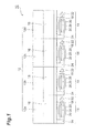
- Fig. 1 is a view showing a solid-state imaging device according to an embodiment.
- Fig. 1 is a view showing a solid-state imaging device according to an embodiment.
- the solid-state imaging device 10 shown in Fig. 1 includes an imaging region 12, and a plurality of units 14.
- the imaging region 12 is a region that generates charges in response to incident light.
- the imaging region 12 includes a plurality of pixels arrayed two-dimensionally, and each pixel includes a photodiode.
- the solid-state imaging device 10 of the present embodiment includes charge accumulating regions 16 as well as the imaging region 12.
- the charge accumulating region 16 is a section that temporarily accumulates charges generated by the imaging region 12 before transferring the charges to output registers described later.
- the solid-state imaging device 10 having such charge accumulating regions 16 is called a frame transfer CCD image sensor.
- the solid-state imaging device of the present invention may be an interline CCD image sensor or a full-frame transfer CCD image sensor.
- the imaging region 12 has a plurality of areas 12a to 12d.
- the areas 12a to 12d are arranged in the horizontal direction, and a plurality of pixel columns are included in each area. Charges generated by the areas 12a to 12d are output to corresponding units 14.
- the imaging region 12 of the solid-state imaging device 10 contains four areas, that is, the solid-state imaging device 10 is a 4-port solid-state imaging device. However, the number of ports of the solid-state imaging device of the present invention is not limited to four.
- Each of the units 14 has an output register 18, a plurality of multiplication registers 20, and an amplifier 22.
- each of the units 14 further may include a corner register 24.
- the output register 18 is a transfer register that receives a charge generated by a corresponding area of the imaging region 12 and then transferred in the vertical direction to transfer the charge in the horizontal direction.
- the corner register 24 is a transfer register that transfers a charge like the output register 18. The corner register 24 is provided between the output register 18 and the multiplication register 20. The corner register 24 transfers a charge transferred by the output register 18 to the multiplication register 20.
- the multiplication registers 20 are each a register that multiplies a charge by an impact ionization effect, and transfers the multiplied charge.
- each unit has three multiplication registers.
- each unit may have two or more multiplication registers.
- the multiplication registers 20 are provided in parallel between the output register 18 and the amplifier 22. These multiplication registers 20 receive via the corner register 24 a charge transferred from the output register 18, and output multiplied charges to the amplifier 22.
- the amplifier 22 receives charges multiplied by the multiplication registers 20 to perform charge-voltage conversion, and generates a signal according to the amount of the received charges.
- a floating diffusion amplifier may be used as the amplifier 22.
- a signal based on charges multiplied by the multiplication registers 20 provided in parallel are output from the amplifier 22. Therefore, even if the multiplication registers 20 have variation in their gains, the gain of each unit 14 is averaged. Consequently, the variation in gain among the units 14 is reduced. Hence, images to be obtained by the solid state-imaging device 10 are high quality.
Landscapes
- Engineering & Computer Science (AREA)
- Multimedia (AREA)
- Signal Processing (AREA)
- Solid State Image Pick-Up Elements (AREA)
- Transforming Light Signals Into Electric Signals (AREA)
- Studio Devices (AREA)
Abstract
Description
- The present invention relates to a multi-port type and charge multiplying type of solid-state imaging device.
- Among solid-state imaging devices, there are multi-port and charge multiplying solid-state imaging devices as described in Japanese Patent Laid-Open No.
2007-124675 3862850 -
- Patent Literature 1: Japanese Patent Laid-Open No.
2007-124675 - Patent Literature 2: Japanese Patent No.
3862850 - It is desired for a multi-port and charge multiplying solid-state imaging devices to reduce variation in gain of multiplication registers in all units. However, it has been generally difficult due to various factors such as production tolerances to suppress variation in gain among the units.
- It is an object of the present invention to provide a multi-port and charge multiplying solid-state imaging device that outputs from a plurality of units signals based on charges from an imaging region, and that is capable of reducing variation in gain among the units.
- A solid-state imaging device of the present invention is a multi-port solid-state imaging device, and includes an imaging region and a plurality of units. The imaging region includes a plurality of pixel columns. The units generate signals based on charges from the imaging region. Each of the units has an output register, a plurality of multiplication registers, and an amplifier. The output register transfers a charge from one or more corresponding pixel columns out of the plurality of pixel columns. The multiplication registers are arranged in parallel, and receive the charge from the output register to generate multiplied charges individually. The amplifier generates a signal based on the multiplied charges from the multiplication registers.
- According to this solid-state imaging device, since each of the units forming multiple ports has a plurality of multiplication registers provided in parallel, even if there is a variation in gain among the multiplication registers, the gain of each unit is averaged. Consequently, the variation in gain among the units is reduced.
- As has been described above, according to the present invention, a multi-port and charge multiplying solid-state imaging device that outputs from a plurality of units signals based on charges from an imaging region, and that is capable of reducing variation in gain among the units is provided.
-
Fig. 1 is a view showing a solid-state imaging device according to an embodiment. - Hereinafter, a preferred embodiment of the present invention will be described in detail with reference to the drawings.
-
Fig. 1 is a view showing a solid-state imaging device according to an embodiment. The solid-state imaging device 10 shown inFig. 1 includes animaging region 12, and a plurality ofunits 14. - The
imaging region 12 is a region that generates charges in response to incident light. Specifically, theimaging region 12 includes a plurality of pixels arrayed two-dimensionally, and each pixel includes a photodiode. - The solid-
state imaging device 10 of the present embodiment includescharge accumulating regions 16 as well as theimaging region 12. Thecharge accumulating region 16 is a section that temporarily accumulates charges generated by theimaging region 12 before transferring the charges to output registers described later. The solid-state imaging device 10 having suchcharge accumulating regions 16 is called a frame transfer CCD image sensor. However, the solid-state imaging device of the present invention may be an interline CCD image sensor or a full-frame transfer CCD image sensor. - The
imaging region 12 has a plurality ofareas 12a to 12d. Theareas 12a to 12d are arranged in the horizontal direction, and a plurality of pixel columns are included in each area. Charges generated by theareas 12a to 12d are output tocorresponding units 14. In addition, theimaging region 12 of the solid-state imaging device 10 contains four areas, that is, the solid-state imaging device 10 is a 4-port solid-state imaging device. However, the number of ports of the solid-state imaging device of the present invention is not limited to four. - Each of the
units 14 has anoutput register 18, a plurality ofmultiplication registers 20, and anamplifier 22. In the present embodiment, each of theunits 14 further may include acorner register 24. - The
output register 18 is a transfer register that receives a charge generated by a corresponding area of theimaging region 12 and then transferred in the vertical direction to transfer the charge in the horizontal direction. Thecorner register 24 is a transfer register that transfers a charge like theoutput register 18. Thecorner register 24 is provided between theoutput register 18 and themultiplication register 20. Thecorner register 24 transfers a charge transferred by theoutput register 18 to themultiplication register 20. - The
multiplication registers 20 are each a register that multiplies a charge by an impact ionization effect, and transfers the multiplied charge. In the present embodiment, each unit has three multiplication registers. However, in the solid-state imaging device of the present invention, each unit may have two or more multiplication registers. - In the solid-
state imaging device 10, themultiplication registers 20 are provided in parallel between theoutput register 18 and theamplifier 22. Thesemultiplication registers 20 receive via the corner register 24 a charge transferred from theoutput register 18, and output multiplied charges to theamplifier 22. - The
amplifier 22 receives charges multiplied by themultiplication registers 20 to perform charge-voltage conversion, and generates a signal according to the amount of the received charges. As theamplifier 22, a floating diffusion amplifier may be used. - According to the solid-
state imaging device 10 described above, a signal based on charges multiplied by themultiplication registers 20 provided in parallel are output from theamplifier 22. Therefore, even if themultiplication registers 20 have variation in their gains, the gain of eachunit 14 is averaged. Consequently, the variation in gain among theunits 14 is reduced. Hence, images to be obtained by the solid state-imaging device 10 are high quality. - 10 ... Solid-state image imaging device, 12 ... Imaging region, 14 ... Unit, 16 ... Charge accumulating region, 18 ... Output register, 20 ... Multiplication register, 22 ... Amplifier, 24 ... Corner register.
Claims (1)
- A multi-port solid-state imaging device comprising:an imaging region including a plurality of pixel columns; anda plurality of units that generate signals based on charges from the imaging region,each of the units having:an output register that transfers a charge from one or more corresponding pixel columns out of the plurality of pixel columns;a plurality of multiplication registers that receive the charge from the output register to generate multiplied charges individually, the multiplication registers being arranged in parallel; andan amplifier that generates a signal based on the multiplied charges from the plurality of multiplication registers.
Applications Claiming Priority (2)
| Application Number | Priority Date | Filing Date | Title |
|---|---|---|---|
| JP2009020465A JP5346605B2 (en) | 2009-01-30 | 2009-01-30 | Solid-state imaging device |
| PCT/JP2010/050776 WO2010087277A1 (en) | 2009-01-30 | 2010-01-22 | Solid-state imaging device |
Publications (2)
| Publication Number | Publication Date |
|---|---|
| EP2393282A1 true EP2393282A1 (en) | 2011-12-07 |
| EP2393282A4 EP2393282A4 (en) | 2012-09-19 |
Family
ID=42395539
Family Applications (1)
| Application Number | Title | Priority Date | Filing Date |
|---|---|---|---|
| EP10735746A Ceased EP2393282A4 (en) | 2009-01-30 | 2010-01-22 | SEMICONDUCTOR IMAGING DEVICE |
Country Status (7)
| Country | Link |
|---|---|
| US (1) | US8520111B2 (en) |
| EP (1) | EP2393282A4 (en) |
| JP (1) | JP5346605B2 (en) |
| KR (1) | KR101594201B1 (en) |
| CN (1) | CN102246508B (en) |
| TW (1) | TWI531235B (en) |
| WO (1) | WO2010087277A1 (en) |
Families Citing this family (2)
| Publication number | Priority date | Publication date | Assignee | Title |
|---|---|---|---|---|
| JP5237843B2 (en) * | 2009-01-30 | 2013-07-17 | 浜松ホトニクス株式会社 | Solid-state imaging device |
| US8643758B2 (en) * | 2010-12-20 | 2014-02-04 | Omnivision Technologies, Inc. | Method for processing an image captured by an image sensor having a charge multiplication output channel and a charge sensing output channel |
Family Cites Families (11)
| Publication number | Priority date | Publication date | Assignee | Title |
|---|---|---|---|---|
| GB2323471B (en) * | 1997-03-22 | 2002-04-17 | Eev Ltd | CCd imagers |
| GB2371403B (en) * | 2001-01-18 | 2005-07-27 | Marconi Applied Techn Ltd | Solid state imager arrangements |
| US7420605B2 (en) * | 2001-01-18 | 2008-09-02 | E2V Technologies (Uk) Limited | Solid state imager arrangements |
| JP2002369081A (en) * | 2001-06-08 | 2002-12-20 | Fuji Photo Film Co Ltd | Charge multiplying solid-state electronic imaging device and control method thereof |
| JP2003018467A (en) * | 2001-07-04 | 2003-01-17 | Fuji Photo Film Co Ltd | Charge multiplication type solid-state electronic imaging device and control method thereof |
| US6784412B2 (en) | 2001-08-29 | 2004-08-31 | Texas Instruments Incorporated | Compact image sensor layout with charge multiplying register |
| JP2005064304A (en) * | 2003-08-15 | 2005-03-10 | Koji Eto | High-sensitivity high-speed image sensor |
| US7522205B2 (en) * | 2004-09-10 | 2009-04-21 | Eastman Kodak Company | Image sensor with charge multiplication |
| GB2429521A (en) * | 2005-08-18 | 2007-02-28 | E2V Tech | CCD device for time resolved spectroscopy |
| GB2431538B (en) | 2005-10-24 | 2010-12-22 | E2V Tech | CCD device |
| JP4958602B2 (en) * | 2007-03-30 | 2012-06-20 | 富士フイルム株式会社 | Imaging apparatus and image composition method thereof |
-
2009
- 2009-01-30 JP JP2009020465A patent/JP5346605B2/en not_active Expired - Fee Related
-
2010
- 2010-01-22 EP EP10735746A patent/EP2393282A4/en not_active Ceased
- 2010-01-22 US US13/147,046 patent/US8520111B2/en not_active Expired - Fee Related
- 2010-01-22 KR KR1020117007270A patent/KR101594201B1/en not_active Expired - Fee Related
- 2010-01-22 CN CN201080003562.1A patent/CN102246508B/en not_active Expired - Fee Related
- 2010-01-22 WO PCT/JP2010/050776 patent/WO2010087277A1/en not_active Ceased
- 2010-01-27 TW TW099102274A patent/TWI531235B/en not_active IP Right Cessation
Also Published As
| Publication number | Publication date |
|---|---|
| CN102246508B (en) | 2014-06-18 |
| JP5346605B2 (en) | 2013-11-20 |
| US8520111B2 (en) | 2013-08-27 |
| TW201034454A (en) | 2010-09-16 |
| CN102246508A (en) | 2011-11-16 |
| KR20110105762A (en) | 2011-09-27 |
| US20110298958A1 (en) | 2011-12-08 |
| TWI531235B (en) | 2016-04-21 |
| WO2010087277A1 (en) | 2010-08-05 |
| KR101594201B1 (en) | 2016-02-15 |
| JP2010178195A (en) | 2010-08-12 |
| EP2393282A4 (en) | 2012-09-19 |
Similar Documents
| Publication | Publication Date | Title |
|---|---|---|
| CN202395873U (en) | Solid camera shooting device and electronic device | |
| US9319606B2 (en) | Solid-state image sensing device and camera system with divided pixels | |
| CN102244741B (en) | Solid-state image sensor and camera | |
| US9609247B2 (en) | Solid-state imaging device performing feed-forward control of multiplication factor of multiplication register to match dynamic range of the device with the intensity distribution of incident light | |
| CN103220477B (en) | Solid state image sensor, signal processing method and electronic device | |
| EP2911203B1 (en) | Solid-state image pickup element | |
| JP2017055328A (en) | Imaging apparatus and imaging system | |
| CN102917185A (en) | Solid-state imaging device and imaging device | |
| US9571771B2 (en) | Data transfer circuit, imaging device and imaging apparatus | |
| EP3855728A1 (en) | Tdi line image sensor | |
| US8367999B2 (en) | Solid state imaging device comprising dummy regions each containing a multiplication register and an amplifier | |
| US8520111B2 (en) | Solid-state imaging device including a plurality of units each having a corner register | |
| EP2385555B1 (en) | Solid-state imaging device | |
| US20160094799A1 (en) | Image sensor and imaging apparatus | |
| JP5655783B2 (en) | Image reading device | |
| EP3035669B1 (en) | Driving method for image pickup apparatus | |
| CN104159050A (en) | Solid-state image sensor, method for driving solid-state image sensor, and electronic device | |
| JP6331357B2 (en) | Image sensor and camera | |
| JP5945463B2 (en) | Solid-state imaging device | |
| JP4806614B2 (en) | Semiconductor device and method for driving semiconductor device | |
| JP2008109335A (en) | Charge transfer device, solid-state imaging device, area sensor and linear sensor | |
| JP2010118777A (en) | Solid-state imaging apparatus, and method of driving the same |
Legal Events
| Date | Code | Title | Description |
|---|---|---|---|
| PUAI | Public reference made under article 153(3) epc to a published international application that has entered the european phase |
Free format text: ORIGINAL CODE: 0009012 |
|
| 17P | Request for examination filed |
Effective date: 20110819 |
|
| AK | Designated contracting states |
Kind code of ref document: A1 Designated state(s): AT BE BG CH CY CZ DE DK EE ES FI FR GB GR HR HU IE IS IT LI LT LU LV MC MK MT NL NO PL PT RO SE SI SK SM TR |
|
| DAX | Request for extension of the european patent (deleted) | ||
| A4 | Supplementary search report drawn up and despatched |
Effective date: 20120806 |
|
| RIC1 | Information provided on ipc code assigned before grant |
Ipc: H01L 27/148 20060101ALI20120731BHEP Ipc: H04N 5/335 20110101AFI20120731BHEP Ipc: H01L 29/768 20060101ALI20120731BHEP |
|
| RA4 | Supplementary search report drawn up and despatched (corrected) |
Effective date: 20120816 |
|
| RIC1 | Information provided on ipc code assigned before grant |
Ipc: H04N 5/335 20110101AFI20120814BHEP Ipc: H01L 27/148 20060101ALI20120814BHEP Ipc: H01L 29/768 20060101ALI20120814BHEP |
|
| 17Q | First examination report despatched |
Effective date: 20160203 |
|
| REG | Reference to a national code |
Ref country code: DE Ref legal event code: R003 |
|
| STAA | Information on the status of an ep patent application or granted ep patent |
Free format text: STATUS: THE APPLICATION HAS BEEN REFUSED |
|
| 18R | Application refused |
Effective date: 20171024 |