EP2390194A1 - Apparatus for assembling chip devices on wires - Google Patents
Apparatus for assembling chip devices on wires Download PDFInfo
- Publication number
- EP2390194A1 EP2390194A1 EP10354024A EP10354024A EP2390194A1 EP 2390194 A1 EP2390194 A1 EP 2390194A1 EP 10354024 A EP10354024 A EP 10354024A EP 10354024 A EP10354024 A EP 10354024A EP 2390194 A1 EP2390194 A1 EP 2390194A1
- Authority
- EP
- European Patent Office
- Prior art keywords
- chip
- wire
- opposing surfaces
- rollers
- chip devices
- Prior art date
- Legal status (The legal status is an assumption and is not a legal conclusion. Google has not performed a legal analysis and makes no representation as to the accuracy of the status listed.)
- Granted
Links
Images


Classifications
-
- B—PERFORMING OPERATIONS; TRANSPORTING
- B65—CONVEYING; PACKING; STORING; HANDLING THIN OR FILAMENTARY MATERIAL
- B65B—MACHINES, APPARATUS OR DEVICES FOR, OR METHODS OF, PACKAGING ARTICLES OR MATERIALS; UNPACKING
- B65B15/00—Attaching articles to cards, sheets, strings, webs, or other carriers
-
- H—ELECTRICITY
- H10—SEMICONDUCTOR DEVICES; ELECTRIC SOLID-STATE DEVICES NOT OTHERWISE PROVIDED FOR
- H10W—GENERIC PACKAGES, INTERCONNECTIONS, CONNECTORS OR OTHER CONSTRUCTIONAL DETAILS OF DEVICES COVERED BY CLASS H10
- H10W90/00—Package configurations
-
- Y—GENERAL TAGGING OF NEW TECHNOLOGICAL DEVELOPMENTS; GENERAL TAGGING OF CROSS-SECTIONAL TECHNOLOGIES SPANNING OVER SEVERAL SECTIONS OF THE IPC; TECHNICAL SUBJECTS COVERED BY FORMER USPC CROSS-REFERENCE ART COLLECTIONS [XRACs] AND DIGESTS
- Y10—TECHNICAL SUBJECTS COVERED BY FORMER USPC
- Y10T—TECHNICAL SUBJECTS COVERED BY FORMER US CLASSIFICATION
- Y10T29/00—Metal working
- Y10T29/51—Plural diverse manufacturing apparatus including means for metal shaping or assembling
- Y10T29/5187—Wire working
-
- Y—GENERAL TAGGING OF NEW TECHNOLOGICAL DEVELOPMENTS; GENERAL TAGGING OF CROSS-SECTIONAL TECHNOLOGIES SPANNING OVER SEVERAL SECTIONS OF THE IPC; TECHNICAL SUBJECTS COVERED BY FORMER USPC CROSS-REFERENCE ART COLLECTIONS [XRACs] AND DIGESTS
- Y10—TECHNICAL SUBJECTS COVERED BY FORMER USPC
- Y10T—TECHNICAL SUBJECTS COVERED BY FORMER US CLASSIFICATION
- Y10T29/00—Metal working
- Y10T29/51—Plural diverse manufacturing apparatus including means for metal shaping or assembling
- Y10T29/5193—Electrical connector or terminal
-
- Y—GENERAL TAGGING OF NEW TECHNOLOGICAL DEVELOPMENTS; GENERAL TAGGING OF CROSS-SECTIONAL TECHNOLOGIES SPANNING OVER SEVERAL SECTIONS OF THE IPC; TECHNICAL SUBJECTS COVERED BY FORMER USPC CROSS-REFERENCE ART COLLECTIONS [XRACs] AND DIGESTS
- Y10—TECHNICAL SUBJECTS COVERED BY FORMER USPC
- Y10T—TECHNICAL SUBJECTS COVERED BY FORMER US CLASSIFICATION
- Y10T29/00—Metal working
- Y10T29/53—Means to assemble or disassemble
- Y10T29/5313—Means to assemble electrical device
- Y10T29/53174—Means to fasten electrical component to wiring board, base, or substrate
- Y10T29/53178—Chip component
-
- Y—GENERAL TAGGING OF NEW TECHNOLOGICAL DEVELOPMENTS; GENERAL TAGGING OF CROSS-SECTIONAL TECHNOLOGIES SPANNING OVER SEVERAL SECTIONS OF THE IPC; TECHNICAL SUBJECTS COVERED BY FORMER USPC CROSS-REFERENCE ART COLLECTIONS [XRACs] AND DIGESTS
- Y10—TECHNICAL SUBJECTS COVERED BY FORMER USPC
- Y10T—TECHNICAL SUBJECTS COVERED BY FORMER US CLASSIFICATION
- Y10T29/00—Metal working
- Y10T29/53—Means to assemble or disassemble
- Y10T29/5313—Means to assemble electrical device
- Y10T29/532—Conductor
- Y10T29/53209—Terminal or connector
- Y10T29/53213—Assembled to wire-type conductor
-
- Y—GENERAL TAGGING OF NEW TECHNOLOGICAL DEVELOPMENTS; GENERAL TAGGING OF CROSS-SECTIONAL TECHNOLOGIES SPANNING OVER SEVERAL SECTIONS OF THE IPC; TECHNICAL SUBJECTS COVERED BY FORMER USPC CROSS-REFERENCE ART COLLECTIONS [XRACs] AND DIGESTS
- Y10—TECHNICAL SUBJECTS COVERED BY FORMER USPC
- Y10T—TECHNICAL SUBJECTS COVERED BY FORMER US CLASSIFICATION
- Y10T29/00—Metal working
- Y10T29/53—Means to assemble or disassemble
- Y10T29/5313—Means to assemble electrical device
- Y10T29/53261—Means to align and advance work part
Definitions
- the invention relates to the assembly of small devices, having a size that can be smaller than one millimeter, especially devices embedding a microelectronic chip, on a wire in order to form a string of devices that is better adapted to further processing.
- Patent application EP2099060 discloses various methods of assembling such chip devices on a wire. Each chip device is provided with a groove adapted to the diameter of the wire. The disclosed methods involve temporarily fixing the chip devices on a tape and using conventional wire-bond equipment to individually run the wire through the groove of each chip device.
- the wire can be fixed in the grooves by gluing or soldering, or the grooves can be configured so that the wire clips into the grooves.
- the apparatus includes a pinching device comprising two opposing surfaces, the distance between the opposing surfaces being substantially constant and substantially equal to the distance between the two lateral walls of a chip device.
- a wire feeder is adapted to continuously feed the wire in contact with one of the opposing surfaces of the pinching device.
- a chip device feeder is adapted to drive chip devices, one at a time, between the opposing surfaces, with their grooves turned towards the wire.
- the pinching device comprises two cylindrical rollers having rotation axes substantially perpendicular to the wire, said opposing surfaces being formed by respective surfaces of the rollers.
- the chip device feeder comprises a storage groove adapted to lead a series of chip devices in contact with each other to the pinching device.
- a separator is arranged near the pinching device for creating a gap between the last and penultimate chip devices in the storage groove.
- a hook has an alternating movement between a first position in the gap, where it hooks the last chip device, and a second position near said opposing surfaces of the pinching device, where it releases the last chip device.
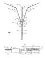
- Figure 1 schematically shows a general view of an embodiment of an apparatus for assembling chip devices between two parallel wires 8a, 8b, for forming a ladder-shaped string of chip devices.
- a series of chip devices 10 awaiting processing are stored in a pile at an input area 12 of the apparatus, for instance a groove adapted to the width of the chip devices.
- Each chip device 10 generally in the shape of a parallelepiped, has two opposite, substantially parallel lateral walls, each provided with a longitudinal groove adapted to the diameter of the wires.
- the chip devices are piled up in area 12 such that their longitudinal grooves are aligned.
- a passive pinching device 14 placed at the bottom of area 12 comprises, in a preferred embodiment, two cylindrical rollers 14a and 14b.
- Passive pinching device it is understood that the rollers 14a, 14b are at a substantially constant distance from each other during operation, i.e. no alternating pinching movement is implemented.
- the axes of the rollers 14a, 14b are substantially perpendicular to the wires, and their spacing is such that two opposing surfaces 16a, 16b of the rollers are at a distance substantially equal to the width of the chip devices (i.e. the distance between the lateral walls of the chip devices).
- the rollers 14a, 14b are a preferred embodiment to define the opposing surfaces 16a, 16b of the pinching device. Indeed, this will reduce friction and wear. They may be comprised of ball bearings. In a less favorable alternative, the opposing surfaces 16a, 16b may be formed by fixed elements.
- Each wire 8a, 8b is fed in continuous motion along a respective opposing surface 16a, 16b, in alignment with the respective grooves of the chip devices in area 12.
- Each wire 8a, 8b is for instance fed from a reel, not shown, over an auxiliary roller 18a, 18b, then along the respective opposing surface 16a, 16b, and leaves the apparatus parallel to the other wire, at the distance defined by the opposing surfaces, thus the chip device size.
- Auxiliary rollers 18a, 18b ensure that the wires 8a, 8b enter the pinching device 14 at an angle avoiding interference with the chip devices 10 stored in area 12.
- the assembled string thus leaving the rollers 14 is for instance stored on a reel, not shown, that may also provide the required traction to pull the wires through the assembly apparatus.
- the chip devices may be fixed to the wires in various manners.
- the wires may be bare metal and the grooves of the chip devices include metal areas.
- the string may then go through a solder bath as it exits the apparatus, whereby the metal areas of the grooves are soldered to the wires.
- the grooves of the chip devices are configured to clip over the wires. No subsequent operation is then required in the assembly.
- one of the rollers 14a, 14b is preferably spring biased towards the other roller.
- the spring force is chosen sufficient to insert the wires in the grooves, but insufficient to break a chip device that has a width larger than the nominal value. This solution moreover allows the processing of chip devices having widths spanning over a range.
- FIG. 1 also partially shows a detail of the chip device feeder 20.
- the feeder comprises three retractable pins 22a-22c, leaving room for a single chip device 10 between two consecutive pins. These pins form part of a device separator, described in more detail below, allowing to take one chip device at a time from the pile of chip devices stored in area 12.
- the separation mechanism preferably operates with the aid of gravity, i.e. the apparatus is tilted so that the pinching device 14 lies below area 12.
- the chip devices in area 12 then pile up naturally against the pins 22a-22c, and will tend to fall naturally as the pins are retracted.
- vibration may be applied to the apparatus.
- the chips may also be transported by aid of an air cushion in combination with either gravity or a pushing mechanism.
- the chips may be transported by mechanical means, e.g. pushing rods.
- the chips may be fed directly to the pinching device 14 by means of a conventional pick-and-place machine used to place surface-mount devices on printed circuit boards.
- FIGS 2A-2F schematically show a side view of the chip device feeder 20, in several steps of processing chip devices.
- the apparatus is shown horizontally, although, as mentioned above, it is rather tilted so that the right portion, comprising the storage area 12, is raised above the left portion.
- roller 14b is shown only on figure 2A ⁇ in figures 2B-2F the rollers are represented by their axes.
- the chip devices 10 slide over plate 24, preferably in a guiding groove. Only the bottom of the guiding groove is visible, the side walls of the groove not being shown for sake of clarity.
- the side walls of the guiding groove are interrupted in the area of rollers 14a and 14b, where the wires enter laterally (wire 8b is shown partially).
- the grooves of the shown chip devices are visible.
- the storage area 12 is partially covered by a plate 26 that prevents the stored chip devices 10 from exiting the groove due to vibrations generated by the apparatus.
- a hook 28 is arranged to alternately take a new chip device from the pile 12 and push it through the rollers 14a, 14b, as explained below.
- pin 22a is retracted and pins 22b and 22b are up.
- a pile of chip devices 10 rests against pin 22b by gravity, covering retracted pin 22a.
- a single chip device 10-1 rests against pin 22c.
- hook 28 arrives from between the rollers, first rising clear of chip device 10-1, then descending behind it, in the gap left between chip device 10-1 and the remaining chip devices retained by pin 22b.
- pin 22b is retracted and pin 22a is raised.
- the chip device 10 that happened to be over pin 22a is lifted against plate 26.
- pin 22a in its raised position, does not protrude more than the clearance between the chip devices and plate 26, thus the chip device 10 over pin 22a can still slide.
- pin 22c is retracted and pin 22b is raised.
- the chip device 10-3 that happened to lie over pin 22b is lifted, but it can still slide.
- pin 22a is retracted and hook 28 starts moving towards the left, accompanying chip device 10-1 over retracted pin 22c towards the rollers.
- Chip 10-3 slides over pin 22b and follows the hook by gravity.
- the chip device 10-4 that was behind chip device 10-3 stops against pin 22b.
- chip device 10-1 is likely to start slipping leftwards by gravity. In the first portion of the travel of chip device 10-1 towards the rollers, hook 28 may have no active role.
- pin 22c is raised as hook 28 travels over it.
- Chip device 10-3 thus stops against pin 22c.
- Hook 28 is shown in its final position where it places chip device 10-1 between the rollers, where the wires are clipped into the chip device's grooves, and the chip device travels further with the wires. In the meantime, further chip devices contained in storage area 12 slide over pin 22a and come to rest against chip device 10-4.
- hook 28 exerts on chip device 10-1 sufficient pressure to start inserting the wires into the chip device's grooves. Gravity alone may not be sufficient for this purpose.
- the cycle then starts over as in figure 2A .
- the pitch of the chip devices in the final string is defined by the wire travel speed and the cycle time of hook 28.
- FIG. 3 shows a general perspective view of a detailed embodiment of the apparatus. Same elements as in the previous figures are designated by same reference numerals.
- Wires 8a and 8b are fed from respective reels 30a and 30b.
- the wires are led to their respective auxiliary rollers through funnel shaped elements 32a, 32b, which ensure that the wires arrive to rollers 18a, 18b at a substantially constant position, regardless of the widely varying exit positions from reels 30a, 30b.
- Hook 28 has a first axis 28-1 by which a back and forth movement is transferred to the hook, and a second axis 28-2 arranged to follow a cam (not shown) that defines the up and down movements of the hook as it travels back and forth.
- plate 24 comprises a split starting near roller 14b and extending along the chip device guiding groove towards the exit area of the apparatus.
- This split defines a splinter-like element 24-1, having a far end, away from roller 14b, integral with plate 24, and a free end, near roller 14b, cut away from the rest of plate 24.
- Roller 14b is mounted on this free end.
- the width and length of element 24-1 define the spring bias force.
- FIG. 3 further shows a hopper 34 containing chip device refills for the storage groove 12.
- Hopper 34 comprises a series of parallel grooves, each containing a pile of chip devices having the desired orientation for assembly on wires 8a and 8b.
- the hopper 34 is initially attached to base plate 24 such that its first groove is in key with the storage groove 12. As soon as the first groove of the hopper is empty, the hopper is shifted by one step, putting its next groove in key with groove 12, and so on until the hopper is empty.
- Each hopper 34 may be pre-filled by a conventional pick-and-place machine used to place surface-mount devices on printed circuit boards.
- Figure 4 shows an enlarged detail of figure 3 , in the area of rollers 14a, 14b, better revealing some shapes that were too small in figure 3 .
- the side walls of the groove in which the chip devices travel are interrupted only in close proximity to the rollers. This ensures that the chip devices are maintained laterally, and don't skew, all along the assembly process.
- the wires are guided in grooves just before they are fed to the rollers. These grooves ensure that the wires arrive on the rollers at the height corresponding to the lateral grooves in the chip devices.
Landscapes
- Engineering & Computer Science (AREA)
- Mechanical Engineering (AREA)
- Supply And Installment Of Electrical Components (AREA)
- Automatic Assembly (AREA)
- Apparatuses And Processes For Manufacturing Resistors (AREA)
- Feeding Of Articles To Conveyors (AREA)
Abstract
Description
- The invention relates to the assembly of small devices, having a size that can be smaller than one millimeter, especially devices embedding a microelectronic chip, on a wire in order to form a string of devices that is better adapted to further processing.
- Patent application
EP2099060 discloses various methods of assembling such chip devices on a wire. Each chip device is provided with a groove adapted to the diameter of the wire. The disclosed methods involve temporarily fixing the chip devices on a tape and using conventional wire-bond equipment to individually run the wire through the groove of each chip device. The wire can be fixed in the grooves by gluing or soldering, or the grooves can be configured so that the wire clips into the grooves. - There is a need for equipment better adapted to assembling chip devices on wires, enabling, in particular, a reduction of manufacturing times.
- This need is addressed by an apparatus for assembling chip devices on a wire, each chip device comprising two substantially parallel lateral walls, and a groove in one of the lateral walls for receiving the wire. The apparatus includes a pinching device comprising two opposing surfaces, the distance between the opposing surfaces being substantially constant and substantially equal to the distance between the two lateral walls of a chip device. A wire feeder is adapted to continuously feed the wire in contact with one of the opposing surfaces of the pinching device. A chip device feeder is adapted to drive chip devices, one at a time, between the opposing surfaces, with their grooves turned towards the wire.
- In a preferred embodiment, the pinching device comprises two cylindrical rollers having rotation axes substantially perpendicular to the wire, said opposing surfaces being formed by respective surfaces of the rollers.
- In a preferred embodiment, the chip device feeder comprises a storage groove adapted to lead a series of chip devices in contact with each other to the pinching device. A separator is arranged near the pinching device for creating a gap between the last and penultimate chip devices in the storage groove. A hook has an alternating movement between a first position in the gap, where it hooks the last chip device, and a second position near said opposing surfaces of the pinching device, where it releases the last chip device.
-
-
Figure 1 schematically shows a general view of an embodiment of an apparatus for assembling chip devices between two parallel wires. -
Figures 2A-2F schematically show a side view of a detail of the apparatus, in several steps of processing chip devices. -
Figure 3 shows a general perspective view of a detailed embodiment of the apparatus. -
Figure 4 shows en enlarged detail offigure 3 . -
Figure 1 schematically shows a general view of an embodiment of an apparatus for assembling chip devices between twoparallel wires - A series of
chip devices 10 awaiting processing are stored in a pile at aninput area 12 of the apparatus, for instance a groove adapted to the width of the chip devices. Eachchip device 10, generally in the shape of a parallelepiped, has two opposite, substantially parallel lateral walls, each provided with a longitudinal groove adapted to the diameter of the wires. The chip devices are piled up inarea 12 such that their longitudinal grooves are aligned. - A passive pinching device 14 placed at the bottom of
area 12 comprises, in a preferred embodiment, twocylindrical rollers rollers rollers opposing surfaces - The
rollers opposing surfaces opposing surfaces - Each
wire opposing surface area 12. Eachwire auxiliary roller opposing surface Auxiliary rollers wires chip devices 10 stored inarea 12. - A
chip device feeder 20 arranged betweenarea 12 and pinching device 14, described in more detail later, takes onechip device 10 at a time fromstorage area 12, and moves it between rollers 14. As the chip device approaches the rollers, its opposite grooves start engaging with thewires opposing surfaces - The assembled string thus leaving the rollers 14 is for instance stored on a reel, not shown, that may also provide the required traction to pull the wires through the assembly apparatus.
- The chip devices may be fixed to the wires in various manners. For example, the wires may be bare metal and the grooves of the chip devices include metal areas. The string may then go through a solder bath as it exits the apparatus, whereby the metal areas of the grooves are soldered to the wires.
- In a preferred embodiment, the grooves of the chip devices are configured to clip over the wires. No subsequent operation is then required in the assembly.
- In order to avoid breaking chip devices that may be wider than a nominal value, one of the
rollers -
Figure 1 also partially shows a detail of thechip device feeder 20. The feeder comprises threeretractable pins 22a-22c, leaving room for asingle chip device 10 between two consecutive pins. These pins form part of a device separator, described in more detail below, allowing to take one chip device at a time from the pile of chip devices stored inarea 12. - The separation mechanism preferably operates with the aid of gravity, i.e. the apparatus is tilted so that the pinching device 14 lies below
area 12. The chip devices inarea 12 then pile up naturally against thepins 22a-22c, and will tend to fall naturally as the pins are retracted. To aid the gravity effect, especially if the chip devices are very small (smaller than one millimeter), vibration may be applied to the apparatus. - Instead of using vibration, the chips may also be transported by aid of an air cushion in combination with either gravity or a pushing mechanism.
- Furthermore, the chips may be transported by mechanical means, e.g. pushing rods.
- Instead of using a
chip device feeder 20 in combination with a separation mechanism, the chips may be fed directly to the pinching device 14 by means of a conventional pick-and-place machine used to place surface-mount devices on printed circuit boards. -
Figures 2A-2F schematically show a side view of thechip device feeder 20, in several steps of processing chip devices. The apparatus is shown horizontally, although, as mentioned above, it is rather tilted so that the right portion, comprising thestorage area 12, is raised above the left portion. - The elements of the apparatus are assembled around a
base plate 24.Roller 14b is shown only onfigure 2A ― infigures 2B-2F the rollers are represented by their axes. Thechip devices 10 slide overplate 24, preferably in a guiding groove. Only the bottom of the guiding groove is visible, the side walls of the groove not being shown for sake of clarity. The side walls of the guiding groove are interrupted in the area ofrollers wire 8b is shown partially). The grooves of the shown chip devices are visible. Thestorage area 12 is partially covered by aplate 26 that prevents the storedchip devices 10 from exiting the groove due to vibrations generated by the apparatus. Ahook 28 is arranged to alternately take a new chip device from thepile 12 and push it through therollers - In
figure 2A ,pin 22a is retracted and pins 22b and 22b are up. A pile ofchip devices 10 rests againstpin 22b by gravity, covering retractedpin 22a. A single chip device 10-1 rests againstpin 22c. As a chip device 10-2 leaves therollers wire 8b inserted in its groove,hook 28 arrives from between the rollers, first rising clear of chip device 10-1, then descending behind it, in the gap left between chip device 10-1 and the remaining chip devices retained bypin 22b. - In
figure 2B ,pin 22b is retracted andpin 22a is raised. Thechip device 10 that happened to be overpin 22a is lifted againstplate 26. However,pin 22a, in its raised position, does not protrude more than the clearance between the chip devices andplate 26, thus thechip device 10 overpin 22a can still slide. - In
figure 2C , the two first chip devices that lied againstpin 22b now slide over retractedpin 22b to come to rest againsthook 28. The remaining chip devices inarea 12 are held back bypin 22a. - In
figure 2D ,pin 22c is retracted andpin 22b is raised. The chip device 10-3 that happened to lie overpin 22b is lifted, but it can still slide. - In
figure 2E ,pin 22a is retracted and hook 28 starts moving towards the left, accompanying chip device 10-1 over retractedpin 22c towards the rollers. Chip 10-3 slides overpin 22b and follows the hook by gravity. The chip device 10-4 that was behind chip device 10-3 stops againstpin 22b. - In fact, as soon as
pin 22c is retracted infigure 2D , chip device 10-1 is likely to start slipping leftwards by gravity. In the first portion of the travel of chip device 10-1 towards the rollers,hook 28 may have no active role. - In
figure 2F ,pin 22c is raised ashook 28 travels over it. Chip device 10-3 thus stops againstpin 22c.Hook 28 is shown in its final position where it places chip device 10-1 between the rollers, where the wires are clipped into the chip device's grooves, and the chip device travels further with the wires. In the meantime, further chip devices contained instorage area 12 slide overpin 22a and come to rest against chip device 10-4. - In this final phase,
hook 28 exerts on chip device 10-1 sufficient pressure to start inserting the wires into the chip device's grooves. Gravity alone may not be sufficient for this purpose. - The cycle then starts over as in
figure 2A . The pitch of the chip devices in the final string is defined by the wire travel speed and the cycle time ofhook 28. -
Figure 3 shows a general perspective view of a detailed embodiment of the apparatus. Same elements as in the previous figures are designated by same reference numerals. -
Wires respective reels elements rollers reels -
Hook 28 has a first axis 28-1 by which a back and forth movement is transferred to the hook, and a second axis 28-2 arranged to follow a cam (not shown) that defines the up and down movements of the hook as it travels back and forth. - In order to ensure a spring bias of
roller 14b towardsroller 14a,plate 24 comprises a split starting nearroller 14b and extending along the chip device guiding groove towards the exit area of the apparatus. This split defines a splinter-like element 24-1, having a far end, away fromroller 14b, integral withplate 24, and a free end, nearroller 14b, cut away from the rest ofplate 24.Roller 14b is mounted on this free end. Thus the width and length of element 24-1 define the spring bias force. -
Figure 3 further shows ahopper 34 containing chip device refills for thestorage groove 12.Hopper 34 comprises a series of parallel grooves, each containing a pile of chip devices having the desired orientation for assembly onwires hopper 34 is initially attached tobase plate 24 such that its first groove is in key with thestorage groove 12. As soon as the first groove of the hopper is empty, the hopper is shifted by one step, putting its next groove in key withgroove 12, and so on until the hopper is empty. - Each
hopper 34 may be pre-filled by a conventional pick-and-place machine used to place surface-mount devices on printed circuit boards. -
Figure 4 shows an enlarged detail offigure 3 , in the area ofrollers figure 3 . As is visible in this figure, the side walls of the groove in which the chip devices travel are interrupted only in close proximity to the rollers. This ensures that the chip devices are maintained laterally, and don't skew, all along the assembly process. - The wires are guided in grooves just before they are fed to the rollers. These grooves ensure that the wires arrive on the rollers at the height corresponding to the lateral grooves in the chip devices.
- Although an assembly of chip devices between two wires has been described as a preferred embodiment, the teachings of the present disclosure apply similarly to the assembly of chip devices on a single wire. In such a case, the apparatus can simply be used with a single wire. One of
rollers rollers
Claims (6)
- Apparatus for assembling chip devices on a wire (8a, 8b), each chip device (10) comprising two substantially parallel lateral walls, and a groove in one of the lateral walls for receiving said wire, characterized in that the apparatus comprises:• a pinching device (14a, 14b) comprising two opposing surfaces (16a, 16b), the distance between the opposing surfaces being substantially constant and substantially equal to the distance between the two lateral walls of a chip device;• a wire feeder adapted to continuously feed said wire in contact with one of the opposing surfaces of the pinching device; and• a chip device feeder (20, 28) adapted to drive chip devices, one at a time, between said opposing surfaces, with their grooves turned towards the wire.
- Apparatus according to claim 1, wherein the pinching device comprises two cylindrical rollers (14a, 14b) having rotation axes substantially perpendicular to the wire, said opposing surfaces (16a, 16b) being formed by respective surfaces of the rollers.
- Apparatus according to claim 2, wherein one of said rollers (14b) is spring biased towards the other roller.
- Apparatus according to claim 1, wherein the chip device feeder comprises:• a storage groove (12) adapted to lead a series of chip devices in contact with each other to the pinching device;• a separator (22a-22c) arranged near the pinching device for creating a gap between the last (10-1) and penultimate chip devices in the storage groove; and• a hook (28) having an alternating movement between a first position in said gap, where it hooks said last chip device (10-1), and a second position near said opposing surfaces of the pinching device, where it releases said last chip device.
- Apparatus according to claim 4, wherein the separator comprises a series of retractable pins (22a-22c) arranged along the feed groove near the pinching device.
- Apparatus according to any of the preceding claims, for assembling chip devices between two wires (8a, 8b), each chip device comprising a groove in each of its lateral walls, the apparatus comprising two wire feeders, each adapted to continuously feed a respective one of the two wires in contact with a respective one of the opposing surfaces (16a, 16b) of the pinching device.
Priority Applications (4)
| Application Number | Priority Date | Filing Date | Title |
|---|---|---|---|
| EP10354024.1A EP2390194B1 (en) | 2010-05-25 | 2010-05-25 | Apparatus for assembling chip devices on wires |
| JP2011116162A JP5788219B2 (en) | 2010-05-25 | 2011-05-24 | Device for assembling chip devices on wires |
| CN201110137407.5A CN102263010B (en) | 2010-05-25 | 2011-05-25 | By chip device assembling equipment on line |
| US13/115,419 US8782880B2 (en) | 2010-05-25 | 2011-05-25 | Apparatus for assembling chip devices on wires |
Applications Claiming Priority (1)
| Application Number | Priority Date | Filing Date | Title |
|---|---|---|---|
| EP10354024.1A EP2390194B1 (en) | 2010-05-25 | 2010-05-25 | Apparatus for assembling chip devices on wires |
Publications (2)
| Publication Number | Publication Date |
|---|---|
| EP2390194A1 true EP2390194A1 (en) | 2011-11-30 |
| EP2390194B1 EP2390194B1 (en) | 2019-12-25 |
Family
ID=42556709
Family Applications (1)
| Application Number | Title | Priority Date | Filing Date |
|---|---|---|---|
| EP10354024.1A Active EP2390194B1 (en) | 2010-05-25 | 2010-05-25 | Apparatus for assembling chip devices on wires |
Country Status (4)
| Country | Link |
|---|---|
| US (1) | US8782880B2 (en) |
| EP (1) | EP2390194B1 (en) |
| JP (1) | JP5788219B2 (en) |
| CN (1) | CN102263010B (en) |
Cited By (2)
| Publication number | Priority date | Publication date | Assignee | Title |
|---|---|---|---|---|
| WO2018138437A1 (en) * | 2017-01-30 | 2018-08-02 | Primo1D | Method for inserting a wire into a groove of a semiconductor chip, and piece of equipment for implementing such a method |
| WO2018193198A1 (en) * | 2017-04-19 | 2018-10-25 | Primo1D | Method for joining a microelectronic chip to a wire element |
Families Citing this family (7)
| Publication number | Priority date | Publication date | Assignee | Title |
|---|---|---|---|---|
| FR3065579B1 (en) | 2017-04-19 | 2019-05-03 | Primo1D | RADIOFREQUENCY RECEIVING TRANSMITTING DEVICE |
| FR3069962B1 (en) | 2017-08-01 | 2020-09-25 | Primo1D | PLATE ANTENNA FOR COUPLING A TRANSMITTER-RECEPTION TERMINAL TO AN RFID DEVICE |
| FR3078980B1 (en) | 2018-03-14 | 2021-06-11 | Primo1D | GUIPED WIRE CONSISTING OF A MAIN CORE AND AT LEAST ONE COVERING WIRE AND INCLUDING AT LEAST ONE CONDUCTIVE WIRED ELEMENT ELECTRICALLY CONNECTED TO AT LEAST ONE ELECTRONIC CHIP |
| FR3103043B1 (en) | 2019-11-08 | 2022-08-05 | Primo1D | ELECTRONIC IDENTIFICATION TAG COMPRISING A WIRED ELECTRONIC IDENTIFICATION DEVICE, METHOD FOR MANUFACTURING SUCH A LABEL AND TEXTILE PART PROVIDED WITH SUCH A LABEL. |
| FR3103630B1 (en) | 2019-11-22 | 2022-06-03 | Primo1D | FUNCTIONAL CHIP ADAPTED TO BE ASSEMBLED WITH WIRED ELEMENTS, AND METHOD FOR MANUFACTURING SUCH A CHIP |
| EP3923195B1 (en) | 2020-06-11 | 2023-08-23 | Primo1D | Electronic label with a flexible and deformable nature |
| FR3150613B1 (en) | 2023-06-30 | 2025-12-12 | Primo1D | Radio frequency transmission and reception device comprising a conductive wire forming an antenna wound in turns |
Citations (5)
| Publication number | Priority date | Publication date | Assignee | Title |
|---|---|---|---|---|
| GB2017038A (en) * | 1978-03-25 | 1979-10-03 | Weresch T | Apparatus for stringing electrical components having two aligned connecting wires into a belt |
| WO1996023432A2 (en) * | 1995-01-25 | 1996-08-08 | Trion Industries, Inc. | Rack and shelving system, and method and apparatus for manufacture thereof |
| US20050116387A1 (en) * | 2003-12-01 | 2005-06-02 | Davison Peter A. | Component packaging apparatus, systems, and methods |
| JP2008124231A (en) * | 2006-11-13 | 2008-05-29 | Taiyo Yuden Co Ltd | Electronic component-link and its manufacturing method |
| EP2099060A1 (en) | 2008-03-06 | 2009-09-09 | Commissariat à l'Energie Atomique | Method and device for manufacturing an assembly with at least two microelectronic chips |
Family Cites Families (3)
| Publication number | Priority date | Publication date | Assignee | Title |
|---|---|---|---|---|
| JPS5254165A (en) * | 1975-10-29 | 1977-05-02 | Murata Manufacturing Co | Apparatus for continuously fixing plurality of electronic parts on tapelike holder |
| US4016935A (en) * | 1975-11-11 | 1977-04-12 | Miller Maurice E | Harrow disc gang |
| US4753061A (en) * | 1986-06-20 | 1988-06-28 | Electro Scientific Industries, Inc. | Method of and apparatus for packaging chip components |
-
2010
- 2010-05-25 EP EP10354024.1A patent/EP2390194B1/en active Active
-
2011
- 2011-05-24 JP JP2011116162A patent/JP5788219B2/en not_active Expired - Fee Related
- 2011-05-25 US US13/115,419 patent/US8782880B2/en active Active
- 2011-05-25 CN CN201110137407.5A patent/CN102263010B/en not_active Expired - Fee Related
Patent Citations (5)
| Publication number | Priority date | Publication date | Assignee | Title |
|---|---|---|---|---|
| GB2017038A (en) * | 1978-03-25 | 1979-10-03 | Weresch T | Apparatus for stringing electrical components having two aligned connecting wires into a belt |
| WO1996023432A2 (en) * | 1995-01-25 | 1996-08-08 | Trion Industries, Inc. | Rack and shelving system, and method and apparatus for manufacture thereof |
| US20050116387A1 (en) * | 2003-12-01 | 2005-06-02 | Davison Peter A. | Component packaging apparatus, systems, and methods |
| JP2008124231A (en) * | 2006-11-13 | 2008-05-29 | Taiyo Yuden Co Ltd | Electronic component-link and its manufacturing method |
| EP2099060A1 (en) | 2008-03-06 | 2009-09-09 | Commissariat à l'Energie Atomique | Method and device for manufacturing an assembly with at least two microelectronic chips |
Non-Patent Citations (1)
| Title |
|---|
| JEAN BRUN ET AL: "Packaging and wired interconnections for insertion of miniaturized chips in smart fabrics", MICROELECTRONICS AND PACKAGING CONFERENCE, 2009. EMPC 2009. EUROPEAN, IEEE, PISCATAWAY, NJ, USA, 15 June 2009 (2009-06-15), pages 1 - 5, XP031534243, ISBN: 978-1-4244-4722-0 * |
Cited By (6)
| Publication number | Priority date | Publication date | Assignee | Title |
|---|---|---|---|---|
| WO2018138437A1 (en) * | 2017-01-30 | 2018-08-02 | Primo1D | Method for inserting a wire into a groove of a semiconductor chip, and piece of equipment for implementing such a method |
| FR3062515A1 (en) * | 2017-01-30 | 2018-08-03 | Primo1D | METHOD OF INSERTING A WIRE INTO A GROOVE OF A SEMICONDUCTOR CHIP, AND EQUIPMENT FOR IMPLEMENTING SUCH A METHOD |
| WO2018193198A1 (en) * | 2017-04-19 | 2018-10-25 | Primo1D | Method for joining a microelectronic chip to a wire element |
| FR3065578A1 (en) * | 2017-04-19 | 2018-10-26 | Primo1D | METHOD FOR ASSEMBLING A MICROELECTRONIC CHIP ON A WIRED ELEMENT |
| US11081466B2 (en) | 2017-04-19 | 2021-08-03 | Primo1D | Method for joining a micorelectronic chip to a wire element |
| EP3613074B1 (en) * | 2017-04-19 | 2022-06-22 | Primo1D | Method for joining a microelectronic chip to a wire element |
Also Published As
| Publication number | Publication date |
|---|---|
| US8782880B2 (en) | 2014-07-22 |
| US20120073128A1 (en) | 2012-03-29 |
| CN102263010B (en) | 2016-03-02 |
| CN102263010A (en) | 2011-11-30 |
| JP2011249808A (en) | 2011-12-08 |
| JP5788219B2 (en) | 2015-09-30 |
| EP2390194B1 (en) | 2019-12-25 |
Similar Documents
| Publication | Publication Date | Title |
|---|---|---|
| EP2390194B1 (en) | Apparatus for assembling chip devices on wires | |
| CN104426309B (en) | Coil segment manufacturing apparatus and coil segment manufacturing method | |
| CN102378571B (en) | The equipment of installation elements and method | |
| EP3250019A1 (en) | Feeder device | |
| US6971415B2 (en) | Rotational grip twist machine and method for fabricating bulges of twisted wire electrical connectors | |
| JP6280817B2 (en) | Component mounting device | |
| US6530511B2 (en) | Wire feed mechanism and method used for fabricating electrical connectors | |
| JP4924459B2 (en) | Tape feeder | |
| WO2013111369A1 (en) | Electrical wire holding bar conveying device | |
| EP3386286B1 (en) | Power supply control device and power supply control method for component supply device | |
| KR101690581B1 (en) | Part supply unit | |
| CN111034384B (en) | Component mounting machine | |
| JP2014200854A (en) | Heat exchanger core temporary mounting device | |
| JP5623441B2 (en) | Parts supply device | |
| JP2022155365A (en) | Stator core manufacturing equipment | |
| KR101115949B1 (en) | Lead Frame Feeder for LED Module | |
| JPH1154989A (en) | Electronic component supply device | |
| CN109775011B (en) | Braiding device and braiding method | |
| KR20260045317A (en) | Coil feeding apparatus for motor hairpin manufacturing | |
| CN119059371A (en) | Bobbin handling device | |
| EP3429327A1 (en) | Part extracting method | |
| JP2015145040A (en) | Bar supply machine | |
| JP2014213367A (en) | Heat exchanger core temporary assembling device | |
| JP6582784B2 (en) | Component positioning device, component insertion device | |
| JP2001122214A (en) | Embossed taping machine with multi-cavity unit |
Legal Events
| Date | Code | Title | Description |
|---|---|---|---|
| AK | Designated contracting states |
Kind code of ref document: A1 Designated state(s): AL AT BE BG CH CY CZ DE DK EE ES FI FR GB GR HR HU IE IS IT LI LT LU LV MC MK MT NL NO PL PT RO SE SI SK SM TR |
|
| AX | Request for extension of the european patent |
Extension state: BA ME RS |
|
| PUAI | Public reference made under article 153(3) epc to a published international application that has entered the european phase |
Free format text: ORIGINAL CODE: 0009012 |
|
| 17P | Request for examination filed |
Effective date: 20120524 |
|
| STAA | Information on the status of an ep patent application or granted ep patent |
Free format text: STATUS: EXAMINATION IS IN PROGRESS |
|
| 17Q | First examination report despatched |
Effective date: 20181026 |
|
| REG | Reference to a national code |
Ref country code: DE Ref legal event code: R079 Ref document number: 602010062495 Country of ref document: DE Free format text: PREVIOUS MAIN CLASS: B65B0059000000 Ipc: B65B0015000000 |
|
| GRAP | Despatch of communication of intention to grant a patent |
Free format text: ORIGINAL CODE: EPIDOSNIGR1 |
|
| STAA | Information on the status of an ep patent application or granted ep patent |
Free format text: STATUS: GRANT OF PATENT IS INTENDED |
|
| RIC1 | Information provided on ipc code assigned before grant |
Ipc: B65B 15/00 20060101AFI20190703BHEP Ipc: H01L 25/065 20060101ALI20190703BHEP |
|
| INTG | Intention to grant announced |
Effective date: 20190722 |
|
| GRAS | Grant fee paid |
Free format text: ORIGINAL CODE: EPIDOSNIGR3 |
|
| GRAA | (expected) grant |
Free format text: ORIGINAL CODE: 0009210 |
|
| STAA | Information on the status of an ep patent application or granted ep patent |
Free format text: STATUS: THE PATENT HAS BEEN GRANTED |
|
| AK | Designated contracting states |
Kind code of ref document: B1 Designated state(s): AL AT BE BG CH CY CZ DE DK EE ES FI FR GB GR HR HU IE IS IT LI LT LU LV MC MK MT NL NO PL PT RO SE SI SK SM TR |
|
| REG | Reference to a national code |
Ref country code: GB Ref legal event code: FG4D |
|
| REG | Reference to a national code |
Ref country code: CH Ref legal event code: EP |
|
| REG | Reference to a national code |
Ref country code: DE Ref legal event code: R096 Ref document number: 602010062495 Country of ref document: DE |
|
| REG | Reference to a national code |
Ref country code: AT Ref legal event code: REF Ref document number: 1216856 Country of ref document: AT Kind code of ref document: T Effective date: 20200115 |
|
| REG | Reference to a national code |
Ref country code: IE Ref legal event code: FG4D |
|
| REG | Reference to a national code |
Ref country code: NL Ref legal event code: MP Effective date: 20191225 |
|
| PG25 | Lapsed in a contracting state [announced via postgrant information from national office to epo] |
Ref country code: LT Free format text: LAPSE BECAUSE OF FAILURE TO SUBMIT A TRANSLATION OF THE DESCRIPTION OR TO PAY THE FEE WITHIN THE PRESCRIBED TIME-LIMIT Effective date: 20191225 Ref country code: NO Free format text: LAPSE BECAUSE OF FAILURE TO SUBMIT A TRANSLATION OF THE DESCRIPTION OR TO PAY THE FEE WITHIN THE PRESCRIBED TIME-LIMIT Effective date: 20200325 Ref country code: GR Free format text: LAPSE BECAUSE OF FAILURE TO SUBMIT A TRANSLATION OF THE DESCRIPTION OR TO PAY THE FEE WITHIN THE PRESCRIBED TIME-LIMIT Effective date: 20200326 Ref country code: LV Free format text: LAPSE BECAUSE OF FAILURE TO SUBMIT A TRANSLATION OF THE DESCRIPTION OR TO PAY THE FEE WITHIN THE PRESCRIBED TIME-LIMIT Effective date: 20191225 Ref country code: SE Free format text: LAPSE BECAUSE OF FAILURE TO SUBMIT A TRANSLATION OF THE DESCRIPTION OR TO PAY THE FEE WITHIN THE PRESCRIBED TIME-LIMIT Effective date: 20191225 Ref country code: BG Free format text: LAPSE BECAUSE OF FAILURE TO SUBMIT A TRANSLATION OF THE DESCRIPTION OR TO PAY THE FEE WITHIN THE PRESCRIBED TIME-LIMIT Effective date: 20200325 Ref country code: FI Free format text: LAPSE BECAUSE OF FAILURE TO SUBMIT A TRANSLATION OF THE DESCRIPTION OR TO PAY THE FEE WITHIN THE PRESCRIBED TIME-LIMIT Effective date: 20191225 |
|
| REG | Reference to a national code |
Ref country code: LT Ref legal event code: MG4D |
|
| PG25 | Lapsed in a contracting state [announced via postgrant information from national office to epo] |
Ref country code: HR Free format text: LAPSE BECAUSE OF FAILURE TO SUBMIT A TRANSLATION OF THE DESCRIPTION OR TO PAY THE FEE WITHIN THE PRESCRIBED TIME-LIMIT Effective date: 20191225 |
|
| PG25 | Lapsed in a contracting state [announced via postgrant information from national office to epo] |
Ref country code: AL Free format text: LAPSE BECAUSE OF FAILURE TO SUBMIT A TRANSLATION OF THE DESCRIPTION OR TO PAY THE FEE WITHIN THE PRESCRIBED TIME-LIMIT Effective date: 20191225 |
|
| PG25 | Lapsed in a contracting state [announced via postgrant information from national office to epo] |
Ref country code: EE Free format text: LAPSE BECAUSE OF FAILURE TO SUBMIT A TRANSLATION OF THE DESCRIPTION OR TO PAY THE FEE WITHIN THE PRESCRIBED TIME-LIMIT Effective date: 20191225 Ref country code: PT Free format text: LAPSE BECAUSE OF FAILURE TO SUBMIT A TRANSLATION OF THE DESCRIPTION OR TO PAY THE FEE WITHIN THE PRESCRIBED TIME-LIMIT Effective date: 20200520 Ref country code: RO Free format text: LAPSE BECAUSE OF FAILURE TO SUBMIT A TRANSLATION OF THE DESCRIPTION OR TO PAY THE FEE WITHIN THE PRESCRIBED TIME-LIMIT Effective date: 20191225 Ref country code: CZ Free format text: LAPSE BECAUSE OF FAILURE TO SUBMIT A TRANSLATION OF THE DESCRIPTION OR TO PAY THE FEE WITHIN THE PRESCRIBED TIME-LIMIT Effective date: 20191225 Ref country code: NL Free format text: LAPSE BECAUSE OF FAILURE TO SUBMIT A TRANSLATION OF THE DESCRIPTION OR TO PAY THE FEE WITHIN THE PRESCRIBED TIME-LIMIT Effective date: 20191225 |
|
| PG25 | Lapsed in a contracting state [announced via postgrant information from national office to epo] |
Ref country code: SM Free format text: LAPSE BECAUSE OF FAILURE TO SUBMIT A TRANSLATION OF THE DESCRIPTION OR TO PAY THE FEE WITHIN THE PRESCRIBED TIME-LIMIT Effective date: 20191225 Ref country code: SK Free format text: LAPSE BECAUSE OF FAILURE TO SUBMIT A TRANSLATION OF THE DESCRIPTION OR TO PAY THE FEE WITHIN THE PRESCRIBED TIME-LIMIT Effective date: 20191225 Ref country code: IS Free format text: LAPSE BECAUSE OF FAILURE TO SUBMIT A TRANSLATION OF THE DESCRIPTION OR TO PAY THE FEE WITHIN THE PRESCRIBED TIME-LIMIT Effective date: 20200425 |
|
| REG | Reference to a national code |
Ref country code: DE Ref legal event code: R097 Ref document number: 602010062495 Country of ref document: DE |
|
| PG25 | Lapsed in a contracting state [announced via postgrant information from national office to epo] |
Ref country code: ES Free format text: LAPSE BECAUSE OF FAILURE TO SUBMIT A TRANSLATION OF THE DESCRIPTION OR TO PAY THE FEE WITHIN THE PRESCRIBED TIME-LIMIT Effective date: 20191225 Ref country code: DK Free format text: LAPSE BECAUSE OF FAILURE TO SUBMIT A TRANSLATION OF THE DESCRIPTION OR TO PAY THE FEE WITHIN THE PRESCRIBED TIME-LIMIT Effective date: 20191225 |
|
| PLBE | No opposition filed within time limit |
Free format text: ORIGINAL CODE: 0009261 |
|
| STAA | Information on the status of an ep patent application or granted ep patent |
Free format text: STATUS: NO OPPOSITION FILED WITHIN TIME LIMIT |
|
| REG | Reference to a national code |
Ref country code: AT Ref legal event code: MK05 Ref document number: 1216856 Country of ref document: AT Kind code of ref document: T Effective date: 20191225 |
|
| PG25 | Lapsed in a contracting state [announced via postgrant information from national office to epo] |
Ref country code: SI Free format text: LAPSE BECAUSE OF FAILURE TO SUBMIT A TRANSLATION OF THE DESCRIPTION OR TO PAY THE FEE WITHIN THE PRESCRIBED TIME-LIMIT Effective date: 20191225 |
|
| 26N | No opposition filed |
Effective date: 20200928 |
|
| PG25 | Lapsed in a contracting state [announced via postgrant information from national office to epo] |
Ref country code: LI Free format text: LAPSE BECAUSE OF NON-PAYMENT OF DUE FEES Effective date: 20200531 Ref country code: MC Free format text: LAPSE BECAUSE OF FAILURE TO SUBMIT A TRANSLATION OF THE DESCRIPTION OR TO PAY THE FEE WITHIN THE PRESCRIBED TIME-LIMIT Effective date: 20191225 Ref country code: CH Free format text: LAPSE BECAUSE OF NON-PAYMENT OF DUE FEES Effective date: 20200531 Ref country code: IT Free format text: LAPSE BECAUSE OF FAILURE TO SUBMIT A TRANSLATION OF THE DESCRIPTION OR TO PAY THE FEE WITHIN THE PRESCRIBED TIME-LIMIT Effective date: 20191225 Ref country code: AT Free format text: LAPSE BECAUSE OF FAILURE TO SUBMIT A TRANSLATION OF THE DESCRIPTION OR TO PAY THE FEE WITHIN THE PRESCRIBED TIME-LIMIT Effective date: 20191225 |
|
| PG25 | Lapsed in a contracting state [announced via postgrant information from national office to epo] |
Ref country code: PL Free format text: LAPSE BECAUSE OF FAILURE TO SUBMIT A TRANSLATION OF THE DESCRIPTION OR TO PAY THE FEE WITHIN THE PRESCRIBED TIME-LIMIT Effective date: 20191225 |
|
| REG | Reference to a national code |
Ref country code: BE Ref legal event code: MM Effective date: 20200531 |
|
| PG25 | Lapsed in a contracting state [announced via postgrant information from national office to epo] |
Ref country code: LU Free format text: LAPSE BECAUSE OF NON-PAYMENT OF DUE FEES Effective date: 20200525 |
|
| PG25 | Lapsed in a contracting state [announced via postgrant information from national office to epo] |
Ref country code: IE Free format text: LAPSE BECAUSE OF NON-PAYMENT OF DUE FEES Effective date: 20200525 |
|
| PG25 | Lapsed in a contracting state [announced via postgrant information from national office to epo] |
Ref country code: BE Free format text: LAPSE BECAUSE OF NON-PAYMENT OF DUE FEES Effective date: 20200531 |
|
| PG25 | Lapsed in a contracting state [announced via postgrant information from national office to epo] |
Ref country code: TR Free format text: LAPSE BECAUSE OF FAILURE TO SUBMIT A TRANSLATION OF THE DESCRIPTION OR TO PAY THE FEE WITHIN THE PRESCRIBED TIME-LIMIT Effective date: 20191225 Ref country code: MT Free format text: LAPSE BECAUSE OF FAILURE TO SUBMIT A TRANSLATION OF THE DESCRIPTION OR TO PAY THE FEE WITHIN THE PRESCRIBED TIME-LIMIT Effective date: 20191225 Ref country code: CY Free format text: LAPSE BECAUSE OF FAILURE TO SUBMIT A TRANSLATION OF THE DESCRIPTION OR TO PAY THE FEE WITHIN THE PRESCRIBED TIME-LIMIT Effective date: 20191225 |
|
| PG25 | Lapsed in a contracting state [announced via postgrant information from national office to epo] |
Ref country code: MK Free format text: LAPSE BECAUSE OF FAILURE TO SUBMIT A TRANSLATION OF THE DESCRIPTION OR TO PAY THE FEE WITHIN THE PRESCRIBED TIME-LIMIT Effective date: 20191225 |
|
| PGFP | Annual fee paid to national office [announced via postgrant information from national office to epo] |
Ref country code: GB Payment date: 20220523 Year of fee payment: 13 Ref country code: FR Payment date: 20220525 Year of fee payment: 13 Ref country code: DE Payment date: 20220519 Year of fee payment: 13 |
|
| REG | Reference to a national code |
Ref country code: DE Ref legal event code: R119 Ref document number: 602010062495 Country of ref document: DE |
|
| GBPC | Gb: european patent ceased through non-payment of renewal fee |
Effective date: 20230525 |
|
| PG25 | Lapsed in a contracting state [announced via postgrant information from national office to epo] |
Ref country code: DE Free format text: LAPSE BECAUSE OF NON-PAYMENT OF DUE FEES Effective date: 20231201 Ref country code: GB Free format text: LAPSE BECAUSE OF NON-PAYMENT OF DUE FEES Effective date: 20230525 |
|
| PG25 | Lapsed in a contracting state [announced via postgrant information from national office to epo] |
Ref country code: FR Free format text: LAPSE BECAUSE OF NON-PAYMENT OF DUE FEES Effective date: 20230531 |