EP2387255A2 - Acoustic sensor and microphone - Google Patents
Acoustic sensor and microphone Download PDFInfo
- Publication number
- EP2387255A2 EP2387255A2 EP11165749A EP11165749A EP2387255A2 EP 2387255 A2 EP2387255 A2 EP 2387255A2 EP 11165749 A EP11165749 A EP 11165749A EP 11165749 A EP11165749 A EP 11165749A EP 2387255 A2 EP2387255 A2 EP 2387255A2
- Authority
- EP
- European Patent Office
- Prior art keywords
- acoustic
- extraction wiring
- region
- vicinity
- perforation
- Prior art date
- Legal status (The legal status is an assumption and is not a legal conclusion. Google has not performed a legal analysis and makes no representation as to the accuracy of the status listed.)
- Granted
Links
Images




Classifications
-
- H—ELECTRICITY
- H04—ELECTRIC COMMUNICATION TECHNIQUE
- H04R—LOUDSPEAKERS, MICROPHONES, GRAMOPHONE PICK-UPS OR LIKE ACOUSTIC ELECTROMECHANICAL TRANSDUCERS; ELECTRIC HEARING AIDS; PUBLIC ADDRESS SYSTEMS
- H04R19/00—Electrostatic transducers
- H04R19/04—Microphones
-
- H—ELECTRICITY
- H04—ELECTRIC COMMUNICATION TECHNIQUE
- H04R—LOUDSPEAKERS, MICROPHONES, GRAMOPHONE PICK-UPS OR LIKE ACOUSTIC ELECTROMECHANICAL TRANSDUCERS; ELECTRIC HEARING AIDS; PUBLIC ADDRESS SYSTEMS
- H04R19/00—Electrostatic transducers
- H04R19/005—Electrostatic transducers using semiconductor materials
-
- B—PERFORMING OPERATIONS; TRANSPORTING
- B81—MICROSTRUCTURAL TECHNOLOGY
- B81B—MICROSTRUCTURAL DEVICES OR SYSTEMS, e.g. MICROMECHANICAL DEVICES
- B81B3/00—Devices comprising flexible or deformable elements, e.g. comprising elastic tongues or membranes
-
- H—ELECTRICITY
- H04—ELECTRIC COMMUNICATION TECHNIQUE
- H04R—LOUDSPEAKERS, MICROPHONES, GRAMOPHONE PICK-UPS OR LIKE ACOUSTIC ELECTROMECHANICAL TRANSDUCERS; ELECTRIC HEARING AIDS; PUBLIC ADDRESS SYSTEMS
- H04R1/00—Details of transducers, loudspeakers or microphones
- H04R1/06—Arranging circuit leads; Relieving strain on circuit leads
Definitions
- the present invention relates to acoustic sensors and microphones, and specifically to an MEMS (Micro Electro Mechanical Systems) type acoustic sensor manufactured by using the MEMS technique, and a microphone using such acoustic sensor.
- MEMS Micro Electro Mechanical Systems
- a capacitance type acoustic sensor is dislosed in Japanese Patent Publication No. 4338395 and Japanese Unexamined Patent Publication No. 2009-89097 .
- a diaphragm movable electrode film
- a back plate is fixed on the front surface of the silicon substrate so as to cover the diaphragm
- a capacitor is configured by the fixed electrode film and the diaphragm of the back plate.
- the diaphragm is vibrated with the acoustic vibration, and the change in electrostatic capacitance between the fixed electrode firm and the diaphragm in such case is output.
- a great number of acoustic holes is opened in the back plate since the acoustic vibration needs to be introduced to an air gap between the fixed electrode film and the diaphragm in order to vibrate the diaphragm with the acoustic vibration.
- the opening size of the acoustic hole needs to be made large to enhance the S/N ratio.
- the acoustic hole that is opened in the back plate is opened not only at the plate portion having a relatively thick film thickness but also at the fixed electrode film having a thin thickness. Therefore, if the opening size of the acoustic hole is made large, the extraction wiring portion of the fixed electrode film may easily break or the parasitic resistance may increase.
- the present invention has been devised to solve the problems described above, and an object thereof is to provide an acoustic sensor in which the fixed electrode film is less likely to break and the parasitic resistance is less likely to increase even if the opening size of the acoustic hole (acoustic perforation) opened in the back plate is made large.
- an acoustic sensor including: a semiconductor substrate including a back chamber; a conductive diaphragm arranged on an upper side of the semiconductor substrate; an insulating fixed film fixed on an upper surface of the semiconductor substrate to cover the diaphragm with a gap; a conductive fixed electrode film arranged on the fixed film at a position facing the diaphragm; an extraction wiring extracted from the fixed electrode film; and an electrode pad, to which the extraction wiring is connected; the acoustic sensor converting an acoustic vibration to change in electrostatic capacitance between the diaphragm and the fixed electrode film; wherein a plurality of acoustic perforations is opened in a back plate including the fixed film and the fixed electrode film; and an opening rate of the acoustic perforation is smaller in the extraction wiring and a region in the vicinity thereof than in other regions.
- the opening rate is the ratio of the total of the opening area of the acoustic perforations with respect to the area of the region in the relevant region of an extent including a plurality of acoustic perforations.
- the opening area per one acoustic perforation is to be reduced compared to other regions in the extraction wiring and the region in the vicinity of the extraction wiring.
- the inter-center distance between the adjacent acoustic perforations is made longer than other regions in the extraction wiring and the region in the vicinity of the extraction wiring.
- the extraction wiring and the region in the vicinity of the extraction wiring includes an acoustic perforation having a smaller opening rate than the acoustic perforation in other regions, this includes a case where the extraction wiring or the region in the vicinity of the extraction wiring does not include the acoustic perforations (i.e., opening rate is zero).
- the region in the vicinity of the extraction wiring refers to the region within six times and preferably the region within substantially three times the average inter-center distance of the acoustic perforation measured from the basal end of the extraction wiring of the acoustic perforation formed region (excluding the region where the extraction wiring passes) of the back plate.
- the acoustic perforation in the extraction wiring and in the region in the vicinity thereof has a relatively small opening rate, and hence the width of the electrode film between the acoustic perforations in the extraction wiring and in the region in the vicinity thereof is less likely to become narrow and the parasitic resistance in the extraction wiring and in the region in the vicinity thereof can be reduced. Therefore, the generation of noise in the extraction wiring and in the region in the vicinity thereof can be reduced and the S/N ratio of the acoustic sensor can be enhanced.
- the width of the electrode film between the acoustic perforations can be widened in the extraction wiring and in the region in the vicinity thereof, so that the lowering of the strength of the fixed electrode film by the acoustic perforation in the extraction wiring and in the region in the vicinity thereof can be reduced. Therefore, the mechanical strength of the extraction wiring and the fixed electrode film increase, so that disconnection and breakage are less likely to occur.
- the opening rate of the acoustic perforation is relatively large in other regions excluding the extraction wiring and the vicinity thereof so that the acoustic vibration easily passes through the acoustic perforation, and the S/N ratio of the acoustic sensor is increased to enhance the sensitivity.
- One embodiment of the first acoustic sensor according to the present invention has the acoustic perforation arranged in the extraction wiring and the region in the vicinity of the extraction wiring, and the acoustic perforation in other regions excluding the extraction wiring and the region in the vicinity thereof arrayed according to the same rule.
- the sacrifice layer of the air gap can be uniformly etched in the manufacturing step.
- a diameter of the acoustic perforation having a relatively small opening area arranged in the extraction wiring or the region in the vicinity of the extraction wiring is smaller than twice a spaced distance between the acoustic perforations. According to such embodiment, the strength of the fixed electrode film can be ensured and the parasitic resistance can be reduced.
- a diameter of the acoustic perforation having a relatively large opening area arranged in other regions excluding the extraction wiring and the region in the vicinity of the extraction wiring is greater than a spaced distance between the acoustic perforations. According to such embodiment, the S/N ratio of the acoustic sensor can be enhanced since the opening rate of the acoustic perforation becomes large in other regions excluding the extraction wiring and the region in the vicinity of the extraction wiring.
- a diameter of the acoustic perforation having a relatively large opening area arranged in other regions excluding the extraction wiring and the region in the vicinity of the extraction wiring is smaller than four times a spaced distance between the acoustic perforations. According to such embodiment, the strength of the back plate can be prevented from lacking by making the opening area of the acoustic perforation too large, and the electrode area of the fixed electrode film can be prevented from becoming too small.
- an inter-center distance between the adjacent acoustic perforations of the acoustic perforations having a relatively small opening area arrayed in the extraction wiring and the region in the vicinity of the extracting wiring is equal to an inter-center distance between the adjacent acoustic perforations of the acoustic perforations having a relatively large opening area arranged in other regions excluding the extraction wiring and the region in the vicinity of the extraction wiring.
- the sacrifice layer of the air gap can be uniformly etched in the manufacturing step.
- the acoustic perforation contained in five or less zones including the acoustic perforation of the extraction wiring when counting from the acoustic perforation arranged at the extraction wiring is the acoustic perforation having a relatively small opening area.
- zones this refers to the virtual line passing through the centers of a plurality of acoustic perforations at substantially equal distance from the extraction wiring. According to such embodiment, the strength of the back plate can be ensured and the parasitic resistance can be reduced.
- an acoustic sensor including: a semiconductor substrate including a back chamber; a conductive diaphragm arranged on an upper side of the semiconductor substrate; an insulating fixed film fixed on an upper surface of the semiconductor substrate to cover the diaphragm with a gap; a conductive fixed electrode film arranged on the fixed film at a position facing the diaphragm; an extraction wiring extracted from the fixed electrode film; and an electrode pad, to which the extraction wiring is connected; the acoustic sensor converting an acoustic vibration to change in electrostatic capacitance between the diaphragm and the fixed electrode film; wherein a plurality of acoustic perforations is opened in a back plate including the fixed film and the fixed electrode film; and at least the extraction wiring, of the extraction wiring and a region in the vicinity of thereof, does not include the acoustic perforation or includes an acoustic perforation of small opening rate compared to an acoustic
- the opening rate is the ratio of the total of the opening area of the acoustic perforations with respect to the area of the region in the relevant region of an extent including a plurality of acoustic perforations.
- the opening area per one acoustic perforation is to be reduced compared to the acoustic perforation in other regions excluding the extraction wiring and the region in the vicinity of the extraction wiring.
- the inter-center distance between the adjacent acoustic perforations is made longer than the acoustic perforation in other regions excluding the extraction wiring and the region in the vicinity of the extraction wiring.
- the region in the vicinity of the extraction wiring refers to the region within six times and preferably the region within substantially three times the average inter-center distance of the acoustic perforation measured from the basal end of the extraction wiring of the acoustic perforation formed region (excluding the region where the extraction wiring passes) of the back plate.
- the acoustic perforation in the extraction wiring and in the region in the vicinity thereof has a relatively small opening rate, or does the acoustic perforation is not provided, and hence the width of the electrode film between the acoustic perforations in the extraction wiring and in the region in the vicinity thereof is less likely to become narrow and the parasitic resistance in the extraction wiring and in the region in the vicinity thereof can be reduced. Therefore, the generation of noise in the extraction wiring and in the region in the vicinity thereof can be reduced and the S/N ratio of the acoustic sensor can be enhanced.
- the width of the electrode film between the acoustic perforations can be widened in the extraction wiring and in the region in the vicinity thereof, so that the lowering of the strength of the fixed electrode film by the acoustic perforation in the extraction wiring and in the region in the vicinity thereof can be reduced. Therefore, the mechanical strength of the extraction wiring and the fixed electrode film increase, so that disconnection and breakage are less likely to occur.
- the opening rate of the acoustic perforation is relatively large in other regions excluding the extraction wiring and the vicinity thereof so that the acoustic vibration easily passes through the acoustic perforation, and the S/N ratio of the acoustic sensor is increased to enhance the sensitivity.
- a first microphone according to the present invention has a first acoustic sensor according to the present invention and a signal processing circuit for processing an electrical signal output from the acoustic sensor accommodated in a housing.
- the generation of noise can be reduced and the S/N ratio of the microphone can be enhanced since the acoustic sensor of the present invention is used.
- the disconnection and breakage of the extraction wiring and the fixed electrode film in the acoustic sensor are less likely to occur, and the failure of the microphone is less likely to occur.
- a second microphone according to the present invention has a second acoustic sensor according to the present invention and a signal processing circuit for processing an electrical signal output from the acoustic sensor accommodated in a housing.
- the generation of noise can be reduced and the S/N ratio of the microphone can be enhanced since the acoustic sensor of the present invention is used.
- the disconnection and breakage of the extraction wiring and the fixed electrode film in the acoustic sensor are less likely to occur, and the failure of the microphone is less likely to occur.
- the means for solving the problems of the invention has a characteristic of appropriately combining the configuring elements described above, and the present invention enables a great number of variations by the combination of the configuring elements.
- Fig. 1 is a plan view of the acoustic sensor 31.
- Fig. 2 is a cross-sectional view in a diagonal direction of the acoustic sensor 31 (cross-section taken along line X-X of Fig. 1 ).
- the acoustic sensor 31 is a capacitance type element manufactured by using the MEMS technique. As shown in Fig. 2 , a diaphragm 33 is arranged on an upper surface of a silicon substrate 32 (semiconductor substrate) by way of an anchor 37, and a back plate 34 is fixed thereon by way of a microscopic air gap.
- the silicon substrate 32 made of monocrystalline silicon is formed with a back chamber 35 passed through from the front surface to the back surface.
- the inner peripheral surface of the back chamber 35 may be a perpendicular surface or may be inclined to a tapered shape.
- a plurality of anchors 37 for supporting the lower surface of the outer peripheral part of the diaphragm 33 is arranged on the upper surface of the silicon substrate 32, and a base part 41 of thick film is formed on the upper surface of the silicon substrate 32 to surround the diaphragm 33. Furthermore, the region on the outer side than the base part 41 in the upper surface of the silicon substrate 32 is covered with an adhering layer 47 thinner than the base part 41.
- the anchor 37 and the base part 41 are formed by SiO 2 .
- the adhering layer 47 is made by SiO 2 or polysilicon.
- the diaphragm 33 is formed by a substantially circular plate shaped polysilicon thin firm, and has conductivity.
- a band plate shaped extraction wiring 43 is extended towards the outer side from the diaphragm 33.
- the diaphragm 33 is arranged on the silicon substrate 32 so as to cover the opening in the upper surface of the back chamber 35, The entire periphery of the lower surface at the outer peripheral part of the diaphragm 33' is fixed to the upper surface of the silicon substrate 32 by the anchor 37. Therefore, the diaphragm 33 floats in air at the upper side of the chamber 35, and can film vibrate sympathized to the acoustic vibration (air vibration).
- a fixed electrode film 40 made of polysilicon is arranged at the lower surface of a plate portion 39 (fixed film) made of nitride film (SiN).
- the back plate 34 has a canopy shape, and covers the diaphragm 33 at the hollow portion underneath.
- the height of the hollow portion under the back plate 34 (height from the upper surface of the silicon substrate 32 to the lower surface of the fixed electrode film 40) is equal to the thickness of the base part 41 formed on the upper surface of the silicon substrate 32 due to manufacturing reasons.
- a microscopic air gap is formed between the lower surface of the back plate 34 (i.e., lower surface of the fixed electrode film 40) and the upper surface of the diaphragm 33.
- the fixed electrode film 40 faces the diaphragm 33, which is a movable electrode fllm, and configures a capacitor.
- a great number of acoustic holes 38a, 38b (acoustic perforations) for passing the acoustic vibration is performed in the back plate 34 so as to pass from the upper surface to the lower surface.
- the acoustic hole 38b formed in the extraction wiring 44 of the fixed electrode film 40 and the region in the vicinity thereof in the back plate 34 has a smaller opening area than the acoustic hole 38a formed in other regions (i.e., majority of the region distant from the extraction wiring 44 of the acoustic perforation formed region of the back plate 34).
- the acoustic holes 38a, 38b pass from the plate portion 39 to the fixed electrode film 40, where the acoustic hole of the plate portion 39 and the acoustic hole of the fixed electrode film 40 are denoted with the same reference number.
- a small gap (passage of acoustic vibration) is formed between the lower surface of the outer peripheral part of the diaphragm 33 and the upper surface of the silicon substrate 32. Therefore, the acoustic vibration that entered the back plate 34 through the acoustic holes 38a, 38b vibrates the diaphragm 33 and exits to the back chamber 35 through the gap between the outer peripheral part of the diaphragm 33 and the silicon substrate 32.
- a great number of microscopic stoppers 42 is projected at the inner surface of the back plate 34, so that the diaphragm 33 is prevented from being adsorbed to the lower surface of the back plate 34 and not being able to return by the electrostatic attractive force of when excess voltage is applied between the diaphragm 33 and the fixed electrode film 40.
- a phenomenon in which the diaphragm 33 fixes (sticks) to the back plate 34 and does not return due to the moisture that entered between the diaphragm 33 and the back plate 34 is also prevented by the stopper 42.
- a protective film 53 is continuously extended over the entire periphery from the outer peripheral edge of the canopy shaped plate portion 39. Therefore, the protective film 53 is formed by a nitride film (SiN) same as the plate portion 39, and has substantially the same film thickness as the plate portion 39.
- the inner peripheral part of the protective film 53 is a base covering part 51 having a reverse groove shaped cross-section, and the outer peripheral part of the protective film 53 is a flat part 52.
- the back plate 34 is fixed to the upper surface of the silicon substrate 32, and the protective film 53 covers the outer peripheral part of the upper surface of the silicon substrate 32 with the base part 41 and the adhering layer 47 interposed.
- the base covering part 51 of the protective film 53 covers the base part 41, and the flat part 52 covers the upper surface of the adhering layer 47,
- the extraction wiring 43 of the diaphragm 33 is fixed to the base part 41, and the extraction wiring 44 extended from the fixed electrode film 40 is also fixed to the upper surface of the base part 41.
- An opening is formed in the base covering part 51, a movable side electrode pad 46 (electrode terminal) is formed on the upper surface of the extraction wiring 43 through the opening, and the movable side electrode pad 46 is conducted to the extraction wiring 43 (therefore, to the diaphragm 33).
- a fixed side electrode pad 45 (electrode terminal) arranged on the upper surface of the plate portion 39 is conducted to the extraction wiring 44 (therefore, to the fixed electrode film 40) through a through hole and the like.
- the acoustic hole 38b arranged in the extraction wiring 44 or the region of in the vicinity thereof has a relatively small opening area, and the acoustic hole 38a formed in other regions has a relatively large opening area.
- the acoustic holes 38a, 38b may be entirely arrayed to a triangular shape (or honeycomb shape) as shown in Fig. 1 , or may be arrayed to a square shape or a circular ring shape, or may be arrayed at random.
- the spaced distance between the acoustic holes 38a (i.e., shortest distance between the outer peripheries of the adjacent acoustic holes) is relatively small in the region where the acoustic hole 38a of a large opening area is formed, and the spaced distance between the acoustic holes 38b is relatively large in the region where the acoustic hole 38b of a small opening area is formed.
- the diaphragm 33 or the thin film resonates to the acoustic vibration and film vibrates.
- the electrostatic capacitance between the diaphragm 33 and the fixed electrode film 40 changes.
- the acoustic vibration (change in sound pressure) sensed by the diaphragm 33 becomes the change in the electrostatic capacitance between the diaphragm 33 and the fixed electrode film 40, and is output from the electrodes pads 45, 46 as an electrical signal.
- the acoustic hole 38a having a relatively large opening area is formed in the region excluding the extraction wiring 44 and the region in the vicinity of the extraction wiring 44, that is, the majority of the back plate 34, and thus the acoustic vibration easily passes the acoustic holes 38a, 38b, and the S/N ratio of the acoustic sensor 31 becomes large thus enhancing the sensitivity.
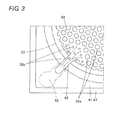
- the current flows through the extraction wiring 44, as shown with an arrow in Fig. 3 , between the fixed side electrode pad 45 and the fixed electrode film 40 with the change in electrostatic capacity between the diaphragm 33 and the fixed electrode film 40. Therefore, if the opening area of the acoustic hole 38b in the extraction wiring 44 and the region in the vicinity thereof is large, the cross-sectional area of the current passage becomes narrow and the parasitic resistance of the current passage becomes high. If the parasitic resistance becomes high, the electrical noise generated from the resistor body increases thus degrading the characteristics of the acoustic sensor.
- the opening area of the acoustic hole 38b formed in the extraction wiring 44 and in the region in the vicinity thereof is relatively small, and thus the cross-sectional area of the extraction wiring 44 and the current passage in the fixed electrode film 40 is less likely to become narrow by the acoustic hole 38b, and the parasitic resistance of the current flowing as shown with an arrow in Fig. 3 becomes smaller. Therefore, the parasitic resistance can be reduced and the noise can be reduced in the extraction wiring 44 and in the region of the vicinity thereof, and the S/N ratio of the sensor can be enhanced. As a result, the S/N ratio of the acoustic sensor 31 can be efficiently enhanced by the combination of the acoustic hole 38a having a relatively large opening area and the acoustic hole 38b having a relatively small opening area.
- the portion of the extraction wiring 44 has a narrow width and thus has low strength, where the strength further lowers as the acoustic hole 38b is opened.
- the tip of the extraction wiring 44 is fixed to the base part 41, so that stress easily concentrates at an area connected to the extraction wiring 44 of the fixed electrode film 40 and the strength also lowers by the acoustic hole 38b. Therefore, if the acoustic hole of a large opening area is formed, the extraction wiring 44 or the fixed electrode film 40 may break or disconnect at the extraction wiring 44 or the region in the vicinity thereof, and the acoustic sensor 31 may stop its function.
- the opening area of the acoustic hole 38b is formed small in the extraction wiring 44 and in the region in the vicinity thereof, so that the lowering of strength caused by the acoustic hole 38b in the extraction wiring 44 and in the region in the vicinity thereof can be reduced. Therefore, in the acoustic sensor 31, disconnection and breakage are less likely to occur in the extraction wiring 44 and the fixed electrode film 40, and the mechanical strength of the acoustic sensor 31 enhances.
- the acoustic holes 38a, 38b are substantially circular openings and are regularly arrayed.
- the acoustic hole 38a having a relatively large opening area in the region distant from the extraction wiring 44 will be described, As shown in Fig. 4 , the array pitch (inter-center distance) of the acoustic hole 38a is Wa + Da, where Wa is the diameter of the acoustic hole 38a having a large opening area and Da is the spaced distance between the acoustic holes 38a.
- the spaced distance Da x the thickness of the fixed electrode film 40 represents the cross-sectional area of the current passage with respect to the current flowing between the acoustic holes 38a.
- the opening rate of the acoustic hole 38a is preferably set large in the region distant from the extraction wiring 44 to enhance the S/N ratio of the acoustic sensor 31.
- Diameter Wa > Spaced distance Da is desirable.
- the spaced distance Da between the acoustic holes 38a is desirably made as narrow as possible to efficiently escape the thermal noise generated in the air gap between the diaphragm 33 and the fixed electrode film 40.
- the spaced distance between the acoustic holes 38a is narrowed in excess, the strength of the back plate 34 may lack or the electrode area of the fixed electrode film 40 may reduce. Therefore, Da > 0.25 ⁇ Wa is preferable. Therefore, the spaced distance Da between the acoustic holes 38a is preferably as narrow as possible, but has a lower limit of 0.25Wa.
- the array pitch of the acoustic hole 38b is Wb + Db, where Wb is the diameter of the acoustic hole 38b having a small opening area and Db is the spaced distance between the acoustic holes 38b.
- the spaced distance Db x the thickness of the fixed electrode film 40 represents the cross-sectional area of the current passage with respect to the current flowing between the acoustic holes 38b.
- the spaced distance Db is to be greater than the radius of the acoustic hole 38b (e.g., Db > 0.5 x Wb) to have the fixed electrode film 40 sufficiently strong.
- the array pitch Wb + Db of the acoustic holes 38b in the extraction wiring 44 and the region in the vicinity thereof is preferably equal to the array pitch Wa + Da of the acoustic holes 38a in the region distant from the extraction wiring 44 to uniformly etch the sacrifice layer of the air gap.
- the area for forming the acoustic hole 38b having a small opening area is desirably one or more zones and five or less zones.
- the thermal noise of the air gap cannot be reduced and the S/N ratio of the acoustic sensor 31 may be degraded if six or more zones.
- a set of acoustic holes 38b arranged continuously is assumed as one section. For instance, in the example of Fig.
- the first section (I) includes one acoustic hole 38b including the extraction wiring 44
- the second section (II) includes three acoustic holes 38b (e.g., acoustic hole 38b positioned on a hexagon in which the distance from the acoustic hole 38b of the first section (I) to the corner is Wb + Db)
- the third section (III) includes five acoustic holes 38b (acoustic hole 38b positioned on a hexagon in which the distance from the acoustic hole 38b of the first section (I) to the corner is 2Wb + 2Db).
- the interval of the acoustic holes 38b is the same in all directions, and thus one section is defined in the direction the acoustic holes 38b are lined as much as possible.
- Fig. 5 is a plan view of an acoustic sensor 61 according to a second embodiment of the present invention.
- Fig. 6 is a plan view showing the acoustic sensor 61 in which the plate portion 39 is omitted, and also shows one part in an enlarged manner.
- the acoustic sensor 61 of the second embodiment has a structure substantially similar to the acoustic sensor 31 of the first embodiment other than that the diaphragm 33 and the back plate 34 are formed to a substantially square shape, and hence the same reference numerals are denoted for the portions of the same structure as the first embodiment in the figures and the description thereof will be omitted.
- the diaphragm 33 is formed to a substantially square shape in the acoustic sensor 61, where a beam 62 is extended in the diagonal direction from the four corners.
- the diaphragm 33 has the lower surface of each beam 62 supported by the anchor 37 arranged on the upper surface of the silicon substrate 32 by SiO 2 .
- the acoustic hole 38b having a small opening area is formed in the region in the vicinity of the extraction wiring 44 extended from the fixed electrode film 40, and the acoustic hole 38a having a large opening area is formed in the region distant from the extraction wiring 44.
- the acoustic holes 38b are arranged at the same array pitch as the acoustic holes 38a so as to form three sections.
- FIG. 7 is a plan view of an acoustic sensor 71 according to the third embodiment of the present invention.
- one or a plurality of acoustic holes 38b having a small opening area is formed in the extraction wiring 44, and only the acoustic hole 38b at the extraction wiring 44 is assumed as the acoustic hole having a small opening area.
- the acoustic holes 38a having a large opening area is regularly arrayed in the region other than the region where the extraction wiring 44 is passed.
- some of the acoustic holes 38a are omitted from the acoustic holes 38a arrayed regularly in the region in the vicinity of the extraction wiring 44, so that the number density of the acoustic holes 38a is smaller than in the region distant from the extraction wiring 44 so that the array pitch of the acoustic holes 38a is increased.
- the opening rate of the acoustic hole is made small by reducing the opening area of the acoustic hole 38b in the extraction wiring 44. Furthermore, the opening rate of the acoustic hole is made small by reducing the number density of the acoustic holes 38a in the region in the vicinity of the extraction wiring 44.
- Fig. 7 can be assumed that the acoustic hole 38b having a small opening area is provided at the extraction wiring 44 and the acoustic hole is not provided (i.e., opening rate is zero) in the region in the vicinity of the extraction wiring 44.
- the opening rate may be made small only in the region where the extraction wiring 44 is passed as described next.
- the opening rate is made small by providing the acoustic hole 38b having a small opening area in the extraction wiring 44.
- the acoustic hole 38a having a large opening area may be regularly arrayed in the region other than the region where the extraction wiring 44 is passed, so that the region in the vicinity of the extraction wiring 44 has an opening rate same as the region distant from the extraction wiring 44.
- FIG. 8 is a plan view of an acoustic sensor 81 according to a fourth embodiment of the present invention.
- the acoustic holes 38a are formed in the region other than the region where the extraction wiring 44 is passed.
- the acoustic holes 38a all have an opening area (i.e., opening size) of the same size.
- the acoustic holes 38a are regularly arrayed in the region distant from the extraction wiring 44 so that the spaced distance between adjacent acoustic holes 38a becomes relatively small in the region distant from the extraction wiring 44.
- the acoustic holes 38a are arranged irregularly or at random in the region in the vicinity of the extraction wiring 44 so that the spaced distance between the acoustic holes 38a becomes greater in the region in the vicinity of the extraction wiring 44 than in the region distant from the extraction wiring 44.
- the opening rate is zero since the acoustic hole is not provided at the extraction wiring 44, and the number density of the acoustic hole 38a is small and the opening rate thereof is smaller than the region distant from the extraction wiring 44 in the region in the vicinity of the extraction wiring 44.
- the small acoustic hole 38b may be provided at the extraction wiring 44.
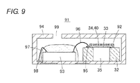
- Fig. 9 is a schematic cross-sectional view showing a microphone 91 according to a fifth embodiment of the present invention.
- an acoustic sensor 92 is mounted in a package 94 along with an IC circuit 93 (signal processing circuit), where an electrode pad 95 of the acoustic sensor 92 and the IC circuit 93 are wire connected with a bonding wire 96, and the IC circuit 93 is wire connected to an electrode portion 98 of the package 94 with a bonding wire 97.
- An acoustic vibration introducing hole 99 for introducing the acoustic vibration into the package 94 is opened at the upper surface of the package 94.
- the acoustic vibration enters the package 94 from the acoustic vibration introducing hole 99, such acoustic vibration is detected by the acoustic sensor 92.
- the electrostatic capacitance between the diaphragm 33 and the fixed electrode film 40 changes by the acoustic vibration, and such change in electrostatic capacitance is output to the IC circuit 93 as an electrical signal.
- the IC circuit 93 performs a predetermined signal processing on the electrical signal output from the acoustic sensor 92 so that it can be output to the outside from the electrode portion 98.
Landscapes
- Engineering & Computer Science (AREA)
- Physics & Mathematics (AREA)
- Acoustics & Sound (AREA)
- Signal Processing (AREA)
- Computer Hardware Design (AREA)
- Microelectronics & Electronic Packaging (AREA)
- Pressure Sensors (AREA)
- Electrostatic, Electromagnetic, Magneto- Strictive, And Variable-Resistance Transducers (AREA)
- Details Of Audible-Bandwidth Transducers (AREA)
Abstract
Description
- The present invention relates to acoustic sensors and microphones, and specifically to an MEMS (Micro Electro Mechanical Systems) type acoustic sensor manufactured by using the MEMS technique, and a microphone using such acoustic sensor.
- A capacitance type acoustic sensor is dislosed in Japanese Patent Publication No.
4338395 2009-89097 - In such acoustic sensor, the opening size of the acoustic hole needs to be made large to enhance the S/N ratio. However, the acoustic hole that is opened in the back plate is opened not only at the plate portion having a relatively thick film thickness but also at the fixed electrode film having a thin thickness. Therefore, if the opening size of the acoustic hole is made large, the extraction wiring portion of the fixed electrode film may easily break or the parasitic resistance may increase.
- The present invention has been devised to solve the problems described above, and an object thereof is to provide an acoustic sensor in which the fixed electrode film is less likely to break and the parasitic resistance is less likely to increase even if the opening size of the acoustic hole (acoustic perforation) opened in the back plate is made large.
- In accordance with one aspect of the present invention, there is provided an acoustic sensor including: a semiconductor substrate including a back chamber; a conductive diaphragm arranged on an upper side of the semiconductor substrate; an insulating fixed film fixed on an upper surface of the semiconductor substrate to cover the diaphragm with a gap; a conductive fixed electrode film arranged on the fixed film at a position facing the diaphragm; an extraction wiring extracted from the fixed electrode film; and an electrode pad, to which the extraction wiring is connected; the acoustic sensor converting an acoustic vibration to change in electrostatic capacitance between the diaphragm and the fixed electrode film; wherein a plurality of acoustic perforations is opened in a back plate including the fixed film and the fixed electrode film; and an opening rate of the acoustic perforation is smaller in the extraction wiring and a region in the vicinity thereof than in other regions.
- The opening rate is the ratio of the total of the opening area of the acoustic perforations with respect to the area of the region in the relevant region of an extent including a plurality of acoustic perforations. In order to reduce the opening rate of the acoustic perforations arranged in the extraction wiring and the region in the vicinity of the extraction wiring, the opening area per one acoustic perforation is to be reduced compared to other regions in the extraction wiring and the region in the vicinity of the extraction wiring. Alternatively, the inter-center distance between the adjacent acoustic perforations is made longer than other regions in the extraction wiring and the region in the vicinity of the extraction wiring.
- If the extraction wiring and the region in the vicinity of the extraction wiring includes an acoustic perforation having a smaller opening rate than the acoustic perforation in other regions, this includes a case where the extraction wiring or the region in the vicinity of the extraction wiring does not include the acoustic perforations (i.e., opening rate is zero).
- The region in the vicinity of the extraction wiring refers to the region within six times and preferably the region within substantially three times the average inter-center distance of the acoustic perforation measured from the basal end of the extraction wiring of the acoustic perforation formed region (excluding the region where the extraction wiring passes) of the back plate.
- In a first acoustic sensor of the present invention, the acoustic perforation in the extraction wiring and in the region in the vicinity thereof has a relatively small opening rate, and hence the width of the electrode film between the acoustic perforations in the extraction wiring and in the region in the vicinity thereof is less likely to become narrow and the parasitic resistance in the extraction wiring and in the region in the vicinity thereof can be reduced. Therefore, the generation of noise in the extraction wiring and in the region in the vicinity thereof can be reduced and the S/N ratio of the acoustic sensor can be enhanced. Furthermore, the width of the electrode film between the acoustic perforations can be widened in the extraction wiring and in the region in the vicinity thereof, so that the lowering of the strength of the fixed electrode film by the acoustic perforation in the extraction wiring and in the region in the vicinity thereof can be reduced. Therefore, the mechanical strength of the extraction wiring and the fixed electrode film increase, so that disconnection and breakage are less likely to occur.
- In the first acoustic sensor of the present invention, the opening rate of the acoustic perforation is relatively large in other regions excluding the extraction wiring and the vicinity thereof so that the acoustic vibration easily passes through the acoustic perforation, and the S/N ratio of the acoustic sensor is increased to enhance the sensitivity.
- One embodiment of the first acoustic sensor according to the present invention has the acoustic perforation arranged in the extraction wiring and the region in the vicinity of the extraction wiring, and the acoustic perforation in other regions excluding the extraction wiring and the region in the vicinity thereof arrayed according to the same rule. When referring to being arrayed according to the same rule, this means that the form of array (e.g., square arrangement and concentric arrangement, honeycomb arrangement, zigzag arrangement etc.) and the array pitch (inter-center distance between the acoustic perforations) are the same. According to such embodiment, the sacrifice layer of the air gap can be uniformly etched in the manufacturing step.
- in the above aspect, a diameter of the acoustic perforation having a relatively small opening area arranged in the extraction wiring or the region in the vicinity of the extraction wiring is smaller than twice a spaced distance between the acoustic perforations. According to such embodiment, the strength of the fixed electrode film can be ensured and the parasitic resistance can be reduced.
- In the above aspect, a diameter of the acoustic perforation having a relatively large opening area arranged in other regions excluding the extraction wiring and the region in the vicinity of the extraction wiring is greater than a spaced distance between the acoustic perforations. According to such embodiment, the S/N ratio of the acoustic sensor can be enhanced since the opening rate of the acoustic perforation becomes large in other regions excluding the extraction wiring and the region in the vicinity of the extraction wiring.
- In the above aspect, a diameter of the acoustic perforation having a relatively large opening area arranged in other regions excluding the extraction wiring and the region in the vicinity of the extraction wiring is smaller than four times a spaced distance between the acoustic perforations. According to such embodiment, the strength of the back plate can be prevented from lacking by making the opening area of the acoustic perforation too large, and the electrode area of the fixed electrode film can be prevented from becoming too small.
- In the above aspect, an inter-center distance between the adjacent acoustic perforations of the acoustic perforations having a relatively small opening area arrayed in the extraction wiring and the region in the vicinity of the extracting wiring is equal to an inter-center distance between the adjacent acoustic perforations of the acoustic perforations having a relatively large opening area arranged in other regions excluding the extraction wiring and the region in the vicinity of the extraction wiring. According to such embodiment, the sacrifice layer of the air gap can be uniformly etched in the manufacturing step.
- In the above aspect, the acoustic perforation contained in five or less zones including the acoustic perforation of the extraction wiring when counting from the acoustic perforation arranged at the extraction wiring is the acoustic perforation having a relatively small opening area. When referring to zones, this refers to the virtual line passing through the centers of a plurality of acoustic perforations at substantially equal distance from the extraction wiring. According to such embodiment, the strength of the back plate can be ensured and the parasitic resistance can be reduced.
- In accordance with another aspect of the present invention, there is provided an acoustic sensor including: a semiconductor substrate including a back chamber; a conductive diaphragm arranged on an upper side of the semiconductor substrate; an insulating fixed film fixed on an upper surface of the semiconductor substrate to cover the diaphragm with a gap; a conductive fixed electrode film arranged on the fixed film at a position facing the diaphragm; an extraction wiring extracted from the fixed electrode film; and an electrode pad, to which the extraction wiring is connected; the acoustic sensor converting an acoustic vibration to change in electrostatic capacitance between the diaphragm and the fixed electrode film; wherein a plurality of acoustic perforations is opened in a back plate including the fixed film and the fixed electrode film; and at least the extraction wiring, of the extraction wiring and a region in the vicinity of thereof, does not include the acoustic perforation or includes an acoustic perforation of small opening rate compared to an acoustic perforation arranged in other regions (excluding a case in which an acoustic perforation is not arranged in the extraction wiring, and an opening rate of an acoustic perforation arranged in the region in the vicinity of the extraction wiring and an opening rate of an acoustic perforation arranged in other regions excluding the extraction wiring and the region in the vicinity of the extraction wiring are equal).
- The opening rate is the ratio of the total of the opening area of the acoustic perforations with respect to the area of the region in the relevant region of an extent including a plurality of acoustic perforations. In order to reduce the opening rate of the acoustic perforations arranged in at least the extraction wiring of the extraction wiring and the region in the vicinity of the extraction wiring, the opening area per one acoustic perforation is to be reduced compared to the acoustic perforation in other regions excluding the extraction wiring and the region in the vicinity of the extraction wiring. Alternatively, the inter-center distance between the adjacent acoustic perforations is made longer than the acoustic perforation in other regions excluding the extraction wiring and the region in the vicinity of the extraction wiring.
- The region in the vicinity of the extraction wiring refers to the region within six times and preferably the region within substantially three times the average inter-center distance of the acoustic perforation measured from the basal end of the extraction wiring of the acoustic perforation formed region (excluding the region where the extraction wiring passes) of the back plate.
- In a second acoustic sensor of the present invention, the acoustic perforation in the extraction wiring and in the region in the vicinity thereof has a relatively small opening rate, or does the acoustic perforation is not provided, and hence the width of the electrode film between the acoustic perforations in the extraction wiring and in the region in the vicinity thereof is less likely to become narrow and the parasitic resistance in the extraction wiring and in the region in the vicinity thereof can be reduced. Therefore, the generation of noise in the extraction wiring and in the region in the vicinity thereof can be reduced and the S/N ratio of the acoustic sensor can be enhanced. Furthermore, the width of the electrode film between the acoustic perforations can be widened in the extraction wiring and in the region in the vicinity thereof, so that the lowering of the strength of the fixed electrode film by the acoustic perforation in the extraction wiring and in the region in the vicinity thereof can be reduced. Therefore, the mechanical strength of the extraction wiring and the fixed electrode film increase, so that disconnection and breakage are less likely to occur.
- In the second acoustic sensor of the present invention, the opening rate of the acoustic perforation is relatively large in other regions excluding the extraction wiring and the vicinity thereof so that the acoustic vibration easily passes through the acoustic perforation, and the S/N ratio of the acoustic sensor is increased to enhance the sensitivity.
- A first microphone according to the present invention has a first acoustic sensor according to the present invention and a signal processing circuit for processing an electrical signal output from the acoustic sensor accommodated in a housing. According to the microphone of the present invention, the generation of noise can be reduced and the S/N ratio of the microphone can be enhanced since the acoustic sensor of the present invention is used. Furthermore, the disconnection and breakage of the extraction wiring and the fixed electrode film in the acoustic sensor are less likely to occur, and the failure of the microphone is less likely to occur.
- A second microphone according to the present invention has a second acoustic sensor according to the present invention and a signal processing circuit for processing an electrical signal output from the acoustic sensor accommodated in a housing. According to the microphone of the present invention, the generation of noise can be reduced and the S/N ratio of the microphone can be enhanced since the acoustic sensor of the present invention is used. Furthermore, the disconnection and breakage of the extraction wiring and the fixed electrode film in the acoustic sensor are less likely to occur, and the failure of the microphone is less likely to occur.
- The means for solving the problems of the invention has a characteristic of appropriately combining the configuring elements described above, and the present invention enables a great number of variations by the combination of the configuring elements.
-
-
Fig. 1 is a plan view of an acoustic sensor according to a first embodiment of the present invention; -
Fig. 2 is a cross-sectional view taken along line X-X ofFig. 1 ; -
Fig. 3 is an operation explanatory view of the acoustic sensor of the first embodiment; -
Fig. 4 is a view describing the arrangement of acoustic holes in the acoustic sensor of the first embodiment; -
Fig. 5 is a plan view of an acoustic sensor according to a second embodiment of the present invention; -
Fig. 6 is a plan view of a state in which the plate portion of the back pilate is removed in the acoustic sensor of the second embodiment; -
Fig. 7 is a plan view of an acoustic sensor according to a third embodiment of the present invention; -
Fig. 8 is a plan view of an acoustic sensor according to a fourth embodiment of the present invention; and -
Fig. 9 is a schematic cross-sectional view of a microphone according to a fifth embodiment of the present invention. - Hereinafter, preferred embodiments of the present invention will be described with reference to the accompanied drawings. It should be noted that the present invention is not limited to the following embodiments and that various design changes can be made within a scope not deviating from the gist of the present invention.
- First, a structure of an
acoustic sensor 31 according to a first embodiment of the present invention will be described with reference toFig. 1 andFig. 2 .Fig. 1 is a plan view of theacoustic sensor 31.Fig. 2 is a cross-sectional view in a diagonal direction of the acoustic sensor 31 (cross-section taken along line X-X ofFig. 1 ). - The
acoustic sensor 31 is a capacitance type element manufactured by using the MEMS technique. As shown inFig. 2 , adiaphragm 33 is arranged on an upper surface of a silicon substrate 32 (semiconductor substrate) by way of ananchor 37, and aback plate 34 is fixed thereon by way of a microscopic air gap. - The
silicon substrate 32 made of monocrystalline silicon is formed with aback chamber 35 passed through from the front surface to the back surface. The inner peripheral surface of theback chamber 35 may be a perpendicular surface or may be inclined to a tapered shape. - A plurality of
anchors 37 for supporting the lower surface of the outer peripheral part of thediaphragm 33 is arranged on the upper surface of thesilicon substrate 32, and abase part 41 of thick film is formed on the upper surface of thesilicon substrate 32 to surround thediaphragm 33. Furthermore, the region on the outer side than thebase part 41 in the upper surface of thesilicon substrate 32 is covered with an adheringlayer 47 thinner than thebase part 41. Theanchor 37 and thebase part 41 are formed by SiO2. The adheringlayer 47 is made by SiO2 or polysilicon. - As shown in
Fig. 1 , thediaphragm 33 is formed by a substantially circular plate shaped polysilicon thin firm, and has conductivity. A band plate shapedextraction wiring 43 is extended towards the outer side from thediaphragm 33. - The
diaphragm 33 is arranged on thesilicon substrate 32 so as to cover the opening in the upper surface of theback chamber 35, The entire periphery of the lower surface at the outer peripheral part of the diaphragm 33' is fixed to the upper surface of thesilicon substrate 32 by theanchor 37. Therefore, thediaphragm 33 floats in air at the upper side of thechamber 35, and can film vibrate sympathized to the acoustic vibration (air vibration). - In the
back plate 34, a fixedelectrode film 40 made of polysilicon is arranged at the lower surface of a plate portion 39 (fixed film) made of nitride film (SiN). Theback plate 34 has a canopy shape, and covers thediaphragm 33 at the hollow portion underneath. The height of the hollow portion under the back plate 34 (height from the upper surface of thesilicon substrate 32 to the lower surface of the fixed electrode film 40) is equal to the thickness of thebase part 41 formed on the upper surface of thesilicon substrate 32 due to manufacturing reasons. A microscopic air gap is formed between the lower surface of the back plate 34 (i.e., lower surface of the fixed electrode film 40) and the upper surface of thediaphragm 33. The fixedelectrode film 40 faces thediaphragm 33, which is a movable electrode fllm, and configures a capacitor. - A great number of
acoustic holes back plate 34 so as to pass from the upper surface to the lower surface. Theacoustic hole 38b formed in theextraction wiring 44 of the fixedelectrode film 40 and the region in the vicinity thereof in theback plate 34 has a smaller opening area than theacoustic hole 38a formed in other regions (i.e., majority of the region distant from theextraction wiring 44 of the acoustic perforation formed region of the back plate 34). Theacoustic holes plate portion 39 to the fixedelectrode film 40, where the acoustic hole of theplate portion 39 and the acoustic hole of the fixedelectrode film 40 are denoted with the same reference number. - A small gap (passage of acoustic vibration) is formed between the lower surface of the outer peripheral part of the
diaphragm 33 and the upper surface of thesilicon substrate 32. Therefore, the acoustic vibration that entered theback plate 34 through theacoustic holes diaphragm 33 and exits to theback chamber 35 through the gap between the outer peripheral part of thediaphragm 33 and thesilicon substrate 32. - A great number of
microscopic stoppers 42 is projected at the inner surface of theback plate 34, so that thediaphragm 33 is prevented from being adsorbed to the lower surface of theback plate 34 and not being able to return by the electrostatic attractive force of when excess voltage is applied between thediaphragm 33 and the fixedelectrode film 40. A phenomenon in which thediaphragm 33 fixes (sticks) to theback plate 34 and does not return due to the moisture that entered between thediaphragm 33 and theback plate 34 is also prevented by thestopper 42. - A
protective film 53 is continuously extended over the entire periphery from the outer peripheral edge of the canopy shapedplate portion 39. Therefore, theprotective film 53 is formed by a nitride film (SiN) same as theplate portion 39, and has substantially the same film thickness as theplate portion 39. The inner peripheral part of theprotective film 53 is abase covering part 51 having a reverse groove shaped cross-section, and the outer peripheral part of theprotective film 53 is aflat part 52. - The
back plate 34 is fixed to the upper surface of thesilicon substrate 32, and theprotective film 53 covers the outer peripheral part of the upper surface of thesilicon substrate 32 with thebase part 41 and the adheringlayer 47 interposed. Thebase covering part 51 of theprotective film 53 covers thebase part 41, and theflat part 52 covers the upper surface of the adheringlayer 47, - The
extraction wiring 43 of thediaphragm 33 is fixed to thebase part 41, and theextraction wiring 44 extended from the fixedelectrode film 40 is also fixed to the upper surface of thebase part 41. An opening is formed in thebase covering part 51, a movable side electrode pad 46 (electrode terminal) is formed on the upper surface of theextraction wiring 43 through the opening, and the movableside electrode pad 46 is conducted to the extraction wiring 43 (therefore, to the diaphragm 33). A fixed side electrode pad 45 (electrode terminal) arranged on the upper surface of theplate portion 39 is conducted to the extraction wiring 44 (therefore, to the fixed electrode film 40) through a through hole and the like. - The
acoustic hole 38b arranged in theextraction wiring 44 or the region of in the vicinity thereof has a relatively small opening area, and theacoustic hole 38a formed in other regions has a relatively large opening area. Theacoustic holes Fig. 1 , or may be arrayed to a square shape or a circular ring shape, or may be arrayed at random. Therefore, the spaced distance between theacoustic holes 38a (i.e., shortest distance between the outer peripheries of the adjacent acoustic holes) is relatively small in the region where theacoustic hole 38a of a large opening area is formed, and the spaced distance between theacoustic holes 38b is relatively large in the region where theacoustic hole 38b of a small opening area is formed. - Furthermore, in the
acoustic sensor 31, when the acoustic vibration passes through theacoustic holes back plate 34 and thediaphragm 33, thediaphragm 33 or the thin film resonates to the acoustic vibration and film vibrates. When thediaphragm 33 vibrates and the gap distance between thediaphragm 33 and the fixedelectrode film 40 changes, the electrostatic capacitance between thediaphragm 33 and the fixedelectrode film 40 changes. As a result, in theacoustic sensor 31, the acoustic vibration (change in sound pressure) sensed by thediaphragm 33 becomes the change in the electrostatic capacitance between thediaphragm 33 and the fixedelectrode film 40, and is output from theelectrodes pads - In the
acoustic sensor 31, theacoustic hole 38a having a relatively large opening area is formed in the region excluding theextraction wiring 44 and the region in the vicinity of theextraction wiring 44, that is, the majority of theback plate 34, and thus the acoustic vibration easily passes theacoustic holes acoustic sensor 31 becomes large thus enhancing the sensitivity. - However, the current flows through the
extraction wiring 44, as shown with an arrow inFig. 3 , between the fixedside electrode pad 45 and the fixedelectrode film 40 with the change in electrostatic capacity between thediaphragm 33 and the fixedelectrode film 40. Therefore, if the opening area of theacoustic hole 38b in theextraction wiring 44 and the region in the vicinity thereof is large, the cross-sectional area of the current passage becomes narrow and the parasitic resistance of the current passage becomes high. If the parasitic resistance becomes high, the electrical noise generated from the resistor body increases thus degrading the characteristics of the acoustic sensor. - In the
acoustic sensor 31, on the other hand, the opening area of theacoustic hole 38b formed in theextraction wiring 44 and in the region in the vicinity thereof is relatively small, and thus the cross-sectional area of theextraction wiring 44 and the current passage in the fixedelectrode film 40 is less likely to become narrow by theacoustic hole 38b, and the parasitic resistance of the current flowing as shown with an arrow inFig. 3 becomes smaller. Therefore, the parasitic resistance can be reduced and the noise can be reduced in theextraction wiring 44 and in the region of the vicinity thereof, and the S/N ratio of the sensor can be enhanced. As a result, the S/N ratio of theacoustic sensor 31 can be efficiently enhanced by the combination of theacoustic hole 38a having a relatively large opening area and theacoustic hole 38b having a relatively small opening area. - The portion of the
extraction wiring 44 has a narrow width and thus has low strength, where the strength further lowers as theacoustic hole 38b is opened. The tip of theextraction wiring 44 is fixed to thebase part 41, so that stress easily concentrates at an area connected to theextraction wiring 44 of the fixedelectrode film 40 and the strength also lowers by theacoustic hole 38b. Therefore, if the acoustic hole of a large opening area is formed, theextraction wiring 44 or the fixedelectrode film 40 may break or disconnect at theextraction wiring 44 or the region in the vicinity thereof, and theacoustic sensor 31 may stop its function. - In the
acoustic sensor 31, on the other hand, the opening area of theacoustic hole 38b is formed small in theextraction wiring 44 and in the region in the vicinity thereof, so that the lowering of strength caused by theacoustic hole 38b in theextraction wiring 44 and in the region in the vicinity thereof can be reduced. Therefore, in theacoustic sensor 31, disconnection and breakage are less likely to occur in theextraction wiring 44 and the fixedelectrode film 40, and the mechanical strength of theacoustic sensor 31 enhances. - The relationship between the size and the pitch of the
acoustic holes acoustic sensor 31 will now be described. Theacoustic holes - The
acoustic hole 38a having a relatively large opening area in the region distant from theextraction wiring 44 will be described, As shown inFig. 4 , the array pitch (inter-center distance) of theacoustic hole 38a is Wa + Da, where Wa is the diameter of theacoustic hole 38a having a large opening area and Da is the spaced distance between theacoustic holes 38a. The spaced distance Da x the thickness of the fixedelectrode film 40 represents the cross-sectional area of the current passage with respect to the current flowing between theacoustic holes 38a. - First of all, the opening rate of the
acoustic hole 38a is preferably set large in the region distant from theextraction wiring 44 to enhance the S/N ratio of theacoustic sensor 31.
Diameter Wa > Spaced distance Da is desirable. - The spaced distance Da between the
acoustic holes 38a is desirably made as narrow as possible to efficiently escape the thermal noise generated in the air gap between thediaphragm 33 and the fixedelectrode film 40. However, if the spaced distance between theacoustic holes 38a is narrowed in excess, the strength of theback plate 34 may lack or the electrode area of the fixedelectrode film 40 may reduce. Therefore,
is preferable. Therefore, the spaced distance Da between theacoustic holes 38a is preferably as narrow as possible, but has a lower limit of 0.25Wa. - Summarizing the above, the condition
0.25 x Wa < Da < Wa is obtained. - If the diameter Wa of the
acoustic hole 38a is excessively small, the sacrifice layer present in theback plate 34 may not be etched in the manufacturing step or thermal noise may generate inside theacoustic hole 38a. The diameter Wa of theacoustic hole 38a is desirably greater than or equal to 3 µm. For instance, if Wa = 16 µm and Da = 8 µm, the thermal noise in the air gap becomes small and high S/N ratio can be obtained. - The
acoustic hole 38b having a relatively small opening area in theextraction wiring 44 and the region in the vicinity thereof will now be described. As shown inFig. 4 , the array pitch of theacoustic hole 38b is Wb + Db, where Wb is the diameter of theacoustic hole 38b having a small opening area and Db is the spaced distance between theacoustic holes 38b. The spaced distance Db x the thickness of the fixedelectrode film 40 represents the cross-sectional area of the current passage with respect to the current flowing between theacoustic holes 38b. - The ensuring of the strength of the fixed
electrode film 40 and the reduction of the parasitic resistance need to be prioritized in the vicinity of theextraction wiring 44, and thus the spaced distance Db between theacoustic holes 38b is desirably wide. In particular, the spaced distance Db is to be greater than the radius of theacoustic hole 38b (e.g., Db > 0.5 x Wb) to have the fixedelectrode film 40 sufficiently strong. The array pitch Wb + Db of theacoustic holes 38b in theextraction wiring 44 and the region in the vicinity thereof is preferably equal to the array pitch Wa + Da of theacoustic holes 38a in the region distant from theextraction wiring 44 to uniformly etch the sacrifice layer of the air gap. That is, Da < Db since Wa > Wb when Wb + Db = Wa + Da. Therefore, if the arrangement of theacoustic hole 38a is such that Wa = 16 µm and Da = 8 µm, the fixedelectrode film 40 can have sufficient strength and the sacrifice layer can be uniformly etched if the arrangement of theacoustic holes 38b is Wb = 10 µm and Db = 14 µm. - From the standpoint of ensuring the strength of the
back plate 34 and reducing the parasitic resistance, the area for forming theacoustic hole 38b having a small opening area is desirably one or more zones and five or less zones. The thermal noise of the air gap cannot be reduced and the S/N ratio of theacoustic sensor 31 may be degraded if six or more zones. With regards to the section of theacoustic hole 38b, a set ofacoustic holes 38b arranged continuously (in particular, lined in short interval and assumed as continuous) is assumed as one section. For instance, in the example ofFig. 4 , three sections are provided, where the first section (I) includes oneacoustic hole 38b including theextraction wiring 44, the second section (II) includes threeacoustic holes 38b (e.g.,acoustic hole 38b positioned on a hexagon in which the distance from theacoustic hole 38b of the first section (I) to the corner is Wb + Db), and the third section (III) includes fiveacoustic holes 38b (acoustic hole 38b positioned on a hexagon in which the distance from theacoustic hole 38b of the first section (I) to the corner is 2Wb + 2Db). In the example ofFig. 4 , the interval of theacoustic holes 38b is the same in all directions, and thus one section is defined in the direction theacoustic holes 38b are lined as much as possible. - An acoustic sensor according to a second embodiment of the present invention will be described.
Fig. 5 is a plan view of anacoustic sensor 61 according to a second embodiment of the present invention.Fig. 6 is a plan view showing theacoustic sensor 61 in which theplate portion 39 is omitted, and also shows one part in an enlarged manner. - The
acoustic sensor 61 of the second embodiment has a structure substantially similar to theacoustic sensor 31 of the first embodiment other than that thediaphragm 33 and theback plate 34 are formed to a substantially square shape, and hence the same reference numerals are denoted for the portions of the same structure as the first embodiment in the figures and the description thereof will be omitted. - As shown in
Fig. 6 , thediaphragm 33 is formed to a substantially square shape in theacoustic sensor 61, where abeam 62 is extended in the diagonal direction from the four corners. Thediaphragm 33 has the lower surface of eachbeam 62 supported by theanchor 37 arranged on the upper surface of thesilicon substrate 32 by SiO2. - In the
acoustic sensor 61 as well, theacoustic hole 38b having a small opening area is formed in the region in the vicinity of theextraction wiring 44 extended from the fixedelectrode film 40, and theacoustic hole 38a having a large opening area is formed in the region distant from theextraction wiring 44. Theacoustic holes 38b are arranged at the same array pitch as theacoustic holes 38a so as to form three sections. - An acoustic sensor according to a third embodiment of the present invention will now be described.
Fig. 7 is a plan view of anacoustic sensor 71 according to the third embodiment of the present invention. - In the
acoustic sensor 71 of the third embodiment, one or a plurality ofacoustic holes 38b having a small opening area is formed in theextraction wiring 44, and only theacoustic hole 38b at theextraction wiring 44 is assumed as the acoustic hole having a small opening area. Theacoustic holes 38a having a large opening area is regularly arrayed in the region other than the region where theextraction wiring 44 is passed. However, some of theacoustic holes 38a are omitted from theacoustic holes 38a arrayed regularly in the region in the vicinity of theextraction wiring 44, so that the number density of theacoustic holes 38a is smaller than in the region distant from theextraction wiring 44 so that the array pitch of theacoustic holes 38a is increased. - In the present embodiment, the opening rate of the acoustic hole is made small by reducing the opening area of the
acoustic hole 38b in theextraction wiring 44. Furthermore, the opening rate of the acoustic hole is made small by reducing the number density of theacoustic holes 38a in the region in the vicinity of theextraction wiring 44. - The embodiment of
Fig. 7 can be assumed that theacoustic hole 38b having a small opening area is provided at theextraction wiring 44 and the acoustic hole is not provided (i.e., opening rate is zero) in the region in the vicinity of theextraction wiring 44. - Furthermore, the opening rate may be made small only in the region where the
extraction wiring 44 is passed as described next. In other words, the opening rate is made small by providing theacoustic hole 38b having a small opening area in theextraction wiring 44. Theacoustic hole 38a having a large opening area may be regularly arrayed in the region other than the region where theextraction wiring 44 is passed, so that the region in the vicinity of theextraction wiring 44 has an opening rate same as the region distant from theextraction wiring 44. - An acoustic sensor according to a fourth embodiment of the present invention will be described.
Fig. 8 is a plan view of anacoustic sensor 81 according to a fourth embodiment of the present invention. - In the
acoustic sensor 81 of the fourth embodiment, theacoustic holes 38a are formed in the region other than the region where theextraction wiring 44 is passed. Theacoustic holes 38a all have an opening area (i.e., opening size) of the same size. Theacoustic holes 38a are regularly arrayed in the region distant from theextraction wiring 44 so that the spaced distance between adjacentacoustic holes 38a becomes relatively small in the region distant from theextraction wiring 44. Theacoustic holes 38a are arranged irregularly or at random in the region in the vicinity of theextraction wiring 44 so that the spaced distance between theacoustic holes 38a becomes greater in the region in the vicinity of theextraction wiring 44 than in the region distant from theextraction wiring 44. - In the present embodiment, the opening rate is zero since the acoustic hole is not provided at the
extraction wiring 44, and the number density of theacoustic hole 38a is small and the opening rate thereof is smaller than the region distant from theextraction wiring 44 in the region in the vicinity of theextraction wiring 44. - In the embodiment of
Fig. 8 , the smallacoustic hole 38b may be provided at theextraction wiring 44. -
Fig. 9 is a schematic cross-sectional view showing amicrophone 91 according to a fifth embodiment of the present invention. As shown inFig. 9 , anacoustic sensor 92 is mounted in apackage 94 along with an IC circuit 93 (signal processing circuit), where anelectrode pad 95 of theacoustic sensor 92 and theIC circuit 93 are wire connected with abonding wire 96, and theIC circuit 93 is wire connected to anelectrode portion 98 of thepackage 94 with abonding wire 97. An acousticvibration introducing hole 99 for introducing the acoustic vibration into thepackage 94 is opened at the upper surface of thepackage 94. - Therefore, when the acoustic vibration enters the
package 94 from the acousticvibration introducing hole 99, such acoustic vibration is detected by theacoustic sensor 92. The electrostatic capacitance between thediaphragm 33 and the fixedelectrode film 40 changes by the acoustic vibration, and such change in electrostatic capacitance is output to theIC circuit 93 as an electrical signal. TheIC circuit 93 performs a predetermined signal processing on the electrical signal output from theacoustic sensor 92 so that it can be output to the outside from theelectrode portion 98.
Claims (11)
- An acoustic sensor (31, 61) comprising:a semiconductor substrate (32) including a back chamber (35);a conductive diaphragm (33) arranged on an upper side of the semiconductor substrate (32);an insulating fixed film (39) fixed on an upper surface of the semiconductor substrate (32) to cover the diaphragm (33) with a gap;a conductive fixed electrode film (40) arranged on the fixed film (39) at a position facing the diaphragm (33);an extraction wiring (44) extracted from the fixed electrode film (40); andan electrode pad, to which the extraction wiring (44) is connected;the acoustic sensor (31, 61) converting an acoustic vibration to change in electrostatic capacitance between the diaphragm (33) and the fixed electrode film (40); characterized in thata plurality of acoustic perforations (38a, 38b) is opened in a back plate (34) including the fixed film (39) and the fixed electrode film (40); andan opening rate of the acoustic perforation (38a, 38b) is smaller in the extraction wiring (44) and a region in the vicinity thereof than in other regions.
- The acoustic sensor (31, 61) according to claim 1, characterized in that an opening area per one acoustic perforation (38a, 38b) is smaller in the extraction wiring (44) and a region in the vicinity thereof than in other regions.
- The acoustic sensor (31, 61) according to claim 1, characterized in that an inter-center distance between adjacent acoustic perforations (38a, 38b) is longer in the extraction wiring (44) and a region in the vicinity thereof than in other regions.
- The acoustic sensor (31, 61) according to claim 2, characterized in that the acoustic perforation (38a, 38b) arranged in the extraction wiring (44) and in the region in the vicinity of the extraction wiring (44), and the acoustic perforation (38a, 38b) in other regions excluding the extraction wiring (44) and in the region in the vicinity of the extraction wiring (44) are arrayed according to a same rule.
- The acoustic sensor (31, 61) according to claim 2, characterized in that a diameter of the acoustic perforation (38a, 38b) having a relatively small opening area arranged in the extraction wiring (44) or the region in the vicinity of the extraction wiring (44) is smaller than twice a spaced distance between the acoustic perforations (38a, 38b).
- The acoustic sensor (31, 61) according to claim 2, characterized in that a diameter of the acoustic perforation (38a, 38b) having a relatively large opening area arranged in other regions excluding the extraction wiring (44) and the region in the vicinity of the extraction wiring (44) is greater than a spaced distance between the acoustic perforations (38a, 38b).
- The acoustic sensor (31, 61) according to claim 2, characterized in that a diameter of the acoustic perforation (38a, 38b) having a relatively large opening area arranged in other regions excluding the extraction wiring (44) and the region in the vicinity of the extraction wiring (44) is smaller than four times a spaced distance between the acoustic perforations (38a, 38b).
- The acoustic sensor (31, 61) according to claim 2, characterized in that an inter-center distance between the adjacent acoustic perforations (38a, 38b) of the acoustic perforations (38a, 38b) having a relatively small opening area arrayed in the extraction wiring (44) and the region in the vicinity of the extracting wiring is equal to an inter-center distance between the adjacent acoustic perforations (38a, 38b) of the acoustic perforations (38a, 38b) having a relatively large opening area arranged in other regions excluding the extraction wiring (44) and the region in the vicinity of the extraction wiring (44).
- The acoustic sensor (31, 61) according to claim 2, characterized in that the acoustic perforation (38a, 38b) contained in five or less zones including the acoustic perforation (38a, 38b) of the extraction wiring (44) when counting from the acoustic perforation (38a, 38b) arranged at the extraction wiring (44) is the acoustic perforation (38a, 38b) having a relatively small opening area.
- An acoustic sensor (31, 61) according to claim 1, characterized in that
at least the extraction wiring (44), of the extraction wiring (44) and a region in the vicinity thereof, does not include the acoustic perforation (38a, 38b) or includes an acoustic perforation (38a, 38b) of small opening rate compared to an acoustic perforation (38a, 38b) arranged in other regions (excluding a case in which an acoustic perforation (38a, 38b) is not arranged in the extraction wiring (44), and an opening rate of an acoustic perforation (38a, 38b) arranged in the region in the vicinity of the extraction wiring (44) and an opening rate of an acoustic perforation (38a, 38b) arranged in other regions excluding the extraction wiring (44) and the region in the vicinity of the extraction wiring (44) are equal). - A microphone in which the acoustic sensor (31, 61) according to any of the preceding claims, and a signal processing circuit (93) for processing an electrical signal output from the acoustic sensor (31, 61) are accommodated in a housing.
Applications Claiming Priority (2)
| Application Number | Priority Date | Filing Date | Title |
|---|---|---|---|
| JP2010110945 | 2010-05-13 | ||
| JP2011074454A JP4947220B2 (en) | 2010-05-13 | 2011-03-30 | Acoustic sensor and microphone |
Publications (3)
| Publication Number | Publication Date |
|---|---|
| EP2387255A2 true EP2387255A2 (en) | 2011-11-16 |
| EP2387255A3 EP2387255A3 (en) | 2014-07-16 |
| EP2387255B1 EP2387255B1 (en) | 2017-08-16 |
Family
ID=44343716
Family Applications (1)
| Application Number | Title | Priority Date | Filing Date |
|---|---|---|---|
| EP11165749.0A Not-in-force EP2387255B1 (en) | 2010-05-13 | 2011-05-11 | Acoustic sensor and microphone |
Country Status (5)
| Country | Link |
|---|---|
| US (1) | US8542851B2 (en) |
| EP (1) | EP2387255B1 (en) |
| JP (1) | JP4947220B2 (en) |
| KR (1) | KR101265420B1 (en) |
| CN (1) | CN102244827B (en) |
Cited By (1)
| Publication number | Priority date | Publication date | Assignee | Title |
|---|---|---|---|---|
| KR101445655B1 (en) * | 2014-06-11 | 2014-10-06 | 범진시엔엘 주식회사 | Method for manufacturing diaphragm assembly for piezoelectric speaker |
Families Citing this family (40)
| Publication number | Priority date | Publication date | Assignee | Title |
|---|---|---|---|---|
| JP5454345B2 (en) * | 2010-05-11 | 2014-03-26 | オムロン株式会社 | Acoustic sensor and manufacturing method thereof |
| JP5861497B2 (en) * | 2012-02-29 | 2016-02-16 | オムロン株式会社 | Sensor device |
| JP5928163B2 (en) * | 2012-05-31 | 2016-06-01 | オムロン株式会社 | Capacitive sensor, acoustic sensor and microphone |
| US8872288B2 (en) | 2012-08-09 | 2014-10-28 | Infineon Technologies Ag | Apparatus comprising and a method for manufacturing an embedded MEMS device |
| JP6028479B2 (en) * | 2012-09-14 | 2016-11-16 | オムロン株式会社 | Capacitive sensor, acoustic sensor and microphone |
| US8987842B2 (en) * | 2012-09-14 | 2015-03-24 | Solid State System Co., Ltd. | Microelectromechanical system (MEMS) device and fabrication method thereof |
| JP6127595B2 (en) * | 2013-03-11 | 2017-05-17 | オムロン株式会社 | Acoustic transducer |
| US9809448B2 (en) | 2013-03-13 | 2017-11-07 | Invensense, Inc. | Systems and apparatus having MEMS acoustic sensors and other MEMS sensors and methods of fabrication of the same |
| US8692340B1 (en) * | 2013-03-13 | 2014-04-08 | Invensense, Inc. | MEMS acoustic sensor with integrated back cavity |
| JP6184282B2 (en) * | 2013-10-01 | 2017-08-23 | 株式会社オーディオテクニカ | Capacitor headphone unit and method of manufacturing capacitor headphone fixed pole assembly |
| KR101514332B1 (en) * | 2013-11-05 | 2015-04-22 | (주)파트론 | Microphone package and manufacturing method thereof |
| US10322481B2 (en) | 2014-03-06 | 2019-06-18 | Infineon Technologies Ag | Support structure and method of forming a support structure |
| JP6252767B2 (en) * | 2014-03-14 | 2017-12-27 | オムロン株式会社 | Capacitive transducer |
| JP6311375B2 (en) * | 2014-03-14 | 2018-04-18 | オムロン株式会社 | Capacitive transducer |
| JP6481265B2 (en) * | 2014-06-18 | 2019-03-13 | 新日本無線株式会社 | MEMS element |
| US9503823B2 (en) * | 2014-12-24 | 2016-11-22 | Infineon Technologies Ag | Capacitive microphone with insulated conductive plate |
| CN105871249B (en) * | 2015-01-19 | 2019-12-31 | 北京纳米能源与系统研究所 | Acoustic-electric conversion component, charging device and sound signal collector using the same |
| KR101776725B1 (en) * | 2015-12-11 | 2017-09-08 | 현대자동차 주식회사 | Mems microphone and manufacturing method the same |
| JP6809008B2 (en) * | 2016-07-08 | 2021-01-06 | オムロン株式会社 | MEMS structure and capacitance type sensor, piezoelectric type sensor, acoustic sensor having MEMS structure |
| CN107690114B (en) * | 2016-08-04 | 2023-10-03 | 共达电声股份有限公司 | MEMS microphone vibrating diaphragm and MEMS microphone |
| KR101776752B1 (en) | 2016-09-02 | 2017-09-08 | 현대자동차 주식회사 | Microphone |
| KR101807071B1 (en) * | 2016-10-06 | 2017-12-08 | 현대자동차 주식회사 | Microphone and manufacturing method thereof |
| KR101781904B1 (en) * | 2017-08-14 | 2017-09-27 | 주식회사 신성씨앤티 | MEMS acoustic sensor |
| US11228845B2 (en) * | 2017-09-18 | 2022-01-18 | Knowles Electronics, Llc | Systems and methods for acoustic hole optimization |
| CN107484051B (en) * | 2017-09-29 | 2021-04-09 | 瑞声声学科技(深圳)有限公司 | MEMS microphone |
| JP7067891B2 (en) * | 2017-10-18 | 2022-05-16 | Mmiセミコンダクター株式会社 | Transducer |
| KR101938584B1 (en) * | 2017-10-20 | 2019-01-15 | 소스트 주식회사 | Mems microphone |
| KR102091854B1 (en) * | 2018-11-30 | 2020-03-20 | (주)다빛센스 | Condensor microphone and manufacturing method thereof |
| CN110603818B (en) * | 2018-12-29 | 2020-12-22 | 共达电声股份有限公司 | MEMS Sound Sensors, MEMS Microphones and Electronic Devices |
| CN113647118B (en) * | 2019-03-28 | 2024-03-08 | 住友理工株式会社 | Electrostatic transducers and electrostatic transducer units |
| US11729569B2 (en) * | 2019-10-10 | 2023-08-15 | Bose Corporation | Dimensional consistency of miniature loudspeakers |
| US11498830B2 (en) * | 2020-03-09 | 2022-11-15 | Solid State System Co., Ltd. | Structure of micro-electro-mechanical-system microphone and method for fabricating the same |
| CN114390415A (en) * | 2020-10-19 | 2022-04-22 | 瑶芯微电子科技(上海)有限公司 | MEMS microphone structure and manufacturing method thereof |
| CN114390414A (en) * | 2020-10-19 | 2022-04-22 | 瑶芯微电子科技(上海)有限公司 | MEMS microphone structure |
| KR20220080413A (en) * | 2020-12-07 | 2022-06-14 | 주식회사 디비하이텍 | MEMS microphone and method of manufacturing the same |
| KR102544661B1 (en) * | 2021-01-07 | 2023-06-20 | 주식회사 신성사운드모션 | MEMS acoustic sensor |
| US11805365B2 (en) * | 2021-03-24 | 2023-10-31 | Audeze, Llc | Electroacoustic diaphragm, transducer, audio device, and methods having subcircuits |
| CN113543002A (en) * | 2021-08-06 | 2021-10-22 | 瑶芯微电子科技(上海)有限公司 | MEMS microphone and back plate thereof |
| CN113573222A (en) * | 2021-08-06 | 2021-10-29 | 瑶芯微电子科技(上海)有限公司 | MEMS microphone and back plate thereof |
| JP2023142356A (en) | 2022-03-25 | 2023-10-05 | Mmiセミコンダクター株式会社 | MEMS microphone |
Citations (2)
| Publication number | Priority date | Publication date | Assignee | Title |
|---|---|---|---|---|
| JP2009089097A (en) | 2007-09-28 | 2009-04-23 | Yamaha Corp | Vibration transducer |
| JP4338395B2 (en) | 2000-08-11 | 2009-10-07 | ノールズ エレクトロニクス,リミテッド ライアビリティ カンパニー | Small broadband converter |
Family Cites Families (13)
| Publication number | Priority date | Publication date | Assignee | Title |
|---|---|---|---|---|
| FI115500B (en) * | 2000-03-21 | 2005-05-13 | Nokia Oyj | A method for manufacturing a membrane sensor |
| US6535460B2 (en) | 2000-08-11 | 2003-03-18 | Knowles Electronics, Llc | Miniature broadband acoustic transducer |
| JP2006121465A (en) * | 2004-10-22 | 2006-05-11 | Sanyo Electric Co Ltd | Acoustic sensor and method for manufacturing acoustic sensor |
| CN1802037B (en) * | 2005-09-29 | 2011-09-14 | 深圳市豪恩电声科技有限公司 | Back electret type silicon-based minisize electret capacitor microphone |
| JP2007104195A (en) * | 2005-10-03 | 2007-04-19 | Sharp Corp | Speaker device, display device, and perforated member |
| JP4567643B2 (en) | 2006-08-24 | 2010-10-20 | パナソニック株式会社 | Capacitor and manufacturing method thereof |
| US8121315B2 (en) | 2007-03-21 | 2012-02-21 | Goer Tek Inc. | Condenser microphone chip |
| CN101272636B (en) * | 2007-03-21 | 2012-07-18 | 歌尔声学股份有限公司 | Capacitor type microphone chip |
| JP5034692B2 (en) * | 2007-06-04 | 2012-09-26 | オムロン株式会社 | Acoustic sensor |
| DE102007029911A1 (en) * | 2007-06-28 | 2009-01-02 | Robert Bosch Gmbh | Acoustic sensor element |
| US20090136064A1 (en) | 2007-09-28 | 2009-05-28 | Yamaha Corporation | Vibration transducer and manufacturing method therefor |
| WO2009104389A1 (en) * | 2008-02-20 | 2009-08-27 | オムロン株式会社 | Electrostatic capacitive vibrating sensor |
| CN101644718B (en) * | 2009-07-02 | 2011-08-17 | 中国科学院声学研究所 | Capacitive acceleration sensor with acoustic cavity |
-
2011
- 2011-03-30 JP JP2011074454A patent/JP4947220B2/en not_active Expired - Fee Related
- 2011-05-02 KR KR1020110041609A patent/KR101265420B1/en not_active Expired - Fee Related
- 2011-05-11 EP EP11165749.0A patent/EP2387255B1/en not_active Not-in-force
- 2011-05-11 US US13/105,440 patent/US8542851B2/en active Active
- 2011-05-13 CN CN201110123632.3A patent/CN102244827B/en active Active
Patent Citations (2)
| Publication number | Priority date | Publication date | Assignee | Title |
|---|---|---|---|---|
| JP4338395B2 (en) | 2000-08-11 | 2009-10-07 | ノールズ エレクトロニクス,リミテッド ライアビリティ カンパニー | Small broadband converter |
| JP2009089097A (en) | 2007-09-28 | 2009-04-23 | Yamaha Corp | Vibration transducer |
Cited By (1)
| Publication number | Priority date | Publication date | Assignee | Title |
|---|---|---|---|---|
| KR101445655B1 (en) * | 2014-06-11 | 2014-10-06 | 범진시엔엘 주식회사 | Method for manufacturing diaphragm assembly for piezoelectric speaker |
Also Published As
| Publication number | Publication date |
|---|---|
| US8542851B2 (en) | 2013-09-24 |
| US20110280419A1 (en) | 2011-11-17 |
| JP4947220B2 (en) | 2012-06-06 |
| KR101265420B1 (en) | 2013-05-16 |
| EP2387255B1 (en) | 2017-08-16 |
| KR20110125589A (en) | 2011-11-21 |
| CN102244827B (en) | 2014-08-20 |
| JP2011259410A (en) | 2011-12-22 |
| EP2387255A3 (en) | 2014-07-16 |
| CN102244827A (en) | 2011-11-16 |
Similar Documents
| Publication | Publication Date | Title |
|---|---|---|
| EP2387255B1 (en) | Acoustic sensor and microphone | |
| JP6252767B2 (en) | Capacitive transducer | |
| JP6311375B2 (en) | Capacitive transducer | |
| US9544697B2 (en) | Acoustic transducer and microphone | |
| EP2386840B1 (en) | Acoustic sensor | |
| JP5029147B2 (en) | Acoustic sensor | |
| JP5454345B2 (en) | Acoustic sensor and manufacturing method thereof | |
| CN104469640B (en) | Sound converter and microphone | |
| CN101828409B (en) | Silicon microphone with enhanced impact test structure using bonding wires | |
| US8816454B2 (en) | Component having a micromechanical microphone pattern | |
| US9926189B2 (en) | MEMS device and process | |
| EP2384026A2 (en) | Acoustic sensor and method of manufacturing the same | |
| EP2579617B1 (en) | Acoustic transducer, and microphone using the acoustic transducer | |
| US20100176821A1 (en) | Acoustic sensor | |
| JP6288410B2 (en) | Capacitive transducer, acoustic sensor and microphone | |
| JP2014175962A (en) | Acoustic transducer | |
| JP5267697B2 (en) | Acoustic sensor | |
| JP2009081624A (en) | Semiconductor sensor device |
Legal Events
| Date | Code | Title | Description |
|---|---|---|---|
| AK | Designated contracting states |
Kind code of ref document: A2 Designated state(s): AL AT BE BG CH CY CZ DE DK EE ES FI FR GB GR HR HU IE IS IT LI LT LU LV MC MK MT NL NO PL PT RO RS SE SI SK SM TR |
|
| AX | Request for extension of the european patent |
Extension state: BA ME |
|
| PUAI | Public reference made under article 153(3) epc to a published international application that has entered the european phase |
Free format text: ORIGINAL CODE: 0009012 |
|
| PUAL | Search report despatched |
Free format text: ORIGINAL CODE: 0009013 |
|
| AK | Designated contracting states |
Kind code of ref document: A3 Designated state(s): AL AT BE BG CH CY CZ DE DK EE ES FI FR GB GR HR HU IE IS IT LI LT LU LV MC MK MT NL NO PL PT RO RS SE SI SK SM TR |
|
| AX | Request for extension of the european patent |
Extension state: BA ME |
|
| RIC1 | Information provided on ipc code assigned before grant |
Ipc: H04R 19/00 20060101AFI20140606BHEP Ipc: H04R 1/06 20060101ALI20140606BHEP |
|
| 17P | Request for examination filed |
Effective date: 20150116 |
|
| RBV | Designated contracting states (corrected) |
Designated state(s): AL AT BE BG CH CY CZ DE DK EE ES FI FR GB GR HR HU IE IS IT LI LT LU LV MC MK MT NL NO PL PT RO RS SE SI SK SM TR |
|
| 17Q | First examination report despatched |
Effective date: 20151125 |
|
| GRAP | Despatch of communication of intention to grant a patent |
Free format text: ORIGINAL CODE: EPIDOSNIGR1 |
|
| STAA | Information on the status of an ep patent application or granted ep patent |
Free format text: STATUS: GRANT OF PATENT IS INTENDED |
|
| INTG | Intention to grant announced |
Effective date: 20170223 |
|
| GRAS | Grant fee paid |
Free format text: ORIGINAL CODE: EPIDOSNIGR3 |
|
| GRAA | (expected) grant |
Free format text: ORIGINAL CODE: 0009210 |
|
| STAA | Information on the status of an ep patent application or granted ep patent |
Free format text: STATUS: THE PATENT HAS BEEN GRANTED |
|
| AK | Designated contracting states |
Kind code of ref document: B1 Designated state(s): AL AT BE BG CH CY CZ DE DK EE ES FI FR GB GR HR HU IE IS IT LI LT LU LV MC MK MT NL NO PL PT RO RS SE SI SK SM TR |
|
| REG | Reference to a national code |
Ref country code: GB Ref legal event code: FG4D |
|
| REG | Reference to a national code |
Ref country code: CH Ref legal event code: EP |
|
| REG | Reference to a national code |
Ref country code: IE Ref legal event code: FG4D |
|
| REG | Reference to a national code |
Ref country code: AT Ref legal event code: REF Ref document number: 920166 Country of ref document: AT Kind code of ref document: T Effective date: 20170915 |
|
| REG | Reference to a national code |
Ref country code: DE Ref legal event code: R096 Ref document number: 602011040561 Country of ref document: DE |
|
| REG | Reference to a national code |
Ref country code: NL Ref legal event code: MP Effective date: 20170816 |
|
| REG | Reference to a national code |
Ref country code: LT Ref legal event code: MG4D |
|
| REG | Reference to a national code |
Ref country code: AT Ref legal event code: MK05 Ref document number: 920166 Country of ref document: AT Kind code of ref document: T Effective date: 20170816 |
|
| PG25 | Lapsed in a contracting state [announced via postgrant information from national office to epo] |
Ref country code: NL Free format text: LAPSE BECAUSE OF FAILURE TO SUBMIT A TRANSLATION OF THE DESCRIPTION OR TO PAY THE FEE WITHIN THE PRESCRIBED TIME-LIMIT Effective date: 20170816 Ref country code: AT Free format text: LAPSE BECAUSE OF FAILURE TO SUBMIT A TRANSLATION OF THE DESCRIPTION OR TO PAY THE FEE WITHIN THE PRESCRIBED TIME-LIMIT Effective date: 20170816 Ref country code: NO Free format text: LAPSE BECAUSE OF FAILURE TO SUBMIT A TRANSLATION OF THE DESCRIPTION OR TO PAY THE FEE WITHIN THE PRESCRIBED TIME-LIMIT Effective date: 20171116 Ref country code: LT Free format text: LAPSE BECAUSE OF FAILURE TO SUBMIT A TRANSLATION OF THE DESCRIPTION OR TO PAY THE FEE WITHIN THE PRESCRIBED TIME-LIMIT Effective date: 20170816 Ref country code: FI Free format text: LAPSE BECAUSE OF FAILURE TO SUBMIT A TRANSLATION OF THE DESCRIPTION OR TO PAY THE FEE WITHIN THE PRESCRIBED TIME-LIMIT Effective date: 20170816 Ref country code: SE Free format text: LAPSE BECAUSE OF FAILURE TO SUBMIT A TRANSLATION OF THE DESCRIPTION OR TO PAY THE FEE WITHIN THE PRESCRIBED TIME-LIMIT Effective date: 20170816 |
|
| PG25 | Lapsed in a contracting state [announced via postgrant information from national office to epo] |
Ref country code: RS Free format text: LAPSE BECAUSE OF FAILURE TO SUBMIT A TRANSLATION OF THE DESCRIPTION OR TO PAY THE FEE WITHIN THE PRESCRIBED TIME-LIMIT Effective date: 20170816 Ref country code: LV Free format text: LAPSE BECAUSE OF FAILURE TO SUBMIT A TRANSLATION OF THE DESCRIPTION OR TO PAY THE FEE WITHIN THE PRESCRIBED TIME-LIMIT Effective date: 20170816 Ref country code: ES Free format text: LAPSE BECAUSE OF FAILURE TO SUBMIT A TRANSLATION OF THE DESCRIPTION OR TO PAY THE FEE WITHIN THE PRESCRIBED TIME-LIMIT Effective date: 20170816 Ref country code: BG Free format text: LAPSE BECAUSE OF FAILURE TO SUBMIT A TRANSLATION OF THE DESCRIPTION OR TO PAY THE FEE WITHIN THE PRESCRIBED TIME-LIMIT Effective date: 20171116 Ref country code: IS Free format text: LAPSE BECAUSE OF FAILURE TO SUBMIT A TRANSLATION OF THE DESCRIPTION OR TO PAY THE FEE WITHIN THE PRESCRIBED TIME-LIMIT Effective date: 20171216 Ref country code: GR Free format text: LAPSE BECAUSE OF FAILURE TO SUBMIT A TRANSLATION OF THE DESCRIPTION OR TO PAY THE FEE WITHIN THE PRESCRIBED TIME-LIMIT Effective date: 20171117 Ref country code: PL Free format text: LAPSE BECAUSE OF FAILURE TO SUBMIT A TRANSLATION OF THE DESCRIPTION OR TO PAY THE FEE WITHIN THE PRESCRIBED TIME-LIMIT Effective date: 20170816 |
|
| PG25 | Lapsed in a contracting state [announced via postgrant information from national office to epo] |
Ref country code: DK Free format text: LAPSE BECAUSE OF FAILURE TO SUBMIT A TRANSLATION OF THE DESCRIPTION OR TO PAY THE FEE WITHIN THE PRESCRIBED TIME-LIMIT Effective date: 20170816 Ref country code: RO Free format text: LAPSE BECAUSE OF FAILURE TO SUBMIT A TRANSLATION OF THE DESCRIPTION OR TO PAY THE FEE WITHIN THE PRESCRIBED TIME-LIMIT Effective date: 20170816 Ref country code: CZ Free format text: LAPSE BECAUSE OF FAILURE TO SUBMIT A TRANSLATION OF THE DESCRIPTION OR TO PAY THE FEE WITHIN THE PRESCRIBED TIME-LIMIT Effective date: 20170816 |
|
| REG | Reference to a national code |
Ref country code: DE Ref legal event code: R097 Ref document number: 602011040561 Country of ref document: DE |
|
| PG25 | Lapsed in a contracting state [announced via postgrant information from national office to epo] |
Ref country code: SK Free format text: LAPSE BECAUSE OF FAILURE TO SUBMIT A TRANSLATION OF THE DESCRIPTION OR TO PAY THE FEE WITHIN THE PRESCRIBED TIME-LIMIT Effective date: 20170816 Ref country code: SM Free format text: LAPSE BECAUSE OF FAILURE TO SUBMIT A TRANSLATION OF THE DESCRIPTION OR TO PAY THE FEE WITHIN THE PRESCRIBED TIME-LIMIT Effective date: 20170816 Ref country code: IT Free format text: LAPSE BECAUSE OF FAILURE TO SUBMIT A TRANSLATION OF THE DESCRIPTION OR TO PAY THE FEE WITHIN THE PRESCRIBED TIME-LIMIT Effective date: 20170816 Ref country code: EE Free format text: LAPSE BECAUSE OF FAILURE TO SUBMIT A TRANSLATION OF THE DESCRIPTION OR TO PAY THE FEE WITHIN THE PRESCRIBED TIME-LIMIT Effective date: 20170816 |
|
| PLBE | No opposition filed within time limit |
Free format text: ORIGINAL CODE: 0009261 |
|
| STAA | Information on the status of an ep patent application or granted ep patent |
Free format text: STATUS: NO OPPOSITION FILED WITHIN TIME LIMIT |
|
| 26N | No opposition filed |
Effective date: 20180517 |
|
| PG25 | Lapsed in a contracting state [announced via postgrant information from national office to epo] |
Ref country code: SI Free format text: LAPSE BECAUSE OF FAILURE TO SUBMIT A TRANSLATION OF THE DESCRIPTION OR TO PAY THE FEE WITHIN THE PRESCRIBED TIME-LIMIT Effective date: 20170816 |
|
| REG | Reference to a national code |
Ref country code: CH Ref legal event code: PL |
|
| GBPC | Gb: european patent ceased through non-payment of renewal fee |
Effective date: 20180511 |
|
| REG | Reference to a national code |
Ref country code: BE Ref legal event code: MM Effective date: 20180531 |
|
| PG25 | Lapsed in a contracting state [announced via postgrant information from national office to epo] |
Ref country code: MC Free format text: LAPSE BECAUSE OF FAILURE TO SUBMIT A TRANSLATION OF THE DESCRIPTION OR TO PAY THE FEE WITHIN THE PRESCRIBED TIME-LIMIT Effective date: 20170816 |
|
| REG | Reference to a national code |
Ref country code: IE Ref legal event code: MM4A |
|
| PG25 | Lapsed in a contracting state [announced via postgrant information from national office to epo] |
Ref country code: CH Free format text: LAPSE BECAUSE OF NON-PAYMENT OF DUE FEES Effective date: 20180531 Ref country code: LI Free format text: LAPSE BECAUSE OF NON-PAYMENT OF DUE FEES Effective date: 20180531 |
|
| PG25 | Lapsed in a contracting state [announced via postgrant information from national office to epo] |
Ref country code: LU Free format text: LAPSE BECAUSE OF NON-PAYMENT OF DUE FEES Effective date: 20180511 |
|
| PG25 | Lapsed in a contracting state [announced via postgrant information from national office to epo] |
Ref country code: FR Free format text: LAPSE BECAUSE OF NON-PAYMENT OF DUE FEES Effective date: 20180531 Ref country code: IE Free format text: LAPSE BECAUSE OF NON-PAYMENT OF DUE FEES Effective date: 20180511 Ref country code: GB Free format text: LAPSE BECAUSE OF NON-PAYMENT OF DUE FEES Effective date: 20180511 |
|
| PG25 | Lapsed in a contracting state [announced via postgrant information from national office to epo] |
Ref country code: BE Free format text: LAPSE BECAUSE OF NON-PAYMENT OF DUE FEES Effective date: 20180531 |
|
| PG25 | Lapsed in a contracting state [announced via postgrant information from national office to epo] |
Ref country code: MT Free format text: LAPSE BECAUSE OF NON-PAYMENT OF DUE FEES Effective date: 20180511 |
|
| PG25 | Lapsed in a contracting state [announced via postgrant information from national office to epo] |
Ref country code: TR Free format text: LAPSE BECAUSE OF FAILURE TO SUBMIT A TRANSLATION OF THE DESCRIPTION OR TO PAY THE FEE WITHIN THE PRESCRIBED TIME-LIMIT Effective date: 20170816 |
|
| PG25 | Lapsed in a contracting state [announced via postgrant information from national office to epo] |
Ref country code: HU Free format text: LAPSE BECAUSE OF FAILURE TO SUBMIT A TRANSLATION OF THE DESCRIPTION OR TO PAY THE FEE WITHIN THE PRESCRIBED TIME-LIMIT; INVALID AB INITIO Effective date: 20110511 Ref country code: PT Free format text: LAPSE BECAUSE OF FAILURE TO SUBMIT A TRANSLATION OF THE DESCRIPTION OR TO PAY THE FEE WITHIN THE PRESCRIBED TIME-LIMIT Effective date: 20170816 |
|
| PG25 | Lapsed in a contracting state [announced via postgrant information from national office to epo] |
Ref country code: MK Free format text: LAPSE BECAUSE OF NON-PAYMENT OF DUE FEES Effective date: 20170816 Ref country code: HR Free format text: LAPSE BECAUSE OF FAILURE TO SUBMIT A TRANSLATION OF THE DESCRIPTION OR TO PAY THE FEE WITHIN THE PRESCRIBED TIME-LIMIT Effective date: 20170816 Ref country code: CY Free format text: LAPSE BECAUSE OF FAILURE TO SUBMIT A TRANSLATION OF THE DESCRIPTION OR TO PAY THE FEE WITHIN THE PRESCRIBED TIME-LIMIT Effective date: 20170816 |
|
| PG25 | Lapsed in a contracting state [announced via postgrant information from national office to epo] |
Ref country code: AL Free format text: LAPSE BECAUSE OF FAILURE TO SUBMIT A TRANSLATION OF THE DESCRIPTION OR TO PAY THE FEE WITHIN THE PRESCRIBED TIME-LIMIT Effective date: 20170816 |
|
| REG | Reference to a national code |
Ref country code: DE Ref legal event code: R081 Ref document number: 602011040561 Country of ref document: DE Owner name: MMI SEMICONDUCTOR CO., LTD., JP Free format text: FORMER OWNER: OMRON CORPORATION, KYOTO, JP |
|
| PGFP | Annual fee paid to national office [announced via postgrant information from national office to epo] |
Ref country code: DE Payment date: 20240328 Year of fee payment: 14 |
|
| REG | Reference to a national code |
Ref country code: DE Ref legal event code: R119 Ref document number: 602011040561 Country of ref document: DE |
|
| PG25 | Lapsed in a contracting state [announced via postgrant information from national office to epo] |
Ref country code: DE Free format text: LAPSE BECAUSE OF NON-PAYMENT OF DUE FEES Effective date: 20251202 |