EP2387061A2 - Shape memory alloy for MCP lockdown - Google Patents
Shape memory alloy for MCP lockdown Download PDFInfo
- Publication number
- EP2387061A2 EP2387061A2 EP11162195A EP11162195A EP2387061A2 EP 2387061 A2 EP2387061 A2 EP 2387061A2 EP 11162195 A EP11162195 A EP 11162195A EP 11162195 A EP11162195 A EP 11162195A EP 2387061 A2 EP2387061 A2 EP 2387061A2
- Authority
- EP
- European Patent Office
- Prior art keywords
- sma
- mcp
- lockdown
- upper support
- image intensifier
- Prior art date
- Legal status (The legal status is an assumption and is not a legal conclusion. Google has not performed a legal analysis and makes no representation as to the accuracy of the status listed.)
- Granted
Links
- 229910001285 shape-memory alloy Inorganic materials 0.000 title claims abstract description 160
- KJLPSBMDOIVXSN-UHFFFAOYSA-N 4-[4-[2-[4-(3,4-dicarboxyphenoxy)phenyl]propan-2-yl]phenoxy]phthalic acid Chemical compound C=1C=C(OC=2C=C(C(C(O)=O)=CC=2)C(O)=O)C=CC=1C(C)(C)C(C=C1)=CC=C1OC1=CC=C(C(O)=O)C(C(O)=O)=C1 KJLPSBMDOIVXSN-UHFFFAOYSA-N 0.000 title claims abstract description 81
- 238000003780 insertion Methods 0.000 claims description 10
- 230000037431 insertion Effects 0.000 claims description 10
- 230000002093 peripheral effect Effects 0.000 claims description 10
- 229910045601 alloy Inorganic materials 0.000 description 20
- 239000000956 alloy Substances 0.000 description 20
- 239000000919 ceramic Substances 0.000 description 13
- 238000010438 heat treatment Methods 0.000 description 5
- 229910001000 nickel titanium Inorganic materials 0.000 description 5
- 238000011084 recovery Methods 0.000 description 5
- HZEWFHLRYVTOIW-UHFFFAOYSA-N [Ti].[Ni] Chemical compound [Ti].[Ni] HZEWFHLRYVTOIW-UHFFFAOYSA-N 0.000 description 4
- 239000000835 fiber Substances 0.000 description 4
- 229910052751 metal Inorganic materials 0.000 description 4
- 239000002184 metal Substances 0.000 description 4
- 230000004297 night vision Effects 0.000 description 4
- 238000005219 brazing Methods 0.000 description 3
- 239000013078 crystal Substances 0.000 description 3
- 238000000034 method Methods 0.000 description 3
- OAICVXFJPJFONN-UHFFFAOYSA-N Phosphorus Chemical compound [P] OAICVXFJPJFONN-UHFFFAOYSA-N 0.000 description 2
- 230000004888 barrier function Effects 0.000 description 2
- 238000005452 bending Methods 0.000 description 2
- 230000006835 compression Effects 0.000 description 2
- 238000007906 compression Methods 0.000 description 2
- 238000009826 distribution Methods 0.000 description 2
- 239000012212 insulator Substances 0.000 description 2
- 230000000717 retained effect Effects 0.000 description 2
- 230000035939 shock Effects 0.000 description 2
- 229910000925 Cd alloy Inorganic materials 0.000 description 1
- 229910017518 Cu Zn Inorganic materials 0.000 description 1
- 229910000881 Cu alloy Inorganic materials 0.000 description 1
- 229910017535 Cu-Al-Ni Inorganic materials 0.000 description 1
- 229910017755 Cu-Sn Inorganic materials 0.000 description 1
- 229910017752 Cu-Zn Inorganic materials 0.000 description 1
- 229910017773 Cu-Zn-Al Inorganic materials 0.000 description 1
- 229910017927 Cu—Sn Inorganic materials 0.000 description 1
- 229910017943 Cu—Zn Inorganic materials 0.000 description 1
- 229910018643 Mn—Si Inorganic materials 0.000 description 1
- 229910003310 Ni-Al Inorganic materials 0.000 description 1
- 208000001140 Night Blindness Diseases 0.000 description 1
- 229910001260 Pt alloy Inorganic materials 0.000 description 1
- 206010038910 Retinitis Diseases 0.000 description 1
- 229910000676 Si alloy Inorganic materials 0.000 description 1
- 229910001069 Ti alloy Inorganic materials 0.000 description 1
- 230000004075 alteration Effects 0.000 description 1
- 230000003321 amplification Effects 0.000 description 1
- 230000008901 benefit Effects 0.000 description 1
- 229910052792 caesium Inorganic materials 0.000 description 1
- TVFDJXOCXUVLDH-UHFFFAOYSA-N caesium atom Chemical compound [Cs] TVFDJXOCXUVLDH-UHFFFAOYSA-N 0.000 description 1
- 230000008859 change Effects 0.000 description 1
- 238000010276 construction Methods 0.000 description 1
- KUNSUQLRTQLHQQ-UHFFFAOYSA-N copper tin Chemical compound [Cu].[Sn] KUNSUQLRTQLHQQ-UHFFFAOYSA-N 0.000 description 1
- TVZPLCNGKSPOJA-UHFFFAOYSA-N copper zinc Chemical compound [Cu].[Zn] TVZPLCNGKSPOJA-UHFFFAOYSA-N 0.000 description 1
- 238000005336 cracking Methods 0.000 description 1
- 230000001419 dependent effect Effects 0.000 description 1
- 230000009977 dual effect Effects 0.000 description 1
- 230000002708 enhancing effect Effects 0.000 description 1
- 239000011521 glass Substances 0.000 description 1
- 238000003754 machining Methods 0.000 description 1
- 238000004519 manufacturing process Methods 0.000 description 1
- 230000007246 mechanism Effects 0.000 description 1
- 229910001092 metal group alloy Inorganic materials 0.000 description 1
- 230000005012 migration Effects 0.000 description 1
- 238000013508 migration Methods 0.000 description 1
- 238000012986 modification Methods 0.000 description 1
- 230000004048 modification Effects 0.000 description 1
- HLXZNVUGXRDIFK-UHFFFAOYSA-N nickel titanium Chemical compound [Ti].[Ti].[Ti].[Ti].[Ti].[Ti].[Ti].[Ti].[Ti].[Ti].[Ti].[Ni].[Ni].[Ni].[Ni].[Ni].[Ni].[Ni].[Ni].[Ni].[Ni].[Ni].[Ni].[Ni].[Ni] HLXZNVUGXRDIFK-UHFFFAOYSA-N 0.000 description 1
- 238000003199 nucleic acid amplification method Methods 0.000 description 1
- 230000036316 preload Effects 0.000 description 1
- 125000006850 spacer group Chemical group 0.000 description 1
- 230000007704 transition Effects 0.000 description 1
Images


Classifications
-
- H—ELECTRICITY
- H01—ELECTRIC ELEMENTS
- H01J—ELECTRIC DISCHARGE TUBES OR DISCHARGE LAMPS
- H01J31/00—Cathode ray tubes; Electron beam tubes
- H01J31/08—Cathode ray tubes; Electron beam tubes having a screen on or from which an image or pattern is formed, picked up, converted, or stored
- H01J31/50—Image-conversion or image-amplification tubes, i.e. having optical, X-ray, or analogous input, and optical output
- H01J31/506—Image-conversion or image-amplification tubes, i.e. having optical, X-ray, or analogous input, and optical output tubes using secondary emission effect
- H01J31/507—Image-conversion or image-amplification tubes, i.e. having optical, X-ray, or analogous input, and optical output tubes using secondary emission effect using a large number of channels, e.g. microchannel plates
Definitions
- the present invention relates, in general, to image intensifier tubes used in night vision goggle (NVG) devices. More specifically, the present invention relates to a shape memory alloy (SMA) for retaining a microchannel plate (MCP) at a precise location within the housing of the image intensifier tube.
- SMA shape memory alloy
- MCP microchannel plate
- Image intensifier devices multiply the amount of incident light they receive and provide an increase in light output, which can be supplied either to a camera or directly to the eyes of a viewer.
- Image intensifiers are constructed for a variety of applications and hence vary in both shape and size. These devices are particularly useful for providing images from dark regions and have both industrial and military applications.
- image intensifiers are used in night vision goggles for enhancing the night vision of aviators and other military personnel performing covert operations. They are employed in security cameras and in medical instruments to help alleviate conditions such as retinitis pigmentosis (night blindness).
- the photocathode As known, three major components of image intensifier tubes are the photocathode, phosphor screen (anode), and the MCP disposed between the photocathode and anode. These three components are positioned within an evacuated housing or vacuum envelope, thereby permitting electrons to flow from the photocathode through the MCP and the anode.
- the photocathode and anode In order for the image intensifier tube to operate, the photocathode and anode are normally coupled to an electric source, whereby the anode is maintained at a higher positive potential than the photocathode.
- the MCP is biased and operates to increase the density of the electron emission set forth by the photocathode. Furthermore, since the photocathode, MCP and anode are all held at different electrical potentials, all three components are electrically isolated from one anther, when retained within the vacuum housing.
- FIG. 1 there is shown a cross-sectional view of a conventional Gen III image intensifier tube 10 of the type manufactured by ITT Night Vision of Roanoke, Va.
- the prior art Gen III image intensifier tube 10 includes an evacuated housing 12 made from the assemblage of several separate components. Within housing 12, positioned are photocathode 14, microchannel plate (MCP) 16, and an inverting fiber optic element 18, the latter supporting phosphor screen 20.
- MCP microchannel plate
- the construction for vacuum housing 12 forms an air tight envelope between photocathode 14 and fiber optic element 18.
- the photocathode 14 rests upon a conductive support ring 22 at one end of vacuum housing 12.
- the abutment of photocathode 14 against support ring 22 creates an air tight seal, thereby closing one end of vacuum housing 12.
- the lower end of vacuum housing 12 is sealed by the presence of an output screen flange 72.
- the output screen flange 72 is joined to fiber optic element 18 and forms an air tight envelope, thereby closing the other end of vacuum housing 12.
- an upper MCP terminal 32 extends into vacuum housing 12, where it conductively engages a metal hold down ring 36 and a contact ring 38.
- the contact ring 38 engages the conductive upper surface 42 of MCP 16, while the hold down ring retains the MCP within the housing. Consequently, an electrical bias may be applied to upper surface 42 of MCP 16 by applying the electrical bias to upper MCP terminal 32 on the exterior of vacuum housing 12.
- a lower MCP terminal 48 extends into vacuum housing 12 and engages the lower conductive surface 44 of MCP 16. As such, the lower conductive surface 44 of MCP 16 may be coupled to ground by connecting the lower MCP terminal 48 to a ground potential external of vacuum housing 12.
- FIGS. 2 and 3 two examples are shown of how MCP 16 is fixed into position and sandwiched between an upper electrical terminal contacting upper MCP surface 42 and a lower electrical terminal contacting lower MCP surface 44.
- a ceramic ring 78 is positioned below support ring 22 ( FIG.1 ), and joined to the support ring during a brazing operation. The brazing operation creates an impervious seal between support ring 22 and ceramic ring 78.
- the ceramic ring 78 is part of ring assembly 86 for retaining the MCP.
- the ring assembly 86 includes ceramic ring 78, conductive snap ring 77, MCP ceramic ring 46, and MCP lower support terminal 48.
- the ceramic ring 78 includes a first metalized surface 88 in electrical contact with conductive snap ring 77, and a second metalized surface 89 for providing electrical contact external to the housing and permit an electric source to be applied.
- the conductive snap ring 77 is formed of a metal or a metallic alloy. Snap ring 77 has a surface 77B conductively engaging the upper surface 42 of the MCP, and another surface 77A bonded to surface 88 of ceramic ring 78.
- the conducting snap ring 77 is positioned between ceramic ring 78 and the MCP upper surface 42.
- the MCP rests against and is retained by snap ring 77 and ceramic ring 78.
- the MCP insulator ceramic ring 46 is positioned below and coupled to metalized surface 89 by a brazing ring (not shown) interposed between the two elements.
- the MCP insulator ceramic ring 46 is brazed to both metalized surface 89 and MCP lower support 48.
- snap ring assembly 86 retains the MCP by using metalized ceramic 78 in combination with metalized snap ring 77 to provide both the lockdown and electrical contact. This feature eliminates the need for complex metal parts including mechanical rings and tabs used in other image intensifiers to hold the MCP in a fixed position.
- the MCP lower support 48 is employed to both laterally center and axially support MCP 16.
- the lower support structure provides a tab portion 48A, which is disposed laterally to surface 16C of the MCP, to prevent lateral dislocation of the MCP, and at the same time to maintain sufficient distance from the snap ring conductive surface in order to prevent short circuiting the device.
- the upper support structure 32 is curved downwardly toward snap ring 77 at its end portion 32A.
- the spring force of snap ring 77 is effective in forming a normal force against end portion 32A, so that the snap ring becomes wedged between the MCP and the upper support structure 32.
- the upper surface 42 of the MCP is provided with an electrical potential by way of both the snap ring and the upper support structure.
- the MCP is fixed and locked down into position within the image intensifier tube.
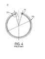
- FIG. 4 A top view of snap ring 77 is shown in FIG. 4 .
- the outer diameter 77G of the snap ring is 1.3 inches
- the ceramic ring 78 FIG. 2
- the snap ring includes dual cavities 77F, which are carved out of the ring's surface, for compressing the ring with the help of pliers.
- snap ring 77 fits into the recess formed by the chamfer of metalized surface 88.
- snap ring 77 at surface 77A, conductively engages metalized surface 88.
- the snap ring conductively engages the upper surface 42 of MCP 16.
- the snap ring also secures and locks down the MCP into a fixed position within the housing.
- an image intensifier tube including a multichannel plate (MCP) having conductive input and output surfaces disposed in a housing.
- MCP multichannel plate
- a conductive lower support is in electrical contact with the output surface of the MCP, and a conductive upper support is disposed above the input surface of the MCP.
- a shape memory alloy (SMA) lockdown is disposed between the input surface of the MCP and the upper support. The SMA lockdown is configured to provide a lockdown for the MCP in the housing.
- MCP multichannel plate
- SMA shape memory alloy
- the SMA lockdown includes an SMA upper surface and an SMA lower surface.
- the SMA upper surface is configured to provide an axial force against the upper support, and the SMA lower surface is in contact with the input surface of the MCP.
- the SMA upper surface may include a chamfer at a peripheral portion of the SMA lockdown, so that the chamfer provides the axial force against the upper support.
- the SMA lockdown includes a memorized state and a deformed state, where the SMA lockdown has a larger diameter in the memorized state than in the deformed state.
- the SMA is configured to provide the axial force against the upper support in the memorized state.
- the SMA is configured free-of the axial force against the upper support in the deformed state.
- the SMA upper surface, the upper support and the input surface of the MCP are in electrical contact with each other.
- the SMA upper surface may be circular including a diameter of D 1
- the SMA lower surface may be circular including a larger diameter of D 2
- the upper support may be circular including an inner aperture. The diameter D 2 is then smaller than the inner aperture for inserting the SMA lockdown through the inner aperture and disposing the SMA lower surface on top of the MCP.
- the present invention includes an image intensifier tube having a lower support and an upper support in a housing.
- a multichannel plate (MCP) is disposed on top of the lower support;
- a shape memory alloy (SMA) element is disposed on top of the MCP; and the upper support is disposed above the SMA element.
- the SMA element is configured for locking down the MCP between the lower support and the upper support.
- the SMA element includes a deformed state and a memorized state.
- the SMA element is configured for locking down the MCP in the memorized state, and configured for insertion between the MCP and the upper support in the deformed state.
- the SMA element has a larger diameter in the memorized state than it does in the deformed state.
- the SMA element, the MCP and the upper support are in electrical contact with each other in the memorized state.
- the SMA element includes a peripheral portion facing another portion of the upper support, and the peripheral portion of the SMA element is configured to provide an axial force against the other portion of the upper support in the memorized state.
- the SMA element includes an SMA upper surface and an SMA lower surface.
- the SMA upper surface is circular including a diameter of D 1 ;
- the SMA lower surface is circular including a larger diameter of D 2 ;
- the upper support is circular including an inner aperture.
- the diameter D 2 is smaller than the inner aperture for inserting the SMA element through the inner aperture and disposing the SMA lower surface on top of the MCP.
- the diameters D 1 and D 2 are of a first relative size in the deformed state for disposing the SMA element on top of the MCP.
- the diameters D 1 and D 2 are of a second relative size in the memorized state for locking down the MCP.
- the first relative size is smaller than the second relative size.
- an image intensifier tube in still another embodiment, includes a lower support and an upper support in a housing, and a shape memory alloy (SMA) element disposed on top of the lower support.
- SMA shape memory alloy
- a multichannel plate (MCP) is disposed on top of the SMA element, and the upper support is disposed above the MCP.
- the SMA element is configured for locking down the MCP between the lower support and the upper support.
- the SMA element includes a deformed state and a memorized state.
- the SMA element is configured for locking down the MCP in the memorized state, and is configured for insertion on top of the lower support in the deformed state.
- the SMA element includes a larger diameter in the memorized state than in the deformed state.
- the SMA element, the MCP and the lower support are in electrical contact with each other in the memorized state.
- the SMA element includes a peripheral portion facing another portion of the lower support, and the peripheral portion of the SMA element is configured to provide an axial force against the other portion of the lower support in the memorized state.
- the SMA element includes an SMA upper surface and an SMA lower surface.
- the SMA upper surface is circular including a diameter of D 1 ;
- the SMA lower surface is circular including a larger diameter of D2; and
- the upper support is circular including an inner aperture.
- the diameter D 2 is smaller than the inner aperture for inserting the SMA element through the inner aperture and disposing the SMA lower surface on top of the lower support.
- the Gen 2 and 3 image intensifier (I 2 ) tubes contain microchannel plates (MCPs) for electron amplification.
- MCP microchannel plates
- the MCP is a thin glass disk, and must be held in place in the I 2 tube securely and in precise location.
- the MCP is placed on an annular ledge called the lower support, and is fixed in place with a locking element.
- Current MCP fixing methods use a tab lockdown, or a snap ring lockdown. The snap ring was described earlier by reference to FIGS. 1-4 .
- the tab lockdown includes a wavy washer, or equivalent, which is placed over the rim of the MCP. Next, a notched annular plate is placed over the wavy washer. The notches of the annular plate pass over tabs in the MCP upper support, and press against the wavy washer to preload it. With the plate in position, the upper support tabs are bent over, thereby, securing both the annular plate and wavy washer against the MCP.
- the snap ring lockdown includes a specially made snap ring ( FIG. 4 ).
- the specially made snap ring with a beveled edge is compressed with pliers and inserted through the upper support and released. As the pliers are released, the snap ring expands, and the beveled edge of the snap ring and the upper support engage each other. The beveled edge translates the radial expansion force of the snap ring into an axial thrust force against the MCP.
- an image intensifier is subject to considerable shock and vibration.
- the MCP must be held very rigidly to prevent deformation.
- Modern gated power supplies also create high frequency voltage pulses that may cause the MCP to flex due to coulombic attraction. If the MCP is not secured all around its circumference, an audible tone may be produced.
- the MCP also has an extremely thin ion barrier film on its exposed face that may be damaged by the slightest touch.
- the tabbed lockdown requires two elements to be placed over the MCP, each with a chance of contacting the ion barrier film over the active area of the MCP. This contact may cause film damage that cannot be detected until the tube is sealed and operating.
- the tab bending operation is an additional opportunity for MCP damage, if the tool slips.
- the wavy washer may not adequately spread the lockdown force around the MCP.
- the unsupported areas may be free to flex, creating audibility and shock problems.
- the need to compress the wavy washer by hand, while bending the tabs, also limits the amount of axial thrust that the tab lockdown method may produce, resulting in reduced MCP rigidity.
- the inventors also discovered that while the snap ring lockdown may overcome some of the problems of the tab lockdown, the snap ring lockdown has produced a few new problems.
- the snap ring provides an even force distribution, but occasionally binds, resulting in a portion of the MCP being left unsupported.
- the snap ring must be compressed with pliers during insertion, but insufficient dexterity or visibility results in hitting the MCP active area.
- the MCP may also crack under the lugs of the snap ring.
- the snap ring has a complicated shape, and is difficult and expensive to manufacture.
- the present invention provides a new locking element, or pressure element for MCP lockdown in the image intensifier housing.
- the new locking element eliminates problems associated with the tab lockdown element and the snap ring lockdown element.
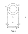
- SMA lockdown 93 includes a lower surface 93C and an opposing upper surface 93A.
- the upper surface has a circular shape of diameter D 1 ; and the lower surface has a circular shape with a larger diameter D 2 .
- An end portion of lower surface 93C extends upwardly a first distance (not labeled) and then bends inwardly to meet the end portion of upper surface 93A. In this manner, chamfer 93B is formed.
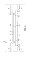
- the exemplary SMA lockdown 93 may be inserted in an image intensifier (I 2 ) housing, designated as 90, and placed on top of MCP 94, as shown in FIG. 5 . This may be accomplished without any force.
- MCP 94 may be placed on top of lower support 92 (shown as an example).
- SMA lockdown 93 may be placed on top of MCP 94. Since the SMA lockdown, in its deformed state (as explained below), has a reduced diameter (D 1 and D 2 ), as compared to snap ring 77 ( FIGS. 3 and 4 ), the SMA lockdown may easily be placed on top of MCP 94 after being inserted through the aperture of upper support 91.
- the SMA lockdown 93 in its deformed state (or pre-use state), has a smaller diameter (shown in cross-section as top surface 93A terminating in chamfer 93B) than a diameter of the same SMA lockdown 93 in its memorized state (or normal-use state) (shown in cross-section as top surface 93A terminating in chamfer 93B').
- SMA lockdown 93 expands to provide a clamping force against the MCP and an axial force against upper support 91.
- the SMA lockdown 93 provides a lock down mechanism for the MCP and fixes the MCP in place.
- the shaped memory element requires no force to install.
- the SMA lockdown element is shaped so that it is easily emplaced, and readily adaptable for automatic insertion. Only after insertion, and only after being heated, does the SMA lockdown element change shape to provide a clamping force to the MCP.
- the shaped memory ring may be continuous without any gap that may lead to cesium migration problems.
- the reduced diameter needed to clear the upper support may be produced by deformation of the SMA lockdown, which may then be recovered to its larger memorized state after being heated.
- the SMA lockdown element is continuous and radially symmetric, it may be fabricated at low cost by stamping, or lathe turning without secondary machining.
- the SMA lockdown 93 is fabricated from shape memory alloys. These alloys may include nickel-titanium-based alloys, which attempt to return to a preset shape when heated. If the shape recovery is hindered, considerable stress is developed within the alloy.
- Shape memory alloys have a heat-treated set memory shape. After heat treatment, the element is generally soft and easily deformed, and stays in a deformed shape, or deformed state. If the deformed element is then heated above a recovery temperature, the SMA element changes crystal structure, and attempts to return to the original shape set during heat treatment, or its memorized state. If the recovery is constrained, the SMA element exerts a force on the constraint that is dependent on the geometry of the element, the temperature and the amount of deformation that the element has endured.
- a shape memory alloy is an alloy that "remembers" its original, cold, forged shape, and which returns to that shape after being deformed by applying heat.
- SMAs may include Ag-Cd alloys, Cu-Al-Ni alloys, Cu-Sn alloys, Cu-Zn alloys, Cu-Zn-Si alloys, Cu-Zn-Al alloys, In-Ti alloys, Ni-Al alloys, Fe-Pt alloys, Mn-Cu alloys, Fe-Mn-Si alloys, and the like.
- Ni-Ti alloys also known as Nitinol
- Ni-Ti alloys are considered a good SMA element.
- these SMA elements may be plastically deformed at a predefined temperature, and upon exposure to thermal manipulation, return to a preset memorized state.
- Some SMA alloys are considered to be one-way shaped memory alloys, and other SMA alloys are considered to be two-way shaped memory alloys.
- a one-way shaped memory alloy when in its cold state, the alloy can be bent or stretched and will hold those shapes until heated above the transition temperature. Upon heating, the shape changes to its original memorized shape. When the alloy cools again, it remains in the memorized shape, until deliberately deformed again.
- the alloy remembers two different shapes: one at low temperature and another at high temperature.
- a one-way shaped memory alloy is likely preferable over the two-way shaped memory alloy.
- the alloy may thus be fabricated into a memorized state (such as the larger diameter of SMA lockdown 93 shown in FIG. 5 ). After heat treatment, the SMA lockdown is generally soft and may be easily deformed, and will stay in its deformed state (such as the smaller diameter of SMA lockdown 93 also shown in FIG. 5 ).
- the SMA lockdown 93 If the deformed SMA lockdown 93 is heated above the recovery temperature, the SMA lockdown changes crystal structure and returns to its original, memorized shape. The larger diameter of the SMA lockdown then stays in its memorized state and effectively provides a lock down for the MCP in its I 2 housing.
- FIG. 6 showed one example of an SMA lockdown.
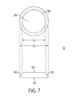
- FIG. 7 shows another example.
- SMA lockdown 96 includes upper surface 96A and lower surface 96C, which are joined by a tapered surface 96B.
- the upper surface has an inner diameter D 3 and the bottom surface an outer diameter D 4 .
- D 4 which is smaller than the inner diameter (not labeled) of the aperture of upper support 91 ( FIG. 5 )
- SMA lockdown 96 may be easily inserted into housing 90, passed through the aperture of the upper support, and then placed on top of MCP 94. This may be accomplished without any specialized tools, and without any force.
- the tapered surface 96B may be formed so that it is parallel to the inner end portion of upper support 91.
- SMA lockdown 96 After heat treatment, above its recovery temperature, SMA lockdown 96 changes crystal structure and returns to its memorized state, which may be similar to the deformed state shown in FIG. 7 , except that SMA lockdown 96 is now expanded and includes larger diameters D 3 and D 4 , as compared to the diameters of its deformed state.
- the SMA lockdown stays in its memorized state and effectively provides a lock down for the MCP in the I 2 housing.
- SMA lockdown Many other configurations and shapes of an SMA lockdown, of course, are possible and are contemplated within the scope of the present invention.
- the only limitations for the SMA lockdown are that the SMA lockdown have a deformed state that allows easy insertion into the I 2 housing and easy placement on top of the MCP.
- the SMA lockdown requires a surface that provides axial pressure against the upper support, when the SMA lockdown is in its larger memorized state.
- an SMA lockdown includes a replacement element for the present snap ring.
- Such an SMA lockdown includes a shape which fits within the same volume of the present snap ring in the housing; no alteration is required to other I 2 tube components in the housing.
- Such a ring may include a circular cross section with one beveled corner. When deformed into a smaller diameter (either concentrically, or by 3 or more "puckers"), the ring fits easily between the MCP and the upper support. After being heated, the ring expands to fill the space between the MCP and the upper support. The final shape may be round, with a diameter large enough to interact with the upper support and produce an axial thrust force against the upper support.
- the SMA lockdown may include a folded sheet metal which unfolds to contact the upper support. Friction or galling between the SMA lockdown and the upper support may cause the thrust force distribution to be less uniform, but is still likely to be better than the present snap ring.
- the SMA lockdown may be a separate pressure plate consisting of a convoluted washer placed above or below the MCP.
- the washer would be pressed flat prior to insertion, and would recover to the convoluted shape which would apply force to the MCP.
- This embodiment may require a separate part to transmit the thrust force to the body, but this embodiment would have an advantage of distributing pressure more uniformly.
Landscapes
- Image-Pickup Tubes, Image-Amplification Tubes, And Storage Tubes (AREA)
Abstract
Description
- The present invention relates, in general, to image intensifier tubes used in night vision goggle (NVG) devices. More specifically, the present invention relates to a shape memory alloy (SMA) for retaining a microchannel plate (MCP) at a precise location within the housing of the image intensifier tube.
- Image intensifier devices multiply the amount of incident light they receive and provide an increase in light output, which can be supplied either to a camera or directly to the eyes of a viewer. Image intensifiers are constructed for a variety of applications and hence vary in both shape and size. These devices are particularly useful for providing images from dark regions and have both industrial and military applications. For example, image intensifiers are used in night vision goggles for enhancing the night vision of aviators and other military personnel performing covert operations. They are employed in security cameras and in medical instruments to help alleviate conditions such as retinitis pigmentosis (night blindness).
- As known, three major components of image intensifier tubes are the photocathode, phosphor screen (anode), and the MCP disposed between the photocathode and anode. These three components are positioned within an evacuated housing or vacuum envelope, thereby permitting electrons to flow from the photocathode through the MCP and the anode. In order for the image intensifier tube to operate, the photocathode and anode are normally coupled to an electric source, whereby the anode is maintained at a higher positive potential than the photocathode. Similarly, the MCP is biased and operates to increase the density of the electron emission set forth by the photocathode. Furthermore, since the photocathode, MCP and anode are all held at different electrical potentials, all three components are electrically isolated from one anther, when retained within the vacuum housing.
- Referring to
FIG. 1 , there is shown a cross-sectional view of a conventional Gen IIIimage intensifier tube 10 of the type manufactured by ITT Night Vision of Roanoke, Va. The prior art Gen IIIimage intensifier tube 10 includes an evacuatedhousing 12 made from the assemblage of several separate components. Withinhousing 12, positioned arephotocathode 14, microchannel plate (MCP) 16, and an inverting fiberoptic element 18, the latter supportingphosphor screen 20. The construction forvacuum housing 12 forms an air tight envelope betweenphotocathode 14 and fiberoptic element 18. - The
photocathode 14 rests upon aconductive support ring 22 at one end ofvacuum housing 12. The abutment ofphotocathode 14 againstsupport ring 22 creates an air tight seal, thereby closing one end ofvacuum housing 12. - The lower end of
vacuum housing 12 is sealed by the presence of anoutput screen flange 72. Theoutput screen flange 72 is joined to fiberoptic element 18 and forms an air tight envelope, thereby closing the other end ofvacuum housing 12. - Between
support ring 22, andscreen flange 72 are additional elements providing annular spacers and electrical terminals forMCP 16 and fiberoptic element 18. These elements are described in detail inUS 5,994,824 A , which is incorporated herein by reference in its entirety. - Completing the description of
FIG. 1 , anupper MCP terminal 32 extends intovacuum housing 12, where it conductively engages a metal hold downring 36 and acontact ring 38. Thecontact ring 38 engages the conductiveupper surface 42 ofMCP 16, while the hold down ring retains the MCP within the housing. Consequently, an electrical bias may be applied toupper surface 42 ofMCP 16 by applying the electrical bias toupper MCP terminal 32 on the exterior ofvacuum housing 12. Similarly, alower MCP terminal 48 extends intovacuum housing 12 and engages the lowerconductive surface 44 ofMCP 16. As such, the lowerconductive surface 44 ofMCP 16 may be coupled to ground by connecting thelower MCP terminal 48 to a ground potential external ofvacuum housing 12. - Referring next to
FIGS. 2 and3 , two examples are shown of howMCP 16 is fixed into position and sandwiched between an upper electrical terminal contactingupper MCP surface 42 and a lower electrical terminal contactinglower MCP surface 44. InFIG.2 , aceramic ring 78 is positioned below support ring 22 (FIG.1 ), and joined to the support ring during a brazing operation. The brazing operation creates an impervious seal betweensupport ring 22 andceramic ring 78. Theceramic ring 78 is part ofring assembly 86 for retaining the MCP. - The
ring assembly 86 includesceramic ring 78,conductive snap ring 77, MCPceramic ring 46, and MCPlower support terminal 48. Theceramic ring 78 includes a firstmetalized surface 88 in electrical contact withconductive snap ring 77, and a secondmetalized surface 89 for providing electrical contact external to the housing and permit an electric source to be applied. Theconductive snap ring 77 is formed of a metal or a metallic alloy.Snap ring 77 has asurface 77B conductively engaging theupper surface 42 of the MCP, and another surface 77A bonded tosurface 88 ofceramic ring 78. - As illustrated, the conducting
snap ring 77 is positioned betweenceramic ring 78 and the MCPupper surface 42. The MCP rests against and is retained bysnap ring 77 andceramic ring 78. The MCP insulatorceramic ring 46 is positioned below and coupled to metalizedsurface 89 by a brazing ring (not shown) interposed between the two elements. The MCP insulatorceramic ring 46 is brazed to bothmetalized surface 89 and MCPlower support 48. - Thus,
snap ring assembly 86 retains the MCP by using metalized ceramic 78 in combination withmetalized snap ring 77 to provide both the lockdown and electrical contact. This feature eliminates the need for complex metal parts including mechanical rings and tabs used in other image intensifiers to hold the MCP in a fixed position. - In another example, as shown in
FIG. 3 , the MCPlower support 48 is employed to both laterally center and axially supportMCP 16. The lower support structure provides atab portion 48A, which is disposed laterally tosurface 16C of the MCP, to prevent lateral dislocation of the MCP, and at the same time to maintain sufficient distance from the snap ring conductive surface in order to prevent short circuiting the device. Theupper support structure 32, on the other hand, is curved downwardly towardsnap ring 77 at itsend portion 32A. The spring force ofsnap ring 77 is effective in forming a normal force againstend portion 32A, so that the snap ring becomes wedged between the MCP and theupper support structure 32. In this manner, theupper surface 42 of the MCP is provided with an electrical potential by way of both the snap ring and the upper support structure. In addition, the MCP is fixed and locked down into position within the image intensifier tube. - A top view of
snap ring 77 is shown inFIG. 4 . In the example shown, theouter diameter 77G of the snap ring is 1.3 inches, whereas the ceramic ring 78 (FIG. 2 ) has an aperture with an inner diameter of 1.24 inches (for example). As a result, the snap ring includesdual cavities 77F, which are carved out of the ring's surface, for compressing the ring with the help of pliers. After compressing its outer diameter,snap ring 77 fits into the recess formed by the chamfer ofmetalized surface 88. In this manner, snapring 77, at surface 77A, conductively engagesmetalized surface 88. In addition, atsurface 77B, the snap ring conductively engages theupper surface 42 ofMCP 16. The snap ring also secures and locks down the MCP into a fixed position within the housing. - The above described method of securing the MCP with the snap ring results in some drawbacks. One drawback is the extra effort required to compress the snap ring with pliers, and properly release the compression after the snap ring is placed on top of the MCP. Another drawback is the possibility of cracking the MCP, when the compression of the snap ring is unevenly released. The present invention, as will be explained, provides a solution to these drawbacks.
- To meet this and other needs, and in view of its purposes, the present invention provides an image intensifier tube including a multichannel plate (MCP) having conductive input and output surfaces disposed in a housing. A conductive lower support is in electrical contact with the output surface of the MCP, and a conductive upper support is disposed above the input surface of the MCP. A shape memory alloy (SMA) lockdown is disposed between the input surface of the MCP and the upper support. The SMA lockdown is configured to provide a lockdown for the MCP in the housing.
- The SMA lockdown includes an SMA upper surface and an SMA lower surface. The SMA upper surface is configured to provide an axial force against the upper support, and the SMA lower surface is in contact with the input surface of the MCP.
- The SMA upper surface may include a chamfer at a peripheral portion of the SMA lockdown, so that the chamfer provides the axial force against the upper support.
- The SMA lockdown includes a memorized state and a deformed state, where the SMA lockdown has a larger diameter in the memorized state than in the deformed state. The SMA is configured to provide the axial force against the upper support in the memorized state. On the other hand, the SMA is configured free-of the axial force against the upper support in the deformed state.
- The SMA upper surface, the upper support and the input surface of the MCP are in electrical contact with each other.
- The SMA upper surface may be circular including a diameter of D1, and the SMA lower surface may be circular including a larger diameter of D2. The upper support may be circular including an inner aperture. The diameter D2 is then smaller than the inner aperture for inserting the SMA lockdown through the inner aperture and disposing the SMA lower surface on top of the MCP.
- In another embodiment, the present invention includes an image intensifier tube having a lower support and an upper support in a housing. A multichannel plate (MCP) is disposed on top of the lower support; a shape memory alloy (SMA) element is disposed on top of the MCP; and the upper support is disposed above the SMA element. The SMA element is configured for locking down the MCP between the lower support and the upper support.
- The SMA element includes a deformed state and a memorized state. The SMA element is configured for locking down the MCP in the memorized state, and configured for insertion between the MCP and the upper support in the deformed state.
- The SMA element has a larger diameter in the memorized state than it does in the deformed state. The SMA element, the MCP and the upper support are in electrical contact with each other in the memorized state. The SMA element includes a peripheral portion facing another portion of the upper support, and the peripheral portion of the SMA element is configured to provide an axial force against the other portion of the upper support in the memorized state.
- The SMA element includes an SMA upper surface and an SMA lower surface. The SMA upper surface is circular including a diameter of D1; the SMA lower surface is circular including a larger diameter of D2; and the upper support is circular including an inner aperture. The diameter D2 is smaller than the inner aperture for inserting the SMA element through the inner aperture and disposing the SMA lower surface on top of the MCP. The diameters D1 and D2 are of a first relative size in the deformed state for disposing the SMA element on top of the MCP. Furthermore, the diameters D1 and D2 are of a second relative size in the memorized state for locking down the MCP. The first relative size is smaller than the second relative size.
- In still another embodiment of the present invention an image intensifier tube includes a lower support and an upper support in a housing, and a shape memory alloy (SMA) element disposed on top of the lower support. A multichannel plate (MCP) is disposed on top of the SMA element, and the upper support is disposed above the MCP. The SMA element is configured for locking down the MCP between the lower support and the upper support.
- The SMA element includes a deformed state and a memorized state. The SMA element is configured for locking down the MCP in the memorized state, and is configured for insertion on top of the lower support in the deformed state. The SMA element includes a larger diameter in the memorized state than in the deformed state. The SMA element, the MCP and the lower support are in electrical contact with each other in the memorized state. The SMA element includes a peripheral portion facing another portion of the lower support, and the peripheral portion of the SMA element is configured to provide an axial force against the other portion of the lower support in the memorized state.
- The SMA element includes an SMA upper surface and an SMA lower surface. The SMA upper surface is circular including a diameter of D1; the SMA lower surface is circular including a larger diameter of D2; and the upper support is circular including an inner aperture. The diameter D2 is smaller than the inner aperture for inserting the SMA element through the inner aperture and disposing the SMA lower surface on top of the lower support.
- It is understood that the foregoing general description and the following detailed description are exemplary, but are not restrictive, of the invention.
- The invention may be understood from the following detailed description when read in connection with the accompanying figures:
-
FIG. 1 is a cross-sectional view of a conventional image intensifier tube. -
FIG. 2 is a cross-sectional view of a conventional snap ring assembly inserted in the image intensifier tube ofFIG. 1 . -
FIG. 3 is cross-sectional view of another conventional snap ring assembly inserted in the image intensifier tube ofFIG. 1 . -
FIG. 4 is a top view of a conventional snap ring used in the image intensifier tube ofFIG. 1 . -
FIG. 5 is an example of a shape memory alloy (SMA) lockdown disposed between an upper support and a lower support of an image intensifier tube, in accordance with an embodiment of the present invention. -
FIG. 6 are top and front views of the exemplary SMA lockdown shown inFIG. 5 , in accordance with an embodiment of the present invention. -
FIG. 7 is another embodiment of an SMA lockdown for insertion into the housing of an image intensifier tube, in accordance with an embodiment of the present invention. - The Gen 2 and 3 image intensifier (I2) tubes contain microchannel plates (MCPs) for electron amplification. The MCP is a thin glass disk, and must be held in place in the I2 tube securely and in precise location. Typically, the MCP is placed on an annular ledge called the lower support, and is fixed in place with a locking element. Current MCP fixing methods use a tab lockdown, or a snap ring lockdown. The snap ring was described earlier by reference to
FIGS. 1-4 . - The tab lockdown will now be briefly described. The tab lockdown includes a wavy washer, or equivalent, which is placed over the rim of the MCP. Next, a notched annular plate is placed over the wavy washer. The notches of the annular plate pass over tabs in the MCP upper support, and press against the wavy washer to preload it. With the plate in position, the upper support tabs are bent over, thereby, securing both the annular plate and wavy washer against the MCP.
- The snap ring lockdown, as previously described, includes a specially made snap ring (
FIG. 4 ). After MCP insertion into the housing, the specially made snap ring with a beveled edge is compressed with pliers and inserted through the upper support and released. As the pliers are released, the snap ring expands, and the beveled edge of the snap ring and the upper support engage each other. The beveled edge translates the radial expansion force of the snap ring into an axial thrust force against the MCP. - The inventors discovered that both, the tab lockdown and the snap ring lockdown, have notable drawbacks. During operation, an image intensifier is subject to considerable shock and vibration. In addition, the MCP must be held very rigidly to prevent deformation. Modern gated power supplies also create high frequency voltage pulses that may cause the MCP to flex due to coulombic attraction. If the MCP is not secured all around its circumference, an audible tone may be produced. The MCP also has an extremely thin ion barrier film on its exposed face that may be damaged by the slightest touch.
- The tabbed lockdown requires two elements to be placed over the MCP, each with a chance of contacting the ion barrier film over the active area of the MCP. This contact may cause film damage that cannot be detected until the tube is sealed and operating.
- Furthermore, the tab bending operation is an additional opportunity for MCP damage, if the tool slips. Furthermore, the wavy washer may not adequately spread the lockdown force around the MCP. The unsupported areas may be free to flex, creating audibility and shock problems. The need to compress the wavy washer by hand, while bending the tabs, also limits the amount of axial thrust that the tab lockdown method may produce, resulting in reduced MCP rigidity.
- The inventors also discovered that while the snap ring lockdown may overcome some of the problems of the tab lockdown, the snap ring lockdown has produced a few new problems. The snap ring provides an even force distribution, but occasionally binds, resulting in a portion of the MCP being left unsupported. The snap ring must be compressed with pliers during insertion, but insufficient dexterity or visibility results in hitting the MCP active area. The MCP may also crack under the lugs of the snap ring. In addition, the snap ring has a complicated shape, and is difficult and expensive to manufacture.
- The present invention provides a new locking element, or pressure element for MCP lockdown in the image intensifier housing. As will now be explained, the new locking element eliminates problems associated with the tab lockdown element and the snap ring lockdown element.
- Referring now to
FIGS. 5 and6 , there is shown an example of an element for MCP lockdown fabricated from shape memory alloys (SMAs). In the example shown inFIG. 6 ,SMA lockdown 93 includes alower surface 93C and an opposingupper surface 93A. The upper surface has a circular shape of diameter D1; and the lower surface has a circular shape with a larger diameter D2. An end portion oflower surface 93C extends upwardly a first distance (not labeled) and then bends inwardly to meet the end portion ofupper surface 93A. In this manner,chamfer 93B is formed. - The
exemplary SMA lockdown 93 may be inserted in an image intensifier (I2) housing, designated as 90, and placed on top ofMCP 94, as shown inFIG. 5 . This may be accomplished without any force. During assembly,MCP 94 may be placed on top of lower support 92 (shown as an example). Next,SMA lockdown 93 may be placed on top ofMCP 94. Since the SMA lockdown, in its deformed state (as explained below), has a reduced diameter (D1 and D2), as compared to snap ring 77 (FIGS. 3 and4 ), the SMA lockdown may easily be placed on top ofMCP 94 after being inserted through the aperture ofupper support 91. - In the example shown in
FIG. 5 , in its deformed state (or pre-use state), theSMA lockdown 93 has a smaller diameter (shown in cross-section astop surface 93A terminating inchamfer 93B) than a diameter of thesame SMA lockdown 93 in its memorized state (or normal-use state) (shown in cross-section astop surface 93A terminating inchamfer 93B'). In its memorized state, after being heated,SMA lockdown 93 expands to provide a clamping force against the MCP and an axial force againstupper support 91. In this manner, after transitioning into its memorized state, theSMA lockdown 93 provides a lock down mechanism for the MCP and fixes the MCP in place. - As described above, the shaped memory element requires no force to install. The SMA lockdown element is shaped so that it is easily emplaced, and readily adaptable for automatic insertion. Only after insertion, and only after being heated, does the SMA lockdown element change shape to provide a clamping force to the MCP.
- Unlike the snap ring lockdown which has gaps in its structure, the shaped memory ring may be continuous without any gap that may lead to cesium migration problems. The reduced diameter needed to clear the upper support may be produced by deformation of the SMA lockdown, which may then be recovered to its larger memorized state after being heated.
- Because the SMA lockdown element is continuous and radially symmetric, it may be fabricated at low cost by stamping, or lathe turning without secondary machining.
- The
SMA lockdown 93 is fabricated from shape memory alloys. These alloys may include nickel-titanium-based alloys, which attempt to return to a preset shape when heated. If the shape recovery is hindered, considerable stress is developed within the alloy. - Shape memory alloys have a heat-treated set memory shape. After heat treatment, the element is generally soft and easily deformed, and stays in a deformed shape, or deformed state. If the deformed element is then heated above a recovery temperature, the SMA element changes crystal structure, and attempts to return to the original shape set during heat treatment, or its memorized state. If the recovery is constrained, the SMA element exerts a force on the constraint that is dependent on the geometry of the element, the temperature and the amount of deformation that the element has endured.
- In general, a shape memory alloy (SMA) is an alloy that "remembers" its original, cold, forged shape, and which returns to that shape after being deformed by applying heat. In addition to nickel-titanium (Ni-Ti) alloys, SMAs may include Ag-Cd alloys, Cu-Al-Ni alloys, Cu-Sn alloys, Cu-Zn alloys, Cu-Zn-Si alloys, Cu-Zn-Al alloys, In-Ti alloys, Ni-Al alloys, Fe-Pt alloys, Mn-Cu alloys, Fe-Mn-Si alloys, and the like. Currently, Ni-Ti alloys (also known as Nitinol) are considered a good SMA element. Generally, these SMA elements may be plastically deformed at a predefined temperature, and upon exposure to thermal manipulation, return to a preset memorized state. Some SMA alloys are considered to be one-way shaped memory alloys, and other SMA alloys are considered to be two-way shaped memory alloys.
- In a one-way shaped memory alloy, when in its cold state, the alloy can be bent or stretched and will hold those shapes until heated above the transition temperature. Upon heating, the shape changes to its original memorized shape. When the alloy cools again, it remains in the memorized shape, until deliberately deformed again. In a two-way shaped memory alloy, the alloy remembers two different shapes: one at low temperature and another at high temperature.
- In the present invention, a one-way shaped memory alloy is likely preferable over the two-way shaped memory alloy. The alloy may thus be fabricated into a memorized state (such as the larger diameter of
SMA lockdown 93 shown inFIG. 5 ). After heat treatment, the SMA lockdown is generally soft and may be easily deformed, and will stay in its deformed state (such as the smaller diameter ofSMA lockdown 93 also shown inFIG. 5 ). - If the
deformed SMA lockdown 93 is heated above the recovery temperature, the SMA lockdown changes crystal structure and returns to its original, memorized shape. The larger diameter of the SMA lockdown then stays in its memorized state and effectively provides a lock down for the MCP in its I2 housing. -
FIG. 6 showed one example of an SMA lockdown.FIG. 7 shows another example. As shown,SMA lockdown 96 includesupper surface 96A andlower surface 96C, which are joined by atapered surface 96B. The upper surface has an inner diameter D3 and the bottom surface an outer diameter D4. As long as the deformed state shown inFIG. 7 has an outer diameter D4 which is smaller than the inner diameter (not labeled) of the aperture of upper support 91 (FIG. 5 ),SMA lockdown 96 may be easily inserted intohousing 90, passed through the aperture of the upper support, and then placed on top ofMCP 94. This may be accomplished without any specialized tools, and without any force. Thetapered surface 96B may be formed so that it is parallel to the inner end portion ofupper support 91. - After heat treatment, above its recovery temperature,
SMA lockdown 96 changes crystal structure and returns to its memorized state, which may be similar to the deformed state shown inFIG. 7 , except thatSMA lockdown 96 is now expanded and includes larger diameters D3 and D4, as compared to the diameters of its deformed state. The SMA lockdown stays in its memorized state and effectively provides a lock down for the MCP in the I2 housing. - Many other configurations and shapes of an SMA lockdown, of course, are possible and are contemplated within the scope of the present invention. The only limitations for the SMA lockdown are that the SMA lockdown have a deformed state that allows easy insertion into the I2 housing and easy placement on top of the MCP. In addition, the SMA lockdown requires a surface that provides axial pressure against the upper support, when the SMA lockdown is in its larger memorized state.
- One possible configuration for an SMA lockdown includes a replacement element for the present snap ring. Such an SMA lockdown includes a shape which fits within the same volume of the present snap ring in the housing; no alteration is required to other I2 tube components in the housing. Such a ring may include a circular cross section with one beveled corner. When deformed into a smaller diameter (either concentrically, or by 3 or more "puckers"), the ring fits easily between the MCP and the upper support. After being heated, the ring expands to fill the space between the MCP and the upper support. The final shape may be round, with a diameter large enough to interact with the upper support and produce an axial thrust force against the upper support.
- In another embodiment, the SMA lockdown may include a folded sheet metal which unfolds to contact the upper support. Friction or galling between the SMA lockdown and the upper support may cause the thrust force distribution to be less uniform, but is still likely to be better than the present snap ring.
- In yet another embodiment, the SMA lockdown may be a separate pressure plate consisting of a convoluted washer placed above or below the MCP. The washer would be pressed flat prior to insertion, and would recover to the convoluted shape which would apply force to the MCP. This embodiment may require a separate part to transmit the thrust force to the body, but this embodiment would have an advantage of distributing pressure more uniformly.
- Although the invention is illustrated and described herein with reference to the claims and specific embodiments, the invention is not intended to be limited to the details shown. Rather, various modifications may be made in the details within the scope and range of equivalents of the claims and without departing from the invention.
Claims (15)
- An image intensifier tube comprising:a microchannel plate (MCP) (94) having conductive input and output surfaces disposed in a housing,a conductive lower support (92) in electrical contact with the output surface of the MCP,a conductive upper support (91) disposed above the input surface of the MCP, anda shape memory alloy (SMA) lockdown (93, 96) disposed between the input surface of the MCP and the upper support,wherein the SMA lockdown is configured to provide a lockdown for the MCP in the housing.
- The image intensifier tube of claim 1, wherein
the SMA lockdown includes an SMA upper surface (93A, 96A) and an SMA lower surface (93C, 96C),
the SMA upper surface is configured to provide an axial force against the upper support, and
the SMA lower surface is in contact with the input surface of the MCP. - The image intensifier tube of claim 2, wherein
the SMA upper surface includes a chamfer (93B) at a peripheral portion of the SMA lockdown, and
the chamfer provides the axial force against the upper support. - The image intensifier tube of claim 2 or 3, wherein
the SMA lockdown includes a memorized state and a deformed state, the SMA lockdown having a larger diameter in the memorized state than in the deformed state, and- the SMA upper surface provides the axial force against the upper support in the memorized state; and/or- the SMA upper surface is configured free-of the axial force against the upper support in the deformed state. - The image intensifier tube of one of claims 2 to 4, wherein
the SMA upper surface, the upper support and the input surface of the MCP are in electrical contact with each other. - The image intensifier tube of one of claims 2 to 5, wherein
the SMA upper surface is circular including a diameter of D1,
the SMA lower surface is circular including a larger diameter of D2,
the upper support is circular including an inner aperture, and
the diameter D2 is smaller than the inner aperture for inserting the SMA lockdown through the inner aperture and disposing the SMA lower surface on top of the MCP. - The image intensifier tube of one of the preceding claims, wherein:the shape memory alloy (SMA) is disposed on top of the MCP,the upper support is disposed above the SMA, andthe SMA is configured for locking down the MCP between the lower support and the upper support.
- The image intensifier tube of one of the preceding claims, wherein
the SMA includes a deformed state and a memorized state,
the SMA is configured for locking down the MCP in the memorized state, and the SMA is configured for insertion between the MCP and the upper support in the deformed state. - The image intensifier tube of one of claims 4 to 8, wherein
the SMA includes a larger diameter in the memorized state than in the deformed state. - The image intensifier tube of one of claims 4 to 9, wherein
the SMA, the MCP and the upper support are in electrical contact with each other in the memorized state. - The image intensifier tube of one of claims 4 to 10, wherein
the SMA includes a peripheral portion facing another portion of the upper support, and
the peripheral portion of the SMA is configured to provide an axial force against the other portion of the upper support in the memorized state. - The image intensifier tube of one of the preceding claims, wherein
the SMA includes an SMA upper surface and an SMA lower surface,
the SMA upper surface is circular including a diameter of D1,
the SMA lower surface is circular including a larger diameter of D2,
the upper support is circular including an inner aperture, and
the diameter D2 is smaller than the inner aperture for inserting the SMA through the inner aperture and disposing the SMA lower surface on top of the MCP. - The image intensifier tube of claim 12 wherein
the diameters D1 and D2 are of a first relative size in the deformed state for disposing the SMA on top of the MCP,
the diameters D1 and D2 are of a second relative size in the memorized state for locking down the MCP, and
the first relative size is smaller than the second relative size. - The image intensifier tube of one of claims 4 to 13, wherein
the SMA, the MCP and the lower support are in electrical contact with each other in the memorized state. - The image intensifier tube of one of claims 4 to 14, wherein
the SMA includes a peripheral portion facing another portion of the lower support, and
the peripheral portion of the SMA is configured to provide an axial force against the other portion of the lower support in the memorized state.
Applications Claiming Priority (1)
| Application Number | Priority Date | Filing Date | Title |
|---|---|---|---|
| US12/767,121 US8076627B2 (en) | 2010-04-26 | 2010-04-26 | Shape memory alloy for MCP lockdown |
Publications (4)
| Publication Number | Publication Date |
|---|---|
| EP2387061A2 true EP2387061A2 (en) | 2011-11-16 |
| EP2387061A8 EP2387061A8 (en) | 2012-03-07 |
| EP2387061A3 EP2387061A3 (en) | 2013-02-13 |
| EP2387061B1 EP2387061B1 (en) | 2015-12-02 |
Family
ID=44678123
Family Applications (1)
| Application Number | Title | Priority Date | Filing Date |
|---|---|---|---|
| EP11162195.9A Not-in-force EP2387061B1 (en) | 2010-04-26 | 2011-04-13 | Shape memory alloy for MCP lockdown |
Country Status (3)
| Country | Link |
|---|---|
| US (1) | US8076627B2 (en) |
| EP (1) | EP2387061B1 (en) |
| JP (1) | JP5805988B2 (en) |
Families Citing this family (4)
| Publication number | Priority date | Publication date | Assignee | Title |
|---|---|---|---|---|
| US9734977B2 (en) * | 2015-07-16 | 2017-08-15 | Intevac, Inc. | Image intensifier with indexed compliant anode assembly |
| DE102015121818A1 (en) * | 2015-12-15 | 2017-06-22 | Biotronik Se & Co. Kg | Implementation of a medical electronic device, method for producing such and medical electronic device |
| US10121817B2 (en) * | 2015-12-17 | 2018-11-06 | General Electric Company | Radiation detector for use as an image intensifier |
| CN119065065B (en) * | 2023-05-30 | 2025-10-21 | 中国科学院西安光学精密机械研究所 | A high-precision optical fiber microhole precision coupling device and method |
Citations (1)
| Publication number | Priority date | Publication date | Assignee | Title |
|---|---|---|---|---|
| US5994824A (en) | 1997-07-24 | 1999-11-30 | Itt Manufacturing Enterprises | Light weight/small image intensifier tube |
Family Cites Families (9)
| Publication number | Priority date | Publication date | Assignee | Title |
|---|---|---|---|---|
| JPS6053277A (en) * | 1983-08-30 | 1985-03-26 | Yaskawa Electric Mfg Co Ltd | Sealing method of pressure container safety device |
| JPS6070649A (en) * | 1983-09-26 | 1985-04-22 | Nec Corp | Image tube |
| JPS6195731A (en) * | 1984-10-15 | 1986-05-14 | Fuji Valve Kk | Manufacture of axis with stop ring |
| JPS62131453A (en) * | 1985-12-03 | 1987-06-13 | Hamamatsu Photonics Kk | Image tube |
| US4675472A (en) * | 1986-08-04 | 1987-06-23 | Beta Phase, Inc. | Integrated circuit package and seal therefor |
| DE69331239T2 (en) * | 1993-09-29 | 2002-10-17 | Itt Manufacturing Enterprises, Inc. | VACUUM CHAMBER FOR AN IMAGE AMPLIFIER TUBE |
| JP2588412Y2 (en) * | 1993-12-17 | 1999-01-13 | 東芝硝子株式会社 | Substrate fixing device |
| US20060145016A1 (en) * | 2004-12-30 | 2006-07-06 | The Boeing Company | Mating of spacecraft components using shape memory materials |
| CA2621300A1 (en) * | 2008-02-14 | 2009-08-14 | Schlumberger Canada Limited | Shape memory hermetic seal and threaded joint incorporating same |
-
2010
- 2010-04-26 US US12/767,121 patent/US8076627B2/en active Active
-
2011
- 2011-04-13 EP EP11162195.9A patent/EP2387061B1/en not_active Not-in-force
- 2011-04-25 JP JP2011097493A patent/JP5805988B2/en active Active
Patent Citations (1)
| Publication number | Priority date | Publication date | Assignee | Title |
|---|---|---|---|---|
| US5994824A (en) | 1997-07-24 | 1999-11-30 | Itt Manufacturing Enterprises | Light weight/small image intensifier tube |
Also Published As
| Publication number | Publication date |
|---|---|
| EP2387061B1 (en) | 2015-12-02 |
| US8076627B2 (en) | 2011-12-13 |
| JP5805988B2 (en) | 2015-11-10 |
| US20110260608A1 (en) | 2011-10-27 |
| EP2387061A8 (en) | 2012-03-07 |
| EP2387061A3 (en) | 2013-02-13 |
| JP2011238607A (en) | 2011-11-24 |
Similar Documents
| Publication | Publication Date | Title |
|---|---|---|
| EP2387061B1 (en) | Shape memory alloy for MCP lockdown | |
| US20030127958A1 (en) | Night vision device and method | |
| EP2187424A2 (en) | Apparatus and method for aligning an image sensor | |
| US5994824A (en) | Light weight/small image intensifier tube | |
| US3299328A (en) | Semiconductor device with pressure contact | |
| US20100102209A1 (en) | Apparatus and method for sealing an image intensifier device | |
| US8022606B2 (en) | Electron multipler and electron detector | |
| CN108933072B (en) | Anode and X-ray generating tube, X-ray generating apparatus and radiography system | |
| US7482571B2 (en) | Low cost planar image intensifier tube structure | |
| US5118925A (en) | Electromagnetic interference shielding device for image intensifiers | |
| US6331753B1 (en) | Image intensifier tube | |
| JPH0644929A (en) | Image intensifier | |
| US20100102205A1 (en) | Vented header assembly of an image intensifier device | |
| US6040657A (en) | Thin faceplate image intensifier tube having an improved vacuum housing | |
| WO2000051159A1 (en) | Image intensifier with optimized mcp | |
| US4406973A (en) | Black glass shield and method for absorbing stray light for image intensifiers | |
| US6957992B2 (en) | Image intensification tube | |
| GB1566851A (en) | Image intensifier tube | |
| CN205692797U (en) | A kind of microchannel plate possessing protection device | |
| US3152384A (en) | Method of forming bowl shaped screen for electron discharge tubes | |
| JP6810127B2 (en) | Image intensifier with indexed compliant anode assembly | |
| EP2940346B1 (en) | Shock isolation protection of sensitive components | |
| EP0366500B1 (en) | An image intensifier device | |
| KR102797632B1 (en) | Method for manufacturing a sealed electrical connection provided in a ceramic case and an image intensifier including a ceramic case provided with a sealed electrical connection | |
| US6288839B1 (en) | Replacement assembly for an image intensifier tube utilizing an input relay lens |
Legal Events
| Date | Code | Title | Description |
|---|---|---|---|
| AK | Designated contracting states |
Kind code of ref document: A2 Designated state(s): AL AT BE BG CH CY CZ DE DK EE ES FI FR GB GR HR HU IE IS IT LI LT LU LV MC MK MT NL NO PL PT RO RS SE SI SK SM TR |
|
| AX | Request for extension of the european patent |
Extension state: BA ME |
|
| PUAI | Public reference made under article 153(3) epc to a published international application that has entered the european phase |
Free format text: ORIGINAL CODE: 0009012 |
|
| RIN1 | Information on inventor provided before grant (corrected) |
Inventor name: ROSINE, STEVEN DAVID Inventor name: MILLS, MICHAEL SCOTT Inventor name: NGUYEN, KHANG VINH |
|
| RAP1 | Party data changed (applicant data changed or rights of an application transferred) |
Owner name: EXELIS INC. |
|
| PUAL | Search report despatched |
Free format text: ORIGINAL CODE: 0009013 |
|
| RIC1 | Information provided on ipc code assigned before grant |
Ipc: H01J 31/50 20060101AFI20121219BHEP |
|
| AK | Designated contracting states |
Kind code of ref document: A3 Designated state(s): AL AT BE BG CH CY CZ DE DK EE ES FI FR GB GR HR HU IE IS IT LI LT LU LV MC MK MT NL NO PL PT RO RS SE SI SK SM TR |
|
| AX | Request for extension of the european patent |
Extension state: BA ME |
|
| 17P | Request for examination filed |
Effective date: 20130812 |
|
| RBV | Designated contracting states (corrected) |
Designated state(s): AL AT BE BG CH CY CZ DE DK EE ES FI FR GB GR HR HU IE IS IT LI LT LU LV MC MK MT NL NO PL PT RO RS SE SI SK SM TR |
|
| GRAP | Despatch of communication of intention to grant a patent |
Free format text: ORIGINAL CODE: EPIDOSNIGR1 |
|
| INTG | Intention to grant announced |
Effective date: 20150710 |
|
| GRAS | Grant fee paid |
Free format text: ORIGINAL CODE: EPIDOSNIGR3 |
|
| RAP1 | Party data changed (applicant data changed or rights of an application transferred) |
Owner name: EXELIS INC. |
|
| GRAA | (expected) grant |
Free format text: ORIGINAL CODE: 0009210 |
|
| AK | Designated contracting states |
Kind code of ref document: B1 Designated state(s): AL AT BE BG CH CY CZ DE DK EE ES FI FR GB GR HR HU IE IS IT LI LT LU LV MC MK MT NL NO PL PT RO RS SE SI SK SM TR |
|
| REG | Reference to a national code |
Ref country code: GB Ref legal event code: FG4D |
|
| REG | Reference to a national code |
Ref country code: AT Ref legal event code: REF Ref document number: 763957 Country of ref document: AT Kind code of ref document: T Effective date: 20151215 Ref country code: CH Ref legal event code: EP |
|
| REG | Reference to a national code |
Ref country code: IE Ref legal event code: FG4D |
|
| REG | Reference to a national code |
Ref country code: DE Ref legal event code: R096 Ref document number: 602011021761 Country of ref document: DE |
|
| REG | Reference to a national code |
Ref country code: NL Ref legal event code: FP |
|
| REG | Reference to a national code |
Ref country code: LT Ref legal event code: MG4D |
|
| REG | Reference to a national code |
Ref country code: AT Ref legal event code: MK05 Ref document number: 763957 Country of ref document: AT Kind code of ref document: T Effective date: 20151202 |
|
| REG | Reference to a national code |
Ref country code: FR Ref legal event code: PLFP Year of fee payment: 6 |
|
| PG25 | Lapsed in a contracting state [announced via postgrant information from national office to epo] |
Ref country code: LT Free format text: LAPSE BECAUSE OF FAILURE TO SUBMIT A TRANSLATION OF THE DESCRIPTION OR TO PAY THE FEE WITHIN THE PRESCRIBED TIME-LIMIT Effective date: 20151202 Ref country code: NO Free format text: LAPSE BECAUSE OF FAILURE TO SUBMIT A TRANSLATION OF THE DESCRIPTION OR TO PAY THE FEE WITHIN THE PRESCRIBED TIME-LIMIT Effective date: 20160302 Ref country code: ES Free format text: LAPSE BECAUSE OF FAILURE TO SUBMIT A TRANSLATION OF THE DESCRIPTION OR TO PAY THE FEE WITHIN THE PRESCRIBED TIME-LIMIT Effective date: 20151202 |
|
| PG25 | Lapsed in a contracting state [announced via postgrant information from national office to epo] |
Ref country code: LV Free format text: LAPSE BECAUSE OF FAILURE TO SUBMIT A TRANSLATION OF THE DESCRIPTION OR TO PAY THE FEE WITHIN THE PRESCRIBED TIME-LIMIT Effective date: 20151202 Ref country code: RS Free format text: LAPSE BECAUSE OF FAILURE TO SUBMIT A TRANSLATION OF THE DESCRIPTION OR TO PAY THE FEE WITHIN THE PRESCRIBED TIME-LIMIT Effective date: 20151202 Ref country code: GR Free format text: LAPSE BECAUSE OF FAILURE TO SUBMIT A TRANSLATION OF THE DESCRIPTION OR TO PAY THE FEE WITHIN THE PRESCRIBED TIME-LIMIT Effective date: 20160303 Ref country code: FI Free format text: LAPSE BECAUSE OF FAILURE TO SUBMIT A TRANSLATION OF THE DESCRIPTION OR TO PAY THE FEE WITHIN THE PRESCRIBED TIME-LIMIT Effective date: 20151202 Ref country code: AT Free format text: LAPSE BECAUSE OF FAILURE TO SUBMIT A TRANSLATION OF THE DESCRIPTION OR TO PAY THE FEE WITHIN THE PRESCRIBED TIME-LIMIT Effective date: 20151202 Ref country code: PL Free format text: LAPSE BECAUSE OF FAILURE TO SUBMIT A TRANSLATION OF THE DESCRIPTION OR TO PAY THE FEE WITHIN THE PRESCRIBED TIME-LIMIT Effective date: 20151202 Ref country code: SE Free format text: LAPSE BECAUSE OF FAILURE TO SUBMIT A TRANSLATION OF THE DESCRIPTION OR TO PAY THE FEE WITHIN THE PRESCRIBED TIME-LIMIT Effective date: 20151202 |
|
| PG25 | Lapsed in a contracting state [announced via postgrant information from national office to epo] |
Ref country code: IS Free format text: LAPSE BECAUSE OF FAILURE TO SUBMIT A TRANSLATION OF THE DESCRIPTION OR TO PAY THE FEE WITHIN THE PRESCRIBED TIME-LIMIT Effective date: 20151202 |
|
| PG25 | Lapsed in a contracting state [announced via postgrant information from national office to epo] |
Ref country code: CZ Free format text: LAPSE BECAUSE OF FAILURE TO SUBMIT A TRANSLATION OF THE DESCRIPTION OR TO PAY THE FEE WITHIN THE PRESCRIBED TIME-LIMIT Effective date: 20151202 Ref country code: IT Free format text: LAPSE BECAUSE OF FAILURE TO SUBMIT A TRANSLATION OF THE DESCRIPTION OR TO PAY THE FEE WITHIN THE PRESCRIBED TIME-LIMIT Effective date: 20151202 |
|
| PG25 | Lapsed in a contracting state [announced via postgrant information from national office to epo] |
Ref country code: EE Free format text: LAPSE BECAUSE OF FAILURE TO SUBMIT A TRANSLATION OF THE DESCRIPTION OR TO PAY THE FEE WITHIN THE PRESCRIBED TIME-LIMIT Effective date: 20151202 Ref country code: BE Free format text: LAPSE BECAUSE OF NON-PAYMENT OF DUE FEES Effective date: 20160430 Ref country code: SM Free format text: LAPSE BECAUSE OF FAILURE TO SUBMIT A TRANSLATION OF THE DESCRIPTION OR TO PAY THE FEE WITHIN THE PRESCRIBED TIME-LIMIT Effective date: 20151202 Ref country code: RO Free format text: LAPSE BECAUSE OF FAILURE TO SUBMIT A TRANSLATION OF THE DESCRIPTION OR TO PAY THE FEE WITHIN THE PRESCRIBED TIME-LIMIT Effective date: 20151202 Ref country code: IS Free format text: LAPSE BECAUSE OF FAILURE TO SUBMIT A TRANSLATION OF THE DESCRIPTION OR TO PAY THE FEE WITHIN THE PRESCRIBED TIME-LIMIT Effective date: 20160402 Ref country code: SK Free format text: LAPSE BECAUSE OF FAILURE TO SUBMIT A TRANSLATION OF THE DESCRIPTION OR TO PAY THE FEE WITHIN THE PRESCRIBED TIME-LIMIT Effective date: 20151202 Ref country code: PT Free format text: LAPSE BECAUSE OF FAILURE TO SUBMIT A TRANSLATION OF THE DESCRIPTION OR TO PAY THE FEE WITHIN THE PRESCRIBED TIME-LIMIT Effective date: 20160404 |
|
| REG | Reference to a national code |
Ref country code: DE Ref legal event code: R097 Ref document number: 602011021761 Country of ref document: DE |
|
| PLBE | No opposition filed within time limit |
Free format text: ORIGINAL CODE: 0009261 |
|
| STAA | Information on the status of an ep patent application or granted ep patent |
Free format text: STATUS: NO OPPOSITION FILED WITHIN TIME LIMIT |
|
| PG25 | Lapsed in a contracting state [announced via postgrant information from national office to epo] |
Ref country code: DK Free format text: LAPSE BECAUSE OF FAILURE TO SUBMIT A TRANSLATION OF THE DESCRIPTION OR TO PAY THE FEE WITHIN THE PRESCRIBED TIME-LIMIT Effective date: 20151202 |
|
| REG | Reference to a national code |
Ref country code: DE Ref legal event code: R119 Ref document number: 602011021761 Country of ref document: DE |
|
| 26N | No opposition filed |
Effective date: 20160905 |
|
| PG25 | Lapsed in a contracting state [announced via postgrant information from national office to epo] |
Ref country code: SI Free format text: LAPSE BECAUSE OF FAILURE TO SUBMIT A TRANSLATION OF THE DESCRIPTION OR TO PAY THE FEE WITHIN THE PRESCRIBED TIME-LIMIT Effective date: 20151202 |
|
| REG | Reference to a national code |
Ref country code: CH Ref legal event code: PL |
|
| GBPC | Gb: european patent ceased through non-payment of renewal fee |
Effective date: 20160413 |
|
| PG25 | Lapsed in a contracting state [announced via postgrant information from national office to epo] |
Ref country code: BE Free format text: LAPSE BECAUSE OF FAILURE TO SUBMIT A TRANSLATION OF THE DESCRIPTION OR TO PAY THE FEE WITHIN THE PRESCRIBED TIME-LIMIT Effective date: 20151202 Ref country code: LU Free format text: LAPSE BECAUSE OF FAILURE TO SUBMIT A TRANSLATION OF THE DESCRIPTION OR TO PAY THE FEE WITHIN THE PRESCRIBED TIME-LIMIT Effective date: 20160413 |
|
| REG | Reference to a national code |
Ref country code: IE Ref legal event code: MM4A |
|
| PG25 | Lapsed in a contracting state [announced via postgrant information from national office to epo] |
Ref country code: LI Free format text: LAPSE BECAUSE OF NON-PAYMENT OF DUE FEES Effective date: 20160430 Ref country code: GB Free format text: LAPSE BECAUSE OF NON-PAYMENT OF DUE FEES Effective date: 20160413 Ref country code: CH Free format text: LAPSE BECAUSE OF NON-PAYMENT OF DUE FEES Effective date: 20160430 Ref country code: DE Free format text: LAPSE BECAUSE OF NON-PAYMENT OF DUE FEES Effective date: 20161101 |
|
| REG | Reference to a national code |
Ref country code: FR Ref legal event code: PLFP Year of fee payment: 7 |
|
| PG25 | Lapsed in a contracting state [announced via postgrant information from national office to epo] |
Ref country code: IE Free format text: LAPSE BECAUSE OF NON-PAYMENT OF DUE FEES Effective date: 20160413 |
|
| REG | Reference to a national code |
Ref country code: FR Ref legal event code: PLFP Year of fee payment: 8 |
|
| PG25 | Lapsed in a contracting state [announced via postgrant information from national office to epo] |
Ref country code: CY Free format text: LAPSE BECAUSE OF FAILURE TO SUBMIT A TRANSLATION OF THE DESCRIPTION OR TO PAY THE FEE WITHIN THE PRESCRIBED TIME-LIMIT Effective date: 20151202 Ref country code: HU Free format text: LAPSE BECAUSE OF FAILURE TO SUBMIT A TRANSLATION OF THE DESCRIPTION OR TO PAY THE FEE WITHIN THE PRESCRIBED TIME-LIMIT; INVALID AB INITIO Effective date: 20110413 |
|
| PG25 | Lapsed in a contracting state [announced via postgrant information from national office to epo] |
Ref country code: HR Free format text: LAPSE BECAUSE OF FAILURE TO SUBMIT A TRANSLATION OF THE DESCRIPTION OR TO PAY THE FEE WITHIN THE PRESCRIBED TIME-LIMIT Effective date: 20151202 Ref country code: MK Free format text: LAPSE BECAUSE OF FAILURE TO SUBMIT A TRANSLATION OF THE DESCRIPTION OR TO PAY THE FEE WITHIN THE PRESCRIBED TIME-LIMIT Effective date: 20151202 Ref country code: MT Free format text: LAPSE BECAUSE OF NON-PAYMENT OF DUE FEES Effective date: 20160430 Ref country code: MC Free format text: LAPSE BECAUSE OF FAILURE TO SUBMIT A TRANSLATION OF THE DESCRIPTION OR TO PAY THE FEE WITHIN THE PRESCRIBED TIME-LIMIT Effective date: 20151202 Ref country code: TR Free format text: LAPSE BECAUSE OF FAILURE TO SUBMIT A TRANSLATION OF THE DESCRIPTION OR TO PAY THE FEE WITHIN THE PRESCRIBED TIME-LIMIT Effective date: 20151202 |
|
| PG25 | Lapsed in a contracting state [announced via postgrant information from national office to epo] |
Ref country code: BG Free format text: LAPSE BECAUSE OF FAILURE TO SUBMIT A TRANSLATION OF THE DESCRIPTION OR TO PAY THE FEE WITHIN THE PRESCRIBED TIME-LIMIT Effective date: 20151202 |
|
| PG25 | Lapsed in a contracting state [announced via postgrant information from national office to epo] |
Ref country code: AL Free format text: LAPSE BECAUSE OF FAILURE TO SUBMIT A TRANSLATION OF THE DESCRIPTION OR TO PAY THE FEE WITHIN THE PRESCRIBED TIME-LIMIT Effective date: 20151202 |
|
| PGFP | Annual fee paid to national office [announced via postgrant information from national office to epo] |
Ref country code: NL Payment date: 20220422 Year of fee payment: 12 |
|
| PGFP | Annual fee paid to national office [announced via postgrant information from national office to epo] |
Ref country code: FR Payment date: 20220427 Year of fee payment: 12 |
|
| P01 | Opt-out of the competence of the unified patent court (upc) registered |
Effective date: 20230627 |
|
| REG | Reference to a national code |
Ref country code: NL Ref legal event code: MM Effective date: 20230501 |
|
| PG25 | Lapsed in a contracting state [announced via postgrant information from national office to epo] |
Ref country code: NL Free format text: LAPSE BECAUSE OF NON-PAYMENT OF DUE FEES Effective date: 20230501 Ref country code: FR Free format text: LAPSE BECAUSE OF NON-PAYMENT OF DUE FEES Effective date: 20230430 |