EP2386913A2 - Electric charge eliminating device and image forming apparatus equipped with the same - Google Patents
Electric charge eliminating device and image forming apparatus equipped with the same Download PDFInfo
- Publication number
- EP2386913A2 EP2386913A2 EP10188109A EP10188109A EP2386913A2 EP 2386913 A2 EP2386913 A2 EP 2386913A2 EP 10188109 A EP10188109 A EP 10188109A EP 10188109 A EP10188109 A EP 10188109A EP 2386913 A2 EP2386913 A2 EP 2386913A2
- Authority
- EP
- European Patent Office
- Prior art keywords
- electric charge
- eliminating device
- charge eliminating
- needlelike electrode
- shielding member
- Prior art date
- Legal status (The legal status is an assumption and is not a legal conclusion. Google has not performed a legal analysis and makes no representation as to the accuracy of the status listed.)
- Granted
Links
Images



Classifications
-
- G—PHYSICS
- G03—PHOTOGRAPHY; CINEMATOGRAPHY; ANALOGOUS TECHNIQUES USING WAVES OTHER THAN OPTICAL WAVES; ELECTROGRAPHY; HOLOGRAPHY
- G03G—ELECTROGRAPHY; ELECTROPHOTOGRAPHY; MAGNETOGRAPHY
- G03G15/00—Apparatus for electrographic processes using a charge pattern
- G03G15/14—Apparatus for electrographic processes using a charge pattern for transferring a pattern to a second base
- G03G15/16—Apparatus for electrographic processes using a charge pattern for transferring a pattern to a second base of a toner pattern, e.g. a powder pattern, e.g. magnetic transfer
- G03G15/1605—Apparatus for electrographic processes using a charge pattern for transferring a pattern to a second base of a toner pattern, e.g. a powder pattern, e.g. magnetic transfer using at least one intermediate support
- G03G15/161—Apparatus for electrographic processes using a charge pattern for transferring a pattern to a second base of a toner pattern, e.g. a powder pattern, e.g. magnetic transfer using at least one intermediate support with means for handling the intermediate support, e.g. heating, cleaning, coating with a transfer agent
-
- G—PHYSICS
- G03—PHOTOGRAPHY; CINEMATOGRAPHY; ANALOGOUS TECHNIQUES USING WAVES OTHER THAN OPTICAL WAVES; ELECTROGRAPHY; HOLOGRAPHY
- G03G—ELECTROGRAPHY; ELECTROPHOTOGRAPHY; MAGNETOGRAPHY
- G03G15/00—Apparatus for electrographic processes using a charge pattern
- G03G15/14—Apparatus for electrographic processes using a charge pattern for transferring a pattern to a second base
- G03G15/16—Apparatus for electrographic processes using a charge pattern for transferring a pattern to a second base of a toner pattern, e.g. a powder pattern, e.g. magnetic transfer
- G03G15/1605—Apparatus for electrographic processes using a charge pattern for transferring a pattern to a second base of a toner pattern, e.g. a powder pattern, e.g. magnetic transfer using at least one intermediate support
- G03G15/162—Apparatus for electrographic processes using a charge pattern for transferring a pattern to a second base of a toner pattern, e.g. a powder pattern, e.g. magnetic transfer using at least one intermediate support details of the the intermediate support, e.g. chemical composition
-
- G—PHYSICS
- G03—PHOTOGRAPHY; CINEMATOGRAPHY; ANALOGOUS TECHNIQUES USING WAVES OTHER THAN OPTICAL WAVES; ELECTROGRAPHY; HOLOGRAPHY
- G03G—ELECTROGRAPHY; ELECTROPHOTOGRAPHY; MAGNETOGRAPHY
- G03G15/00—Apparatus for electrographic processes using a charge pattern
- G03G15/14—Apparatus for electrographic processes using a charge pattern for transferring a pattern to a second base
- G03G15/16—Apparatus for electrographic processes using a charge pattern for transferring a pattern to a second base of a toner pattern, e.g. a powder pattern, e.g. magnetic transfer
- G03G15/163—Apparatus for electrographic processes using a charge pattern for transferring a pattern to a second base of a toner pattern, e.g. a powder pattern, e.g. magnetic transfer using the force produced by an electrostatic transfer field formed between the second base and the electrographic recording member, e.g. transfer through an air gap
- G03G15/1635—Apparatus for electrographic processes using a charge pattern for transferring a pattern to a second base of a toner pattern, e.g. a powder pattern, e.g. magnetic transfer using the force produced by an electrostatic transfer field formed between the second base and the electrographic recording member, e.g. transfer through an air gap the field being produced by laying down an electrostatic charge behind the base or the recording member, e.g. by a corona device
- G03G15/165—Arrangements for supporting or transporting the second base in the transfer area, e.g. guides
- G03G15/1655—Arrangements for supporting or transporting the second base in the transfer area, e.g. guides comprising a rotatable holding member to which the second base is attached or attracted, e.g. screen transfer holding drum
- G03G15/166—Arrangements for supporting or transporting the second base in the transfer area, e.g. guides comprising a rotatable holding member to which the second base is attached or attracted, e.g. screen transfer holding drum with means for conditioning the holding member, e.g. cleaning
-
- G—PHYSICS
- G03—PHOTOGRAPHY; CINEMATOGRAPHY; ANALOGOUS TECHNIQUES USING WAVES OTHER THAN OPTICAL WAVES; ELECTROGRAPHY; HOLOGRAPHY
- G03G—ELECTROGRAPHY; ELECTROPHOTOGRAPHY; MAGNETOGRAPHY
- G03G21/00—Arrangements not provided for by groups G03G13/00 - G03G19/00, e.g. cleaning, elimination of residual charge
- G03G21/06—Eliminating residual charges from a reusable imaging member
Definitions
- the present invention relates to an electric charge eliminating device which eliminates electric charge on an image carrier used for an image forming apparatus of an electro-photographic system, or on a recording medium carrier, and relates to an image forming, apparatus equipped with the electric charge eliminating device.
- an electric charge eliminating device which eliminates electric charge on an image carrier used for an image forming apparatus of an electro-photographic system, or on a recording medium carrier
- a type which provides a high voltage to a wire electrode is usually used.
- another type that employs a needlelike (sawtooth like) electrode is also used in order to reduce ozone evolution and to save space.
- an electric charge eliminating device having a structure that employs an intermediate transfer belt or a transfer belt made of resin as an image carrier or a recording medium carrier
- an intermediate transfer belt or a transfer belt made of resin as an image carrier or a recording medium carrier
- polymer chains of resin materials are broken due to discharge unevenness such that whitened streaks-like flaws are caused on the surface.
- a roller having a conductive resin coat layer is used as a roller around which an intermediate transfer belt or a transfer belt is wound
- the resin coat layer is peeled off due to discharge unevenness of a needlelike electrode and the peeled-off resin coat layer adheres on the reverse surface of the belt.
- This peeling-off of the resin coat layer of the roller deteriorates the conductivity of a roller and the performance of a belt, and becomes a factor to worsen more the discharge deterioration of the intermediate transfer belt or the transfer belt
- an insulating member is provided between an image carrier or a recording medium carrier and a needlelike electrode such that air clearance is created so as to prevent the discharge deterioration of the image carrier or the recording medium carrier (for example, refer to Japanese Unexamined Patent Publication No. 2005-181863 , Official report).
- An object of the present invention is to solve the above problems and to provide an electric charge eliminating device which eliminates properly electric charges on an image carrier or a recording medium carrier without increasing the capacity and size of a power source and does not cause poor cleaning nor image defects, and to provide an image forming apparatus equipped with the electric charge eliminating device.
- An electric charge eliminating device for eliminating electric charge on an image carrying member or on a recording medium carrying member which is incorporated in an image forming apparatus, comprises:
- An other aspect of the invention provides an image forming apparatus, including an electric charge eliminating device according to an aspect of the invention.
- Fig. 1 is a principal part cross sectional view about an embodiment of an image forming apparatus equipped with an electric charge eliminating device 110 relating to the present invention and a transfer belt 6 as a recording medium carrier of an electric charge elimination object.
- an embodiment of a monochrome image forming apparatus 100 as an image forming apparatus will be explained.
- numeral 1 is a photoreceptor drum as an image forming member
- the image forming apparatus 100 comprises, along the rotation direction of this photoreceptor drum 1, an electrification charger 2; an image write-in device 3 with a LED light source; a developing device 4 with a two component system; and a recoding sheet guide to lead a recording sheet P as a recording medium to a transfer region.
- the image forming apparatus 100 comprises a transfer belt as an image carrier to transfer a toner image formed on the photoreceptor drum 1 to a recording sheet P; a cleaning device 7 to clean the photoreceptor drum 1 with brush and blade; a erasing device 8 to erase electric charge by irradiating a erasing light beam on the photoreceptor 1. Furthermore, between the transfer belt 6 and the cleaning device 7, a preliminary cleaning charger 9 is provided, and at the downstream side of the transfer belt 6, a fixing device 10 is provided so as to fix a toner image on a recording sheet P.
- the developing device 4 has a developing sleeve 41 in an opening section of a housing 40, and at the backward of the developing sleeve 41 (in the right direction in the drawing), a developer conveyance member42 to convey a developer (toner and carrier) to the developing sleeve 41 and an agitating member43 to agitate toner and carrier are arranged.
- the transfer belt 6 is stretched over between two supporting rollers 61 and 62, and is brought in pressure contact with a photoreceptor drum 1 by a backup roller 63 provided between the support rollers 61 and 62 inside the transfer belt 6.
- the transfer belt 6 is structured with two layers of a semi-conductive belt base material and an insulating resin layer which is provided as a surface layer and has a volume resistivity more of 1x10 7 ⁇ cm or more, and the insulating resin layer being a surface layer is formed by coating or pasting.
- the belt base material for example, rubber base materials, such as chloroprene, may be employed, and as the insulating layer, a tetrafluoroethylene perfluoroalkyl vinyl ether copolymer resin (PFA) and the like may be employed.
- PFA tetrafluoroethylene perfluoroalkyl vinyl ether copolymer resin
- the transfer belt 6 is made in the two layer structure in this embodiment, it also may be a resin-made belt composed of a single layer of only a belt base material.
- An electric charge eliminating device 110 relating to the present invention is arranged opposite to a supporting roller 62 which is one of two supporting rollers 61 and 62 around which the transfer belt 6 is wound, and the electric charge eliminating device 110 eliminates a residual electric potential on the transfer belt 6 after the transferring of a toner image.
- the backup roller 63 is connected to a constant current power source 64 in which an applying timing and an amount of current are controlled by a control section 11.
- a pre cleaning charger 9 is a corotron type charger, and its electrode is connected to a constant current power source 90 in which an applying timing and an amount of current are controlled by the control section 11.
- the control section 11 controls respective process sections so as to perform an image formation.
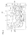
- Fig. 2 is a principal part cross sectional view about an embodiment of an image forming apparatus which comprises the electric charge eliminating device 110 relating to the present invention and an intermediate transfer belt 401 as an image carrying member of an electric charge elimination object.
- the following explanation will be made about an embodiment of a tandem type color image forming apparatus 400 as an image forming apparatus.
- a plurality of image forming members are arranged in parallel, and their structures and functions are as described below.
- the intermediate transfer belt 401 which is an intermediate transfer member, provided are four sets of process units 402Y, 402M, 402C, and 402K for forming four color toner images of yellow (Y), magenta (M), cyan (C), and black (K).
- Monochromatic toner images ofY, M, C, and K formed by the respective process units 402Y, 402M, 402C, and 402K are superimposed on the intermediate transfer belt 401, and the superimposed toner images are collectively transferred as a color image onto a recording sheet P.
- the color image is fixed on the recording sheet P, and is discharged outside the apparatus.
- an organic photoreceptor layer provided with an overcoat layer (protective layer) on its surface is formed on an outer periphery of a cylindrical metallic base member formed with, for example, aluminium.
- the intermediate transfer belt 401 being an image carrier is brought in contact with the photoreceptor drum 403 so that when the intermediate transfer belt 401 is shifted, the photoreceptor drum 403 is driven and rotated by receiving a driving force from the intermediate transfer belt 401, whereby the respective photoreceptor drums 403 for four colors are rotated in the direction indicated with an arrowed mark on the grounded condition.
- the scorotron charging unit 404 which is an electrically charging section for each color, performs an electrically charging action (in this embodiment, minus electrification) with corona discharge having the same polarity (in this embodiment, a minus polarity) with toner by a control grid and a corona discharge electrode which are maintained at a predetermined electric potential respectively. With this electrically charging action, the photoreceptor drum 403 is provided with a uniform electric potential.
- the scorotron charging unit 404 may employs a sawtooth-like electrode and a needlelike electrode as the corona discharge electrode.
- the exposure optical system 405, which is an image write-in section for each color ofY, M, and C and K, is arranged around the photoreceptor drum 403 such that its exposure position on the photoreceptor drum 403 for each color is located at the downstream side of the scorotron charging unit 404 in terms of the rotation direction of the photoreceptor drum 403.
- the exposure optical system 405 conducts image exposure for the photoconductive layer of the photoreceptor drum 403 in accordance with color image data of each color ofY, M, C, and K which have been read by an image reading apparatus in a separate body and are memorized in a memory, whereby an electrostatic latent image is formed on the photoreceptor drum 403 for each color.
- the developing unit 406 which is a developing section of each color ofY, M, and C and K, maintains a predetermined gap to the peripheral surface of the photoreceptor drum 403 as explained with reference Fig. 1 , and the developing unit 406 has a developing sleeve 406a rotated in the same direction with that of the photoreceptor drum 403.
- the developing sleeve 406a is structured with, for example, a cylinder made of nonmagnetic stainless steel or aluminium with a thickness of 0.5 to 1 mm and an outer diameter of 15 to and 25 mm.
- the developing agent is carried on the periphery of the developing sleeve 406a, and is made in a stand-up brush condition, whereby the developing unit 406 conducts a contact type reversal development so as to form a toner image on the photoreceptor drum 403.
- the developing unit 406 has a hopper 406b which supplies a two component type developer, and a recovery container 406c for collecting the two component type developer discharged from the developing unit 406, and the hopper and the recovery container are provided to the developing unit of each color of Y, M, and C and K.
- the concentration of toner of the two component type developer in the developing unit becomes low as the development progresses. Accordingly, the concentration of toner is detected by a toner concentration detection sensor 101c (refer to Fig.1 ) in the developing unit, and toner is supplied based on the detected information by the hopper through a supply pipe 406b1.
- the ratio of toner and carrier which constitute the two component type developer to be supplied is mixed such that it may become the ratio of toner and carrier in the developing unit on a normal state, and usually, toner is made large in content as compared with carrier.
- the supplied two component type developer is mixed and agitated with the used two component type developer in the developing unit.
- the amount of the two component type developer is detected by an interface level detecting section (not shown) provided in the developing unit, and when the surplus condition of the two component type developer is detected, the excess portion of the two component type developer is discharged to the outside of the developing unit by a discharging section such as a screw pump. In this way, the repetition of the supply and discharge makes it possible to stabilize the performance of the two component type developer in the developing unit.
- the respective process units 402Y, 402M, 402C, and 402K are arranged in parallel and opposite to the intermediate transfer belt 401, and this intermediate transfer belt 401 is an endless belt having a volume resistivity of 10 12 ⁇ cm to 10 15 ⁇ cm.
- the intermediate transfer belt 401 is produced such that for example, a conductive material is dispersed into engineering plastics, such as modified polyimide, a heat-curing polyimide, an ethylene tetrafluoroethylene copolymer, polyvinylidene fluoride, a nylon alloy and the like.
- the intermediate transfer belt 401 is a seamless belt with a two layer structure in which a fluorine coating is preferably formed with a thickness of 5 to 50 ⁇ m as a toner filming prevention layer on the outside of the semi conductive film base member with a thickness of 0.1 to 1.0mm.
- the base member of the intermediate transfer belt 401 in addition to the above, employed may be a semi conductive rubber belt with a thickness of 0.5 mm to 2.0 mm in which conductive materials are dispersed in a silicone rubber or a urethane rubber.
- the intermediate transfer belt 401 is stretched so as to circumscribe around a driving roller 401 a, a follower roller 401b, a tension roller 401 c, and a backup roller 401 d.
- the driving roller 401a is rotated by a driving motor (not shown) so that the intermediate transfer belt 401 is rotated in a direction indicated with a arrows mark while being pressed onto the photoreceptor drum 403 by a pressing elastic plate 401 e arranged at the upstream side of the transfer position of each color.
- the photoreceptor drums 403 are driven and rotated while following the shift of the intermediate transfer belt 401 by receiving a driving force of the intermediate transfer belt 401.
- Primary transfer devices 401f which are a transfer section for each color, include corona discharge devices, are arranged opposite to the respective photoreceptor drums 403 for each color across the intermediate transfer belt 401, and fonn the transfer area for each color between the intermediate transfer belt 401 and the respective photoreceptor drums 403 for colors ofY, M, C, and K.
- the primary transfer devices 401 fare applied with a direct current voltage with a opposite polarity to that of toner (in this embodiment, a plus polarity) so as to form a transfer electric field in the respective transfer areas, whereby a toner image on the photoreceptor drum 403 for each color is transferred on the intermediate transfer belt 401.
- Electric charge eliminating devices 401 g which are an electric charge eliminating section for each color, are constituted by a corona discharge device, and conduct electric charge elimination for the intermediate transfer belt 401 electrically charged by the primary transfer devices 401f.
- the pressing elastic plates 401 e to press the transfer belt are made of a rubber blade, such as urethane.
- the pressing elastic plate 401 e are arranged at the upstream side of the transfer position of each color. Therefore, at the time of forming an image, the pressing elastic plates 401 e press the intermediate transfer belt 401 onto the respective photoreceptor drums 403 so that the photoreceptor drums 403 are made to follow the shift of the intermediate transfer belt 401 and rotate.
- a photoreceptor driving motor (not shown) is started, toner images of colors ofY, M, C and K are formed on the photoreceptor drums 403, and then the toner images are sequentially transferred onto the intermediate transfer belt 401, whereby a superimposed color toner image ofY, M, C and K is formed.
- the recording sheet P on which a color toner image has been transferred is subjected to electric charge elimination by an electric charge eliminating electrode 410 which also acts a separating section, and then is conveyed to the fixing device 411.
- the fixing device 411 the recording sheet P is applied with heat and pressure between a fixing roller 411a and a pressing roller 411b so that the toner image is fixed onto the recording sheet P, thereafter, the recording sheet P is discharged onto a tray at the outside of the apparatus.
- the electric charge eliminating device 110 relating to the present invention is arranged at a position opposite to a follower roller 401b of a plurality of rollers around which the intermediate transfer belt 401 is wound and is adapted to eliminate a residual potential on the intermediate transfer belt 401.
- the residual toner after the transferring which remains on the intermediate transfer belt 401 is cleaned by a cleaning apparatus 412 being a cleaning section which is provided to be opposite to the follower roller 401b across the intermediate transfer belt 401.
- Fig. 3 is an outline structural view for explaining the structure of the first embodiment of the electric charge eliminating device 110 relating to the present invention
- Fig. 4a is a perspective view of Fig. 3
- Fig. 4b is a drawing viewed from an arrowed mark A in Fig. 3
- the electric charge eliminating device 110 is adapted to eliminate the residual potential on the transfer belt 6 wound around the support roller 62 in the abovementioned monochrome image forming apparatus 100 (refer to Fig. 1 ) or on the intermediate transfer belt 401 wound around the follower roller 401b in the color image forming apparatus 400 (refer to Fig. 2 ).
- the electric charge eliminating device 110 of the first embodiment comprises a needlelike electrode 111 connected to a discharging power source D 1 in which an AC voltage is superimposed on a DC voltage, an insulating holder 112 for holding the needlelike electrode 111, and a conductive shielding plate 113 as a shielding member arranged between the transfer belt 6 or the intermediate transfer belt 401 and the needlelike electrode 111.
- the conductive shielding plate 113 is grounded.
- the cover section 112a is located between the protruding sections 111a of the needlelike electrode 111 and the conductive shielding plate 113 so that cover section 112a prevents an excessive discharge current from the needlelike electrode 111 to the conductive shielding plate 113.
- the tip portions of the protruding sections 111a of the needlelike electrode 111 are arranged at the positions where the tip portions of the protruding sections 111a do not protrude from the tip 112b section of the cover section 112a.
- the plurality of partition wall sections 112c are formed at positions where two of the plurality of partition wall sections 112c sandwich one of the protruding sections 111a of the needlelike electrode 111, so that the plurality of partition wall sections 112c prevent an operator's hand from contacting the protruding sections 111a of the needlelike electrode 111 to which high voltage is applied.
- the conductive shielding plate 113 as a shielding member which has conductivity and relates to the present invention is arranged at a location where the conductive shielding plate 113 stands opposite the transfer belt 6 wound around the support roller 62 or the intermediate transfer belt 401 wound around the follower roller 401b.
- the support roller 62 and the follower roller 401b have a conductive cored metal bar respectively, an elastic layer is formed on the cored metal bar, and a resin coat layer having conductivity is formed as an outermost layer section.
- the support roller 62 and the follower roller 401b are structured with tree layers of the cored metal bar, the elastic layer, and the resin coat layer respectively. However, they may be structured with two layers without the elastic layer.
- a reference symbol "s" shown in Fig. 3 represents a tangent line which passes along the tip of the conductive shielding plate 113 and comes in contact with the surface of the transfer belt 6 wound around the support roller 62 or the surface of the intermediate transfer belt 401 wound around the follower roller 401b.
- Fig. 5 is an outline structural view for explaining the structure of the second embodiment of the electric charge eliminating device 110 relating to the present invention.
- the second embodiment is similar to the first embodiment, and the same reference symbol is given to a member having the same function. Therefore, an explanation for such a member is omitted, and only a different structure is explained.
- the point that the second embodiment differs from the first embodiment is the difference in the member connected to the conductive shielding plate 113. That is, in the first embodiment, the member connected to the conductive shielding plate. 113 is only the grounding.
- a bias power source D2 as a power source for shielding member is connected to the conductive shielding plate 113.
- an electric potential of-300 V is provided to the power source D2 so that a part of minus current due to the discharge from the needlelike electrode 111 is made to flow to the ground through the conductive shielding plate 113, whereby an excessive current can be prevented from flowing into the transfer belt 6 or the intermediate transfer belt 401.
- discharge unevenness caused by the needlelike electrode 111 can be adjusted finely in accordance with conditions, such as an environmental condition and the working hours of an apparatus.
- the third through sixth embodiments of the electric charge eliminating device 110 relating to the present invention will be explained.
- the third through sixth embodiments are similar to the second embodiment, and the same reference symbol is given to a member having the same function. Therefore, an explanation for such a member is omitted, and only a different structure is explained.
- the point that the third through sixth embodiments differ from the second embodiment is the difference in the member connected to the conductive shielding plate 113. That is, in the second embodiment, the member connected to the conductive shielding plate 113 is the bias power source D2.
- respective different electric components are connected as a member to control a current flowing into the conductive shielding plate 113. Namely, in the third embodiment, a resister T is connected, in the fourth embodiment, a valuable resister KT is connected, in the fifth embodiment, a varistor VR is connected, and in the sixth embodiment, a zener diode ZD is connected.
- Fig. 6 is an outline structural view for explaining the structure of the third embodiment of the electric charge eliminating device 110 relating to the present invention.
- a resister T is used as an electric component connected to the conductive shielding plate 113.
- discharge unevenness of the needlelike electrode 111 can be adjusted with the simple structure to connect the resister T to the conductive shielding plate 113, whereby the discharge unevenness preventive measures can be achieved at low cost with space saving.
- Fig. 7 is an outline structural view for explaining the structure of the fourth embodiment of the electric charge eliminating device 110 relating to the present invention.
- a variable resister KT is used as an electric component connected to the conductive shielding plate 113.
- the structure to connect the variable resister KT to the conductive shielding plate 113 makes it possible to control the value of the provided voltage, whereby discharge unevenness can be adjusted in accordance with conditions, such as an environmental condition and the working hours of an apparatus.
- Fig. 8 is an outline structural view for explaining the structure of the fifth embodiment of the electric charge eliminating device 110 relating to the present invention.
- a varistor VR is used as an electric component connected to the conductive shielding plate 113.
- the structure to connect the varistor VR to the conductive shielding plate 113 makes it easy to maintain the value of the voltage of the conductive shielding plate 113, whereby the discharge unevenness preventive measures can be achieved precisely.
- Fig. 9 is an outline structural view for explaining the structure of the sixth embodiment of the electric charge eliminating device 110 relating to the present invention.
- a zener diode ZD is used as an electric component connected to the conductive shielding plate 113.
- the change of the connection direction of the zener diode ZD makes it possible to change the polarity of an electric potential provided to the conductive shielding plate 113.
- the structure to connect the zener diode ZD to the conductive shielding plate 113 makes it possible to provide an electric potential different in polarity in accordance with the polarity of the residual electric charge on the transfer belt 6 or the intermediate transfer belt 401. Namely, in accordance with the polarity of the residual electric charge on the transfer belt 6 or the intermediate transfer belt 401, an electric potential with the corresponding polarity can be made to flow through the conductive shielding plate 113, whereby, even if the polarity of a residual electric charge is any one of plus and minus, the residual electric charge can be eliminated precisely.
- Fig.10 is an outline structural view for explaining the structure of the seventh embodiment of the electric charge eliminating device 110 relating to the present invention.
- the seventh embodiment is similar to the first through sixth embodiments, and the same reference symbol is given to a member having the same function. Therefore, an explanation for such a member is omitted, and only a different structure is explained.
- the point that the seventh embodiment differs from the first through sixth embodiments is in the configuration of the conductive shielding plate 113. That is, in the first through sixth embodiments, the configuration of the conductive shielding plate 113 is a flat plate. However, in the seventh embodiment, it is formed by a wavelike plate member with a continuous concavo-convex curved surface.
- the pitch of the convex portions or the concave portions of the wavelike plate member forming the conductive shielding plate 113 conforms to that of the protruding sections 111a of the needlelike electrode 111, and the concave portions of the wavelike plate member are arranged opposite to the protruding sections 111a.
- the tips of the protruding sections 111a of the needlelike electrode 111 are located in the inside (the lower side in Fig. 3 ) in relation to the tangent line "s" which passes along the tip of the conductive shielding plate 113 and comes in contact with the surface of the transfer belt 6 or the surface of the intermediate transfer belt 401. Therefore, the position of the convex portions of the wavelike plate member of the conductive shielding plate 113 becomes close to the tip of the protruding sections 111a of the needlelike electrode 111 and the position of the concave portions becomes far from the tip of the protruding sections 111a.
- a current component is intercepted by the concave portions located at a more distant position on the wavelike plate member and tends to flow easily along the conductive shielding plate 113, so that a current component arriving to the transfer belt 6 or the intermediated transfer belt 401 becomes small.
- a current component passes over the convex portions located at a more close position on the wavelike plate member, so that a current component arriving to the transfer belt 6 or the intermediated transfer belt 401 becomes large.
- the seventh embodiment of the electric charge eliminating device 110 relating to the present invention with the employment of the conductive shielding plate 113 formed by a wavelike plate member, discharge unevenness can be suppressed with a simple structure.
- Fig.11 is an outline structural view for explaining the structure of the eighth embodiment of the electric charge eliminating device 110 relating to the present invention.
- the eighth embodiment is similar to the seventh embodiment, and the same reference symbol is given to a member having the same function. Therefore, an explanation for such a member is omitted, and only a different structure is explained.
- the point that the seventh embodiment differs from the first through sixth embodiments is in the configuration of the conductive shielding plate 113. That is, in the seventh embodiment, the configuration of the conductive shielding plate 113. is a wavelike plate member. However, in the eighth embodiment, a material with a high resistance is coated or pasted in a wavelike form (a black solid portion in Fig. 11 ).
- the pitch of the convex portions or the concave portions of the wavelike curve is adapted to conform to that of the protruding sections 111a of the needlelike electrode 111 and the concave portions of the wavelike curve are formed so as to be opposite to the protruding sections 111a of the needlelike electrode 111. Therefore, as with the seventh embodiment, among the current discharged from the tips of the protruding sections 111 a, in the vicinity of the protruding sections 111a of the needlelike electrode 111, many currents flow along the conductive shielding plate 113, and in the vicinity of the valley portion between the protruding sections 111a, many currents flow onto the transfer belt 6 or the intermediated transfer belt 401. With this, discharge unevenness due to the protruding sections 111a of the needlelike electrode 111 can be suppressed.
- the eighth embodiment of the electric charge eliminating device 110 relating to the present invention with the employment of the conductive shielding plate 113 formed by a material coated or pasted in a wavelike form, discharge unevenness can be suppressed with a simple structure.
- Fig.12 is a partial cross sectional view for explaining the positional relationship of the needlelike electrode 111, the insulating holder 112, and the conductive shielding plate 113 in the electric charge eliminating device 110 relating to the present invention. Since the positional relationship of the needlelike electrode 111, the insulating holder 112 and the conductive shielding plate 113 for the transfer belt 6 or the intermediate transfer belt 401 has been already explained in Fig. 3 , the explanation for it is omitted here.
- a reference symbol “a” represents a straight line which connects the tip of the needlelike electrode 111 and the tip 112b of the insulating holder 112 with the shortest distance
- a reference symbol “Q” represents an arbitrary point that the straight line “a” intersects the surface of the conductive shielding plate 113.
- a reference symbol “L” represents a shortest air space distance between the tip of the needlelike electrode 111 and the point Q where the straight line "a” intersects with the conductive shielding plate 113.
- a reference symbol “d” represents a holder-to-shielding plate gap between the tip 112b of the cover section 112a of the insulating holder 112 and the surface of the conductive shielding plate 113.
- each of the needlelike electrode 111, the insulating holder 112 and the conductive shielding plate 113 are set up such that the extension line of the straight line "a" intersects necessarily on the conductive shielding plate 113 (at the crossing point Q).
- the tip position of the needlelike electrode 111 is arranged at a position where the tip does not protrude from the tip position of the cover section 112a of the insulating holder 112.
- the conductive shielding plate 113 is adapted to have a region of an unexposed portion where the conductive shielding plate 113 is covered with the cover section 112a of the insulating holder 112 and a region of an exposed portion where the conductive shielding plate 113 is not covered with the cover section 112a.
- the electric field is formed by the needlelike electrode 111 toward the region of the exposed portion on the conductive shielding plate 113 which locates from the neighborhood of the point "Q" where the straight line intersects with the conductive shielding plate 113 to the tip of the conductive shielding plate 11.
- the present inventors have grasped through an experiment that the proper setting of the shortest air space distance "L” and the holder-to-shielding plate gap “d” makes it possible to prevent discharge unevenness by a needlelike electrode in the electric charge eliminating device which employs an intermediate transfer belt or transfer belt each made of resin.
- the value of the shortest air space distance "L” is set to 1.5 to 5.5 mm and the value of the holder-to-shielding plate gap "d” is set to 0.3 to 2.0 mm
- an influence due to discharge unevenness can be made to be not caused on a transfer belt 6, an intermediate transfer belt 401 or a roller around which a belt is wound.
- the influence due to discharge unevenness the occurrence of streak like flows caused by breakage of polymer chain of a resin material for a belt and peel-off of a resin coat layer for a roller around which a belt is wound.
- an electric charge eliminating device including a needlelike electrode and an image forming apparatus which eliminates electric charge on an image carrier or a recording media carrier without unevenness and does not cause cleaning failure and image failure without increasing the capacity and size of a power source.
Landscapes
- Physics & Mathematics (AREA)
- General Physics & Mathematics (AREA)
- Electrostatic Charge, Transfer And Separation In Electrography (AREA)
- Control Or Security For Electrophotography (AREA)
- Elimination Of Static Electricity (AREA)
- Discharging, Photosensitive Material Shape In Electrophotography (AREA)
Abstract
Description
- This application is based on Japanese Patent Application No.
2009-247573 filed on October 28, 2009 - The present invention relates to an electric charge eliminating device which eliminates electric charge on an image carrier used for an image forming apparatus of an electro-photographic system, or on a recording medium carrier, and relates to an image forming, apparatus equipped with the electric charge eliminating device.
- Conventionally, as an electric charge eliminating device which eliminates electric charge on an image carrier used for an image forming apparatus of an electro-photographic system, or on a recording medium carrier, usually used is a type which provides a high voltage to a wire electrode. In addition, another type that employs a needlelike (sawtooth like) electrode is also used in order to reduce ozone evolution and to save space.
- However, in the type employing a needlelike electrode, there is a difference in electric-field strength between an electric field on a tip portion being a discharge point of a needlelike electrode and an electric field on a middle point to the adjoining tip portion, whereby discharge unevenness tends to take place. Further, in many cases of electric charge eliminating devices employing needlelike electrodes, in order to prevent the contact to a sharp tip portion, a rib-shaped partition wall made of insulating materials such as resin is used for the tip portion of a needlelike electrode. With this partition wall, discharge unevenness tends to take place more easily. If the whole electric field is strengthened too much in order to prevent poor electric charge elimination due to discharge unevenness, discharge at the tip portion of a needlelike electrode becomes strong too much, and the strong discharge causes discharge deterioration on the surface of an image carrier or a recording medium carrier for which electric charge elimination is conducted. As a result, there is a problem that poor cleaning and inferior transfer tend to occur easily.
- Specifically, in an electric charge eliminating device having a structure that employs an intermediate transfer belt or a transfer belt made of resin as an image carrier or a recording medium carrier, there may be a case where polymer chains of resin materials are broken due to discharge unevenness such that whitened streaks-like flaws are caused on the surface. Further, in the case where a roller having a conductive resin coat layer is used as a roller around which an intermediate transfer belt or a transfer belt is wound, there is a problem that the resin coat layer is peeled off due to discharge unevenness of a needlelike electrode and the peeled-off resin coat layer adheres on the reverse surface of the belt. This peeling-off of the resin coat layer of the roller deteriorates the conductivity of a roller and the performance of a belt, and becomes a factor to worsen more the discharge deterioration of the intermediate transfer belt or the transfer belt
- In order to prevent such discharge unevenness, disclosed is a technique in which an insulating member is provided between an image carrier or a recording medium carrier and a needlelike electrode such that air clearance is created so as to prevent the discharge deterioration of the image carrier or the recording medium carrier (for example, refer to Japanese Unexamined Patent Publication No.
2005-181863 - However, if an tip member of a needlelike electrode is surrounded with an insulating member, the electric charge eliminating capacity becomes lower due to the lowering of the discharge effect. As a result, caused are separate fault of thin paper sheets, image defects accompanying toner scattering due to separation discharge at the time of the separating of recording medium. Further, in order to prevent discharge unevenness, if the distance between the tip portion of an electrode and an image carrier or a recording medium carrier is made longer, it is required to use a high voltage power source with a further more large capacity. As a result, caused is a new problem in terms of power consumption and space saving.
- An object of the present invention is to solve the above problems and to provide an electric charge eliminating device which eliminates properly electric charges on an image carrier or a recording medium carrier without increasing the capacity and size of a power source and does not cause poor cleaning nor image defects, and to provide an image forming apparatus equipped with the electric charge eliminating device.
- The abovementioned object is attained by the structure that reflects an aspect of the present invention.
- An electric charge eliminating device for eliminating electric charge on an image carrying member or on a recording medium carrying member which is incorporated in an image forming apparatus, comprises:
- a needlelike electrode having a plurality of protruding sections which form a plurality of discharge points;
- an insulating holder for holding the needlelike electrode;
- a discharging power source for applying an electric voltage to the needlelike electrode; and
- a conductive shielding member arranged between the needlelike electrode and the image carrying member or the recording medium carrying member.
- An other aspect of the invention provides an image forming apparatus, including an electric charge eliminating device according to an aspect of the invention.
-
-
Fig. 1 is a principal part cross sectional view about an embodiment of an image forming apparatus equipped with an electriccharge eliminating device 110 relating to the present invention and atransfer belt 6 as a recording medium carrier being an electric charge elimination object. -
Fig. 2 is a principal part cross sectional view about an embodiment of an image forming apparatus comprising an electriccharge eliminating device 110 relating to the present invention and anintermediate transfer belt 401 as a recording medium carrier being an electric charge elimination object. -
Fig. 3 is an outline structural view for explaining a structure of the first embodiment of the electriccharge eliminating device 110 relating to the present invention. -
Fig. 4a is a perspective view ofFig. 3 andFig. 4b is a drawing viewed from an arrowed mark A. -
Fig. 5 is an outline structural view for explaining a structure of the second embodiment of the electriccharge eliminating device 110 relating to the present invention. -
Fig. 6 is an outline structural view for explaining a structure of the third embodiment of the electriccharge eliminating device 110 relating to the present invention. -
Fig. 7 is an outline structural view for explaining a structure of the fourth embodiment of the electriccharge eliminating device 110 relating to the present invention. -
Fig. 8 is an outline structural view for explaining a structure of the fifth embodiment of the electriccharge eliminating device 110 relating to the present invention. -
Fig. 9 is an outline structural view for explaining a structure of the sixth embodiment of the electriccharge eliminating device 110 relating to the present invention. -
Fig.10 is an outline structural view for explaining a structure of the seventh embodiment of the electriccharge eliminating device 110 relating to the present invention. -
Fig.11 is an outline structural view for explaining a structure of the eighth embodiment of the electriccharge eliminating device 110 relating to the present invention. -
Fig.12 is a fragmentary sectional view for explaining the positional relationship among theneedlelike electrode 111, theinsulating holder 112, and theconductive shielding plate 113 in the electriccharge eliminating device 110 relating to the present invention. - Hereafter, an embodiment of the present invention will be explained with reference to drawings. However, the present invention is not restricted to such an embodiment.
-
Fig. 1 is a principal part cross sectional view about an embodiment of an image forming apparatus equipped with an electriccharge eliminating device 110 relating to the present invention and atransfer belt 6 as a recording medium carrier of an electric charge elimination object. In this drawing, an embodiment of a monochromeimage forming apparatus 100 as an image forming apparatus will be explained. - In
Fig. 1 ,numeral 1 is a photoreceptor drum as an image forming member, and theimage forming apparatus 100 comprises, along the rotation direction of thisphotoreceptor drum 1, anelectrification charger 2; an image write-indevice 3 with a LED light source; a developing device 4 with a two component system; and a recoding sheet guide to lead a recording sheet P as a recording medium to a transfer region. Further, theimage forming apparatus 100 comprises a transfer belt as an image carrier to transfer a toner image formed on thephotoreceptor drum 1 to a recording sheet P; acleaning device 7 to clean thephotoreceptor drum 1 with brush and blade; aerasing device 8 to erase electric charge by irradiating a erasing light beam on thephotoreceptor 1. Furthermore, between thetransfer belt 6 and thecleaning device 7, apreliminary cleaning charger 9 is provided, and at the downstream side of thetransfer belt 6, afixing device 10 is provided so as to fix a toner image on a recording sheet P. - The developing device 4 has a developing
sleeve 41 in an opening section of ahousing 40, and at the backward of the developing sleeve 41 (in the right direction in the drawing), a developer conveyance member42 to convey a developer (toner and carrier) to the developingsleeve 41 and an agitating member43 to agitate toner and carrier are arranged. - The
transfer belt 6 is stretched over between two supportingrollers photoreceptor drum 1 by abackup roller 63 provided between thesupport rollers transfer belt 6. Thetransfer belt 6 is structured with two layers of a semi-conductive belt base material and an insulating resin layer which is provided as a surface layer and has a volume resistivity more of 1x10⁷ Ωcm or more, and the insulating resin layer being a surface layer is formed by coating or pasting. As the belt base material, for example, rubber base materials, such as chloroprene, may be employed, and as the insulating layer, a tetrafluoroethylene perfluoroalkyl vinyl ether copolymer resin (PFA) and the like may be employed. - Although the
transfer belt 6 is made in the two layer structure in this embodiment, it also may be a resin-made belt composed of a single layer of only a belt base material. - An electric
charge eliminating device 110 relating to the present invention is arranged opposite to a supportingroller 62 which is one of two supportingrollers transfer belt 6 is wound, and the electriccharge eliminating device 110 eliminates a residual electric potential on thetransfer belt 6 after the transferring of a toner image. - The
backup roller 63 is connected to a constant current power source 64 in which an applying timing and an amount of current are controlled by a control section 11. - A
pre cleaning charger 9 is a corotron type charger, and its electrode is connected to a constant current power source 90 in which an applying timing and an amount of current are controlled by the control section 11. In addition to the applying of current to thetransfer belt 6 and thepre cleaning charger 9, the control section 11 controls respective process sections so as to perform an image formation. -
Fig. 2 is a principal part cross sectional view about an embodiment of an image forming apparatus which comprises the electriccharge eliminating device 110 relating to the present invention and anintermediate transfer belt 401 as an image carrying member of an electric charge elimination object. With regard to this figure, the following explanation will be made about an embodiment of a tandem type colorimage forming apparatus 400 as an image forming apparatus. - In the color
image forming apparatus 400, a plurality of image forming members are arranged in parallel, and their structures and functions are as described below. Around the periphery of theintermediate transfer belt 401 which is an intermediate transfer member, provided are four sets ofprocess units respective process units intermediate transfer belt 401, and the superimposed toner images are collectively transferred as a color image onto a recording sheet P. The color image is fixed on the recording sheet P, and is discharged outside the apparatus. -
Numeral 403 represents a photoreceptor drum which is an image forming member, and is arranged for each color ofY, M, and C and K. On the periphery of thephotoreceptor drum 403, arranged are ascorotron charging unit 404 which is an electrically charging section, an exposureoptical system 405 which is an image write-in section, a developingunit 406, and acleaning device 407 which is a cleaning sections of thephotoreceptor drum 403. These components are provided for therespective photoreceptor drums 403 provided for the colors ofY, M, and C and K. - In the
respective photoreceptor drums 403 which are image forming members for colors ofY, M, and C and K, an organic photoreceptor layer (OPC) provided with an overcoat layer (protective layer) on its surface is formed on an outer periphery of a cylindrical metallic base member formed with, for example, aluminium. Theintermediate transfer belt 401 being an image carrier is brought in contact with thephotoreceptor drum 403 so that when theintermediate transfer belt 401 is shifted, thephotoreceptor drum 403 is driven and rotated by receiving a driving force from theintermediate transfer belt 401, whereby therespective photoreceptor drums 403 for four colors are rotated in the direction indicated with an arrowed mark on the grounded condition. - The
scorotron charging unit 404, which is an electrically charging section for each color, performs an electrically charging action (in this embodiment, minus electrification) with corona discharge having the same polarity (in this embodiment, a minus polarity) with toner by a control grid and a corona discharge electrode which are maintained at a predetermined electric potential respectively. With this electrically charging action, thephotoreceptor drum 403 is provided with a uniform electric potential. Thescorotron charging unit 404 may employs a sawtooth-like electrode and a needlelike electrode as the corona discharge electrode. - The exposure
optical system 405, which is an image write-in section for each color ofY, M, and C and K, is arranged around thephotoreceptor drum 403 such that its exposure position on thephotoreceptor drum 403 for each color is located at the downstream side of thescorotron charging unit 404 in terms of the rotation direction of thephotoreceptor drum 403. The exposureoptical system 405 conducts image exposure for the photoconductive layer of thephotoreceptor drum 403 in accordance with color image data of each color ofY, M, C, and K which have been read by an image reading apparatus in a separate body and are memorized in a memory, whereby an electrostatic latent image is formed on thephotoreceptor drum 403 for each color. - The developing
unit 406, which is a developing section of each color ofY, M, and C and K, maintains a predetermined gap to the peripheral surface of thephotoreceptor drum 403 as explained with referenceFig. 1 , and the developingunit 406 has a developingsleeve 406a rotated in the same direction with that of thephotoreceptor drum 403. The developingsleeve 406a is structured with, for example, a cylinder made of nonmagnetic stainless steel or aluminium with a thickness of 0.5 to 1 mm and an outer diameter of 15 to and 25 mm. The developingunit 406 accommodates a two component type developing agent of one of yellow (Y), magenta (M), cyan (C), and black (K) corresponding to one of developing colors ofY, M, C and K. In the developingunit 406, a gap between the developingsleeve 406a and thephotoreceptor drum 403 is maintained at a predetermined value of, for example, 100 µm to 500 µm with a spacing roller (not shown), and the developingsleeve 406a is applied with a developing bias which is a direct current voltage or a direct current voltage superimposed with an alternating current voltage. With this, the developing agent is carried on the periphery of the developingsleeve 406a, and is made in a stand-up brush condition, whereby the developingunit 406 conducts a contact type reversal development so as to form a toner image on thephotoreceptor drum 403. - Further, the developing
unit 406 has ahopper 406b which supplies a two component type developer, and a recovery container 406c for collecting the two component type developer discharged from the developingunit 406, and the hopper and the recovery container are provided to the developing unit of each color of Y, M, and C and K. As explained with reference toFig. 1 , the concentration of toner of the two component type developer in the developing unit becomes low as the development progresses. Accordingly, the concentration of toner is detected by a toner concentration detection sensor 101c (refer toFig.1 ) in the developing unit, and toner is supplied based on the detected information by the hopper through a supply pipe 406b1. - The ratio of toner and carrier which constitute the two component type developer to be supplied is mixed such that it may become the ratio of toner and carrier in the developing unit on a normal state, and usually, toner is made large in content as compared with carrier.
- The supplied two component type developer is mixed and agitated with the used two component type developer in the developing unit. The amount of the two component type developer is detected by an interface level detecting section (not shown) provided in the developing unit, and when the surplus condition of the two component type developer is detected, the excess portion of the two component type developer is discharged to the outside of the developing unit by a discharging section such as a screw pump. In this way, the repetition of the supply and discharge makes it possible to stabilize the performance of the two component type developer in the developing unit.
- On the
photoreceptor drum 403 which is uniformly electrically charged by thescorotron charging unit 404, image exposure is performed by the exposureoptical system 405 so that an electrostatic latent image is formed, and the electrostatic latent image is developed by the developingunit 406, whereby a toner image is formed. This toner image is transferred onto theintermediate transfer belt 401 at a transfer position. After the toner image has been transferred, the remaining toner on thephotoreceptor drum 403 is cleaned by thecleaning apparatus 407 which conducts collecting the remaining toner electro-statically. - The
respective process units intermediate transfer belt 401, and thisintermediate transfer belt 401 is an endless belt having a volume resistivity of 1012 Ωcm to 1015 Ωcm. Theintermediate transfer belt 401 is produced such that for example, a conductive material is dispersed into engineering plastics, such as modified polyimide, a heat-curing polyimide, an ethylene tetrafluoroethylene copolymer, polyvinylidene fluoride, a nylon alloy and the like. Theintermediate transfer belt 401 is a seamless belt with a two layer structure in which a fluorine coating is preferably formed with a thickness of 5 to 50 µm as a toner filming prevention layer on the outside of the semi conductive film base member with a thickness of 0.1 to 1.0mm. As the base member of theintermediate transfer belt 401, in addition to the above, employed may be a semi conductive rubber belt with a thickness of 0.5 mm to 2.0 mm in which conductive materials are dispersed in a silicone rubber or a urethane rubber. Theintermediate transfer belt 401 is stretched so as to circumscribe around a drivingroller 401 a, afollower roller 401b, atension roller 401 c, and abackup roller 401 d. At the time of forming an image, the drivingroller 401a is rotated by a driving motor (not shown) so that theintermediate transfer belt 401 is rotated in a direction indicated with a arrows mark while being pressed onto thephotoreceptor drum 403 by a pressingelastic plate 401 e arranged at the upstream side of the transfer position of each color. At this time, the photoreceptor drums 403 are driven and rotated while following the shift of theintermediate transfer belt 401 by receiving a driving force of theintermediate transfer belt 401. -
Primary transfer devices 401f, which are a transfer section for each color, include corona discharge devices, are arranged opposite to therespective photoreceptor drums 403 for each color across theintermediate transfer belt 401, and fonn the transfer area for each color between theintermediate transfer belt 401 and therespective photoreceptor drums 403 for colors ofY, M, C, and K. Theprimary transfer devices 401 fare applied with a direct current voltage with a opposite polarity to that of toner (in this embodiment, a plus polarity) so as to form a transfer electric field in the respective transfer areas, whereby a toner image on thephotoreceptor drum 403 for each color is transferred on theintermediate transfer belt 401. - Electric
charge eliminating devices 401 g, which are an electric charge eliminating section for each color, are constituted by a corona discharge device, and conduct electric charge elimination for theintermediate transfer belt 401 electrically charged by theprimary transfer devices 401f. - The pressing
elastic plates 401 e to press the transfer belt are made of a rubber blade, such as urethane. The pressingelastic plate 401 e are arranged at the upstream side of the transfer position of each color. Therefore, at the time of forming an image, the pressingelastic plates 401 e press theintermediate transfer belt 401 onto therespective photoreceptor drums 403 so that the photoreceptor drums 403 are made to follow the shift of theintermediate transfer belt 401 and rotate. - When an image recording is started, a photoreceptor driving motor (not shown) is started, toner images of colors ofY, M, C and K are formed on the photoreceptor drums 403, and then the toner images are sequentially transferred onto the
intermediate transfer belt 401, whereby a superimposed color toner image ofY, M, C and K is formed. - In synchronization with the color toner image formation superimposed on the
intermediate transfer belt 401, a recording sheet P is conveyed from apaper sheet cassette 408 being a transfer material storage section, through atiming roller 409 as a transfer material feeding section to a transfer area (with no reference symbol) of asecondary transfer device 401h being a second transfer section. Then, thesecondary transfer device 40 1 h is applied with a direct current voltage with a reverse polarity (in this embodiment, a plus polarity) to that of toner, whereby the superimposed color toner image on theintermediate transfer belt 401 is collectively transferred onto the recording sheet P. - After the toner images have been transferred, residual toners remained on the peripheral surfaces of the photoreceptor drums 403 for colors ofY, M, and C, and K are cleaned by the
cleaning devices 407 which are a cleaning section for the image forming member of each color. - The recording sheet P on which a color toner image has been transferred is subjected to electric charge elimination by an electric
charge eliminating electrode 410 which also acts a separating section, and then is conveyed to thefixing device 411. In thefixing device 411, the recording sheet P is applied with heat and pressure between a fixingroller 411a and apressing roller 411b so that the toner image is fixed onto the recording sheet P, thereafter, the recording sheet P is discharged onto a tray at the outside of the apparatus. - The electric
charge eliminating device 110 relating to the present invention is arranged at a position opposite to afollower roller 401b of a plurality of rollers around which theintermediate transfer belt 401 is wound and is adapted to eliminate a residual potential on theintermediate transfer belt 401. - After a color toner image has been transferred, the residual toner after the transferring which remains on the
intermediate transfer belt 401 is cleaned by acleaning apparatus 412 being a cleaning section which is provided to be opposite to thefollower roller 401b across theintermediate transfer belt 401. -
Fig. 3 is an outline structural view for explaining the structure of the first embodiment of the electriccharge eliminating device 110 relating to the present invention,Fig. 4a is a perspective view ofFig. 3 , andFig. 4b is a drawing viewed from an arrowed mark A inFig. 3 . The electriccharge eliminating device 110 is adapted to eliminate the residual potential on thetransfer belt 6 wound around thesupport roller 62 in the abovementioned monochrome image forming apparatus 100 (refer toFig. 1 ) or on theintermediate transfer belt 401 wound around thefollower roller 401b in the color image forming apparatus 400 (refer toFig. 2 ). - The electric
charge eliminating device 110 of the first embodiment comprises aneedlelike electrode 111 connected to a dischargingpower source D 1 in which an AC voltage is superimposed on a DC voltage, an insulatingholder 112 for holding theneedlelike electrode 111, and aconductive shielding plate 113 as a shielding member arranged between thetransfer belt 6 or theintermediate transfer belt 401 and theneedlelike electrode 111. In the first embodiment, theconductive shielding plate 113 is grounded. - As shown in
Fig. 4b , theneedlelike electrode 111 of the present invention is formed by a platelike conductive member which includes a plurality of interlinked sawtooth-like (or needlelike) protrusions 111a, and the tip ends of the plurality of protrudingsections 111a woke as a plurality of discontinuous discharge points. Theneedlelike electrode 111 is connected to the dischargingpower source D 1 as a power source for discharge. In the vicinity of the protrudingsections 111a of theneedlelike electrode 111 on the insulatingholder 112 holding theneedlelike electrode 111, formed are acover section 112a, atip section 112b, and a plurality ofpartition wall sections 112c. Thecover section 112a is located between the protrudingsections 111a of theneedlelike electrode 111 and theconductive shielding plate 113 so thatcover section 112a prevents an excessive discharge current from theneedlelike electrode 111 to theconductive shielding plate 113. The tip portions of the protrudingsections 111a of theneedlelike electrode 111 are arranged at the positions where the tip portions of the protrudingsections 111a do not protrude from thetip 112b section of thecover section 112a. The plurality ofpartition wall sections 112c are formed at positions where two of the plurality ofpartition wall sections 112c sandwich one of the protrudingsections 111a of theneedlelike electrode 111, so that the plurality ofpartition wall sections 112c prevent an operator's hand from contacting the protrudingsections 111a of theneedlelike electrode 111 to which high voltage is applied. - The
conductive shielding plate 113 as a shielding member which has conductivity and relates to the present invention is arranged at a location where theconductive shielding plate 113 stands opposite thetransfer belt 6 wound around thesupport roller 62 or theintermediate transfer belt 401 wound around thefollower roller 401b. - The
support roller 62 and thefollower roller 401b have a conductive cored metal bar respectively, an elastic layer is formed on the cored metal bar, and a resin coat layer having conductivity is formed as an outermost layer section. In this embodiment, thesupport roller 62 and thefollower roller 401b are structured with tree layers of the cored metal bar, the elastic layer, and the resin coat layer respectively. However, they may be structured with two layers without the elastic layer. - A reference symbol "s" shown in
Fig. 3 represents a tangent line which passes along the tip of theconductive shielding plate 113 and comes in contact with the surface of thetransfer belt 6 wound around thesupport roller 62 or the surface of theintermediate transfer belt 401 wound around thefollower roller 401b. - When the discharge from the protruding
sections 111a of theneedlelike electrode 111 is started with the voltage applied from the power source D1, a part of excessive discharge current generated from the protrudingsections 111a flows into the ground via theconductive shielding plate 113, whereby discharge unevenness can be suppressed. - According to the first embodiment of the electric
charge eliminating device 110 relating to the present invention, the excessive discharge current generated from the protrudingsections 111a of theneedlelike electrode 111 can be made to flow through theconductive shielding plate 113 with the simple structure to ground theconductive shielding plate 113, whereby the discharge unevenness preventive measures can be achieved at low cost. -
Fig. 5 is an outline structural view for explaining the structure of the second embodiment of the electriccharge eliminating device 110 relating to the present invention. The second embodiment is similar to the first embodiment, and the same reference symbol is given to a member having the same function. Therefore, an explanation for such a member is omitted, and only a different structure is explained. The point that the second embodiment differs from the first embodiment is the difference in the member connected to theconductive shielding plate 113. That is, in the first embodiment, the member connected to the conductive shielding plate. 113 is only the grounding. However, in the second embodiment, a bias power source D2 as a power source for shielding member is connected to theconductive shielding plate 113. In this embodiment, an electric potential of-300 V is provided to the power source D2 so that a part of minus current due to the discharge from theneedlelike electrode 111 is made to flow to the ground through theconductive shielding plate 113, whereby an excessive current can be prevented from flowing into thetransfer belt 6 or theintermediate transfer belt 401. - According to the second embodiment of the electric
charge eliminating device 110 relating to the present invention, since it is possible to control the polarity of an electric potential and a value of a voltage to be provided, discharge unevenness caused by theneedlelike electrode 111 can be adjusted finely in accordance with conditions, such as an environmental condition and the working hours of an apparatus. - Hereafter, the third through sixth embodiments of the electric
charge eliminating device 110 relating to the present invention will be explained. However, the third through sixth embodiments are similar to the second embodiment, and the same reference symbol is given to a member having the same function. Therefore, an explanation for such a member is omitted, and only a different structure is explained. The point that the third through sixth embodiments differ from the second embodiment is the difference in the member connected to theconductive shielding plate 113. That is, in the second embodiment, the member connected to theconductive shielding plate 113 is the bias power source D2. However, in the third through sixth embodiments, respective different electric components are connected as a member to control a current flowing into theconductive shielding plate 113. Namely, in the third embodiment, a resister T is connected, in the fourth embodiment, a valuable resister KT is connected, in the fifth embodiment, a varistor VR is connected, and in the sixth embodiment, a zener diode ZD is connected. -
Fig. 6 is an outline structural view for explaining the structure of the third embodiment of the electriccharge eliminating device 110 relating to the present invention. In the third embodiment, a resister T is used as an electric component connected to theconductive shielding plate 113. - According to the third embodiment of the electric
charge eliminating device 110 relating to the present invention, discharge unevenness of theneedlelike electrode 111 can be adjusted with the simple structure to connect the resister T to theconductive shielding plate 113, whereby the discharge unevenness preventive measures can be achieved at low cost with space saving. -
Fig. 7 is an outline structural view for explaining the structure of the fourth embodiment of the electriccharge eliminating device 110 relating to the present invention. In the fourth embodiment, a variable resister KT is used as an electric component connected to theconductive shielding plate 113. - According to the fourth embodiment of the electric
charge eliminating device 110 relating to the present invention, the structure to connect the variable resister KT to theconductive shielding plate 113 makes it possible to control the value of the provided voltage, whereby discharge unevenness can be adjusted in accordance with conditions, such as an environmental condition and the working hours of an apparatus. -
Fig. 8 is an outline structural view for explaining the structure of the fifth embodiment of the electriccharge eliminating device 110 relating to the present invention. In the fifth embodiment, a varistor VR is used as an electric component connected to theconductive shielding plate 113. - According to the fifth embodiment of the electric
charge eliminating device 110 relating to the present invention, the structure to connect the varistor VR to theconductive shielding plate 113 makes it easy to maintain the value of the voltage of theconductive shielding plate 113, whereby the discharge unevenness preventive measures can be achieved precisely. -
Fig. 9 is an outline structural view for explaining the structure of the sixth embodiment of the electriccharge eliminating device 110 relating to the present invention. In the sixth embodiment, a zener diode ZD is used as an electric component connected to theconductive shielding plate 113. The change of the connection direction of the zener diode ZD makes it possible to change the polarity of an electric potential provided to theconductive shielding plate 113. - According to the sixth embodiment of the electric
charge eliminating device 110 relating to the present invention, the structure to connect the zener diode ZD to theconductive shielding plate 113 makes it possible to provide an electric potential different in polarity in accordance with the polarity of the residual electric charge on thetransfer belt 6 or theintermediate transfer belt 401. Namely, in accordance with the polarity of the residual electric charge on thetransfer belt 6 or theintermediate transfer belt 401, an electric potential with the corresponding polarity can be made to flow through theconductive shielding plate 113, whereby, even if the polarity of a residual electric charge is any one of plus and minus, the residual electric charge can be eliminated precisely. -
Fig.10 is an outline structural view for explaining the structure of the seventh embodiment of the electriccharge eliminating device 110 relating to the present invention. The seventh embodiment is similar to the first through sixth embodiments, and the same reference symbol is given to a member having the same function. Therefore, an explanation for such a member is omitted, and only a different structure is explained. The point that the seventh embodiment differs from the first through sixth embodiments is in the configuration of theconductive shielding plate 113. That is, in the first through sixth embodiments, the configuration of theconductive shielding plate 113 is a flat plate. However, in the seventh embodiment, it is formed by a wavelike plate member with a continuous concavo-convex curved surface. - In
Fig. 10 , the pitch of the convex portions or the concave portions of the wavelike plate member forming theconductive shielding plate 113 conforms to that of the protrudingsections 111a of theneedlelike electrode 111, and the concave portions of the wavelike plate member are arranged opposite to the protrudingsections 111a. - As explained in
Fig. 3 , the tips of the protrudingsections 111a of theneedlelike electrode 111 are located in the inside (the lower side inFig. 3 ) in relation to the tangent line "s" which passes along the tip of theconductive shielding plate 113 and comes in contact with the surface of thetransfer belt 6 or the surface of theintermediate transfer belt 401. Therefore, the position of the convex portions of the wavelike plate member of theconductive shielding plate 113 becomes close to the tip of the protrudingsections 111a of theneedlelike electrode 111 and the position of the concave portions becomes far from the tip of the protrudingsections 111a. Accordingly, among current discharged from the tips of the protrudingsections 111a, in the vicinity of the protrudingsections 111a of theneedlelike electrode 111, a current component is intercepted by the concave portions located at a more distant position on the wavelike plate member and tends to flow easily along theconductive shielding plate 113, so that a current component arriving to thetransfer belt 6 or the intermediatedtransfer belt 401 becomes small. On the other hand, in the vicinity of the valley portion between the protrudingsections 111a, a current component passes over the convex portions located at a more close position on the wavelike plate member, so that a current component arriving to thetransfer belt 6 or the intermediatedtransfer belt 401 becomes large. In other words, among the current discharged from the tips of the protrudingsections 111a, in the vicinity of the protrudingsections 111a of theneedlelike electrode 111, many currents flow along theconductive shielding plate 113, and in the vicinity of the valley portion between the protrudingsections 111a, many currents flow onto thetransfer belt 6 or the intermediatedtransfer belt 401. With this, discharge unevenness due to the protrudingsections 111a of theneedlelike electrode 111 can be suppressed. Further, the change of the setting of the level difference in the wave of the wavelike plate makes it possible to adjust the degree of the discharge unevenness. - According to the seventh embodiment of the electric
charge eliminating device 110 relating to the present invention, with the employment of theconductive shielding plate 113 formed by a wavelike plate member, discharge unevenness can be suppressed with a simple structure. -
Fig.11 is an outline structural view for explaining the structure of the eighth embodiment of the electriccharge eliminating device 110 relating to the present invention. The eighth embodiment is similar to the seventh embodiment, and the same reference symbol is given to a member having the same function. Therefore, an explanation for such a member is omitted, and only a different structure is explained. The point that the seventh embodiment differs from the first through sixth embodiments is in the configuration of theconductive shielding plate 113. That is, in the seventh embodiment, the configuration of theconductive shielding plate 113. is a wavelike plate member. However, in the eighth embodiment, a material with a high resistance is coated or pasted in a wavelike form (a black solid portion inFig. 11 ). Further, the pitch of the convex portions or the concave portions of the wavelike curve is adapted to conform to that of the protrudingsections 111a of theneedlelike electrode 111 and the concave portions of the wavelike curve are formed so as to be opposite to the protrudingsections 111a of theneedlelike electrode 111. Therefore, as with the seventh embodiment, among the current discharged from the tips of the protrudingsections 111 a, in the vicinity of the protrudingsections 111a of theneedlelike electrode 111, many currents flow along theconductive shielding plate 113, and in the vicinity of the valley portion between the protrudingsections 111a, many currents flow onto thetransfer belt 6 or the intermediatedtransfer belt 401. With this, discharge unevenness due to the protrudingsections 111a of theneedlelike electrode 111 can be suppressed. - According to the eighth embodiment of the electric
charge eliminating device 110 relating to the present invention, with the employment of theconductive shielding plate 113 formed by a material coated or pasted in a wavelike form, discharge unevenness can be suppressed with a simple structure. - Next, the following explanation will be made about the positional relationship among the protruding sections111a of the
needlelike electrode 111, thetip 112b of the insulatingholder 112, and the tip of theconductive shielding plate 113 in the electriccharge eliminating device 110 relating to the present invention with reference toFig. 12 -
Fig.12 is a partial cross sectional view for explaining the positional relationship of theneedlelike electrode 111, the insulatingholder 112, and theconductive shielding plate 113 in the electriccharge eliminating device 110 relating to the present invention. Since the positional relationship of theneedlelike electrode 111, the insulatingholder 112 and theconductive shielding plate 113 for thetransfer belt 6 or theintermediate transfer belt 401 has been already explained inFig. 3 , the explanation for it is omitted here. - A reference symbol "a" represents a straight line which connects the tip of the
needlelike electrode 111 and thetip 112b of the insulatingholder 112 with the shortest distance, and a reference symbol "Q" represents an arbitrary point that the straight line "a" intersects the surface of theconductive shielding plate 113. Further, a reference symbol "L" represents a shortest air space distance between the tip of theneedlelike electrode 111 and the point Q where the straight line "a" intersects with theconductive shielding plate 113. A reference symbol "d" represents a holder-to-shielding plate gap between thetip 112b of thecover section 112a of the insulatingholder 112 and the surface of theconductive shielding plate 113. The position and length of each of theneedlelike electrode 111, the insulatingholder 112 and theconductive shielding plate 113 are set up such that the extension line of the straight line "a" intersects necessarily on the conductive shielding plate 113 (at the crossing point Q). - In
Fig 12 , the tip position of theneedlelike electrode 111 is arranged at a position where the tip does not protrude from the tip position of thecover section 112a of the insulatingholder 112. Theconductive shielding plate 113 is adapted to have a region of an unexposed portion where theconductive shielding plate 113 is covered with thecover section 112a of the insulatingholder 112 and a region of an exposed portion where theconductive shielding plate 113 is not covered with thecover section 112a. The electric field is formed by theneedlelike electrode 111 toward the region of the exposed portion on theconductive shielding plate 113 which locates from the neighborhood of the point "Q" where the straight line intersects with theconductive shielding plate 113 to the tip of the conductive shielding plate 11. - The present inventors have grasped through an experiment that the proper setting of the shortest air space distance "L" and the holder-to-shielding plate gap "d" makes it possible to prevent discharge unevenness by a needlelike electrode in the electric charge eliminating device which employs an intermediate transfer belt or transfer belt each made of resin. Concretely, when the value of the shortest air space distance "L" is set to 1.5 to 5.5 mm and the value of the holder-to-shielding plate gap "d" is set to 0.3 to 2.0 mm, it was confirmed that an influence due to discharge unevenness can be made to be not caused on a
transfer belt 6, anintermediate transfer belt 401 or a roller around which a belt is wound. Herein, the influence due to discharge unevenness the occurrence of streak like flows caused by breakage of polymer chain of a resin material for a belt and peel-off of a resin coat layer for a roller around which a belt is wound. - The abovementioned object of the present invention can be also attained by an electric charge eliminating device having the following preferable structures.
- 1. An electric charge eliminating device for conducting electric charge elimination of an image carrier or a recording medium carrier which is incorporated in an image forming apparatus, comprises:
- a needlelike electrode having protruding portions as a plurality of discontinuous discharge points;
- an insulating holder for holding the needlelike electrode;
- a power source for needlelike electrode and for applying an electric voltage to the needlelike electrode; and
- a conductive shielding member arranged between the needlelike electrode and the image carrier or the recording medium carrier.
- 2. The electric charge eliminating device described in the above 1 is characterized in that the shielding member is grounded.
- 3. The electric charge eliminating device described in the above 1 is characterized in that the shielding member is connected to a power source for a shielding member and for providing an electric potential to the shielding member.
- 4. The electric charge eliminating device described in the above 1 is characterized in that the shielding member is connected to an electronic component to control current which flows in the shielding member.
- 5. The electric charge eliminating device described in the above 4 is characterized in that the electronic component is a resistor, a variable resistor, a varistor, or a Zener diode.
- 6. The electric charge eliminating device described in any one of the above 1 to 5 is characterized in that the shielding member comprises an exposed portion as a region exposed in an electric field formed by the needlelike electrode and an unexposed portion as a region surrounded by the insulating holder; the insulating holder faces the image carrier or any one suspending roller of a plurality of suspending rollers suspending a transfer belt or a recording media conveying belt as the recording media carrier across the transfer belt or the recording media conveying belt, comprises a cover section surrounding the unexposed portion, and holds the needlelike electrode so as to be arranged at such a position that the tip of the needlelike electrode does not protrude from the tip of the cover section; the needlelike electrode, the cover section of the insulating holder and the shielding member face to each other with a gap in the thickness direction; and the position and length of each of the needlelike electrode, the cover section of the insulating holder and the shielding member are set up such that the extension line of a line to connect the tip of the protruding sections of the needlelike electrode and the tip of the cover section comes in contact with a region the exposed portion of the shielding member.
- 7. The electric charge eliminating device described in the above 6 is characterized in that the shortest air space distance between the tip of the needlelike electrode and the surface of the shielding member is set to be 1.5 to 5.5 mm, and a holder-to-shielding plate gap as a gap between the cover section and the surface of the shielding member is set to be 0.3 to 2.0 mm.
- 8. The electric charge eliminating device described in any one of the above 1 to 7 is characterized in that the tip of the protruding sections of the needlelike electrode and the cover section of the insulating holder are arranged at one side of a tangent line, wherein the tangent line passes along the tip of the shielding member and comes in contact with the surface of the image carrier or the surface of the recording media carrier, and at the one side of the tangent line, the image carrier or the recording media carrier are arranged.
- 9. The electric charge eliminating device described in the above 8 is characterized in that the shielding member is made of a wavelike plate member having a continuous concavo-convex curved surface; the pitch of the convex portions or the concave portions of the wavelike curved surface is adapted to conform to that of the protruding sections of the needlelike electrode; and the concave portions of the wavelike curve are formed so as to be opposite to the protruding sections of the needlelike electrode.
- 10. The electric charge eliminating device described in the above 8 is characterized in that a material with a resistance higher than that of the shielding member is coated or pasted on a region of the shielding member from a position to face the protruding sections of the needlelike electrode to the tip of the shielding member; the end portion of the high resistance material which is opposite to the protruding sections of the needlelike electrode is shaped in a wavelike curved line; the pitch of the convex portions or the concave portions of the wavelike curved line is adapted to conform to that of the protruding sections of the needlelike electrode, and the concave portions of the wavelike curved line are formed so as to be opposite to the protruding sections of the needlelike electrode.
- 11. The electric charge eliminating device described in any one of the above 1 to 7 is characterized in that the image carrier or the recording media carrier is a transfer belt or a recording media carrying belt which is composed of a single layer resin-made belt, or a resin-coated belt whose surface is coated with a resin material.
- 12. The electric charge eliminating device described in the above 11 is characterized in that the transfer belt or the recording media carrying belt is suspended by a plurality of suspending rollers; at least one of the plurality of suspending rollers comprises a cored metal bar; and a conductive resin coat layer is formed at the outermost section directly or across an elastic layer on the cored metal bar.
- 13. An image forming apparatus is characterized by comprising the electric charge eliminating device described in any one of the above 1 to 12, and an image carrier or a recording media carrier.
- According to the present invention, it is possible to provide an electric charge eliminating device including a needlelike electrode and an image forming apparatus which eliminates electric charge on an image carrier or a recording media carrier without unevenness and does not cause cleaning failure and image failure without increasing the capacity and size of a power source.
Claims (15)
- An electric charge eliminating device for eliminating electric charge on an image carrying member or on a recording medium carrying member which is incorporated in an image forming apparatus, comprising:a needlelike electrode having a plurality of protruding sections which form a plurality of discontinuous discharge points;an insulating holder for holding the needlelike electrode;a discharging power source for applying an electric voltage to the needlelike electrode; anda conductive shielding member arranged between the needlelike electrode and the image carrying member or the recording medium carrying member.
- The electric charge eliminating device described in claim 1, wherein the shielding member is grounded.
- The electric charge eliminating device described in claim 1, wherein the shielding member is connected to a bias power source for providing an electric potential for the shielding member.
- The electric charge eliminating device described in claim 1, wherein the shielding member is connected to an electronic component to control an electric current that flows in the shielding member.
- The electric charge eliminating device described in claim 4, wherein the electronic component is a resistor, a variable resistor, a varistor, or a Zener diode.
- The electric charge eliminating device described in claim 1, wherein a first surface of the shielding member faces the image carrying member or one suspending roller of a plurality of suspending rollers suspending a transfer belt or a recording media conveying belt as the recording media carrying member across the transfer belt or the recording media conveying belt, and a second surface of the shielding member which is a back surface of the first surface comprises an exposed portion exposed in an electric field formed by the needlelike electrode and an unexposed portion which is covered by the insulating holder and is not exposed in the electric field formed by the needlelike electrode.
- The electric charge eliminating device described in claim 6, wherein the insulating holder comprises a cover section to cover the unexposed portion of the shielding member, and holds the needlelike electrode such that the tips of the plurality of protruding sections of the needlelike electrode do not protrude from the tip of the cover section.
- The electric charge eliminating device described in claim 7, wherein the cover member of the insulating holder is provided between the needlelike electrode and the shielding member, and wherein the needlelike electrode, the cover member, and the shielding member are arranged such that an extension line of a line connecting a tip of the plurality of protruding sections of the needlelike electrode and a tip of the cover section comes in contact with the exposed portion of the second surface of the shielding member.
- The electric charge eliminating device described in claim 1, wherein a shortest air space distance between the tip of the plurality of protruding sections of the needlelike electrode and the surface of the shielding member is set to 1.5 to 5.5 mm, and a gap between the cover section and the surface of the shielding member is set to 0.3 to 2.0 mm.
- The electric charge eliminating device described in claim 1, wherein when a tangent line is drawn so as to pass the tip of the shielding member and to come in contact with the surface of the image carrying member or with the surface of the recording medium carrying member, the tips of the plurality of protruding sections of the needlelike electrode and the cover section of the insulating holder are arranged at the contacted side of the tangent line.
- The electric charge eliminating device described in claim 1, wherein the tip portion of the shielding member is made of a wavelike plate member having a continuous concavo-convex curved surface; the pitch of the convex portions or the concave portions of the wavelike curved surface is adapted to conform to that of the plurality of protruding sections of the needlelike electrode; and the concave portions of the wavelike curve are formed opposite to one of the plurality of protruding sections of the needlelike electrode respectively.
- The electric charge eliminating device described in claim 1, wherein on a region of the shielding member from a position the shielding member to face the plurality of protruding sections of the needlelike electrode to the tip of the shielding member, a material with a resistance higher than that of the shielding member is coated or pasted to form a high resistance material layer; the end portion of the high resistance material which faces the plurality of protruding sections of the needlelike electrode is shaped in a wavelike curved surface; the pitch of the convex portions or the concave portions of the wavelike curved surface is adapted to conform to that of the protruding sections of the needlelike electrode, and the concave portions of the wavelike curved surface are formed opposite to one of the plurality of protruding sections of the needlelike electrode respectively.
- The electric charge eliminating device described in claim 1, wherein the image carrying member or the recording media carrying member is a transfer belt or a recording media carrying belt which is structured with a single layer belt made of a resin material or a resin-coated belt whose surface is coated with a resin material.
- The electric charge eliminating device described in claim 1, wherein the transfer belt or the recording media carrying belt is wound around a plurality of suspending rollers; at least one of the plurality of suspending rollers comprises a cored metal bar; and a conductive resin coat layer is formed as an uppermost layer on the cored metal bar directly or across an elastic layer.
- An image forming apparatus, comprising:an image carrier or a recording media carrier, andan electric charge eliminating device for eliminating electric charge on the image carrying member or on the recording medium carrying member as claimed in any of claims 1 to 14.
Applications Claiming Priority (1)
| Application Number | Priority Date | Filing Date | Title |
|---|---|---|---|
| JP2009247573A JP5392004B2 (en) | 2009-10-28 | 2009-10-28 | Static eliminator and image forming apparatus having the same |
Publications (3)
| Publication Number | Publication Date |
|---|---|
| EP2386913A2 true EP2386913A2 (en) | 2011-11-16 |
| EP2386913A3 EP2386913A3 (en) | 2014-12-03 |
| EP2386913B1 EP2386913B1 (en) | 2020-01-15 |
Family
ID=43589629
Family Applications (1)
| Application Number | Title | Priority Date | Filing Date |
|---|---|---|---|
| EP10188109.2A Active EP2386913B1 (en) | 2009-10-28 | 2010-10-19 | Electric charge eliminating device and image forming apparatus equipped with the same |
Country Status (4)
| Country | Link |
|---|---|
| US (1) | US8477470B2 (en) |
| EP (1) | EP2386913B1 (en) |
| JP (1) | JP5392004B2 (en) |
| CN (1) | CN102073257B (en) |
Families Citing this family (4)
| Publication number | Priority date | Publication date | Assignee | Title |
|---|---|---|---|---|
| JP5911357B2 (en) * | 2012-04-03 | 2016-04-27 | キヤノン株式会社 | Image forming apparatus |
| JP6035903B2 (en) * | 2012-06-29 | 2016-11-30 | ブラザー工業株式会社 | Image forming apparatus |
| JP2018077952A (en) * | 2016-11-07 | 2018-05-17 | 日産自動車株式会社 | Static elimination device for battery separator |
| CN113253588A (en) * | 2021-06-11 | 2021-08-13 | 成都纺织高等专科学校 | Translation transfer type color ink powder printing machine and printing process |
Citations (2)
| Publication number | Priority date | Publication date | Assignee | Title |
|---|---|---|---|---|
| JP2005181863A (en) | 2003-12-22 | 2005-07-07 | Ricoh Co Ltd | Transfer separation apparatus and image forming apparatus |
| JP2009247573A (en) | 2008-04-04 | 2009-10-29 | Sankyo Co Ltd | Game machine |
Family Cites Families (9)
| Publication number | Priority date | Publication date | Assignee | Title |
|---|---|---|---|---|
| JPH0434481A (en) * | 1990-05-31 | 1992-02-05 | Toshiba Corp | Image forming device |
| US5043579A (en) * | 1990-06-27 | 1991-08-27 | Xerox Corporation | Uniform charging device |
| JP3368220B2 (en) * | 1998-12-03 | 2003-01-20 | キヤノン株式会社 | Image forming device |
| JP2002108111A (en) * | 2000-10-02 | 2002-04-10 | Konica Corp | Image forming apparatus |
| WO2007058317A1 (en) * | 2005-11-21 | 2007-05-24 | Sharp Kabushiki Kaisha | Charger and image forming apparatus employing same |
| JP2007328317A (en) * | 2006-05-08 | 2007-12-20 | Ricoh Co Ltd | Transfer separation apparatus and image forming apparatus |
| JP5220288B2 (en) * | 2006-07-26 | 2013-06-26 | 京セラドキュメントソリューションズ株式会社 | Image forming apparatus |
| JP2008090089A (en) * | 2006-10-03 | 2008-04-17 | Sharp Corp | Charging device and image forming apparatus |
| JP4871984B2 (en) * | 2009-10-01 | 2012-02-08 | シャープ株式会社 | Charging device and image forming apparatus |
-
2009
- 2009-10-28 JP JP2009247573A patent/JP5392004B2/en active Active
-
2010
- 2010-10-19 US US12/907,448 patent/US8477470B2/en active Active
- 2010-10-19 EP EP10188109.2A patent/EP2386913B1/en active Active
- 2010-10-25 CN CN2010105268352A patent/CN102073257B/en active Active
Patent Citations (2)
| Publication number | Priority date | Publication date | Assignee | Title |
|---|---|---|---|---|
| JP2005181863A (en) | 2003-12-22 | 2005-07-07 | Ricoh Co Ltd | Transfer separation apparatus and image forming apparatus |
| JP2009247573A (en) | 2008-04-04 | 2009-10-29 | Sankyo Co Ltd | Game machine |
Also Published As
| Publication number | Publication date |
|---|---|
| US8477470B2 (en) | 2013-07-02 |
| JP5392004B2 (en) | 2014-01-22 |
| EP2386913A3 (en) | 2014-12-03 |
| US20110096453A1 (en) | 2011-04-28 |
| EP2386913B1 (en) | 2020-01-15 |
| CN102073257A (en) | 2011-05-25 |
| CN102073257B (en) | 2013-06-12 |
| JP2011095376A (en) | 2011-05-12 |
Similar Documents
| Publication | Publication Date | Title |
|---|---|---|
| EP2530531B1 (en) | Image forming apparatus | |
| US7903995B2 (en) | Cleaning device, image forming apparatus, and process cartridge | |
| EP2581793B1 (en) | Transfer device and image forming apparatus | |
| JP5445896B2 (en) | Image forming apparatus | |
| US7778573B2 (en) | Image forming apparatus and process cartridge | |
| US9098020B2 (en) | Image forming apparatus with cleaning current control | |
| US6904245B2 (en) | Image forming apparatus with transfer bias controlled by a detected test pattern | |
| US8477470B2 (en) | Electric charge eliminating device and image forming apparatus equipped with the same | |
| JP6859630B2 (en) | Transfer device and image forming device | |
| CN102141756B (en) | Developing device and image forming apparatus | |
| JP4111149B2 (en) | Image forming apparatus | |
| JP5560876B2 (en) | Belt device and image forming apparatus | |
| JP2004021142A (en) | Image forming device | |
| JP4949752B2 (en) | Image forming apparatus | |
| JP2006106667A (en) | Transfer device and image forming apparatus | |
| JP2006138891A (en) | Image forming apparatus | |
| JP2013029560A (en) | Image forming apparatus | |
| JP2007101755A (en) | Image forming apparatus | |
| JP2024028062A (en) | Image forming apparatus | |
| CN105388736B (en) | Image forming apparatus | |
| JP3484814B2 (en) | Developing device | |
| JP6492833B2 (en) | Image forming apparatus | |
| JPH10123896A (en) | Image forming method and device therefor | |
| JP2006221024A (en) | Developing apparatus and image forming method | |
| JP2000321848A (en) | Cleaning device for image forming apparatus |
Legal Events
| Date | Code | Title | Description |
|---|---|---|---|
| AK | Designated contracting states |
Kind code of ref document: A2 Designated state(s): AL AT BE BG CH CY CZ DE DK EE ES FI FR GB GR HR HU IE IS IT LI LT LU LV MC MK MT NL NO PL PT RO RS SE SI SK SM TR |
|
| AX | Request for extension of the european patent |
Extension state: BA ME |
|
| PUAI | Public reference made under article 153(3) epc to a published international application that has entered the european phase |
Free format text: ORIGINAL CODE: 0009012 |
|
| PUAL | Search report despatched |
Free format text: ORIGINAL CODE: 0009013 |
|
| AK | Designated contracting states |
Kind code of ref document: A3 Designated state(s): AL AT BE BG CH CY CZ DE DK EE ES FI FR GB GR HR HU IE IS IT LI LT LU LV MC MK MT NL NO PL PT RO RS SE SI SK SM TR |
|
| AX | Request for extension of the european patent |
Extension state: BA ME |
|
| RIC1 | Information provided on ipc code assigned before grant |
Ipc: G03G 21/06 20060101ALI20141029BHEP Ipc: G03G 15/16 20060101AFI20141029BHEP |
|
| 17P | Request for examination filed |
Effective date: 20150602 |
|
| RBV | Designated contracting states (corrected) |
Designated state(s): AL AT BE BG CH CY CZ DE DK EE ES FI FR GB GR HR HU IE IS IT LI LT LU LV MC MK MT NL NO PL PT RO RS SE SI SK SM TR |
|
| GRAP | Despatch of communication of intention to grant a patent |
Free format text: ORIGINAL CODE: EPIDOSNIGR1 |
|
| STAA | Information on the status of an ep patent application or granted ep patent |
Free format text: STATUS: GRANT OF PATENT IS INTENDED |
|
| INTG | Intention to grant announced |
Effective date: 20190809 |
|
| GRAS | Grant fee paid |
Free format text: ORIGINAL CODE: EPIDOSNIGR3 |
|
| GRAA | (expected) grant |
Free format text: ORIGINAL CODE: 0009210 |
|
| STAA | Information on the status of an ep patent application or granted ep patent |
Free format text: STATUS: THE PATENT HAS BEEN GRANTED |
|
| AK | Designated contracting states |
Kind code of ref document: B1 Designated state(s): AL AT BE BG CH CY CZ DE DK EE ES FI FR GB GR HR HU IE IS IT LI LT LU LV MC MK MT NL NO PL PT RO RS SE SI SK SM TR |
|
| REG | Reference to a national code |
Ref country code: GB Ref legal event code: FG4D Ref country code: CH Ref legal event code: EP |
|
| REG | Reference to a national code |
Ref country code: IE Ref legal event code: FG4D |
|
| REG | Reference to a national code |
Ref country code: DE Ref legal event code: R096 Ref document number: 602010062780 Country of ref document: DE |
|
| REG | Reference to a national code |
Ref country code: AT Ref legal event code: REF Ref document number: 1225688 Country of ref document: AT Kind code of ref document: T Effective date: 20200215 |
|
| REG | Reference to a national code |
Ref country code: NL Ref legal event code: MP Effective date: 20200115 |
|
| REG | Reference to a national code |
Ref country code: LT Ref legal event code: MG4D |
|
| PG25 | Lapsed in a contracting state [announced via postgrant information from national office to epo] |
Ref country code: PT Free format text: LAPSE BECAUSE OF FAILURE TO SUBMIT A TRANSLATION OF THE DESCRIPTION OR TO PAY THE FEE WITHIN THE PRESCRIBED TIME-LIMIT Effective date: 20200607 Ref country code: FI Free format text: LAPSE BECAUSE OF FAILURE TO SUBMIT A TRANSLATION OF THE DESCRIPTION OR TO PAY THE FEE WITHIN THE PRESCRIBED TIME-LIMIT Effective date: 20200115 Ref country code: RS Free format text: LAPSE BECAUSE OF FAILURE TO SUBMIT A TRANSLATION OF THE DESCRIPTION OR TO PAY THE FEE WITHIN THE PRESCRIBED TIME-LIMIT Effective date: 20200115 Ref country code: NL Free format text: LAPSE BECAUSE OF FAILURE TO SUBMIT A TRANSLATION OF THE DESCRIPTION OR TO PAY THE FEE WITHIN THE PRESCRIBED TIME-LIMIT Effective date: 20200115 Ref country code: NO Free format text: LAPSE BECAUSE OF FAILURE TO SUBMIT A TRANSLATION OF THE DESCRIPTION OR TO PAY THE FEE WITHIN THE PRESCRIBED TIME-LIMIT Effective date: 20200415 |
|
| PG25 | Lapsed in a contracting state [announced via postgrant information from national office to epo] |
Ref country code: BG Free format text: LAPSE BECAUSE OF FAILURE TO SUBMIT A TRANSLATION OF THE DESCRIPTION OR TO PAY THE FEE WITHIN THE PRESCRIBED TIME-LIMIT Effective date: 20200415 Ref country code: SE Free format text: LAPSE BECAUSE OF FAILURE TO SUBMIT A TRANSLATION OF THE DESCRIPTION OR TO PAY THE FEE WITHIN THE PRESCRIBED TIME-LIMIT Effective date: 20200115 Ref country code: HR Free format text: LAPSE BECAUSE OF FAILURE TO SUBMIT A TRANSLATION OF THE DESCRIPTION OR TO PAY THE FEE WITHIN THE PRESCRIBED TIME-LIMIT Effective date: 20200115 Ref country code: GR Free format text: LAPSE BECAUSE OF FAILURE TO SUBMIT A TRANSLATION OF THE DESCRIPTION OR TO PAY THE FEE WITHIN THE PRESCRIBED TIME-LIMIT Effective date: 20200416 Ref country code: LV Free format text: LAPSE BECAUSE OF FAILURE TO SUBMIT A TRANSLATION OF THE DESCRIPTION OR TO PAY THE FEE WITHIN THE PRESCRIBED TIME-LIMIT Effective date: 20200115 Ref country code: IS Free format text: LAPSE BECAUSE OF FAILURE TO SUBMIT A TRANSLATION OF THE DESCRIPTION OR TO PAY THE FEE WITHIN THE PRESCRIBED TIME-LIMIT Effective date: 20200515 |
|
| REG | Reference to a national code |
Ref country code: DE Ref legal event code: R097 Ref document number: 602010062780 Country of ref document: DE |
|
| PG25 | Lapsed in a contracting state [announced via postgrant information from national office to epo] |
Ref country code: SM Free format text: LAPSE BECAUSE OF FAILURE TO SUBMIT A TRANSLATION OF THE DESCRIPTION OR TO PAY THE FEE WITHIN THE PRESCRIBED TIME-LIMIT Effective date: 20200115 Ref country code: SK Free format text: LAPSE BECAUSE OF FAILURE TO SUBMIT A TRANSLATION OF THE DESCRIPTION OR TO PAY THE FEE WITHIN THE PRESCRIBED TIME-LIMIT Effective date: 20200115 Ref country code: CZ Free format text: LAPSE BECAUSE OF FAILURE TO SUBMIT A TRANSLATION OF THE DESCRIPTION OR TO PAY THE FEE WITHIN THE PRESCRIBED TIME-LIMIT Effective date: 20200115 Ref country code: RO Free format text: LAPSE BECAUSE OF FAILURE TO SUBMIT A TRANSLATION OF THE DESCRIPTION OR TO PAY THE FEE WITHIN THE PRESCRIBED TIME-LIMIT Effective date: 20200115 Ref country code: ES Free format text: LAPSE BECAUSE OF FAILURE TO SUBMIT A TRANSLATION OF THE DESCRIPTION OR TO PAY THE FEE WITHIN THE PRESCRIBED TIME-LIMIT Effective date: 20200115 Ref country code: LT Free format text: LAPSE BECAUSE OF FAILURE TO SUBMIT A TRANSLATION OF THE DESCRIPTION OR TO PAY THE FEE WITHIN THE PRESCRIBED TIME-LIMIT Effective date: 20200115 Ref country code: EE Free format text: LAPSE BECAUSE OF FAILURE TO SUBMIT A TRANSLATION OF THE DESCRIPTION OR TO PAY THE FEE WITHIN THE PRESCRIBED TIME-LIMIT Effective date: 20200115 Ref country code: DK Free format text: LAPSE BECAUSE OF FAILURE TO SUBMIT A TRANSLATION OF THE DESCRIPTION OR TO PAY THE FEE WITHIN THE PRESCRIBED TIME-LIMIT Effective date: 20200115 |
|
| REG | Reference to a national code |
Ref country code: AT Ref legal event code: MK05 Ref document number: 1225688 Country of ref document: AT Kind code of ref document: T Effective date: 20200115 |
|
| PLBE | No opposition filed within time limit |
Free format text: ORIGINAL CODE: 0009261 |
|
| STAA | Information on the status of an ep patent application or granted ep patent |
Free format text: STATUS: NO OPPOSITION FILED WITHIN TIME LIMIT |
|
| 26N | No opposition filed |
Effective date: 20201016 |
|
| PG25 | Lapsed in a contracting state [announced via postgrant information from national office to epo] |
Ref country code: AT Free format text: LAPSE BECAUSE OF FAILURE TO SUBMIT A TRANSLATION OF THE DESCRIPTION OR TO PAY THE FEE WITHIN THE PRESCRIBED TIME-LIMIT Effective date: 20200115 Ref country code: IT Free format text: LAPSE BECAUSE OF FAILURE TO SUBMIT A TRANSLATION OF THE DESCRIPTION OR TO PAY THE FEE WITHIN THE PRESCRIBED TIME-LIMIT Effective date: 20200115 |
|
| PG25 | Lapsed in a contracting state [announced via postgrant information from national office to epo] |
Ref country code: PL Free format text: LAPSE BECAUSE OF FAILURE TO SUBMIT A TRANSLATION OF THE DESCRIPTION OR TO PAY THE FEE WITHIN THE PRESCRIBED TIME-LIMIT Effective date: 20200115 Ref country code: SI Free format text: LAPSE BECAUSE OF FAILURE TO SUBMIT A TRANSLATION OF THE DESCRIPTION OR TO PAY THE FEE WITHIN THE PRESCRIBED TIME-LIMIT Effective date: 20200115 |
|
| REG | Reference to a national code |
Ref country code: CH Ref legal event code: PL |
|
| PG25 | Lapsed in a contracting state [announced via postgrant information from national office to epo] |
Ref country code: LU Free format text: LAPSE BECAUSE OF NON-PAYMENT OF DUE FEES Effective date: 20201019 Ref country code: MC Free format text: LAPSE BECAUSE OF FAILURE TO SUBMIT A TRANSLATION OF THE DESCRIPTION OR TO PAY THE FEE WITHIN THE PRESCRIBED TIME-LIMIT Effective date: 20200115 |
|
| REG | Reference to a national code |
Ref country code: BE Ref legal event code: MM Effective date: 20201031 |
|
| PG25 | Lapsed in a contracting state [announced via postgrant information from national office to epo] |
Ref country code: LI Free format text: LAPSE BECAUSE OF NON-PAYMENT OF DUE FEES Effective date: 20201031 Ref country code: BE Free format text: LAPSE BECAUSE OF NON-PAYMENT OF DUE FEES Effective date: 20201031 Ref country code: CH Free format text: LAPSE BECAUSE OF NON-PAYMENT OF DUE FEES Effective date: 20201031 |
|
| PG25 | Lapsed in a contracting state [announced via postgrant information from national office to epo] |
Ref country code: IE Free format text: LAPSE BECAUSE OF NON-PAYMENT OF DUE FEES Effective date: 20201019 |
|
| PG25 | Lapsed in a contracting state [announced via postgrant information from national office to epo] |
Ref country code: TR Free format text: LAPSE BECAUSE OF FAILURE TO SUBMIT A TRANSLATION OF THE DESCRIPTION OR TO PAY THE FEE WITHIN THE PRESCRIBED TIME-LIMIT Effective date: 20200115 Ref country code: MT Free format text: LAPSE BECAUSE OF FAILURE TO SUBMIT A TRANSLATION OF THE DESCRIPTION OR TO PAY THE FEE WITHIN THE PRESCRIBED TIME-LIMIT Effective date: 20200115 Ref country code: CY Free format text: LAPSE BECAUSE OF FAILURE TO SUBMIT A TRANSLATION OF THE DESCRIPTION OR TO PAY THE FEE WITHIN THE PRESCRIBED TIME-LIMIT Effective date: 20200115 |
|
| PG25 | Lapsed in a contracting state [announced via postgrant information from national office to epo] |
Ref country code: MK Free format text: LAPSE BECAUSE OF FAILURE TO SUBMIT A TRANSLATION OF THE DESCRIPTION OR TO PAY THE FEE WITHIN THE PRESCRIBED TIME-LIMIT Effective date: 20200115 Ref country code: AL Free format text: LAPSE BECAUSE OF FAILURE TO SUBMIT A TRANSLATION OF THE DESCRIPTION OR TO PAY THE FEE WITHIN THE PRESCRIBED TIME-LIMIT Effective date: 20200115 |
|
| P01 | Opt-out of the competence of the unified patent court (upc) registered |
Effective date: 20230510 |
|
| PGFP | Annual fee paid to national office [announced via postgrant information from national office to epo] |
Ref country code: GB Payment date: 20250904 Year of fee payment: 16 |
|
| PGFP | Annual fee paid to national office [announced via postgrant information from national office to epo] |
Ref country code: FR Payment date: 20250908 Year of fee payment: 16 |
|
| PGFP | Annual fee paid to national office [announced via postgrant information from national office to epo] |
Ref country code: DE Payment date: 20250902 Year of fee payment: 16 |