EP2386885A2 - Light emitting diode package and display apparatus having the same - Google Patents
Light emitting diode package and display apparatus having the same Download PDFInfo
- Publication number
- EP2386885A2 EP2386885A2 EP10016227A EP10016227A EP2386885A2 EP 2386885 A2 EP2386885 A2 EP 2386885A2 EP 10016227 A EP10016227 A EP 10016227A EP 10016227 A EP10016227 A EP 10016227A EP 2386885 A2 EP2386885 A2 EP 2386885A2
- Authority
- EP
- European Patent Office
- Prior art keywords
- light emitting
- emitting diode
- supporting member
- frame
- light
- Prior art date
- Legal status (The legal status is an assumption and is not a legal conclusion. Google has not performed a legal analysis and makes no representation as to the accuracy of the status listed.)
- Granted
Links
Images




Classifications
-
- G—PHYSICS
- G02—OPTICS
- G02F—OPTICAL DEVICES OR ARRANGEMENTS FOR THE CONTROL OF LIGHT BY MODIFICATION OF THE OPTICAL PROPERTIES OF THE MEDIA OF THE ELEMENTS INVOLVED THEREIN; NON-LINEAR OPTICS; FREQUENCY-CHANGING OF LIGHT; OPTICAL LOGIC ELEMENTS; OPTICAL ANALOGUE/DIGITAL CONVERTERS
- G02F1/00—Devices or arrangements for the control of the intensity, colour, phase, polarisation or direction of light arriving from an independent light source, e.g. switching, gating or modulating; Non-linear optics
- G02F1/01—Devices or arrangements for the control of the intensity, colour, phase, polarisation or direction of light arriving from an independent light source, e.g. switching, gating or modulating; Non-linear optics for the control of the intensity, phase, polarisation or colour
- G02F1/13—Devices or arrangements for the control of the intensity, colour, phase, polarisation or direction of light arriving from an independent light source, e.g. switching, gating or modulating; Non-linear optics for the control of the intensity, phase, polarisation or colour based on liquid crystals, e.g. single liquid crystal display cells
- G02F1/133—Constructional arrangements; Operation of liquid crystal cells; Circuit arrangements
- G02F1/1333—Constructional arrangements; Manufacturing methods
- G02F1/1335—Structural association of cells with optical devices, e.g. polarisers or reflectors
- G02F1/1336—Illuminating devices
- G02F1/133602—Direct backlight
- G02F1/133603—Direct backlight with LEDs
-
- G—PHYSICS
- G02—OPTICS
- G02B—OPTICAL ELEMENTS, SYSTEMS OR APPARATUS
- G02B6/00—Light guides; Structural details of arrangements comprising light guides and other optical elements, e.g. couplings
- G02B6/0001—Light guides; Structural details of arrangements comprising light guides and other optical elements, e.g. couplings specially adapted for lighting devices or systems
- G02B6/0011—Light guides; Structural details of arrangements comprising light guides and other optical elements, e.g. couplings specially adapted for lighting devices or systems the light guides being planar or of plate-like form
- G02B6/0075—Arrangements of multiple light guides
- G02B6/0078—Side-by-side arrangements, e.g. for large area displays
-
- G—PHYSICS
- G02—OPTICS
- G02B—OPTICAL ELEMENTS, SYSTEMS OR APPARATUS
- G02B6/00—Light guides; Structural details of arrangements comprising light guides and other optical elements, e.g. couplings
- G02B6/0001—Light guides; Structural details of arrangements comprising light guides and other optical elements, e.g. couplings specially adapted for lighting devices or systems
- G02B6/0011—Light guides; Structural details of arrangements comprising light guides and other optical elements, e.g. couplings specially adapted for lighting devices or systems the light guides being planar or of plate-like form
- G02B6/0081—Mechanical or electrical aspects of the light guide and light source in the lighting device peculiar to the adaptation to planar light guides, e.g. concerning packaging
- G02B6/0083—Details of electrical connections of light sources to drivers, circuit boards, or the like
-
- G—PHYSICS
- G02—OPTICS
- G02B—OPTICAL ELEMENTS, SYSTEMS OR APPARATUS
- G02B6/00—Light guides; Structural details of arrangements comprising light guides and other optical elements, e.g. couplings
- G02B6/0001—Light guides; Structural details of arrangements comprising light guides and other optical elements, e.g. couplings specially adapted for lighting devices or systems
- G02B6/0011—Light guides; Structural details of arrangements comprising light guides and other optical elements, e.g. couplings specially adapted for lighting devices or systems the light guides being planar or of plate-like form
- G02B6/0081—Mechanical or electrical aspects of the light guide and light source in the lighting device peculiar to the adaptation to planar light guides, e.g. concerning packaging
- G02B6/0086—Positioning aspects
- G02B6/009—Positioning aspects of the light source in the package
-
- G—PHYSICS
- G02—OPTICS
- G02B—OPTICAL ELEMENTS, SYSTEMS OR APPARATUS
- G02B6/00—Light guides; Structural details of arrangements comprising light guides and other optical elements, e.g. couplings
- G02B6/0001—Light guides; Structural details of arrangements comprising light guides and other optical elements, e.g. couplings specially adapted for lighting devices or systems
- G02B6/0011—Light guides; Structural details of arrangements comprising light guides and other optical elements, e.g. couplings specially adapted for lighting devices or systems the light guides being planar or of plate-like form
- G02B6/0081—Mechanical or electrical aspects of the light guide and light source in the lighting device peculiar to the adaptation to planar light guides, e.g. concerning packaging
- G02B6/0086—Positioning aspects
- G02B6/0091—Positioning aspects of the light source relative to the light guide
-
- G—PHYSICS
- G02—OPTICS
- G02F—OPTICAL DEVICES OR ARRANGEMENTS FOR THE CONTROL OF LIGHT BY MODIFICATION OF THE OPTICAL PROPERTIES OF THE MEDIA OF THE ELEMENTS INVOLVED THEREIN; NON-LINEAR OPTICS; FREQUENCY-CHANGING OF LIGHT; OPTICAL LOGIC ELEMENTS; OPTICAL ANALOGUE/DIGITAL CONVERTERS
- G02F1/00—Devices or arrangements for the control of the intensity, colour, phase, polarisation or direction of light arriving from an independent light source, e.g. switching, gating or modulating; Non-linear optics
- G02F1/01—Devices or arrangements for the control of the intensity, colour, phase, polarisation or direction of light arriving from an independent light source, e.g. switching, gating or modulating; Non-linear optics for the control of the intensity, phase, polarisation or colour
- G02F1/13—Devices or arrangements for the control of the intensity, colour, phase, polarisation or direction of light arriving from an independent light source, e.g. switching, gating or modulating; Non-linear optics for the control of the intensity, phase, polarisation or colour based on liquid crystals, e.g. single liquid crystal display cells
- G02F1/133—Constructional arrangements; Operation of liquid crystal cells; Circuit arrangements
- G02F1/1333—Constructional arrangements; Manufacturing methods
- G02F1/1335—Structural association of cells with optical devices, e.g. polarisers or reflectors
- G02F1/133524—Light-guides, e.g. fibre-optic bundles, louvered or jalousie light-guides
-
- G—PHYSICS
- G02—OPTICS
- G02F—OPTICAL DEVICES OR ARRANGEMENTS FOR THE CONTROL OF LIGHT BY MODIFICATION OF THE OPTICAL PROPERTIES OF THE MEDIA OF THE ELEMENTS INVOLVED THEREIN; NON-LINEAR OPTICS; FREQUENCY-CHANGING OF LIGHT; OPTICAL LOGIC ELEMENTS; OPTICAL ANALOGUE/DIGITAL CONVERTERS
- G02F1/00—Devices or arrangements for the control of the intensity, colour, phase, polarisation or direction of light arriving from an independent light source, e.g. switching, gating or modulating; Non-linear optics
- G02F1/01—Devices or arrangements for the control of the intensity, colour, phase, polarisation or direction of light arriving from an independent light source, e.g. switching, gating or modulating; Non-linear optics for the control of the intensity, phase, polarisation or colour
- G02F1/13—Devices or arrangements for the control of the intensity, colour, phase, polarisation or direction of light arriving from an independent light source, e.g. switching, gating or modulating; Non-linear optics for the control of the intensity, phase, polarisation or colour based on liquid crystals, e.g. single liquid crystal display cells
- G02F1/133—Constructional arrangements; Operation of liquid crystal cells; Circuit arrangements
- G02F1/1333—Constructional arrangements; Manufacturing methods
- G02F1/1335—Structural association of cells with optical devices, e.g. polarisers or reflectors
- G02F1/1336—Illuminating devices
- G02F1/133602—Direct backlight
- G02F1/133608—Direct backlight including particular frames or supporting means
-
- G—PHYSICS
- G02—OPTICS
- G02F—OPTICAL DEVICES OR ARRANGEMENTS FOR THE CONTROL OF LIGHT BY MODIFICATION OF THE OPTICAL PROPERTIES OF THE MEDIA OF THE ELEMENTS INVOLVED THEREIN; NON-LINEAR OPTICS; FREQUENCY-CHANGING OF LIGHT; OPTICAL LOGIC ELEMENTS; OPTICAL ANALOGUE/DIGITAL CONVERTERS
- G02F1/00—Devices or arrangements for the control of the intensity, colour, phase, polarisation or direction of light arriving from an independent light source, e.g. switching, gating or modulating; Non-linear optics
- G02F1/01—Devices or arrangements for the control of the intensity, colour, phase, polarisation or direction of light arriving from an independent light source, e.g. switching, gating or modulating; Non-linear optics for the control of the intensity, phase, polarisation or colour
- G02F1/13—Devices or arrangements for the control of the intensity, colour, phase, polarisation or direction of light arriving from an independent light source, e.g. switching, gating or modulating; Non-linear optics for the control of the intensity, phase, polarisation or colour based on liquid crystals, e.g. single liquid crystal display cells
- G02F1/133—Constructional arrangements; Operation of liquid crystal cells; Circuit arrangements
- G02F1/1333—Constructional arrangements; Manufacturing methods
- G02F1/1335—Structural association of cells with optical devices, e.g. polarisers or reflectors
- G02F1/1336—Illuminating devices
- G02F1/133615—Edge-illuminating devices, i.e. illuminating from the side
-
- G—PHYSICS
- G02—OPTICS
- G02F—OPTICAL DEVICES OR ARRANGEMENTS FOR THE CONTROL OF LIGHT BY MODIFICATION OF THE OPTICAL PROPERTIES OF THE MEDIA OF THE ELEMENTS INVOLVED THEREIN; NON-LINEAR OPTICS; FREQUENCY-CHANGING OF LIGHT; OPTICAL LOGIC ELEMENTS; OPTICAL ANALOGUE/DIGITAL CONVERTERS
- G02F1/00—Devices or arrangements for the control of the intensity, colour, phase, polarisation or direction of light arriving from an independent light source, e.g. switching, gating or modulating; Non-linear optics
- G02F1/01—Devices or arrangements for the control of the intensity, colour, phase, polarisation or direction of light arriving from an independent light source, e.g. switching, gating or modulating; Non-linear optics for the control of the intensity, phase, polarisation or colour
- G02F1/13—Devices or arrangements for the control of the intensity, colour, phase, polarisation or direction of light arriving from an independent light source, e.g. switching, gating or modulating; Non-linear optics for the control of the intensity, phase, polarisation or colour based on liquid crystals, e.g. single liquid crystal display cells
- G02F1/133—Constructional arrangements; Operation of liquid crystal cells; Circuit arrangements
- G02F1/1333—Constructional arrangements; Manufacturing methods
- G02F1/1345—Conductors connecting electrodes to cell terminals
-
- H—ELECTRICITY
- H05—ELECTRIC TECHNIQUES NOT OTHERWISE PROVIDED FOR
- H05K—PRINTED CIRCUITS; CASINGS OR CONSTRUCTIONAL DETAILS OF ELECTRIC APPARATUS; MANUFACTURE OF ASSEMBLAGES OF ELECTRICAL COMPONENTS
- H05K1/00—Printed circuits
- H05K1/02—Details
- H05K1/14—Structural association of two or more printed circuits
- H05K1/147—Structural association of two or more printed circuits at least one of the printed circuits being bent or folded, e.g. by using a flexible printed circuit
-
- G—PHYSICS
- G02—OPTICS
- G02B—OPTICAL ELEMENTS, SYSTEMS OR APPARATUS
- G02B6/00—Light guides; Structural details of arrangements comprising light guides and other optical elements, e.g. couplings
- G02B6/0001—Light guides; Structural details of arrangements comprising light guides and other optical elements, e.g. couplings specially adapted for lighting devices or systems
- G02B6/0011—Light guides; Structural details of arrangements comprising light guides and other optical elements, e.g. couplings specially adapted for lighting devices or systems the light guides being planar or of plate-like form
- G02B6/0066—Light guides; Structural details of arrangements comprising light guides and other optical elements, e.g. couplings specially adapted for lighting devices or systems the light guides being planar or of plate-like form characterised by the light source being coupled to the light guide
- G02B6/0068—Arrangements of plural sources, e.g. multi-colour light sources
-
- G—PHYSICS
- G02—OPTICS
- G02B—OPTICAL ELEMENTS, SYSTEMS OR APPARATUS
- G02B6/00—Light guides; Structural details of arrangements comprising light guides and other optical elements, e.g. couplings
- G02B6/0001—Light guides; Structural details of arrangements comprising light guides and other optical elements, e.g. couplings specially adapted for lighting devices or systems
- G02B6/0011—Light guides; Structural details of arrangements comprising light guides and other optical elements, e.g. couplings specially adapted for lighting devices or systems the light guides being planar or of plate-like form
- G02B6/0066—Light guides; Structural details of arrangements comprising light guides and other optical elements, e.g. couplings specially adapted for lighting devices or systems the light guides being planar or of plate-like form characterised by the light source being coupled to the light guide
- G02B6/0073—Light emitting diode [LED]
Definitions
- Embodiments of the present invention are directed to a light emitting diode package and a display apparatus having the light emitting diode package.
- a display apparatus such as a liquid crystal display or an electrophoresis display includes a liquid crystal display panel or an electrophoresis display panel to display an image.
- the liquid crystal display panel and the electrophoresis display panel are not self-emissive, so the display apparatus requires a backlight assembly to provide light to the display panels.
- a display apparatus that can be driven by a local dimming method has been developed to reduce power consumption in the backlight assembly and improve the contrast ratio in the display panel.
- the local dimming method the amount of light provided to the display panel changes depending upon the image displayed on the display panel.
- Exemplary embodiments of the present invention provide a light emitting diode package capable of improving its assemblability.
- Exemplary embodiments of the present invention provide a display apparatus having the light emitting diode package.
- a light emitting apparatus includes at least one light emitting diode package, a printed circuit board, and at least one light guide plate.
- the light emitting diode package provides light.
- the light emitting diode package includes a supporting member extending in a first direction and a plurality of light emitting diode chips to provide light.
- the light emitting diode chips are inserted into the supporting member in a second direction perpendicular to the first direction to be parallel to a surface of the supporting member.
- the supporting member includes a frame and a plurality of branches.
- the frame extends in the first direction.
- the branches are branched from the frame in the second direction and spaced apart from each other.
- Each of the light emitting diode chips is inserted between and coupled with two adjacent branches and has a light exiting surface substantially parallel to the surface of the frame.
- the light emitting diode package further comprises a back plate extending in the first direction and making contact with the surface of the supporting member and the light emitting diode chips.
- the printed circuit board is arranged perpendicular to the second direction to contact the supporting member and supply a power source voltage to the light emitting diode package.
- the printed circuit board may make contact either the frame or the supporting member.
- the light guide plate may be disposed between a display panel and the light emitting diode package to guide the light to the display panel.
- the light emitting diode packages since the light emitting diode chips are fixed to the supporting member in a line, the light emitting diode chips may be securely held in place, thereby preventing the occurrence of a bright line phenomenon.
- the light emitting diode package includes a frame electrode connected to a power source, so a process for providing an electrical connection between the light emitting diodes and the printed circuit board may be omitted.
- FIG. 1 is an exploded perspective view showing a display apparatus according to an exemplary embodiment of the present invention.
- a display apparatus 100 includes a display panel 120, a backlight assembly BA, a lower cover 180, and an upper cover 110.
- the display panel 120 can display an image.
- the display panel 120 may be one of various display panels such as a liquid crystal display panel or an electrophoresis display panel.
- a liquid crystal display panel will be described as a representative example, however, other embodiments of the invention are not limited thereto.
- the display panel 120 has a plate-like shape having a long side and a short side.
- the display panel 120 includes a first substrate 122, a second substrate 124 opposite to the first substrate 122, and a liquid crystal layer (not shown) disposed between the first and second substrates 122 and 124.
- the first substrate 122 may include a plurality of pixel electrodes (not shown) and a plurality of thin film transistors electrically connected to the pixel electrodes in one-to-one correspondence. Each thin film transistor switches a driving signal applied to its corresponding pixel electrode.
- the second substrate 124 may include a common electrode that forms an electric field with the pixel electrodes to control the arrangement of the liquid crystal molecules in the liquid crystal layer.
- the display panel 120 may display an image corresponding to the arrangement of the liquid crystal molecules.
- the backlight assembly BA is disposed below the display panel 120.
- the backlight assembly BA includes a light source part 160, a light guide part 150, an optical member 130, and a reflection sheet 170.
- the light source part 160 provides the display panel 120 with the light used to display the image on the display panel 120.
- the light guide part 150 guides the light provided from the light source part 160 to the display panel 120.
- the light guide part 150 includes one or more light guide plates.
- a light guide part 150 having two light guide pates will be described as a representative example, but the number of the light guide plates in the light guide part 150 is not limited thereto.
- the two light guide plates will be referred to as a first light guide plate 152 and a second light guide plate 154, respectively.
- the light source part 160 includes a first light emitting diode package 162, a second light emitting diode package 162', and a third light emitting diode package 162".
- the first and second light guide plates 152 and 154 are disposed adjacent to at least one side of each of the first light emitting diode package 162, the second light emitting diode package 162', and the third light emitting diode package 162" to provide the light to the display panel 120.
- the optical member 130 is disposed between the light guide part 150 and the display panel 120.
- the optical member 130 controls the light output from the light source part 160.
- the optical member 130 includes a diffusion sheet 136, a prism sheet 134, and a protection sheet 132, which are sequentially stacked on the light guide part 150.
- the diffusion sheet 136 diffuses the light output from the light source part 160.
- the prism sheet 134 condenses the light diffused by the diffusion sheet 134 to allow the light to travel in a vertical direction with respect to the display panel 120.
- the light passing through the prism sheet 134 is vertically incident to the display panel 120.
- the protection sheet 132 is disposed on the prism sheet 134 to protect the prism sheet 134 from external impacts.
- the optical member 130 including the diffusion sheet 136, the prism sheet 134, and the protection sheet 132 has been shown as a representative example, but it should not be limited thereto. That is, one or more of each of the diffusion sheet 136, the prism sheet 134, and the protection sheet 132 may be provided, or each may be removed from the optical member 130.
- the reflection sheet 170 is disposed on the lower cover 180 below the light source part 160.
- the reflection sheet 170 may include a reflective material
- the reflection sheet 170 reflects to the display panel 120 light that leaked downward from the light guide part 160, and light from the first, second, and the third light emitting diode packages 162, 162', and 162". As a result, the reflection sheet 170 may increase an amount of the light traveling to the display panel 120.
- the upper cover 110 is disposed on the display panel 120.
- the upper cover 110 is provided with a display window 111 formed therethrough to expose a display area of the display panel 120.
- the upper cover 110 may support a front end of the display panel 120 when coupled with the lower cover 180.
- the lower cover 180 provides a receiving space in which the backlight assembly BA and the display panel 120 are received.
- the upper cover 110 is coupled with the lower cover 180 to fix the backlight assembly BA and the display panel 120 to the lower cover 180.
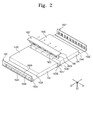
- FIG. 2 is an exploded perspective view showing a coupling relation between the light guide part 150 and first to third light emitting diode packages 162, 162', and 162" of FIG. 1 .
- the light guide part 150 includes a first light guide plate 152 and a second light guide plate 154 spaced apart from the first light guide plate 152.
- Each of the first, second, and third light emitting diode packages 162, 162', and 162" is disposed adjacent to at least one side of the first and second light guide plates 152 and 154.
- first and second light guide plates 152 and 154 have a plate-like shape.
- the first light guide plate 152 includes a first light incident surface 152A and a second light incident surface 152B facing the first light incident surface 152A.
- the light guide plate 152 includes a first light exiting surface 152C that connects the first and second light incident surfaces 152A and 152B.
- the first light emitting diode package 162 is positioned to face the first light incident surface 152A.
- the first light emitting diode package 162 extends along a lengthwise direction (hereinafter, referred to as a first direction D1) of the first light incident surface 152A.
- the second light guide plate 154 includes a third light incident surface 154A and a fourth light incident surface 154B facing the third light incident surface 154A.
- the second light guide plate 154 includes a second light exiting surface 154C that connects the third and fourth light incident surfaces 154A and 154B.
- the second light emitting diode package 162' is disposed between the first light guide plate 152 and the second light guide plate 154 such that each surface thereof faces the second light incident surface 152B and the fourth light incident surface 154B, respectively.
- the second light emitting diode package 162' extends along the first direction D1.
- the third light emitting diode package 162" is disposed to face the third light incident surface 154A.
- the third light emitting diode package 162" extends along a lengthwise direction (e.g., the first direction D1) of the third light incident surface 154A.
- first light emitting diode package 162 and the third light emitting diode package 162" will be explained, and then the second light emitting diode package 162' will be explained.
- FIG. 3 is a perspective view showing a first light emitting diode package of FIG. 2
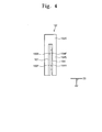
- FIG. 4 is a sectional view taken along a line I-I' of FIG. 3 .
- the first light emitting diode package 162 and the third light emitting diode package 162" have the same structure and function and are symmetrical with each other with reference to the space between the first and second light guide plates 152 and 154. Accordingly, for the convenience of explanation, the first light emitting diode package 162 will be primarily described, and detailed description of the same portion of the third light emitting diode package 162" as the first light emitting diode package 162 will be omitted.
- the first light emitting diode package 162 includes a plurality of light emitting diode chips 162C and a supporting member that holds the light emitting diode chips 162C.
- the supporting member extends in the first direction D1 and includes a frame 162A, a plurality of branches 162B, and a plurality of frame electrodes 166.
- the frame 162A extends in the first direction D1.
- the first direction D1 coincides with the lengthwise direction of the first light incident surface 152A of the first light guide plate 152 and the light emitting diode chips 162C are arranged in the first direction D 1.
- the branches 162B are protruded from the frame 162A in a second direction D2 substantially perpendicular to the first direction D1.
- Two branches 162B adjacent to each other are spaced apart from each other with a space interposed therebetween to receive one of the light emitting diode chips 162C.
- at least three branches 162B are provided to receive at least two light emitting diode chips 162C in a line.
- the light emitting diode chips 162C may be coupled with the branches 162B using various structures, such as a concavo-convex coupling structure, a hook-type coupling structure, a clip-type coupling structure, etc.
- a concavo-convex coupling structure will be described as a representative example, but coupling structures in other embodiments of the invention are not limited thereto.
- Each branch 162B is provided with a guide recess 167 formed by recessing a surface facing a surface of an adjacent branch.
- the guide recess 167 is recessed toward the first direction D1 from the surface thereof.
- the guide recess 167 extends in the second direction D2 to have a rectangular cavity shape.
- the frame 162A and the branches 162B include an insulative material such as a polymer resin, such as an acryl resin, an epoxy resin, etc.
- the frame 162A and the branches 162B may be integrally formed with each other.
- the frame 162A and the branches 162B may be formed through a single process, such as a molding process, by using the same material.
- the frame 162A and the branches 162B may be formed of a material that diffuses the light emitted from the light emitting diode chips 162C.
- the frame electrodes 166 are located inside the guide recesses 167 in a one-to-one correspondence.
- Each of the frame electrodes 166 has a plate-like shape including a front surface and a rear surface and is thinner than a width of the guide recess 167.
- the frame electrode 166 is fixed inside the guide recess 167 such that the rear surface of each frame electrode 166 is parallel to a surface of the frame 162A.
- the front surface of each of the frame electrodes 166 may be spaced apart from the inner surface of each of the guide recesses 167 facing the front surface of the frame electrode 166.
- Each of the frame electrodes 166 is provided with at least one of a protrusion 166P and a recess 166R, which are formed on the front surface of the frame electrodes 166.
- the protrusion 166P and the recess 166R are used to fix the light emitting diode chips 162C to the supporting member.
- representative frame electrodes 166 each provided with one protrusion 166P and one recess 166R shape have been shown in FIGS. 3 and 4 as having a hemispherical shape, but the number and shape of the protrusions and recesses in other embodiments of the invention is not limited thereto. That is, a plurality of protrusions 166P or the recesses 166R may be provided having various other shapes, such as a polypyramid shape, a polyhedron shape, a hook shape, etc.
- the frame electrodes 166 include a conductive material since they are used to apply a power source voltage to the light emitting source chips 162C.
- Each of the light emitting diode chips 162C includes a body part and a wing part 164.
- the body part includes a supporter 165 and a light emitting diode 163.
- the supporter 165 has a plate-like shape having a front surface and a rear surface.
- the supporter 165 may include a polymer insulating material such as an epoxy resin, acryl resin, but is not limited thereto.
- a width of the supporter 165 of each light emitting diode chip 162C in the first direction is narrower than a width of the supporter 165 in the second direction.
- the light emitting diode 163 emits the light and is mounted on the front surface of the supporter 165.
- the light emitting diode 163 emits light that propagates away from the front surface of the supporter 165.
- the wing part 164 protrudes from both sides of the supporter 165 of each of the light emitting diode chips 162C. That is, a pair of wing parts 164 is provided to each supporter 165 of each of the light emitting diode chips 162C.
- the wing part 164 corresponds to the guide recess 167 and extends along the second direction D2.
- the wing part 164 is provided with at least one of a protrusion 164P and a recess 164R.
- the protrusion 164P and the recess 164R of each wing part 164 correspond to the recess 166R and the protrusion 166P of the frame electrodes 166 in number, position, and structure.
- the wing part 164 is formed of a conductive material such that each wing part 164 is electrically connected to the corresponding frame electrode 166 when inserted into the corresponding guide recess 167.
- the light emitting diode chip 162C is positioned such that a light exiting surface of the light emitting diode chip 162C is parallel to the surface of the frame 162A. Then, end portions of the wing parts 164 are respectively inserted into the guide recesses 167 of the two adjacent branches 162B, and then the light emitting diode chip 162C is pressed such that the light emitting diode chip 162C moves to the frame 162A from a lower portion of the branches 162B.
- Each wing part 164 is provided with at least one of the protrusion 164P and the recess 164R and each frame electrode 166 is provided with at least one of the protrusion 166P and the recess 166R.
- the protrusion 164P of the wing part 164 is engaged with the recess 166R of the frame electrode 166 and the recess 164R of the wing part 164 is engaged with the protrusion 166P of the frame electrode 166.
- the light emitting diode chip 162C is completely coupled with the supporting member.
- each of the light emitting diode chips 162C may be inserted between corresponding adjacent branches 162B in a line.
- the number of the light emitting diode chips 162C may be adjusted according to the number of the branches 162B.
- a printed circuit board 162p may be provided below the first light emitting diode package 162 to make contact with the lower portion of the branches 162B.
- the printed circuit board 162p supports the first light emitting diode package 162 and applies the power source voltage to the first light emitting diode package 162.
- the printed circuit board 162p has an upper surface and a lower surface and extends in the first direction to have an elongated shape. Although not shown in FIGS. 1 to 4 , the printed circuit board 162p may include a wire connected to an external power source. The printed circuit board 162p is arranged such that the upper surface thereof is positioned perpendicular to the direction D2. The wire is connected to a wire 169 in the first light emitting diode package 162, shown in FIG. 5 and described below, to apply the power source voltage to the light emitting diode chips 162C.
- the upper surface of the printed circuit board 162p makes contact with the supporting member.
- the upper surface may make contact with the lower portion of the branches 162B or a lower portion of the frame 162A.
- the branches 162B are positioned lower than the frame 162A and the frame 162A is positioned higher than the branches 162B.
- each of the light emitting diode chips 162C is inserted upwardly between the corresponding adjacent branches 162B.
- the printed circuit board 162p making contact with the lower portion of the branches 162B will be described as a representative, non-limiting example.
- the branches 162B are positioned higher than the frame 162A and the frame 162A is positioned lower than the branches 162B.
- the light emitting diode chips 162C may be coupled with the supporting member after the printed circuit board 162p makes contact with the supporting member.
- a method of contacting the printed circuit board 162p with the first light emitting diode package 162 is not limited thereto. That is, the first light emitting diode package 162 may be fixed to the printed circuit board 162p after coating an adhesive (not shown) on the first light emitting diode package 162 or the printed circuit board 162p. In addition, although not shown in figures, the first light emitting diode package 162 may be coupled with the printed circuit board 162p using other methods, such as a screw coupling structure, a hook coupling structure, a concavo-convex coupling structure, etc.
- the reference numerals 162p' and 162p" denote printed circuit boards respectively coupled with the second light emitting diode package 162' and the third light emitting diode package 162".
- the coupling method and structure between the printed circuit board 162p'and the second light emitting diode package 162', and between the printed circuit board 162p"and the third light emitting diode package 162" is substantially the same as that between the printed circuit board 162p and the first light emitting diode package 162, and thus detailed descriptions thereof will be omitted.
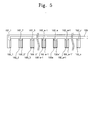
- FIG. 5 is a sectional view taken along a line II-II' of FIG. 3 .
- the supporting member includes the branches 162B.
- the branches 162B includes a first branch 162_1 to n-th branch 162_n (n is a natural number equal to or larger than 3).
- Each frame electrode 166 is disposed inside the corresponding guide recess of the first to n-th branches 162_1 to 162_n.
- the frame electrodes 166 includes first frame electrodes 166_1 and 166_n, second frame electrodes 166_2 to 166_n-1, and third frame electrodes 166_2' to 166_n-1'.
- the first frame electrodes include the frame electrode 166_1 coupled with the first branch 162_1 and the frame electrode 166_n coupled with the n-th branch 162_n.
- the first branch 162_1 and the n-th branch 162_n correspond to outermost branches among the first to n-th branches 162_1 to 162_n.
- the second frame electrodes include the frame electrodes 166_2 to 166_n-1 each positioned at a first side portion of each corresponding branch 166_2 to 162_n-1
- the third frame electrodes include the frame electrodes 166_2' to 166_n-1' each positioned at a second side portion of each corresponding branch 166_2 to 162_n-1.
- the first branch 162_1 includes the first frame electrode 166_1 disposed at the second side portion thereof facing the first side of the second branch 162_2.
- the second branch 162_2 includes the second frame electrode 166_2 disposed at the first side portion thereof facing the second side portion of the first branch 162_1 and the third frame electrode 166_2' disposed at the second side portion thereof facing the third branch 162_3.
- an m-th branch 162_m (m is a natural number larger than 1 and smaller than n) includes the second frame electrode 166_m-1 disposed at the first side portion thereof facing an (m-1)-th branch 162_m-1 and the third frame electrode 166_m' disposed at the second side portion thereof facing an (m+1)-th branch 162_m+1.
- an n-th branch 162_n includes the first frame electrode (not shown) disposed at the first side portion thereof facing an (n-1)-th branch.
- the first frame electrode 166-1 and the n-th frame electrode 166_n are connected to the printed circuit board 162p through the wires 169.
- the second and third frame electrodes included in each branch are connected to each other via the wires (169).
- the second frame electrode 166-m in the m-th branch 162_m is connected to the third frame electrode 166_m' in the m-th branch 162_m via the wires 169.
- the second frame electrodes 166_2 to 166_n and the third frame electrode 166_2' to 166_n-1' are electrically insulated from the external power source since the first frame electrodes 166_1 and 166_n are electrically connected to the external power source.
- the frame electrodes 166 respectively disposed at two adjacent branches 162B are electrically connected to each other through the corresponding light emitting diode chip 162 inserted between the adjacent branches 162B.
- the third frame electrode 166_m-1' of the (m-1)-th branch 162_m-1 is electrically connected to the second frame electrode 166_m of the m-th branch 162_m through the light emitting diode chip 162C inserted between the (m-1)-th branch 162_m-1 and the m-th branch 162_m.
- the first frame electrodes 166_1 and 166_n are connected to the external power source after inserting the light emitting diode chips 163C between the branches 162B, the first frame electrodes 166_1 and 166_n, the second frame electrodes 166_2 to 166_n-1, the third frame electrodes 166_2' to 166_n-1', and the light emitting diode chips 162C are connected to each other in series.
- the first light emitting diode package 162 may be electrically connected to the printed circuit board 162p.
- the light emitting diode chips 162C are not required to be directly connected to the printed circuit board 162p and it is enough that the first frame electrodes 166_1 and 166_n are electrically connected to the printed circuit board 162p.
- the first light emitting diode package 162 to which the external power source voltage is applied emits light in a direction, such as the third direction D3, substantially perpendicular to the first and second directions D1 and D2.
- FIG. 6 is a perspective view showing the second light emitting diode package of FIG. 2
- FIG. 7 is a sectional view taken along a line III-III' of FIG. 6 .
- the same reference numerals denote the same elements in FIG. 3 , and thus detailed descriptions of the same elements will be omitted.
- the second light emitting diode package 162' includes the light emitting diode chips 162C and the supporting member that holds the light emitting diode chips 162C.
- the supporting member includes the frame 162A, the branches 162B, and the frame electrodes 166.
- the frame 162A extends in the first direction D1.
- the branches 162B are protruded in the second direction D2 substantially perpendicular to the first direction D1 from the frame 162A. Adjacent branches 162B are spaced apart from each other to provide a space therebetween in which one of the light emitting diode chips 162C is accommodated. According to an embodiment of the invention, at least three branches 162B are provided to arrange at least two light emitting diode chips 162C.
- Each branch 162B is provided with the guide recess 167 formed by recessing the surface facing the surface of the adjacent branch. The guide recess 167 is recessed toward the first direction D1 from the surface thereof.
- Each of the light emitting diode chips 162C is inserted between the adjacent branches 162B.
- Each of the light emitting diode chips 162C includes the body part and the wing part 164, and the body part includes the supporter 165 and the light emitting diode 163.
- the supporter 165 has the plate-like shape having the front surface and the rear surface.
- the wing part 164 protrudes from both sides of the supporter 165 of each of the light emitting diode chips 162C. That is, a pair of wing parts 164 is provided to each supporter 165 of each of the light emitting diode chips 162C.
- the wing parts 164 of each of the light emitting diode chips 162C are respectively inserted into the guide recesses 167 when each of the light emitting diode chips 162C is inserted between the corresponding adjacent branches 162B.
- the light emitting diode chips 162C are positioned such that light exiting surfaces of the light emitting diodes 163 are parallel to the surface of the frame 162A.
- the light emitting diode chips 162C are arranged such that the light exiting surfaces of the light emitting diodes 163 face the same direction, but, for the second light emitting diode package 162', the light emitting diode chips 162C are arranged such that the light exiting surfaces of the light emitting diode chips 162C alternately face opposite directions.
- the light emitting diodes 163 may emit light propagating in opposite directions substantially perpendicular to both surfaces of the frame 162A. Accordingly, the second light emitting diode package 162' may provide light to the second light incident surface 152B and the fourth light incident surface 154B.
- the light exiting surfaces of the light emitting diodes 163 are arranged to alternately face opposite directions, but other embodiments of the invention are not limited thereto.
- the supporting member is divided into plural areas, the light exiting surfaces of the light emitting diodes 163 in different areas may be arranged to alternately face opposite directions. That is, the light exiting surfaces of the light emitting diodes 163 included in the same area face the same direction, and the light exiting surfaces of the light emitting diodes 163 included in adjacent areas face the opposite direction.
- the propagation direction and intensity of the light may be controlled.
- the frame 162A of the second light emitting diode package 162' is provided with a cover 168 that extends from both sides of an upper portion of the frame 162A in directions substantially perpendicular to the first and second directions D1 and D2.
- the cover 168 has a plate-like shape and extends in the first direction D1.
- the cover 168 covers a portion of the first light guide plate 152 and a portion of the light guide plate 154, which face each other. Consequently, an upper portion of the second light incident surface 152B and an upper portion of the fourth light incident surface 154B are covered by the cover 168.
- the light emitted from the second light emitting diode package 162' is incident to the second and fourth light incident surfaces 152B and 154B and provided to the display panel 120 through the first and second light exiting surfaces 152C and 154C, respectively.
- the first light guide plate 152 and the second light guide plate 154 are spaced apart from each other by the second light emitting diode package 162', the light emitted from the light emitting diode chips 162C may propagate upward through the space between the first and second light guide plates 152 and 154, rather than being incident to the second light incident surface 152B or the fourth light incident surface 154B.
- the cover 168 may block or diffuse the light propagating upwards.
- the cover 168 may include an opaque material (e.g., a black material) to block the light propagating upwards.
- the cover 168 may include a light diffusion material to diffuse the light propagating upwards. Therefore, a bright line caused by the light propagating upwards through the space between the first and second light guide plates 152 and 154 may be prevented, thereby preserving brightness uniformity of the display panel 120.
- the cover 168 may prevent the first and second light guide plates 152 and 154 from coming off.
- the first and second light guide plates 152 and 154 may move upwards or expand due to heat applied from the first, second, and third light emitting diode packages 162, 162', and 162".
- the first and second light guide plates 152 and 154 may shift from their original positions.
- the cover 168 provided with the frame 162A and the branches 162B may hold the positions of the first and second light guide plates 152 and 154.
- the cover 168 includes an insulative material such as polymer resin, such as an acryl resin, an epoxy resin, etc.
- the cover 168 may be integrally formed with the frame 162A and the branches 162B.
- the cover 168, the frame 162A, and the branches 162B may be formed through a single process, such as a molding process, using the same material.
- the light emitting diode chips 162C are securely fixed to the supporting member and the corresponding printed circuit board of the printed circuit boards 162p, 162p', and 162p" and are arranged in line in the first direction D1. Accordingly, the light emitting diode chips 162C may be securely held in place, as opposed to the case when the light emitting diode chips are mounted on a printed circuit board without employing a supporting member.
- conventional light emitting diode chips are vertically and independently mounted on a printed circuit board. It is challenging to vertically mount a thin plate shape light emitting diode chip onto a printed circuit board and the mounted chips are easily inclined by external forces, causing light leakage and display defects on the display panel.
- the light emitting diode chips are inserted into guide recesses formed in the frame 162A, and are arranged in a line with a uniform spacing. Thus, the light emitting diode chips may be securely held in place to prevent light leakage and improve display quality.
- the light emitting diode chip need to be supplied with the power source voltage, in the case when the power source voltage is applied to the wire in the light emitting diode package, not all of the light emitting diode chips need to be directly mounted on the printed circuit board.
- the printed circuit board used to fix the lower portion of the light emitting diode package may be removed.
- the first to third light emitting diode packages 162, 162', and 162" may be mounted on another element, such as the lower cover 180.
- the first to third light emitting diode packages 162, 162', and 162" may be attached onto a mold frame used to receive the optical member 130.
- the first light emitting diode package 162, the second light emitting diode package 162', and the third light emitting diode package 162" may be operated independently, so that different intensities of light may be provided to the first light guide plate 152 and to the second light guide plate 154. Accordingly, the light intensity provided to the display panel 120 through the first light guide plate 152 and the second light guide plate 154 may be adjusted according to the position of the display area of the display panel 120, thereby realizing local dimming.
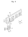
- FIG. 8 is a perspective view showing a first light emitting diode package according to another exemplary embodiment of the present invention.
- a light emitting diode package 262 according to a present exemplary embodiment has the similar structure and function as those of the first light emitting diode package 162 shown in FIG. 3 , and thus the same reference numerals are assigned to the same elements and detailed description of the same elements will be omitted.
- the first light emitting diode package 262 extends in the first direction D1 and includes a back plate 162D that makes contact with a surface of the supporting member and the light emitting diode chips.
- the back plate 162D may be integrally formed with the supporting member.
- the back plate 162D may be formed through a single process, such as a molding process, with the frame 162A and the branches 162B.
- the back plate 162D may include a material that may diffuse light and include a material identical to the material for the supporting member, such as polymer resin (for example, an acryl resin, an epoxy resin, etc.).
- polymer resin for example, an acryl resin, an epoxy resin, etc.
- the structure of the back plate 162D is not limited thereto in other embodiments of the invention.
- the back plate 162D may be attached to the surface of the supporting member after being separately formed.
- the back plate 162D attached to or integrally formed with the supporting member may enhance the strength of the supporting member, so the supporting member may maintain its original shape. In other words, the back plate 162D may prevent the frame 162A and the branches 162B from being bent or damaged, thereby securely holding the light emitting diode chips 162C.
- the number of the light guide plates and the number of the light emitting diode packages may vary.
- the first light emitting diode package may be disposed adjacent to at least one side of the light guide plate to provide light to the light guide plate.
- the second light emitting diode package may be disposed in a cross shape between the four light guide plates.
Landscapes
- Physics & Mathematics (AREA)
- General Physics & Mathematics (AREA)
- Optics & Photonics (AREA)
- Nonlinear Science (AREA)
- Mathematical Physics (AREA)
- Chemical & Material Sciences (AREA)
- Crystallography & Structural Chemistry (AREA)
- Engineering & Computer Science (AREA)
- Microelectronics & Electronic Packaging (AREA)
- Planar Illumination Modules (AREA)
- Led Device Packages (AREA)
Abstract
Description
- This application claims priority under 35 U.S.C. § 119 from Korean Patent Application No.
2010-44107 filed on May 11, 2010 - Embodiments of the present invention are directed to a light emitting diode package and a display apparatus having the light emitting diode package.
- In general, a display apparatus such as a liquid crystal display or an electrophoresis display includes a liquid crystal display panel or an electrophoresis display panel to display an image. However, the liquid crystal display panel and the electrophoresis display panel are not self-emissive, so the display apparatus requires a backlight assembly to provide light to the display panels.
- A display apparatus that can be driven by a local dimming method has been developed to reduce power consumption in the backlight assembly and improve the contrast ratio in the display panel. According to the local dimming method, the amount of light provided to the display panel changes depending upon the image displayed on the display panel.
- Exemplary embodiments of the present invention provide a light emitting diode package capable of improving its assemblability.
- Exemplary embodiments of the present invention provide a display apparatus having the light emitting diode package.
- According to an embodiment of the invention, a light emitting apparatus includes at least one light emitting diode package, a printed circuit board, and at least one light guide plate.
- The light emitting diode package provides light. The light emitting diode package includes a supporting member extending in a first direction and a plurality of light emitting diode chips to provide light. The light emitting diode chips are inserted into the supporting member in a second direction perpendicular to the first direction to be parallel to a surface of the supporting member.
- The supporting member includes a frame and a plurality of branches. The frame extends in the first direction. The branches are branched from the frame in the second direction and spaced apart from each other. Each of the light emitting diode chips is inserted between and coupled with two adjacent branches and has a light exiting surface substantially parallel to the surface of the frame.
- The light emitting diode package further comprises a back plate extending in the first direction and making contact with the surface of the supporting member and the light emitting diode chips.
- The printed circuit board is arranged perpendicular to the second direction to contact the supporting member and supply a power source voltage to the light emitting diode package. The printed circuit board may make contact either the frame or the supporting member.
- The light guide plate may be disposed between a display panel and the light emitting diode package to guide the light to the display panel.
- According to the above, since the light emitting diode chips are fixed to the supporting member in a line, the light emitting diode chips may be securely held in place, thereby preventing the occurrence of a bright line phenomenon. In addition, the light emitting diode package includes a frame electrode connected to a power source, so a process for providing an electrical connection between the light emitting diodes and the printed circuit board may be omitted.
-
-
FIG. 1 is an exploded perspective view showing a display apparatus according to an exemplary embodiment of the present invention. -
FIG. 2 is an exploded perspective view showing a coupling relation between a light guide part and first to third light emitting diode packages ofFIG. 1 . -
FIG. 3 is a perspective view showing a first light emitting diode package ofFIG. 2 . -
FIG. 4 is a sectional view taken along a line I-I' ofFIG. 3 . -
FIG. 5 is a sectional view taken along a line II-II' ofFIG. 3 . -
FIG. 6 is a perspective view showing a second light emitting diode package ofFIG. 2 . -
FIG. 7 is a sectional view taken along a line III-III' ofFIG. 6 . -
FIG. 8 is a perspective view showing a first light emitting diode package according to another exemplary embodiment of the present invention. - It will be understood that when an element or layer is referred to as being "on", "connected to" or "coupled to" another element or layer, it can be directly on, connected or coupled to the other element or layer or intervening elements or layers may be present. Like numbers refer to like elements throughout.
- Hereinafter, exemplary embodiments of the present invention will be explained in detail with reference to the accompanying drawings.
-
FIG. 1 is an exploded perspective view showing a display apparatus according to an exemplary embodiment of the present invention. - Referring to
FIG. 1 , adisplay apparatus 100 includes adisplay panel 120, a backlight assembly BA, alower cover 180, and anupper cover 110. - The
display panel 120 can display an image. Thedisplay panel 120 may be one of various display panels such as a liquid crystal display panel or an electrophoresis display panel. In a present exemplary embodiment, a liquid crystal display panel will be described as a representative example, however, other embodiments of the invention are not limited thereto. - The
display panel 120 has a plate-like shape having a long side and a short side. Thedisplay panel 120 includes afirst substrate 122, a second substrate 124 opposite to thefirst substrate 122, and a liquid crystal layer (not shown) disposed between the first andsecond substrates 122 and 124. - The
first substrate 122 may include a plurality of pixel electrodes (not shown) and a plurality of thin film transistors electrically connected to the pixel electrodes in one-to-one correspondence. Each thin film transistor switches a driving signal applied to its corresponding pixel electrode. In addition, the second substrate 124 may include a common electrode that forms an electric field with the pixel electrodes to control the arrangement of the liquid crystal molecules in the liquid crystal layer. Thus, thedisplay panel 120 may display an image corresponding to the arrangement of the liquid crystal molecules. - The backlight assembly BA is disposed below the
display panel 120. The backlight assembly BA includes alight source part 160, alight guide part 150, anoptical member 130, and areflection sheet 170. - The
light source part 160 provides thedisplay panel 120 with the light used to display the image on thedisplay panel 120. Thelight guide part 150 guides the light provided from thelight source part 160 to thedisplay panel 120. - The
light guide part 150 includes one or more light guide plates. Hereinafter, alight guide part 150 having two light guide pates will be described as a representative example, but the number of the light guide plates in thelight guide part 150 is not limited thereto. The two light guide plates will be referred to as a firstlight guide plate 152 and a secondlight guide plate 154, respectively. - The
light source part 160 includes a first lightemitting diode package 162, a second light emitting diode package 162', and a third lightemitting diode package 162". The first and secondlight guide plates emitting diode package 162, the second light emitting diode package 162', and the third lightemitting diode package 162" to provide the light to thedisplay panel 120. - The
optical member 130 is disposed between thelight guide part 150 and thedisplay panel 120. Theoptical member 130 controls the light output from thelight source part 160. Theoptical member 130 includes adiffusion sheet 136, aprism sheet 134, and aprotection sheet 132, which are sequentially stacked on thelight guide part 150. - The
diffusion sheet 136 diffuses the light output from thelight source part 160. Theprism sheet 134 condenses the light diffused by thediffusion sheet 134 to allow the light to travel in a vertical direction with respect to thedisplay panel 120. The light passing through theprism sheet 134 is vertically incident to thedisplay panel 120. Theprotection sheet 132 is disposed on theprism sheet 134 to protect theprism sheet 134 from external impacts. - In a present exemplary embodiment, the
optical member 130 including thediffusion sheet 136, theprism sheet 134, and theprotection sheet 132 has been shown as a representative example, but it should not be limited thereto. That is, one or more of each of thediffusion sheet 136, theprism sheet 134, and theprotection sheet 132 may be provided, or each may be removed from theoptical member 130. - The
reflection sheet 170 is disposed on thelower cover 180 below thelight source part 160. Thereflection sheet 170 may include a reflective material Thereflection sheet 170 reflects to thedisplay panel 120 light that leaked downward from thelight guide part 160, and light from the first, second, and the third light emitting diode packages 162, 162', and 162". As a result, thereflection sheet 170 may increase an amount of the light traveling to thedisplay panel 120. - The
upper cover 110 is disposed on thedisplay panel 120. Theupper cover 110 is provided with adisplay window 111 formed therethrough to expose a display area of thedisplay panel 120. Thus, theupper cover 110 may support a front end of thedisplay panel 120 when coupled with thelower cover 180. - The
lower cover 180 provides a receiving space in which the backlight assembly BA and thedisplay panel 120 are received. Theupper cover 110 is coupled with thelower cover 180 to fix the backlight assembly BA and thedisplay panel 120 to thelower cover 180. -
FIG. 2 is an exploded perspective view showing a coupling relation between thelight guide part 150 and first to third light emitting diode packages 162, 162', and 162" ofFIG. 1 . - Referring to
FIG. 2 , thelight guide part 150 includes a firstlight guide plate 152 and a secondlight guide plate 154 spaced apart from the firstlight guide plate 152. Each of the first, second, and third light emitting diode packages 162, 162', and 162" is disposed adjacent to at least one side of the first and secondlight guide plates - In particular, the first and second
light guide plates light guide plate 152 includes a firstlight incident surface 152A and a secondlight incident surface 152B facing the firstlight incident surface 152A. In addition, thelight guide plate 152 includes a firstlight exiting surface 152C that connects the first and second light incident surfaces 152A and 152B. - The first light emitting
diode package 162 is positioned to face the firstlight incident surface 152A. The first light emittingdiode package 162 extends along a lengthwise direction (hereinafter, referred to as a first direction D1) of the firstlight incident surface 152A. - The second
light guide plate 154 includes a thirdlight incident surface 154A and a fourthlight incident surface 154B facing the thirdlight incident surface 154A. In addition, the secondlight guide plate 154 includes a secondlight exiting surface 154C that connects the third and fourth light incident surfaces 154A and 154B. - The second light emitting diode package 162' is disposed between the first
light guide plate 152 and the secondlight guide plate 154 such that each surface thereof faces the secondlight incident surface 152B and the fourthlight incident surface 154B, respectively. The second light emitting diode package 162' extends along the first direction D1. - The third light emitting
diode package 162" is disposed to face the thirdlight incident surface 154A. The third light emittingdiode package 162" extends along a lengthwise direction (e.g., the first direction D1) of the thirdlight incident surface 154A. - Hereinafter, the first light emitting
diode package 162 and the third light emittingdiode package 162" will be explained, and then the second light emitting diode package 162' will be explained. -
FIG. 3 is a perspective view showing a first light emitting diode package ofFIG. 2 , andFIG. 4 is a sectional view taken along a line I-I' ofFIG. 3 . - Referring to
FIGS. 1 to 4 , the first light emittingdiode package 162 and the third light emittingdiode package 162" have the same structure and function and are symmetrical with each other with reference to the space between the first and secondlight guide plates diode package 162 will be primarily described, and detailed description of the same portion of the third light emittingdiode package 162" as the first light emittingdiode package 162 will be omitted. - The first light emitting
diode package 162 includes a plurality of light emittingdiode chips 162C and a supporting member that holds the light emittingdiode chips 162C. - The supporting member extends in the first direction D1 and includes a
frame 162A, a plurality ofbranches 162B, and a plurality offrame electrodes 166. - The
frame 162A extends in the first direction D1. The first direction D1 coincides with the lengthwise direction of the firstlight incident surface 152A of the firstlight guide plate 152 and the light emittingdiode chips 162C are arranged in thefirst direction D 1. - The
branches 162B are protruded from theframe 162A in a second direction D2 substantially perpendicular to the first direction D1. Twobranches 162B adjacent to each other are spaced apart from each other with a space interposed therebetween to receive one of the light emittingdiode chips 162C. According to an embodiment of the invention, at least threebranches 162B are provided to receive at least two light emittingdiode chips 162C in a line. The light emittingdiode chips 162C may be coupled with thebranches 162B using various structures, such as a concavo-convex coupling structure, a hook-type coupling structure, a clip-type coupling structure, etc. In a present exemplary embodiment, a concavo-convex coupling structure will be described as a representative example, but coupling structures in other embodiments of the invention are not limited thereto. - Each
branch 162B is provided with aguide recess 167 formed by recessing a surface facing a surface of an adjacent branch. Theguide recess 167 is recessed toward the first direction D1 from the surface thereof. Theguide recess 167 extends in the second direction D2 to have a rectangular cavity shape. - In a present exemplary embodiment, the
frame 162A and thebranches 162B include an insulative material such as a polymer resin, such as an acryl resin, an epoxy resin, etc. In addition, theframe 162A and thebranches 162B may be integrally formed with each other. Theframe 162A and thebranches 162B may be formed through a single process, such as a molding process, by using the same material. Theframe 162A and thebranches 162B may be formed of a material that diffuses the light emitted from the light emittingdiode chips 162C. - The
frame electrodes 166 are located inside the guide recesses 167 in a one-to-one correspondence. Each of theframe electrodes 166 has a plate-like shape including a front surface and a rear surface and is thinner than a width of theguide recess 167. When locating aframe electrode 166 inside aguide recess 167, theframe electrode 166 is fixed inside theguide recess 167 such that the rear surface of eachframe electrode 166 is parallel to a surface of theframe 162A. Thus, the front surface of each of theframe electrodes 166 may be spaced apart from the inner surface of each of the guide recesses 167 facing the front surface of theframe electrode 166. - Each of the
frame electrodes 166 is provided with at least one of aprotrusion 166P and arecess 166R, which are formed on the front surface of theframe electrodes 166. Theprotrusion 166P and therecess 166R are used to fix the light emittingdiode chips 162C to the supporting member. - In a present exemplary embodiment,
representative frame electrodes 166 each provided with oneprotrusion 166P and onerecess 166R shape have been shown inFIGS. 3 and4 as having a hemispherical shape, but the number and shape of the protrusions and recesses in other embodiments of the invention is not limited thereto. That is, a plurality ofprotrusions 166P or therecesses 166R may be provided having various other shapes, such as a polypyramid shape, a polyhedron shape, a hook shape, etc. - The
frame electrodes 166 include a conductive material since they are used to apply a power source voltage to the light emitting source chips 162C. - Each of the light emitting
diode chips 162C includes a body part and awing part 164. - The body part includes a
supporter 165 and alight emitting diode 163. Thesupporter 165 has a plate-like shape having a front surface and a rear surface. Thesupporter 165 may include a polymer insulating material such as an epoxy resin, acryl resin, but is not limited thereto. In a present exemplary embodiment, a width of thesupporter 165 of each light emittingdiode chip 162C in the first direction is narrower than a width of thesupporter 165 in the second direction. - The
light emitting diode 163 emits the light and is mounted on the front surface of thesupporter 165. Thelight emitting diode 163 emits light that propagates away from the front surface of thesupporter 165. - The
wing part 164 protrudes from both sides of thesupporter 165 of each of the light emittingdiode chips 162C. That is, a pair ofwing parts 164 is provided to eachsupporter 165 of each of the light emittingdiode chips 162C. Thewing part 164 corresponds to theguide recess 167 and extends along the second direction D2. - The
wing part 164 is provided with at least one of aprotrusion 164P and arecess 164R. Theprotrusion 164P and therecess 164R of eachwing part 164 correspond to therecess 166R and theprotrusion 166P of theframe electrodes 166 in number, position, and structure. Thewing part 164 is formed of a conductive material such that eachwing part 164 is electrically connected to thecorresponding frame electrode 166 when inserted into thecorresponding guide recess 167. - Hereinafter, the coupling structure between the supporting member of the first light emitting
diode package 162 and the light emittingdiode chips 162C will be described in detail. - The light emitting
diode chip 162C is positioned such that a light exiting surface of the light emittingdiode chip 162C is parallel to the surface of theframe 162A. Then, end portions of thewing parts 164 are respectively inserted into the guide recesses 167 of the twoadjacent branches 162B, and then the light emittingdiode chip 162C is pressed such that the light emittingdiode chip 162C moves to theframe 162A from a lower portion of thebranches 162B. Eachwing part 164 is provided with at least one of theprotrusion 164P and therecess 164R and eachframe electrode 166 is provided with at least one of theprotrusion 166P and therecess 166R. Accordingly, when thewing part 164 is inserted into thecorresponding guide recess 167, theprotrusion 164P of thewing part 164 is engaged with therecess 166R of theframe electrode 166 and therecess 164R of thewing part 164 is engaged with theprotrusion 166P of theframe electrode 166. As a result, the light emittingdiode chip 162C is completely coupled with the supporting member. - As described above, each of the light emitting
diode chips 162C may be inserted between correspondingadjacent branches 162B in a line. The number of the light emittingdiode chips 162C may be adjusted according to the number of thebranches 162B. - According to a present exemplary embodiment, a printed
circuit board 162p may be provided below the first light emittingdiode package 162 to make contact with the lower portion of thebranches 162B. The printedcircuit board 162p supports the first light emittingdiode package 162 and applies the power source voltage to the first light emittingdiode package 162. - The printed
circuit board 162p has an upper surface and a lower surface and extends in the first direction to have an elongated shape. Although not shown inFIGS. 1 to 4 , the printedcircuit board 162p may include a wire connected to an external power source. The printedcircuit board 162p is arranged such that the upper surface thereof is positioned perpendicular to the direction D2. The wire is connected to awire 169 in the first light emittingdiode package 162, shown inFIG. 5 and described below, to apply the power source voltage to the light emittingdiode chips 162C. - The upper surface of the printed
circuit board 162p makes contact with the supporting member. The upper surface may make contact with the lower portion of thebranches 162B or a lower portion of theframe 162A. In particular, in the case in which the upper surface of the printedcircuit board 162p makes contact with the lower portion of thebranches 162B, as shown inFIGS. 2 and3 , thebranches 162B are positioned lower than theframe 162A and theframe 162A is positioned higher than thebranches 162B. In this case, each of the light emittingdiode chips 162C is inserted upwardly between the correspondingadjacent branches 162B. In a present exemplary embodiment, the printedcircuit board 162p making contact with the lower portion of thebranches 162B will be described as a representative, non-limiting example. - Alternatively, although not shown in
FIGS. 1 to 4 , in the case in which the upper surface of the printedcircuit board 162p makes contact with the lower portion of theframe 162A, thebranches 162B are positioned higher than theframe 162A and theframe 162A is positioned lower than thebranches 162B. In this case, since each of the light emittingdiode chips 162C is inserted downwardly between the correspondingadjacent branches 162B, the light emittingdiode chips 162C may be coupled with the supporting member after the printedcircuit board 162p makes contact with the supporting member. - A method of contacting the printed
circuit board 162p with the first light emittingdiode package 162 is not limited thereto. That is, the first light emittingdiode package 162 may be fixed to the printedcircuit board 162p after coating an adhesive (not shown) on the first light emittingdiode package 162 or the printedcircuit board 162p. In addition, although not shown in figures, the first light emittingdiode package 162 may be coupled with the printedcircuit board 162p using other methods, such as a screw coupling structure, a hook coupling structure, a concavo-convex coupling structure, etc. - In
FIG. 2 , thereference numerals 162p' and 162p" denote printed circuit boards respectively coupled with the second light emitting diode package 162' and the third light emittingdiode package 162". The coupling method and structure between the printed circuit board 162p'and the second light emitting diode package 162', and between the printedcircuit board 162p"and the third light emittingdiode package 162", is substantially the same as that between the printedcircuit board 162p and the first light emittingdiode package 162, and thus detailed descriptions thereof will be omitted. -
FIG. 5 is a sectional view taken along a line II-II' ofFIG. 3 . - Referring to
FIGS. 3 to 5 , the supporting member includes thebranches 162B. - The
branches 162B includes a first branch 162_1 to n-th branch 162_n (n is a natural number equal to or larger than 3). Eachframe electrode 166 is disposed inside the corresponding guide recess of the first to n-th branches 162_1 to 162_n. - The
frame electrodes 166 includes first frame electrodes 166_1 and 166_n, second frame electrodes 166_2 to 166_n-1, and third frame electrodes 166_2' to 166_n-1'. - The first frame electrodes include the frame electrode 166_1 coupled with the first branch 162_1 and the frame electrode 166_n coupled with the n-th branch 162_n. The first branch 162_1 and the n-th branch 162_n correspond to outermost branches among the first to n-th branches 162_1 to 162_n. The second frame electrodes include the frame electrodes 166_2 to 166_n-1 each positioned at a first side portion of each corresponding branch 166_2 to 162_n-1, and the third frame electrodes include the frame electrodes 166_2' to 166_n-1' each positioned at a second side portion of each corresponding branch 166_2 to 162_n-1.
- In detail, the first branch 162_1 includes the first frame electrode 166_1 disposed at the second side portion thereof facing the first side of the second branch 162_2. The second branch 162_2 includes the second frame electrode 166_2 disposed at the first side portion thereof facing the second side portion of the first branch 162_1 and the third frame electrode 166_2' disposed at the second side portion thereof facing the third branch 162_3. Similarly, an m-th branch 162_m (m is a natural number larger than 1 and smaller than n) includes the second frame electrode 166_m-1 disposed at the first side portion thereof facing an (m-1)-th branch 162_m-1 and the third frame electrode 166_m' disposed at the second side portion thereof facing an (m+1)-th
branch 162_m+ 1. In addition, an n-th branch 162_n includes the first frame electrode (not shown) disposed at the first side portion thereof facing an (n-1)-th branch. - The first frame electrode 166-1 and the n-th frame electrode 166_n are connected to the printed
circuit board 162p through thewires 169. The second and third frame electrodes included in each branch are connected to each other via the wires (169). For example, the second frame electrode 166-m in the m-th branch 162_m is connected to the third frame electrode 166_m' in the m-th branch 162_m via thewires 169. - Before the light emitting
diode chips 162C are coupled with the supporting member, the second frame electrodes 166_2 to 166_n and the third frame electrode 166_2' to 166_n-1' are electrically insulated from the external power source since the first frame electrodes 166_1 and 166_n are electrically connected to the external power source. - When the light emitting
diode chips 162C are completely coupled with the supporting member, theframe electrodes 166 respectively disposed at twoadjacent branches 162B are electrically connected to each other through the corresponding light emittingdiode chip 162 inserted between theadjacent branches 162B. For example, the third frame electrode 166_m-1' of the (m-1)-th branch 162_m-1 is electrically connected to the second frame electrode 166_m of the m-th branch 162_m through the light emittingdiode chip 162C inserted between the (m-1)-th branch 162_m-1 and the m-th branch 162_m. - As a result, when the first frame electrodes 166_1 and 166_n are connected to the external power source after inserting the light emitting diode chips 163C between the
branches 162B, the first frame electrodes 166_1 and 166_n, the second frame electrodes 166_2 to 166_n-1, the third frame electrodes 166_2' to 166_n-1', and the light emittingdiode chips 162C are connected to each other in series. - As described above, the first light emitting
diode package 162 may be electrically connected to the printedcircuit board 162p. In this case, the light emittingdiode chips 162C are not required to be directly connected to the printedcircuit board 162p and it is enough that the first frame electrodes 166_1 and 166_n are electrically connected to the printedcircuit board 162p. - Consequently, the first light emitting
diode package 162 to which the external power source voltage is applied emits light in a direction, such as the third direction D3, substantially perpendicular to the first and second directions D1 and D2. -
FIG. 6 is a perspective view showing the second light emitting diode package ofFIG. 2 , andFIG. 7 is a sectional view taken along a line III-III' ofFIG. 6 . InFIG. 6 , the same reference numerals denote the same elements inFIG. 3 , and thus detailed descriptions of the same elements will be omitted. - Referring to
FIGS. 1 ,2 ,6 , and7 , the second light emitting diode package 162' includes the light emittingdiode chips 162C and the supporting member that holds the light emittingdiode chips 162C. The supporting member includes theframe 162A, thebranches 162B, and theframe electrodes 166. - The
frame 162A extends in the first direction D1. - The
branches 162B are protruded in the second direction D2 substantially perpendicular to the first direction D1 from theframe 162A.Adjacent branches 162B are spaced apart from each other to provide a space therebetween in which one of the light emittingdiode chips 162C is accommodated. According to an embodiment of the invention, at least threebranches 162B are provided to arrange at least two light emittingdiode chips 162C. Eachbranch 162B is provided with theguide recess 167 formed by recessing the surface facing the surface of the adjacent branch. Theguide recess 167 is recessed toward the first direction D1 from the surface thereof. - Each of the light emitting
diode chips 162C is inserted between theadjacent branches 162B. Each of the light emittingdiode chips 162C includes the body part and thewing part 164, and the body part includes thesupporter 165 and thelight emitting diode 163. - The
supporter 165 has the plate-like shape having the front surface and the rear surface. Thewing part 164 protrudes from both sides of thesupporter 165 of each of the light emittingdiode chips 162C. That is, a pair ofwing parts 164 is provided to eachsupporter 165 of each of the light emittingdiode chips 162C. Thewing parts 164 of each of the light emittingdiode chips 162C are respectively inserted into the guide recesses 167 when each of the light emittingdiode chips 162C is inserted between the correspondingadjacent branches 162B. - The light emitting
diode chips 162C are positioned such that light exiting surfaces of thelight emitting diodes 163 are parallel to the surface of theframe 162A. For the first light emittingdiode package 162, the light emittingdiode chips 162C are arranged such that the light exiting surfaces of thelight emitting diodes 163 face the same direction, but, for the second light emitting diode package 162', the light emittingdiode chips 162C are arranged such that the light exiting surfaces of the light emittingdiode chips 162C alternately face opposite directions. - Since the light exiting surfaces of the
light emitting diodes 163 are arranged to alternately face the opposite directions with respect to the surface of theframe 162A in the second light emitting diode package 162', thelight emitting diodes 163 may emit light propagating in opposite directions substantially perpendicular to both surfaces of theframe 162A. Accordingly, the second light emitting diode package 162' may provide light to the secondlight incident surface 152B and the fourthlight incident surface 154B. - In a present exemplary embodiment, the light exiting surfaces of the
light emitting diodes 163 are arranged to alternately face opposite directions, but other embodiments of the invention are not limited thereto. For example, if the supporting member is divided into plural areas, the light exiting surfaces of thelight emitting diodes 163 in different areas may be arranged to alternately face opposite directions. That is, the light exiting surfaces of thelight emitting diodes 163 included in the same area face the same direction, and the light exiting surfaces of thelight emitting diodes 163 included in adjacent areas face the opposite direction. Thus, the propagation direction and intensity of the light may be controlled. - The
frame 162A of the second light emitting diode package 162' is provided with acover 168 that extends from both sides of an upper portion of theframe 162A in directions substantially perpendicular to the first and second directions D1 and D2. Thecover 168 has a plate-like shape and extends in the first direction D1. - The
cover 168 covers a portion of the firstlight guide plate 152 and a portion of thelight guide plate 154, which face each other. Consequently, an upper portion of the secondlight incident surface 152B and an upper portion of the fourthlight incident surface 154B are covered by thecover 168. - The light emitted from the second light emitting diode package 162' is incident to the second and fourth light incident surfaces 152B and 154B and provided to the
display panel 120 through the first and secondlight exiting surfaces light guide plate 152 and the secondlight guide plate 154 are spaced apart from each other by the second light emitting diode package 162', the light emitted from the light emittingdiode chips 162C may propagate upward through the space between the first and secondlight guide plates light incident surface 152B or the fourthlight incident surface 154B. However, thecover 168 may block or diffuse the light propagating upwards. To this end, thecover 168 may include an opaque material (e.g., a black material) to block the light propagating upwards. In addition, thecover 168 may include a light diffusion material to diffuse the light propagating upwards. Therefore, a bright line caused by the light propagating upwards through the space between the first and secondlight guide plates display panel 120. - In addition, the
cover 168 may prevent the first and secondlight guide plates cover 168, the first and secondlight guide plates light guide plates cover 168 provided with theframe 162A and thebranches 162B may hold the positions of the first and secondlight guide plates - According to a present exemplary embodiment, the
cover 168 includes an insulative material such as polymer resin, such as an acryl resin, an epoxy resin, etc. In addition, thecover 168 may be integrally formed with theframe 162A and thebranches 162B. Thecover 168, theframe 162A, and thebranches 162B may be formed through a single process, such as a molding process, using the same material. - In the first light emitting
diode package 162, the second light emitting diode package 162', and the third light emittingdiode package 162", the light emittingdiode chips 162C are securely fixed to the supporting member and the corresponding printed circuit board of the printedcircuit boards diode chips 162C may be securely held in place, as opposed to the case when the light emitting diode chips are mounted on a printed circuit board without employing a supporting member. - In detail, conventional light emitting diode chips are vertically and independently mounted on a printed circuit board. It is challenging to vertically mount a thin plate shape light emitting diode chip onto a printed circuit board and the mounted chips are easily inclined by external forces, causing light leakage and display defects on the display panel. In a present exemplary embodiment, the light emitting diode chips are inserted into guide recesses formed in the
frame 162A, and are arranged in a line with a uniform spacing. Thus, the light emitting diode chips may be securely held in place to prevent light leakage and improve display quality. - In addition, since not all of the light emitting diode chip need to be supplied with the power source voltage, in the case when the power source voltage is applied to the wire in the light emitting diode package, not all of the light emitting diode chips need to be directly mounted on the printed circuit board. Furthermore, the printed circuit board used to fix the lower portion of the light emitting diode package may be removed. When removing the printed circuit board, the first to third light emitting diode packages 162, 162', and 162" may be mounted on another element, such as the
lower cover 180. In addition, although not shown inFIG. 1 , the first to third light emitting diode packages 162, 162', and 162" may be attached onto a mold frame used to receive theoptical member 130. - Alternatively, the first light emitting
diode package 162, the second light emitting diode package 162', and the third light emittingdiode package 162" may be operated independently, so that different intensities of light may be provided to the firstlight guide plate 152 and to the secondlight guide plate 154. Accordingly, the light intensity provided to thedisplay panel 120 through the firstlight guide plate 152 and the secondlight guide plate 154 may be adjusted according to the position of the display area of thedisplay panel 120, thereby realizing local dimming. -
FIG. 8 is a perspective view showing a first light emitting diode package according to another exemplary embodiment of the present invention. InFIG. 8 , a light emittingdiode package 262 according to a present exemplary embodiment has the similar structure and function as those of the first light emittingdiode package 162 shown inFIG. 3 , and thus the same reference numerals are assigned to the same elements and detailed description of the same elements will be omitted. - The first light emitting
diode package 262 extends in the first direction D1 and includes aback plate 162D that makes contact with a surface of the supporting member and the light emitting diode chips. - The
back plate 162D may be integrally formed with the supporting member. Theback plate 162D may be formed through a single process, such as a molding process, with theframe 162A and thebranches 162B. Theback plate 162D may include a material that may diffuse light and include a material identical to the material for the supporting member, such as polymer resin (for example, an acryl resin, an epoxy resin, etc.). However, the structure of theback plate 162D is not limited thereto in other embodiments of the invention. For example, theback plate 162D may be attached to the surface of the supporting member after being separately formed. - The
back plate 162D attached to or integrally formed with the supporting member may enhance the strength of the supporting member, so the supporting member may maintain its original shape. In other words, theback plate 162D may prevent theframe 162A and thebranches 162B from being bent or damaged, thereby securely holding the light emittingdiode chips 162C. - In the above-described embodiments, two light guide plates and three light emitting diode packages have been described, but the number of the light guide plates and the number of the light emitting diode packages may vary. When one light guide plate is used with the display apparatus, the first light emitting diode package may be disposed adjacent to at least one side of the light guide plate to provide light to the light guide plate. Alternatively, when four light guide plates arranged in a checkerboard shape are used with the display apparatus, the second light emitting diode package may be disposed in a cross shape between the four light guide plates.
- Although exemplary embodiments of the present invention have been described, it is understood that other embodiments of the present invention should not be limited to these exemplary embodiments and that various changes and modifications can be made by one ordinary skilled in the art within the spirit and scope of the embodiments of present invention as hereinafter claimed.
Claims (25)
- A light emitting apparatus comprising:a light emitting diode package including a supporting member extending in a first direction and a plurality of light emitting diode chips, the light emitting diode chips being inserted into the supporting member in a second direction perpendicular to the first direction to be parallel to a surface of the supporting member;a printed circuit board arranged perpendicular to the second direction to contact the supporting member and supply a power source voltage to the light emitting diode package; anda light guide plate disposed adjacent to the light emitting diode package.
- The light emitting apparatus of claim 1, wherein the supporting member comprises:a frame extending in the first direction; anda plurality of branches branched from the frame in the second direction and spaced apart from each other,wherein each of the light emitting diode chips is inserted between and coupled with two adjacent branches and has a light exiting surface substantially parallel to the surface of the frame.
- The light emitting apparatus of claim 2, wherein the printed circuit board makes contact with either the frame or the supporting member.
- The light emitting apparatus of claim 3, wherein the light emitting diode package further comprises a back plate extending in the first direction and making contact with the surface of the supporting member and the light emitting diode chips.
- The light emitting apparatus of claim 2, wherein the light emitting diode chips are coupled with the branches with one of a concavo-convex coupling structure, a hook-type coupling structure, or a clip-type coupling structure.
- The light emitting apparatus of claim 2, wherein each of the branches comprises a guide recess extending in the second direction and each of the light emitting diode chips comprises a body part and a pair of wing parts protruded from the body adapted to be inserted into the guide recess.
- The light emitting apparatus of claim 6, wherein the body comprises a supporter having a plate-like shape with a front surface, a rear surface, and a light emitting diode mounted on a front surface of the supporter, and the wing parts protrude from both sides of the supporter.
- The light emitting apparatus of claim 7, wherein each of the wing parts comprises at least one of a protrusion and a recess, and the guide recess is provided with at least one of a recess corresponding to the protrusion of the wing parts and a protrusion corresponding to the recess of the wing parts.
- The light emitting apparatus of claim 7, further comprising a frame electrode disposed inside the guide recess that electrically connects to the light emitting diode.
- The light emitting apparatus of claim 9, wherein the wing parts comprise a conductive material and make contact with the frame electrode.
- The light emitting apparatus of claim 2, wherein a number of the plurality of branches is greater than or equal to 3.
- The light emitting apparatus of claim 9, wherein each of a first and a last branch comprises a first guide recess, each of a second to and next-to-last branches comprises a second guide recess formed at a first side thereof and a third guide recess formed at a second side thereof, and the frame electrode comprises a first frame electrode disposed in the first guide recess and electrically connected to the printed circuit board, a second frame electrode disposed in the second guide recess, and a third frame electrode disposed in the third guide recess and electrically connected to the second frame electrode.
- The light emitting apparatus of claim 1, wherein a plurality of light emitting diode package are provided, and the light emitting diode packages comprise a first light emitting diode package of which the light exiting surfaces are arranged to face a same direction substantially perpendicular to the first direction of the supporting member, and a second light emitting diode package of which the light exiting surfaces are alternately arranged to face two opposing directions substantially perpendicular to the first direction of the supporting member.
- The light emitting apparatus of claim 13, wherein a plurality of light guide plates are provided, and the second light emitting diode package is disposed between two adjacent light guide plates.
- The light emitting apparatus of claim 14, wherein the supporting member for the second light emitting diode package comprises a cover that extends from both sides of the supporting member in directions substantially perpendicular to the first and second directions, wherein the cover covers a portion of each of the two adjacent light guide plates.
- The light emitting apparatus of claim 1, wherein each of the light emitting diode chips has a width in the first direction narrower than a width in the second direction.
- A light emitting diode package comprising:a supporting member extending in a first direction; anda plurality of light emitting diode chips inserted into the supporting member in a second direction substantially perpendicular to the first direction to be parallel to a surface of the supporting member.
- The light emitting diode package of claim 17, wherein the supporting member comprises:a frame extending in the first direction; anda plurality of branches branched from the frame in the second direction and spaced apart from each other,wherein each of the light emitting diode chips is inserted between and coupled with two adjacent branches and has a light exiting surface substantially parallel to the frame.
- The light emitting diode package of claim 18, further comprising a back plate extending in the first direction and making contact with the surface of the supporting member and the light emitting diode chips.
- The light emitting diode package of claim 18, wherein each of the branches comprises a guide recess extending in the second direction and each of the light emitting diode chips comprises a body part and a pair of wing parts protruded from the body adapted to be inserted into the guide recess.
- The light emitting diode package of claim 20, wherein the body comprises a supporter having a plate-like shape with a front surface, a rear surface, and a light emitting diode mounted on a front surface of the supporter, and the wing parts protrud from both sides of the supporter.
- The light emitting diode package of claim 20, wherein the supporting member comprises a cover that extends from both sides of the supporting member in directions substantially perpendicular to the first and second directions.
- A supporting member coupled with a light emitting diode chip to form a light emitting diode package, the supporting member comprising:a frame extending in a first direction; anda plurality of branches branched from the frame in a second direction substantially perpendicular to the first direction and each provided with a guide recess extending in the second direction,wherein either a protrusion or a recess is provided in the guide recess.
- The supporting member of claim 23, further comprising a back plate extending in the first direction and making contact with a surface of the supporting member and the light emitting diode chips.
- A light emitting diode chip coupled with a frame to form a light emitting diode package, the light emitting diode chip comprising:a supporter having a plate-like shape with a front surface and a rear surface;a light emitting diode mounted on the front surface of the supporter; anda pair of wing parts protruded from both sides of the supporter, respectively,wherein each of the wing parts comprises at least one of a protrusion and a recess.
Applications Claiming Priority (1)
| Application Number | Priority Date | Filing Date | Title |
|---|---|---|---|
| KR1020100044107A KR101719693B1 (en) | 2010-05-11 | 2010-05-11 | Light emitting diode package and display apparatus having the same |
Publications (3)
| Publication Number | Publication Date |
|---|---|
| EP2386885A2 true EP2386885A2 (en) | 2011-11-16 |
| EP2386885A3 EP2386885A3 (en) | 2011-12-28 |
| EP2386885B1 EP2386885B1 (en) | 2014-02-26 |
Family
ID=44278942
Family Applications (1)
| Application Number | Title | Priority Date | Filing Date |
|---|---|---|---|
| EP10016227.0A Not-in-force EP2386885B1 (en) | 2010-05-11 | 2010-12-31 | Light emitting diode package and display apparatus having the same |
Country Status (5)
| Country | Link |
|---|---|
| US (1) | US8388212B2 (en) |
| EP (1) | EP2386885B1 (en) |
| JP (1) | JP5795867B2 (en) |
| KR (1) | KR101719693B1 (en) |
| CN (1) | CN102287768B (en) |
Cited By (1)
| Publication number | Priority date | Publication date | Assignee | Title |
|---|---|---|---|---|
| US8602581B1 (en) | 2012-07-18 | 2013-12-10 | Kabushiki Kaisha Toshiba | Display and backlight device |
Families Citing this family (16)
| Publication number | Priority date | Publication date | Assignee | Title |
|---|---|---|---|---|
| US8646928B2 (en) * | 2010-12-31 | 2014-02-11 | Global Lighting Technologies, Inc. | Backlight module and liquid crystal display apparatus |
| KR20130011855A (en) | 2011-07-22 | 2013-01-30 | 삼성디스플레이 주식회사 | Backlight unit and liquid crystal display with the same |
| KR101767973B1 (en) * | 2011-08-16 | 2017-08-16 | 삼성디스플레이 주식회사 | Backlight assembly |
| CN103133918B (en) * | 2011-11-23 | 2015-11-11 | 财团法人工业技术研究院 | Surface light source and flexible surface light source |
| CN105093389A (en) * | 2012-05-31 | 2015-11-25 | 青岛海信电器股份有限公司 | Backlight module and display device |
| US9134477B2 (en) * | 2012-07-02 | 2015-09-15 | Quan Li | Backlight module and LED packaging having fixed structure |
| US10180229B2 (en) * | 2012-12-17 | 2019-01-15 | Lg Innotek Co., Ltd. | Lighting unit for vehicle |
| TWI504992B (en) * | 2013-04-12 | 2015-10-21 | Au Optronics Corp | Backlight unit for multiple-display device |
| KR101447437B1 (en) * | 2013-07-29 | 2014-10-08 | 엘지디스플레이 주식회사 | Cover bottom and display apparatus using the same |
| CN108644732B (en) * | 2013-12-25 | 2020-12-29 | 株式会社小糸制作所 | Vehicle lamps |
| CN105371161B (en) * | 2014-08-26 | 2018-08-28 | 蔡鸿 | A kind of LED direct-light-type backlights and its luminescent method |
| CN105068320B (en) * | 2015-09-22 | 2018-08-14 | 深圳市华星光电技术有限公司 | A kind of backlight module |
| US20170148319A1 (en) * | 2015-11-20 | 2017-05-25 | Darius Reeves | Traffic Hazard Alert System |
| KR102024862B1 (en) * | 2016-10-19 | 2019-09-25 | 삼성디스플레이 주식회사 | Display apparatus |
| CN106597744B (en) * | 2016-12-30 | 2019-06-25 | 深圳市华星光电技术有限公司 | Backlight module and liquid crystal display |
| DE102018215988A1 (en) | 2018-09-19 | 2020-03-19 | Volkswagen Aktiengesellschaft | Light module, in particular for use in a lighting device for a motor vehicle |
Family Cites Families (21)
| Publication number | Priority date | Publication date | Assignee | Title |
|---|---|---|---|---|
| JP3851911B2 (en) * | 2004-05-26 | 2006-11-29 | 株式会社アドバネクス | Light emitting diode fixing device and fixing structure |
| TWI289945B (en) * | 2005-12-23 | 2007-11-11 | Jiahn-Chang Wu | Light board with cassette light unit |
| JP4640188B2 (en) * | 2006-01-18 | 2011-03-02 | 三菱電機株式会社 | Surface light source device |
| JP4654920B2 (en) * | 2006-01-19 | 2011-03-23 | 三菱電機株式会社 | Light source device and liquid crystal display device |
| JP4840121B2 (en) * | 2006-04-20 | 2011-12-21 | 三菱電機株式会社 | Surface light source device |
| JP2008016197A (en) * | 2006-06-30 | 2008-01-24 | Aoki Denki Kogyo Kk | LED mounting substrate, backlight provided with LED mounting substrate, and LED mounting method |
| KR101274789B1 (en) * | 2006-08-24 | 2013-06-13 | 엘지디스플레이 주식회사 | Backlight assembly and liquid crystal display device having the same |
| KR101249989B1 (en) * | 2006-11-07 | 2013-04-01 | 삼성디스플레이 주식회사 | Light source unit, backlight unit and liquid crystal display having the same |
| US7549786B2 (en) * | 2006-12-01 | 2009-06-23 | Cree, Inc. | LED socket and replaceable LED assemblies |
| KR20080056365A (en) * | 2006-12-18 | 2008-06-23 | 삼성전자주식회사 | Display |
| TWM314821U (en) * | 2007-01-12 | 2007-07-01 | Nano Light Technology Co Ltd | One-piece covering type AC/DC dual-functional dual-headed lamp |
| US20080186734A1 (en) | 2007-02-02 | 2008-08-07 | Kong Kong Applied Science And Technology Research Institute Co., Ltd. | Side-emitting backlight system and backlit display using the same |
| JP2008218218A (en) * | 2007-03-05 | 2008-09-18 | Harison Toshiba Lighting Corp | Flexible substrate and surface illumination device |
| KR101371952B1 (en) * | 2007-10-10 | 2014-03-07 | 엘지이노텍 주식회사 | Backlight assembly |
| US20090122227A1 (en) * | 2007-11-08 | 2009-05-14 | Rohm And Haas Denmark Finance A/S | Integrated backlight illumination assembly |
| KR101535064B1 (en) * | 2008-01-17 | 2015-07-09 | 삼성디스플레이 주식회사 | Light source module for display device and display device including same |
| KR101368857B1 (en) * | 2008-01-28 | 2014-02-28 | 삼성디스플레이 주식회사 | Light assembly and liquid crystal display having the same |
| JP5403579B2 (en) * | 2008-05-02 | 2014-01-29 | シチズン電子株式会社 | Planar light source and liquid crystal display device |
| TWM345341U (en) * | 2008-05-30 | 2008-11-21 | Unity Opto Technology Co Ltd | Light-emitting structure |
| EP2312660B1 (en) * | 2008-07-03 | 2018-03-21 | Samsung Electronics Co., Ltd. | An led package and a backlight unit comprising said led package |
| US7632002B1 (en) * | 2008-10-24 | 2009-12-15 | Samsung Electro-Mechanics Co., Ltd. | Backlight unit |
-
2010
- 2010-05-11 KR KR1020100044107A patent/KR101719693B1/en not_active Expired - Fee Related
- 2010-12-31 EP EP10016227.0A patent/EP2386885B1/en not_active Not-in-force
-
2011
- 2011-01-19 US US13/009,648 patent/US8388212B2/en not_active Expired - Fee Related
- 2011-03-24 JP JP2011065598A patent/JP5795867B2/en not_active Expired - Fee Related
- 2011-05-11 CN CN201110120884.0A patent/CN102287768B/en not_active Expired - Fee Related
Non-Patent Citations (1)
| Title |
|---|
| None |
Cited By (2)
| Publication number | Priority date | Publication date | Assignee | Title |
|---|---|---|---|---|
| US8602581B1 (en) | 2012-07-18 | 2013-12-10 | Kabushiki Kaisha Toshiba | Display and backlight device |
| EP2687880A1 (en) * | 2012-07-18 | 2014-01-22 | Kabushiki Kaisha Toshiba | Display and backlight device |
Also Published As
| Publication number | Publication date |
|---|---|
| JP5795867B2 (en) | 2015-10-14 |
| US8388212B2 (en) | 2013-03-05 |
| EP2386885B1 (en) | 2014-02-26 |
| EP2386885A3 (en) | 2011-12-28 |
| CN102287768A (en) | 2011-12-21 |
| US20110280045A1 (en) | 2011-11-17 |
| CN102287768B (en) | 2016-01-20 |
| JP2011238901A (en) | 2011-11-24 |
| KR101719693B1 (en) | 2017-03-27 |
| KR20110124616A (en) | 2011-11-17 |
Similar Documents
| Publication | Publication Date | Title |
|---|---|---|
| EP2386885B1 (en) | Light emitting diode package and display apparatus having the same | |
| US9565489B2 (en) | Display device | |
| US8292447B2 (en) | Backlight unit and display apparatus having the same | |
| TWI418898B (en) | Backlight unit and liquid crystal display using the same | |
| KR20100097963A (en) | Display apparatus and method of assembling the same | |
| CN101004517A (en) | Planar light source device | |
| KR20100060519A (en) | Liquid crystal display | |
| KR20100120407A (en) | Liquid crystal display device | |
| US20110149203A1 (en) | Backlight unit and display module applying the same | |
| US10431169B2 (en) | Display device | |
| KR20150092436A (en) | Display apparatus | |
| US9939695B2 (en) | Display device | |
| JP2014038827A (en) | Backlight assembly | |
| US9217895B2 (en) | Display apparatus | |
| KR20150012117A (en) | Backlight unit and display apparatus having the same | |
| KR20080006969A (en) | LCD Display | |
| KR101820009B1 (en) | Flexible Printed Circuit Board and Liquid Crystal Display Including That FPCB | |
| US9606385B2 (en) | Display device | |
| KR20080096077A (en) | Backlight assembly and liquid crystal display including the same | |
| KR20080029284A (en) | A light source assembly, a backlight assembly including the same, and a liquid crystal display including the same | |
| KR101382744B1 (en) | Display device | |
| KR20120072472A (en) | Backlight unit and display apparatus comprising the same | |
| KR20110074812A (en) | Back light unit and its assembly method | |
| KR20060136095A (en) | Liquid Crystal Display | |
| KR20140034632A (en) | Optical member and display device having the same |
Legal Events
| Date | Code | Title | Description |
|---|---|---|---|
| AK | Designated contracting states |
Kind code of ref document: A2 Designated state(s): AL AT BE BG CH CY CZ DE DK EE ES FI FR GB GR HR HU IE IS IT LI LT LU LV MC MK MT NL NO PL PT RO RS SE SI SK SM TR |
|
| AX | Request for extension of the european patent |
Extension state: BA ME |
|
| PUAI | Public reference made under article 153(3) epc to a published international application that has entered the european phase |
Free format text: ORIGINAL CODE: 0009012 |
|
| PUAL | Search report despatched |
Free format text: ORIGINAL CODE: 0009013 |
|
| AK | Designated contracting states |
Kind code of ref document: A3 Designated state(s): AL AT BE BG CH CY CZ DE DK EE ES FI FR GB GR HR HU IE IS IT LI LT LU LV MC MK MT NL NO PL PT RO RS SE SI SK SM TR |
|
| AX | Request for extension of the european patent |
Extension state: BA ME |
|
| RIC1 | Information provided on ipc code assigned before grant |
Ipc: G02B 6/00 20060101AFI20111118BHEP |
|
| 17P | Request for examination filed |
Effective date: 20120312 |
|
| 17Q | First examination report despatched |
Effective date: 20120606 |
|
| RAP1 | Party data changed (applicant data changed or rights of an application transferred) |
Owner name: SAMSUNG ELECTRONICS CO., LTD. |
|
| RAP1 | Party data changed (applicant data changed or rights of an application transferred) |
Owner name: SAMSUNG DISPLAY CO., LTD. |
|
| RIC1 | Information provided on ipc code assigned before grant |
Ipc: G02B 6/00 20060101AFI20130912BHEP Ipc: F21V 8/00 20060101ALI20130912BHEP |
|
| GRAP | Despatch of communication of intention to grant a patent |
Free format text: ORIGINAL CODE: EPIDOSNIGR1 |
|
| INTG | Intention to grant announced |
Effective date: 20131111 |
|
| GRAS | Grant fee paid |
Free format text: ORIGINAL CODE: EPIDOSNIGR3 |
|
| GRAA | (expected) grant |
Free format text: ORIGINAL CODE: 0009210 |
|
| AK | Designated contracting states |
Kind code of ref document: B1 Designated state(s): AL AT BE BG CH CY CZ DE DK EE ES FI FR GB GR HR HU IE IS IT LI LT LU LV MC MK MT NL NO PL PT RO RS SE SI SK SM TR |
|
| REG | Reference to a national code |
Ref country code: GB Ref legal event code: FG4D |
|
| REG | Reference to a national code |
Ref country code: CH Ref legal event code: EP |
|
| REG | Reference to a national code |
Ref country code: AT Ref legal event code: REF Ref document number: 653917 Country of ref document: AT Kind code of ref document: T Effective date: 20140315 |
|
| REG | Reference to a national code |
Ref country code: NL Ref legal event code: T3 |
|
| REG | Reference to a national code |
Ref country code: IE Ref legal event code: FG4D |
|
| REG | Reference to a national code |
Ref country code: DE Ref legal event code: R096 Ref document number: 602010013682 Country of ref document: DE Effective date: 20140410 |
|
| REG | Reference to a national code |
Ref country code: AT Ref legal event code: MK05 Ref document number: 653917 Country of ref document: AT Kind code of ref document: T Effective date: 20140226 |
|
| REG | Reference to a national code |
Ref country code: LT Ref legal event code: MG4D |
|
| PG25 | Lapsed in a contracting state [announced via postgrant information from national office to epo] |
Ref country code: LT Free format text: LAPSE BECAUSE OF FAILURE TO SUBMIT A TRANSLATION OF THE DESCRIPTION OR TO PAY THE FEE WITHIN THE PRESCRIBED TIME-LIMIT Effective date: 20140226 Ref country code: IS Free format text: LAPSE BECAUSE OF FAILURE TO SUBMIT A TRANSLATION OF THE DESCRIPTION OR TO PAY THE FEE WITHIN THE PRESCRIBED TIME-LIMIT Effective date: 20140626 Ref country code: NO Free format text: LAPSE BECAUSE OF FAILURE TO SUBMIT A TRANSLATION OF THE DESCRIPTION OR TO PAY THE FEE WITHIN THE PRESCRIBED TIME-LIMIT Effective date: 20140526 |
|
| PG25 | Lapsed in a contracting state [announced via postgrant information from national office to epo] |
Ref country code: PT Free format text: LAPSE BECAUSE OF FAILURE TO SUBMIT A TRANSLATION OF THE DESCRIPTION OR TO PAY THE FEE WITHIN THE PRESCRIBED TIME-LIMIT Effective date: 20140626 Ref country code: FI Free format text: LAPSE BECAUSE OF FAILURE TO SUBMIT A TRANSLATION OF THE DESCRIPTION OR TO PAY THE FEE WITHIN THE PRESCRIBED TIME-LIMIT Effective date: 20140226 Ref country code: SE Free format text: LAPSE BECAUSE OF FAILURE TO SUBMIT A TRANSLATION OF THE DESCRIPTION OR TO PAY THE FEE WITHIN THE PRESCRIBED TIME-LIMIT Effective date: 20140226 Ref country code: AT Free format text: LAPSE BECAUSE OF FAILURE TO SUBMIT A TRANSLATION OF THE DESCRIPTION OR TO PAY THE FEE WITHIN THE PRESCRIBED TIME-LIMIT Effective date: 20140226 Ref country code: CY Free format text: LAPSE BECAUSE OF FAILURE TO SUBMIT A TRANSLATION OF THE DESCRIPTION OR TO PAY THE FEE WITHIN THE PRESCRIBED TIME-LIMIT Effective date: 20140226 |
|
| PG25 | Lapsed in a contracting state [announced via postgrant information from national office to epo] |
Ref country code: BE Free format text: LAPSE BECAUSE OF FAILURE TO SUBMIT A TRANSLATION OF THE DESCRIPTION OR TO PAY THE FEE WITHIN THE PRESCRIBED TIME-LIMIT Effective date: 20140226 Ref country code: RS Free format text: LAPSE BECAUSE OF FAILURE TO SUBMIT A TRANSLATION OF THE DESCRIPTION OR TO PAY THE FEE WITHIN THE PRESCRIBED TIME-LIMIT Effective date: 20140226 Ref country code: HR Free format text: LAPSE BECAUSE OF FAILURE TO SUBMIT A TRANSLATION OF THE DESCRIPTION OR TO PAY THE FEE WITHIN THE PRESCRIBED TIME-LIMIT Effective date: 20140226 Ref country code: LV Free format text: LAPSE BECAUSE OF FAILURE TO SUBMIT A TRANSLATION OF THE DESCRIPTION OR TO PAY THE FEE WITHIN THE PRESCRIBED TIME-LIMIT Effective date: 20140226 |
|
| PG25 | Lapsed in a contracting state [announced via postgrant information from national office to epo] |
Ref country code: CZ Free format text: LAPSE BECAUSE OF FAILURE TO SUBMIT A TRANSLATION OF THE DESCRIPTION OR TO PAY THE FEE WITHIN THE PRESCRIBED TIME-LIMIT Effective date: 20140226 Ref country code: DK Free format text: LAPSE BECAUSE OF FAILURE TO SUBMIT A TRANSLATION OF THE DESCRIPTION OR TO PAY THE FEE WITHIN THE PRESCRIBED TIME-LIMIT Effective date: 20140226 Ref country code: EE Free format text: LAPSE BECAUSE OF FAILURE TO SUBMIT A TRANSLATION OF THE DESCRIPTION OR TO PAY THE FEE WITHIN THE PRESCRIBED TIME-LIMIT Effective date: 20140226 Ref country code: RO Free format text: LAPSE BECAUSE OF FAILURE TO SUBMIT A TRANSLATION OF THE DESCRIPTION OR TO PAY THE FEE WITHIN THE PRESCRIBED TIME-LIMIT Effective date: 20140226 |
|
| REG | Reference to a national code |
Ref country code: DE Ref legal event code: R097 Ref document number: 602010013682 Country of ref document: DE |
|
| PG25 | Lapsed in a contracting state [announced via postgrant information from national office to epo] |
Ref country code: ES Free format text: LAPSE BECAUSE OF FAILURE TO SUBMIT A TRANSLATION OF THE DESCRIPTION OR TO PAY THE FEE WITHIN THE PRESCRIBED TIME-LIMIT Effective date: 20140226 Ref country code: PL Free format text: LAPSE BECAUSE OF FAILURE TO SUBMIT A TRANSLATION OF THE DESCRIPTION OR TO PAY THE FEE WITHIN THE PRESCRIBED TIME-LIMIT Effective date: 20140226 Ref country code: SK Free format text: LAPSE BECAUSE OF FAILURE TO SUBMIT A TRANSLATION OF THE DESCRIPTION OR TO PAY THE FEE WITHIN THE PRESCRIBED TIME-LIMIT Effective date: 20140226 |
|
| PLBE | No opposition filed within time limit |
Free format text: ORIGINAL CODE: 0009261 |
|
| STAA | Information on the status of an ep patent application or granted ep patent |
Free format text: STATUS: NO OPPOSITION FILED WITHIN TIME LIMIT |
|
| PGFP | Annual fee paid to national office [announced via postgrant information from national office to epo] |
Ref country code: GB Payment date: 20141211 Year of fee payment: 5 Ref country code: DE Payment date: 20141211 Year of fee payment: 5 |
|
| 26N | No opposition filed |
Effective date: 20141127 |
|
| PGFP | Annual fee paid to national office [announced via postgrant information from national office to epo] |
Ref country code: FR Payment date: 20141121 Year of fee payment: 5 |
|
| REG | Reference to a national code |
Ref country code: DE Ref legal event code: R097 Ref document number: 602010013682 Country of ref document: DE Effective date: 20141127 |
|
| PG25 | Lapsed in a contracting state [announced via postgrant information from national office to epo] |
Ref country code: IT Free format text: LAPSE BECAUSE OF FAILURE TO SUBMIT A TRANSLATION OF THE DESCRIPTION OR TO PAY THE FEE WITHIN THE PRESCRIBED TIME-LIMIT Effective date: 20140226 |
|
| PG25 | Lapsed in a contracting state [announced via postgrant information from national office to epo] |
Ref country code: SI Free format text: LAPSE BECAUSE OF FAILURE TO SUBMIT A TRANSLATION OF THE DESCRIPTION OR TO PAY THE FEE WITHIN THE PRESCRIBED TIME-LIMIT Effective date: 20140226 |
|
| PG25 | Lapsed in a contracting state [announced via postgrant information from national office to epo] |
Ref country code: LU Free format text: LAPSE BECAUSE OF FAILURE TO SUBMIT A TRANSLATION OF THE DESCRIPTION OR TO PAY THE FEE WITHIN THE PRESCRIBED TIME-LIMIT Effective date: 20141231 |
|
| REG | Reference to a national code |
Ref country code: CH Ref legal event code: PL |
|
| PGFP | Annual fee paid to national office [announced via postgrant information from national office to epo] |
Ref country code: NL Payment date: 20141120 Year of fee payment: 5 |
|
| REG | Reference to a national code |
Ref country code: IE Ref legal event code: MM4A |
|
| PG25 | Lapsed in a contracting state [announced via postgrant information from national office to epo] |
Ref country code: IE Free format text: LAPSE BECAUSE OF NON-PAYMENT OF DUE FEES Effective date: 20141231 Ref country code: LI Free format text: LAPSE BECAUSE OF NON-PAYMENT OF DUE FEES Effective date: 20141231 Ref country code: CH Free format text: LAPSE BECAUSE OF NON-PAYMENT OF DUE FEES Effective date: 20141231 |
|
| PG25 | Lapsed in a contracting state [announced via postgrant information from national office to epo] |
Ref country code: SM Free format text: LAPSE BECAUSE OF FAILURE TO SUBMIT A TRANSLATION OF THE DESCRIPTION OR TO PAY THE FEE WITHIN THE PRESCRIBED TIME-LIMIT Effective date: 20140226 |
|
| PG25 | Lapsed in a contracting state [announced via postgrant information from national office to epo] |
Ref country code: MC Free format text: LAPSE BECAUSE OF FAILURE TO SUBMIT A TRANSLATION OF THE DESCRIPTION OR TO PAY THE FEE WITHIN THE PRESCRIBED TIME-LIMIT Effective date: 20140226 |
|
| PG25 | Lapsed in a contracting state [announced via postgrant information from national office to epo] |
Ref country code: GR Free format text: LAPSE BECAUSE OF FAILURE TO SUBMIT A TRANSLATION OF THE DESCRIPTION OR TO PAY THE FEE WITHIN THE PRESCRIBED TIME-LIMIT Effective date: 20140527 Ref country code: BG Free format text: LAPSE BECAUSE OF FAILURE TO SUBMIT A TRANSLATION OF THE DESCRIPTION OR TO PAY THE FEE WITHIN THE PRESCRIBED TIME-LIMIT Effective date: 20140226 |
|
| REG | Reference to a national code |
Ref country code: DE Ref legal event code: R119 Ref document number: 602010013682 Country of ref document: DE |
|
| PG25 | Lapsed in a contracting state [announced via postgrant information from national office to epo] |
Ref country code: MT Free format text: LAPSE BECAUSE OF FAILURE TO SUBMIT A TRANSLATION OF THE DESCRIPTION OR TO PAY THE FEE WITHIN THE PRESCRIBED TIME-LIMIT Effective date: 20140226 Ref country code: TR Free format text: LAPSE BECAUSE OF FAILURE TO SUBMIT A TRANSLATION OF THE DESCRIPTION OR TO PAY THE FEE WITHIN THE PRESCRIBED TIME-LIMIT Effective date: 20140226 Ref country code: HU Free format text: LAPSE BECAUSE OF FAILURE TO SUBMIT A TRANSLATION OF THE DESCRIPTION OR TO PAY THE FEE WITHIN THE PRESCRIBED TIME-LIMIT; INVALID AB INITIO Effective date: 20101231 |
|
| GBPC | Gb: european patent ceased through non-payment of renewal fee |
Effective date: 20151231 |
|
| REG | Reference to a national code |
Ref country code: NL Ref legal event code: MM Effective date: 20160101 |
|
| REG | Reference to a national code |
Ref country code: FR Ref legal event code: ST Effective date: 20160831 |
|
| PG25 | Lapsed in a contracting state [announced via postgrant information from national office to epo] |
Ref country code: NL Free format text: LAPSE BECAUSE OF NON-PAYMENT OF DUE FEES Effective date: 20160101 Ref country code: GB Free format text: LAPSE BECAUSE OF NON-PAYMENT OF DUE FEES Effective date: 20151231 Ref country code: DE Free format text: LAPSE BECAUSE OF NON-PAYMENT OF DUE FEES Effective date: 20160701 |
|
| PG25 | Lapsed in a contracting state [announced via postgrant information from national office to epo] |
Ref country code: FR Free format text: LAPSE BECAUSE OF NON-PAYMENT OF DUE FEES Effective date: 20151231 |
|
| PG25 | Lapsed in a contracting state [announced via postgrant information from national office to epo] |
Ref country code: MK Free format text: LAPSE BECAUSE OF FAILURE TO SUBMIT A TRANSLATION OF THE DESCRIPTION OR TO PAY THE FEE WITHIN THE PRESCRIBED TIME-LIMIT Effective date: 20140226 |
|
| PG25 | Lapsed in a contracting state [announced via postgrant information from national office to epo] |
Ref country code: AL Free format text: LAPSE BECAUSE OF FAILURE TO SUBMIT A TRANSLATION OF THE DESCRIPTION OR TO PAY THE FEE WITHIN THE PRESCRIBED TIME-LIMIT Effective date: 20140226 |