EP2386794A2 - Vehicle lighting device - Google Patents
Vehicle lighting device Download PDFInfo
- Publication number
- EP2386794A2 EP2386794A2 EP11165385A EP11165385A EP2386794A2 EP 2386794 A2 EP2386794 A2 EP 2386794A2 EP 11165385 A EP11165385 A EP 11165385A EP 11165385 A EP11165385 A EP 11165385A EP 2386794 A2 EP2386794 A2 EP 2386794A2
- Authority
- EP
- European Patent Office
- Prior art keywords
- reflection surface
- fixed
- segment
- light
- distribution pattern
- Prior art date
- Legal status (The legal status is an assumption and is not a legal conclusion. Google has not performed a legal analysis and makes no representation as to the accuracy of the status listed.)
- Withdrawn
Links
- 230000003287 optical effect Effects 0.000 description 18
- 230000000007 visual effect Effects 0.000 description 8
- 239000000470 constituent Substances 0.000 description 5
- 230000003247 decreasing effect Effects 0.000 description 5
- 230000004907 flux Effects 0.000 description 5
- 239000011347 resin Substances 0.000 description 5
- 229920005989 resin Polymers 0.000 description 5
- 230000005540 biological transmission Effects 0.000 description 3
- 230000000694 effects Effects 0.000 description 2
- 239000002184 metal Substances 0.000 description 2
- 230000002093 peripheral effect Effects 0.000 description 2
- 238000007789 sealing Methods 0.000 description 2
- 238000003491 array Methods 0.000 description 1
- 238000005094 computer simulation Methods 0.000 description 1
- 239000007787 solid Substances 0.000 description 1
- 239000000758 substrate Substances 0.000 description 1
Images









Classifications
-
- F—MECHANICAL ENGINEERING; LIGHTING; HEATING; WEAPONS; BLASTING
- F21—LIGHTING
- F21S—NON-PORTABLE LIGHTING DEVICES; SYSTEMS THEREOF; VEHICLE LIGHTING DEVICES SPECIALLY ADAPTED FOR VEHICLE EXTERIORS
- F21S41/00—Illuminating devices specially adapted for vehicle exteriors, e.g. headlamps
- F21S41/60—Illuminating devices specially adapted for vehicle exteriors, e.g. headlamps characterised by a variable light distribution
- F21S41/67—Illuminating devices specially adapted for vehicle exteriors, e.g. headlamps characterised by a variable light distribution by acting on reflectors
- F21S41/675—Illuminating devices specially adapted for vehicle exteriors, e.g. headlamps characterised by a variable light distribution by acting on reflectors by moving reflectors
-
- F—MECHANICAL ENGINEERING; LIGHTING; HEATING; WEAPONS; BLASTING
- F21—LIGHTING
- F21S—NON-PORTABLE LIGHTING DEVICES; SYSTEMS THEREOF; VEHICLE LIGHTING DEVICES SPECIALLY ADAPTED FOR VEHICLE EXTERIORS
- F21S41/00—Illuminating devices specially adapted for vehicle exteriors, e.g. headlamps
- F21S41/10—Illuminating devices specially adapted for vehicle exteriors, e.g. headlamps characterised by the light source
- F21S41/14—Illuminating devices specially adapted for vehicle exteriors, e.g. headlamps characterised by the light source characterised by the type of light source
- F21S41/141—Light emitting diodes [LED]
- F21S41/147—Light emitting diodes [LED] the main emission direction of the LED being angled to the optical axis of the illuminating device
- F21S41/148—Light emitting diodes [LED] the main emission direction of the LED being angled to the optical axis of the illuminating device the main emission direction of the LED being perpendicular to the optical axis
-
- F—MECHANICAL ENGINEERING; LIGHTING; HEATING; WEAPONS; BLASTING
- F21—LIGHTING
- F21S—NON-PORTABLE LIGHTING DEVICES; SYSTEMS THEREOF; VEHICLE LIGHTING DEVICES SPECIALLY ADAPTED FOR VEHICLE EXTERIORS
- F21S41/00—Illuminating devices specially adapted for vehicle exteriors, e.g. headlamps
- F21S41/30—Illuminating devices specially adapted for vehicle exteriors, e.g. headlamps characterised by reflectors
- F21S41/32—Optical layout thereof
- F21S41/321—Optical layout thereof the reflector being a surface of revolution or a planar surface, e.g. truncated
-
- F—MECHANICAL ENGINEERING; LIGHTING; HEATING; WEAPONS; BLASTING
- F21—LIGHTING
- F21S—NON-PORTABLE LIGHTING DEVICES; SYSTEMS THEREOF; VEHICLE LIGHTING DEVICES SPECIALLY ADAPTED FOR VEHICLE EXTERIORS
- F21S41/00—Illuminating devices specially adapted for vehicle exteriors, e.g. headlamps
- F21S41/30—Illuminating devices specially adapted for vehicle exteriors, e.g. headlamps characterised by reflectors
- F21S41/32—Optical layout thereof
- F21S41/33—Multi-surface reflectors, e.g. reflectors with facets or reflectors with portions of different curvature
- F21S41/334—Multi-surface reflectors, e.g. reflectors with facets or reflectors with portions of different curvature the reflector consisting of patch like sectors
- F21S41/336—Multi-surface reflectors, e.g. reflectors with facets or reflectors with portions of different curvature the reflector consisting of patch like sectors with discontinuity at the junction between adjacent areas
-
- F—MECHANICAL ENGINEERING; LIGHTING; HEATING; WEAPONS; BLASTING
- F21—LIGHTING
- F21S—NON-PORTABLE LIGHTING DEVICES; SYSTEMS THEREOF; VEHICLE LIGHTING DEVICES SPECIALLY ADAPTED FOR VEHICLE EXTERIORS
- F21S41/00—Illuminating devices specially adapted for vehicle exteriors, e.g. headlamps
- F21S41/30—Illuminating devices specially adapted for vehicle exteriors, e.g. headlamps characterised by reflectors
- F21S41/32—Optical layout thereof
- F21S41/36—Combinations of two or more separate reflectors
-
- F—MECHANICAL ENGINEERING; LIGHTING; HEATING; WEAPONS; BLASTING
- F21—LIGHTING
- F21S—NON-PORTABLE LIGHTING DEVICES; SYSTEMS THEREOF; VEHICLE LIGHTING DEVICES SPECIALLY ADAPTED FOR VEHICLE EXTERIORS
- F21S45/00—Arrangements within vehicle lighting devices specially adapted for vehicle exteriors, for purposes other than emission or distribution of light
- F21S45/40—Cooling of lighting devices
- F21S45/47—Passive cooling, e.g. using fins, thermal conductive elements or openings
- F21S45/48—Passive cooling, e.g. using fins, thermal conductive elements or openings with means for conducting heat from the inside to the outside of the lighting devices, e.g. with fins on the outer surface of the lighting device
-
- F—MECHANICAL ENGINEERING; LIGHTING; HEATING; WEAPONS; BLASTING
- F21—LIGHTING
- F21W—INDEXING SCHEME ASSOCIATED WITH SUBCLASSES F21K, F21L, F21S and F21V, RELATING TO USES OR APPLICATIONS OF LIGHTING DEVICES OR SYSTEMS
- F21W2102/00—Exterior vehicle lighting devices for illuminating purposes
-
- F—MECHANICAL ENGINEERING; LIGHTING; HEATING; WEAPONS; BLASTING
- F21—LIGHTING
- F21W—INDEXING SCHEME ASSOCIATED WITH SUBCLASSES F21K, F21L, F21S and F21V, RELATING TO USES OR APPLICATIONS OF LIGHTING DEVICES OR SYSTEMS
- F21W2102/00—Exterior vehicle lighting devices for illuminating purposes
- F21W2102/10—Arrangement or contour of the emitted light
- F21W2102/13—Arrangement or contour of the emitted light for high-beam region or low-beam region
- F21W2102/135—Arrangement or contour of the emitted light for high-beam region or low-beam region the light having cut-off lines, i.e. clear borderlines between emitted regions and dark regions
- F21W2102/155—Arrangement or contour of the emitted light for high-beam region or low-beam region the light having cut-off lines, i.e. clear borderlines between emitted regions and dark regions having inclined and horizontal cutoff lines
-
- F—MECHANICAL ENGINEERING; LIGHTING; HEATING; WEAPONS; BLASTING
- F21—LIGHTING
- F21W—INDEXING SCHEME ASSOCIATED WITH SUBCLASSES F21K, F21L, F21S and F21V, RELATING TO USES OR APPLICATIONS OF LIGHTING DEVICES OR SYSTEMS
- F21W2102/00—Exterior vehicle lighting devices for illuminating purposes
- F21W2102/20—Illuminance distribution within the emitted light
-
- F—MECHANICAL ENGINEERING; LIGHTING; HEATING; WEAPONS; BLASTING
- F21—LIGHTING
- F21W—INDEXING SCHEME ASSOCIATED WITH SUBCLASSES F21K, F21L, F21S and F21V, RELATING TO USES OR APPLICATIONS OF LIGHTING DEVICES OR SYSTEMS
- F21W2102/00—Exterior vehicle lighting devices for illuminating purposes
- F21W2102/30—Fog lights
-
- F—MECHANICAL ENGINEERING; LIGHTING; HEATING; WEAPONS; BLASTING
- F21—LIGHTING
- F21Y—INDEXING SCHEME ASSOCIATED WITH SUBCLASSES F21K, F21L, F21S and F21V, RELATING TO THE FORM OR THE KIND OF THE LIGHT SOURCES OR OF THE COLOUR OF THE LIGHT EMITTED
- F21Y2115/00—Light-generating elements of semiconductor light sources
- F21Y2115/10—Light-emitting diodes [LED]
Definitions
- the present invention relates to a vehicle lighting device which is comprised of two light source/reflection surface units.
- a vehicle lighting device of such type is conventionally known (for example, Japanese Patent Application Laid-open No. 2006-24509 ).
- a conventional vehicle lighting device will be described.
- a light emitting unit for lighting device is comprised of: an LED as a light source; and a reflection surface for reflecting light from the LED with a predetermined light distribution pattern, and two light emitting units for lighting device are disposed at a top and a bottom of the lighting device.
- functions of the conventional vehicle lighting device will be described.
- two light emitting units for lighting device a respective one of which is comprised of an LED and a reflection surface, are disposed at the top and the bottom of the lighting device. Therefore, in the conventional vehicle lighting device, a nonluminous portion to which the light beams from the top and bottom LEDs are disallowed to be incident, i.e., a dark part may be formed between the top and bottom light emitting units for lighting device.
- the problem to be solved by the present invention is that, in the conventional vehicle lighting device, a nonluminous portion to which the light beams from the top and bottom LEDs are disallowed to be incident, i.e., a dark part may be formed between the top and bottom light emitting units for lighting device.
- a vehicle lighting device of claim 1 in the present invention which is comprised of two light source/reflection surface units, said device comprising:
- the vehicle lighting device of claim 4 in the present invention wherein the fixed reflector and the movable reflector is formed in a shape of a rotating parabolic face.
- the invention according to claim 1 by means for solving the problem described previously, if a first semiconductor-type light source and a second semiconductor-type light source are illuminated to emit light, a major part of light that is radiated from the first semiconductor-type light source is reflected and emitted as a predetermined light distribution pattern on a first reflection surface; and a major part of light that is radiated from a second semiconductor-type light source is reflected and emitted as a predetermined light distribution pattern on a second reflection surface.
- the vehicle lighting device of the present invention (the invention according to claim 1), a remaining portion of a respective one of the light beams that are radiated from the first semiconductor-type light source and the second semiconductor-type light source is reflected on an additional reflection surface and then the reflected light is incident to an intermediate invalid reflection surface, so that the intermediate invalid reflection surface between the first reflection surface and the second reflection surface is allowed to be luminous.
- the vehicle lighting device of the present invention (the invention according to claim 1) is capable of eliminating a dark part between the first reflection surface and the second reflection surface.
- the vehicle lighting device of the present invention is capable of substantially entirely illuminate the intermediate invalid reflection surface between the first reflection surface and the second reflection surface, the first reflection surface, and the second reflection surface.
- the vehicle lighting device of the present invention is improved in quality, is also improved in visual recognition property, and further, is improved in appearance, in comparison with the conventional vehicle lighting device in which a nonluminous dark part may be formed between top and bottom light emitting units for lighting device.
- the vehicle lighting device of the present invention by means for solving the problem described above, when a movable reflector is positioned in a first location, a predetermined first light distribution pattern is reflected and emitted from a fixed reflection surface for first light distribution pattern of a first fixed reflection surface and a second fixed reflection surface; and when the movable reflector is positioned in a second location, a predetermined second light distribution pattern is reflected and emitted from a respective one of a fixed reflection surface for second light distribution pattern of the first fixed reflection surface and the second fixed reflection surface and a movable reflection surface for second light distribution pattern of a first movable reflection surface and a second movable reflection surface.
- the vehicle lighting device of the present invention when the movable reflector is positioned in a second location, a part of light beams that are radiated from a first semiconductor-type light source and a second semiconductor-type light source is reflected on an additional reflection surface and then the reflected light is incident to an intermediate invalid reflection surface, so that the intermediate invalid reflection surface can be illuminated between a fixed reflection surface for second light distribution pattern, which is more outside than the fixed reflection surface for first light distribution pattern of the first fixed reflection surface, and a fixed reflection surface for second light distribution pattern, which is more outside than the fixed reflection surface for first light distribution pattern of the second fixed reflection surface.
- the vehicle lighting device of the present invention is capable of eliminating a dark part between the fixed reflection surface for second light distribution pattern, which is more outside than the fixed reflection surface for first light distribution pattern of the first fixed reflection surface, and the fixed reflection surface for second light distribution pattern, which is more outside than the fixed reflection surface for first light distribution pattern of the second fixed reflection surface.
- the vehicle lighting device of the present invention is capable of substantially entirely illuminating: the fixed reflection surface for second light distribution pattern of the first fixed reflection surface; the fixed reflection surface for second light distribution pattern of the second fixed reflection surface; and the intermediate invalid reflection surface between the fixed reflection surface for second light distribution pattern, which is more outside than the fixed reflection surface for first light distribution pattern of the first fixed reflection surface, and the fixed reflection surface for second light distribution pattern, which is more outside than the fixed reflection surface for first light distribution pattern of the second fixed reflection surface.
- the vehicle lighting device of the present invention (the invention according to claim 2) is improved ins quality, is also improved in visual recognition property, and further, is improved in appearance, in comparison with the conventional vehicle lighting device in which a nonluminous dark part may be formed between top and bottom light emitting units for lighting device.
- an additional reflection surface is positioned in a range other than a high energy range in energy distribution of a first semiconductor-type light source and a second semiconductor-type light source of a movable reflector when it is positioned in a second location.
- the vehicle lighting device of the present invention when the movable reflector is positioned in the second location, the light beams with high energy in energy distribution of the first semiconductor-type light source and the second semiconductor-type light source is disallowed to be interfered with the additional reflection surface from being incident to the fixed reflection surface for second light distribution pattern of the first fixed reflection surface and the second fixed reflection surface and the movable reflection surface for second light distribution pattern of the first movable reflection surface and the second movable reflection surface, respectively.
- the light beams with high energy in energy distribution of the first semiconductor-type light source and the second semiconductor-type light source are reliably incident to the fixed reflection surface for second light distribution pattern of the first fixed reflection surface and the second fixed reflection surface and the movable reflection surface for second light distribution pattern of the first movable reflection surface and the second movable reflection surface, respectively.
- the light quantity (lightness, luminance, luminous flux) of the predetermined second light distribution pattern is disallowed to be decreased by means of the additional reflection surface.
- an additional reflection surface is positioned in a range other than a high energy range in energy distribution of a first semiconductor-type light source and a second semiconductor-type light source of a movable reflector when it is positioned in a second location.
- the vehicle lighting device of the present invention when the movable reflector is positioned in the first location, the respective one of the light beams from the first semiconductor-type light source and the second semiconductor-type light source is reliably incident to the fixed reflection surface for first light distribution pattern of the first fixed reflection surface and the second fixed reflection surface.
- the light quantity (lightness, luminance, luminous flux) of the predetermined first light distribution pattern is disallowed to be decreased on the additional reflection surface.
- the vehicle lighting device of the present invention by means for solving the problem described previously, if a first semiconductor-type light source and a second semiconductor-type light source are illuminated to emit light, a major part of light beams that are radiated from the first semiconductor-type light source and the second semiconductor-type light source are reflected and emitted as a predetermined light distribution pattern on a first fixed reflection surface and a second fixed reflection surface.
- the vehicle lighting device of the present invention (the invention according to claim 3) a remaining part of a respective one of the light beams that are radiated from the first semiconductor-type light source and the second semiconductor-type light source is reflected on an additional reflection surface and then the reflected light is incident to an intermediate invalid reflection surface, so that the intermediate invalid reflection surface between the first fixed reflection surface and the second fixed reflection surface can be illuminated.
- the vehicle lighting device of the present invention (the invention according to claim 3) is capable of eliminating a dark part between the first fixed reflection surface and the second fixed reflection surface.
- the vehicle lighting device of the present invention is capable of substantially entirely illuminate the first fixed reflection surface, the second fixed reflection surface, and the intermediate invalid reflection surface between the first fixed reflection surface and the second fixed reflection surface.
- the vehicle lighting device of the present invention is improved in quality, is also improved in visual recognition property, and further, is improved in appearance, in comparison with the conventional vehicle lighting device in which a nonluminous dark part may be formed between top and bottom light emitting units for lighting device.
- an additional reflection surface is positioned in a range other than a high energy range in energy distribution of a first semiconductor-type light source and a second semiconductor-type light source of a fixed reflector.
- light beams with high energy in energy distribution of the first semiconductor-type light source and the second semiconductor-type light source is disallowed to be interfered with the additional reflection surface from being incident to the first fixed reflection surface and the second fixed reflection surface, respectively.
- the light beams in energy distribution of the first semiconductor-type light source and the second semiconductor-type light source are reliably incident to the first fixed reflection surface and the second fixed reflection surface, respectively.
- the light quantity (lightness, luminance, luminous flux) of the predetermined light distribution pattern is disallowed to be decreased by means of the additional reflection surface.
- the fixed reflector and the movable reflector according to claim 2 or the fixed reflector according to claim 3 are formed in the shape of a rotating parabolic face. Therefore, in the vehicle lighting device of the present invention (the invention according to claim 4), a part of the light beams that are radiated from the first semiconductor-type light source and the second semiconductor-type light source can be cross-reflected easily and reliably on an intermediate invalid reflection surface by means of an additional reflection surface.
- FIGS. 25 and 26 are explanatory views showing a reflection image group of a light emitting chip on the screen obtained by computer simulation.
- the terms “top”, “bottom”, “front”, “rear”, “left”, and “right” designate the top, bottom, front, rear, left, and right of a vehicle when the vehicle headlamp according to the present invention is mounted on a vehicle (automobile).
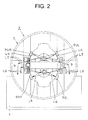
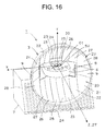
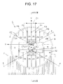
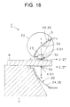
- FIGS. 16 , 17 , and 18 in order to clarify a structure of the invention, an upside movable reflector 13U, a downside movable reflector 13D, and a drive unit 14 are not shown. Further, in FIGS. 1 to 3 , and 8 to 11 a fin shape of a heat sink 7 is not shown.
- FIGS 1 to 28 are showing the embodiment 1 of vehicle lighting device on the present the invention.
- reference numeral 1 denotes a vehicle lighting device (vehicle headlamp) in the embodiment.
- the vehicle lighting device 1 illuminates light toward a forward direction of a vehicle by changing: a light distribution pattern for low beam passing (light distribution pattern for passing: first light distribution pattern), shown in FIG. 27 ; a light distribution pattern for high beam (light distribution pattern for cruising: second light distribution pattern), shown in FIG. 28 .
- the light distribution pattern LP for low beam having, shown in FIG 27 , an oblique cutoff line CL1 on a cruising lane side (left side) and a horizontal cutoff line CL2 on an opposite lane side (right side) with an elbow point E being a boundary.
- An angle formed between the oblique cutoff line CL1 and a horizontal line HL-HR of a screen is about 15 degrees.
- the light distribution pattern for high beam includes, shown in FIG. 28 , a first light distribution pattern HP1 for high beam, a second light distribution pattern HP2 for high beam, a third light distribution pattern HP3 for high beam, and a light distribution pattern LP1 for dimming low beam.
- the vehicle lighting device 1 is made up of: a fixed reflector 3 having an upside reflecting surface 2U (a first reflection surface, a first fixed reflection surface) and a downside reflecting surface 2D (a second reflection surface, a second fixed reflection surface) made of a parabola-based free curved face (NURBS-curved face); upside and downside movable reflectors 13U and 13D having upside and downside reflecting surfaces 12U (a first reflection surface, a first movable reflection surface, a movable reflection surface for second light distribution pattern) and 12D (a second reflection surface, a second movable reflection surface, a movable reflection surface for second light distribution pattern) made of a parabola-based free curved face (NURBS-curved face), similarly; an upside semiconductor-type light source 5U (a first semiconductor-type light source) and a downside semiconductor-type light source 5D (a second semiconductor-type light source) having a light emitting chip of a planar rectangle shape (planar elongated shape); a holder 6; a heat sink member
- the holder 6 is shaped like a plate having a top fixing face and a bottom fixing face.
- the holder 6 is made up of a resin member or a metal member with high thermal conductivity, for example.
- the heat sink member 7 is formed in a trapezoidal shape having an upper fixing face at its upper part, and is shaped like a fin from an intermediate part to a lower part.
- the heat sink member 7 is made up of a resin member or a metal member with high thermal conductivity, for example.
- the fixed reflector 3, the upside movable reflector 13U, the downside movable reflector 13D, the upside semiconductor-type light source 5U, the downside semiconductor-type light source 5D, the holder 6, the heat sink member 7, and the drive unit 14 constitute a lamp unit.
- the fixed reflector 3 is fixed and held on the holder 6.
- the upside movable reflector 13U and the downside movable reflector 13D are rotatably mounted on the holder 6 around a horizontal axis X.
- the upside semiconductor-type light source 5U is fixed and held on the top fixing face of the holder 6.
- the downside semiconductor-type light source 5D is fixed and held on the bottom fixing face of the holder 6.
- the holder 6 is fixed and held on the top fixing face of the hear sink member 7.
- the drive 6 is fixed and held on a top fixing face of the heat sink member 7.
- the drive unit 14 is fixed and held on the top fixing face of the holder 6 and the heat sink member 7
- the lamp units 3, 5U, 5D, 6, 7, 13U, 13D, 14 are disposed via an optical-axis adjustment mechanism, for example, in a lamp room partitioned by the lamp housing and the lamp lens. In the lamp room, apart from the lamp units 3, 5U, 5D, 6, 7, 13U, 13D, 14, other lamp units such as a fog lamp, a cornering lamp, a clearance lamp, and a turn signal lamp may be disposed.
- the upside reflecting surface 2U of the fixed reflector 3; the upside reflecting surface 12U of the upside movable reflector 13U; and the upside semiconductor-type light source 5U constitutes an upside unit (a first light source and reflecting surface unit) in which a light emitting face of the light emitting chip 4 is oriented upward in a vertical-axis Y direction.
- the downside reflecting surface 2D of the fixed reflector 3; the downside reflecting surface 12D of the downside movable reflector 13D; and the downside semiconductor-type light source 5D constitutes a downside unit (a second light source and reflecting surface unit) in which a light emitting face of the light emitting chip 4 is oriented downward in a vertical-axis Y direction.
- the upside units 2U, 5U, 12U, 13U and the downside units 2D, 5D, 12D, 13D, as shown in FIG. 17 are disposed in a point-symmetrical state with a point O being a center.
- a reflecting surface design of the upside reflecting surfaces 2U, 12U and a reflecting surface design of the downside reflecting surfaces 2D, 12D are not merely point-symmetrical (inverted).
- the fixed reflector 3 is made up of an optically opaque resin member or the like, for example.
- the fixed reflector 3 is substantially shaped like a rotational parabola-based face while an axis passing through the point-symmetrical point O is defined as a rotary axis.
- a front side of the fixed reflector 3 is opened in a substantial circle.
- a rear side of the fixed reflector 3 is closed.
- An elongated, substantially rectangular window portion 8 is provided at an intermediate part of the closed portion of the fixed reflector 3.
- the holder 6 is inserted into the window portion 8 of the fixed reflector 3.
- the fixed reflector 3 is fixed and held on the holder 6 at the outside (rear side) of the closed portion.
- the upside reflecting surface 2U and the downside reflecting surface 2D are provided, respectively at the upside and downside of the window portion 8.
- the upside reflecting surface 2U and the downside reflecting surface 2D made of a parabola-based free curved face (NURBS-curved face) has a reference focal point (pseudo-focal point) F and a reference optical axis (pseudo-optical axis) Z.
- An intermediate invalid reflection surface 9 is continually provided between the upside reflecting surface 2U and the downside reflecting surface 2D and at both the left and right sides of the window portion 8 of the inside (front side) of the closed portion of the fixed reflector 3.
- the intermediate invalid reflection surface 9 is a surface to which light beams (direct light beams) from the upside semiconductor-type light source 5U and the downside semiconductor-type light source 5D are disallowed to be incident.
- the upside reflecting surface 2U and the downside reflecting surface 2D of the fixed reflector 3 are made up of: a reflecting surface for low beam (a fixed reflection surface for first light distribution pattern and a fixed reflection surface for second light distribution pattern), forming the light distribution pattern LP for low beam and the light distribution pattern LP1 for dimming low beam; and a first reflecting surface for high beam (a fixed reflection surface for second light distribution pattern) and a second reflecting surface for high beam (a fixed reflection surface for second light distribution pattern), forming the first light distribution pattern HP 1 for high beam and the second light distribution pattern HP2 for high beam.
- the drive unit 14 is made up of a motor 15, a drive force transmission mechanism 16, and a spring for returning a mobile reflector (not shown).
- the motor 15 is directly fixed and held on the top fixing face of the heat sink member 7. In this manner, a heat generated at the time of supplying power to the motor 15 can be radiated (dissipated) to the outside at the heat sink member 7.
- the drive force transmission mechanism 16 is provided between the motor 15 and a respective one of the upside movable reflector 13U and the downside movable reflector 13D
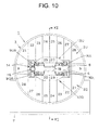
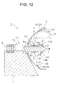
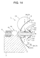
- the drive unit 14 rotates the upside movable reflector 13U and the downside movable reflector 13D with respect to the holder 6 around the horizontal-axis X between a first location (the location in a state shown in FIGS. 8 , 10 , 12 , and 14 ) and a second location (the location in a state shown in FIGS. 1 to 3 , 9, 11, 13, and 15 ).
- the upside movable reflector 13U and the downside movable reflector 13D are made up of an optically opaque resin member, for example.
- the upside movable reflector 13U and the downside movable reflector 13D, positioned in the second location, are substantially shaped like a rotational parabola-based face while an axis passing through the point-symmetrical point O is defined as a rotary axis.
- the front sides of the upside movable reflector 13U and the downside movable reflector 13D, positioned in the second location are opened in a substantial circle.
- the size of the opening i.e., an opening area at the front side of the upside movable reflector 13U and the downside movable reflector 13D is smaller than that of the opening, i.e., an opening area at the front side of the fixed reflector 3.
- Semicircular through holes 17 are provided at central parts of the upside movable reflector 13U and the downside movable reflector 13D, respectively.
- rectangular visor portions 18 are integrally provided at intermediate parts of the peripheral parts of the upside movable reflector 13U and the downside movable reflector 13D, respectively.
- the upside reflecting surface 12U and the downside reflecting surface 12D are provided on faces opposite to the upside semiconductor-type light source 5U of the upside movable reflector 13U and the downside semiconductor-type light source 5D of the downside movable reflector 13D, respectively.
- the upside reflecting surface 12U and the downside reflecting surface 12D that are made of a parabola-based free curved face has a reference focal point (pseudo-focal point) F1 and a reference optical axis (pseudo-optical axis) Z7.
- the upside reflecting surface 12U of the upside movable reflector 13U and the downside reflecting surface 12D of the downside movable reflector 13D are made of a third reflecting surface for high beam, forming the third light distribution pattern HP3 for high beam.
- the semiconductor-type light sources 5U, 5D are made up of: a board 10: the light emitting chip 4 provided on the board 10; and a sealing resin member 11 shaped like a thin rectangular solid, for sealing the light emitting chip 4.
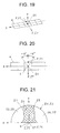
- the light emitting chip 4, as shown in FIGS. 19 and 20 arrays five square chips in a horizontal-axis X direction. One rectangular chip may be used.
- a center O1 of the light emitting chip 4 is positioned at or near reference focal points F, F1 of the reflecting surfaces 2U, 2D, 12U, 12D, and is positioned on reference optical axes Z, Z7 of the reflecting surfaces 2U, 2D, 12U, 12D.
- a light emitting face of the light emitting chip 4 (face opposite to opposite to a face opposed to the substrate 10) is oriented to the vertical-axis Y direction.
- the light emitting face of the light emitting chip 4 of the upside semiconductor-type light source 5U is oriented upward in the vertical-axis Y direction.
- the light emitting face of the light emitting chip 4 of the downside semiconductor-type light source 5D is oriented downward in the vertical-axis Y direction. Further, a long side of the light emitting chip 4 is parallel to a horizontal-axis X which is orthogonal to the reference optical axes Z, Z7 and the vertical axis Y.
- the horizontal axis X passes through the center O1 of the light emitting chip 4 or its vicinity (between the center O1 of the light emitting chip 4 and a long side at the rear side of the light emitting chip 4, and in this example, on the long side at the rear side of the light emitting chip 4), or alternatively, passes through the reference focal points F, F1 or its vicinity of the reflecting surfaces 2U, 2D, 12U, 12D.
- the horizontal axis X, the vertical axis Y, and the reference optical axes Z, Z7 constitute an orthogonal coordinate (X-Y Z orthogonal coordinate system) with the center O1 of the light emitting chip 4 serving as an origin.
- the horizontal axis X in the case of the upside unit 2U, 5U, 12U, the right side corresponds to a positive direction, and the left side corresponds to a negative direction; in the case of the downside units 2D, 5D, 12D, the left side corresponds to a positive direction and the right side corresponds to a negative direction.
- the upside corresponds to a positive direction; and the downside corresponds to a negative direction; and in the case of the downside units 2D, 5D, 12D, the downside corresponds to a positive direction, and the upside corresponds to a negative direction.
- the reference optical axes Z, Z7 in a respective one of the upside units 2U, 5U and the downside units 2D, 5D, the front side corresponds to a positive direction and the rear side corresponds to a negative direction.
- the reflecting surfaces 2U, 2D of the fixed reflector 3 and the reflecting surfaces 12U, 12D of the movable reflectors 13U, 13D are made up of a parabola-based free curved face (NURBS-curved face).
- the reference focal point F of the reflecting surfaces 2U, 2D of the fixed reflector 3 and the reference focal point F1 of the reflecting surfaces 12U, 12D of the movable reflector 13U, 13D are coincident or substantially coincident with each other; and are positioned on the reference optical axes Z, Z7 and between the center O1 of the light emitting chip 4 and a long side at the rear side of the light emitting chip 4. In this example, these points are positioned at the long side at the rear side of the light emitting chip 4.
- the reference focal-point distance of the reflecting surfaces 2U, 2D of the fixed reflector 3 is about 10 mm to 18 mm, and is greater than the reference focal-point distance F1 of the reflecting surfaces 12U, 12D of the movable reflectors 13U, 13D.
- the reference optical axis Z of the reflecting surfaces 2U, 2D of the fixed reflector 9 and the reference optical axis Z7 of the reflecting surfaces 12U, 12D of the movable reflectors 13U, 13D when they are positioned in the second location, are coincident or substantially coincident with each other.
- the optical axis Z are orthogonal to the horizontal axis X; and further, pass through the center O1 of the light emitting chip 4 or its vicinity.
- the reference optical axis Z7 of the reflecting surfaces 12U, 12D of the movable reflectors 13U, 13D is forward from the center O1 of the light emitting chip 4 or its vicinity and is upward with respect to the reference optical axis Z of the reflecting surfaces 2U, 2D of the fixed reflector 9.
- those illuminated toward the forward direction of the vehicle reflection light L4 reflected on the third reflecting surface for high beam are: reflection light L4 reflected on the third reflecting surface of a respective one of the movable reflectors 13U, 13D (the reflecting surfaces 12U, 12D) as the light distribution pattern HP3 for high beam; reflection light beams L5, L2 reflected on the first and second reflecting surfaces for high beam of the fixed reflector 3, shown in FIG. 28 as the first and second light distribution patterns HP1 and HP2 for high beam, shown in FIG.
- a light distribution pattern for high beam (light distribution pattern for cruising) is formed by the first light distribution pattern HP1 for high beam; the second light distribution pattern HP2 for high beam; the light distribution pattern HP3 for high beam; and the light distribution pattern LP1 for dimming low beam, and is illuminated toward the forward direction of the vehicle.
- the light distribution pattern LP for low beam shown in FIG. 27 .
- the movable reflectors 13U, 13D are positioned in the first location, the light from the light emitting chip 4, shaded by means of means of the movable reflectors 13U, 13D, is utilized as the first light distribution pattern HP1 for high beam and the second light distribution pattern HP2 for high beam.
- the reflecting surfaces 12U, 12D of the movable reflectors 13U, 13D are positioned in a range Z3 of high energy in an energy distribution Z2 of the light emitting chip 4.
- the light quantity of a respective one of the light distribution patterns HP1, HP2, HP3, LP1 for high beams (light distribution patterns for cruising), shown in FIG. 28 becomes greater than that of the light distribution pattern LP for low beam (light distribution pattern for passing), shown in FIG. 27 .
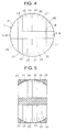
- the reflecting surfaces 2U, 2D are divided into eight sections in the vertical-axis Y direction and the central two are made up of segments 2I, 22, 23, 24, 25, 26, 27, 28, 29, 20, divided into two sections, respectively, in the horizontal-axis X direction.
- the second segment 22, the third segment 23, the fourth segment 24, the fifth segment 25, the sixth segment 26, and the seventh segment 27 at the central part and the peripheral part constitute the reflecting surface for low beam.
- the first segment 21 and the eighth segment 28 at both ends constitute the first reflecting surface for high beam.
- the ninth segment 29 and the tenth segment 20 at the central part constitute the second reflecting surface for high beam.
- the fourth segment 24 of the central part constitutes a first reflecting surface for low beam.
- the fifth segment 25 of the central part constitutes a second reflecting surface for low beam.
- the second segment 22, the third segment 23, the sixth segment 26, and the seventh segment 27 at an end part constitute a third reflecting surface for low beam.
- the fourth segment 24 of the first reflecting surface for low beam and the fifth segment 25 of the second reflecting surface for low beam, of the central part, are provided in the range Z1 between two longitudinal thick solid lines in FIG. 17 , with the range Z1 being a range in which the lattice dashed line in FIG. 21 is drawn, i.e., with the range Z1 being a range in which a longitude angle from the center O1 of the light emitting chip is ⁇ 40 degrees ( ⁇ O degrees in FIG. 20 ).
- the second segment 22, the third segment 23, the sixth segment 26, and the seventh segment 27 of the third reflecting surface for low beam of the end art are provided in a white-ground range in FIG. 21 other than the range Z1, i.e., in a range in which the longitude angle from the center O1 of the light emitting chip is ⁇ 40 degrees or more.
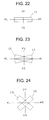
- a reflection image (screen map) of the light emitting chip 4 with a shape of a planar rectangle, obtained in a respective one of segments 22 to 27 of the reflecting surface for low beam among the reflecting surfaces 2U, 2D will be described referring to FIGS. 22, 23, and 24 .
- a reflection image 11 of the light emitting chip with a tilt angle of about 0 degrees is obtained with respect to a horizontal line HL-HR of a screen.
- a boundary P2 between the third segment 23 and the fourth segment 24 as shown in FIG.
- a reflection image 12 of the light emitting chip with a tilt angle of about 20 degrees is obtained with respect to the horizontal line HL-HR of the screen.
- a reflection image 13 of the light emitting chip 4 with a tilt angle of about 20 degrees is obtained with respect to the screen HL-HR of the screen.
- a reflection image 14 of the light emitting chip 4 with a tilt angle of about 40 degrees is obtained with respect to the horizontal line HL-HR of the screen.
- a reflection image 15 of the light emitting chip 4 with a tilt angle of about 40 degrees is obtained with respect to the horizontal line HL-HR of the screen.
- reflection images from the reflection image 11 with the tilt angle of about 0 degrees shown in FIG. 22 to the reflection image 12 with the tilt angle of about 20 degrees shown in FIG. 23 are obtained.
- reflection images from the reflection image 11 with the tilt angle of about 0 degrees shown in FIG. 22 to the reflection image 13 with the tilt angle of about 20 degrees shown in FIG. 23 are obtained.
- reflection images from the reflecting surface 12 with the tilt angle of about 20 degrees shown in FIG. 23 to the reflection image with the tilt angle of about 40 degrees shown in FIG. 24 are obtained.
- reflection images from the reflection images 13 with the tilt angle of about 20 degrees shown in FIG. 23 to the reflection image 15 with the tilt angle of about 40 degrees shown in FIG. 24 are obtained. Still furthermore, in the second segment 22 and the seventh segment 27 of the reflecting surface for low beam, a reflection image with a tilt angle of about 40 degrees or more is obtained.
- the reflection images from the reflection image 11 with the tilt angle of about 0 degree shown in FIG. 22 to the reflection images 12, 13 with the tilt angle of about 20 degrees shown in FIG. 23 are reflection images optimal to form a light distribution including an oblique cutoff line CL1 of the light distribution pattern LP for low beam.
- this is because it is easy to take the reflection images from the reflection image 11 with the tilt angle of about 0 degrees to the reflection images 12, 13 with the tilt angle of about 20 degrees along the oblique cutoff line CL1 1 with the tilt angle of about 15 degrees.
- reflection images which is not suitable to form a light distribution including the oblique cutoff line CL1 of the light distribution pattern LP for low beam.
- this is because, if the reflection image with the tilt angle of about 20 degrees or more is taken along the oblique cutoff line CL1 with the tilt angle of about 15 degrees, a light distribution becomes thick in a vertical direction, resulting in an excessive short-distance light distribution (i.e., light distribution with lowered long-distance visibility).
- a reflecting surface optimal to form the light distribution in the oblique cutoff line CL1 is determined depending upon a relative relationship between a range in which the reflection images 11, 12 within the tilt angle of 20 degrees, of a parabola-based, free curved reflecting surfaces, are obtained, and the energy distribution (Lambertian) of the semiconductor-type light sources 5U, 5D.
- the reflecting surface optimal to form the light distribution in the oblique cutoff line CL1 i.e., the fourth segment 24 and the fifth segment 25 are provided in the range Z1 1 in which the longitudinal angle is ⁇ 40 degrees from the center O1 1 of the light emitting chip 4, in which the reflection images 11, 12 within an angle (about 20 degrees) determined by adding about 5 degrees to the tilt angle (about 15 degrees) of the oblique cutoff line CL1 are obtained, and in the high-energy range Z3 in the energy distribution (Lambertian) Z2 of the light emitting chip 4.
- the first reflecting surface for low beam made of the fourth segment 24, as shown FIGS. 25 and 27 is a reflecting surface made of a free curved face for light-distributing and controlling the reflection images 11, 13 of the light emitting chip 4 in the range Z4 in the light distribution pattern LP for low beam, so that: the reflection images 11, 12 of the light emitting chip 4 do not run out of the oblique cutoff line CL1 and the horizontal cutoff line CL2; and a part of the reflection images 11, 12 of the light emitting chip 4 is substantially in contact with the oblique cutoff line CL1 and the horizontal cutoff line CL2.
- the second reflecting surface for low beam made of the fifth segment 5, as shown in FIGS. 26 and 27 is a reflecting surface made of light-distributing and controlling the reflection images 11, 13 of the light emitting chip 4 in the range Z5 containing the zone Z4 in the light distribution pattern LP for low beam, so that: the reflection images 11, 13 of the light emitting chip 4 do not run out of the oblique cutoff line CL1 and the horizontal cutoff line CL2 and a part of the reflection images 11, 13 of the light emitting chip 4 is substantially in contact with the oblique cutoff line CL1 and the horizontal cutoff line CL2; and so that: the density of a group of the reflection images 11, 13 of the light emitting chip 4 becomes lower than that of a group of the reflection images 11, 12 of the light emitting chip 4 according to the first reflecting surface for low beam made of the fourth segment 24; and the group of the reflecting surfaces 11, 13 of the light emitting chip 4 contains that of the reflection images 11, 12 of the light emitting chip 4 by the first reflecting surface for low beam made of the fourth
- the third reflecting surface for low beam made of the second segment 22, the third segment 23, the sixth segment 26, and the seventh segment 27, as shown in FIG. 27 is a reflecting surface made of a free curved face of light-distributing and controlling reflection images 14, 15 of the light emitting chip 4 in a range Z6 containing ranges Z4, Z5 in the light distribution pattern LP for low beam, so that: the reflection images 14, 15 of the light distribution chip 4 are substantially included in the light distribution pattern LP for low beam; the density of a group of the reflection images 14, 15 of the light emitting chip 4 becomes lower than that of a group of the reflection images 11, 12 of the light emitting chip 4 according to the first reflecting surface for low beam made of the fourth segment 24 and a group of the reflection images 11, 13 of the light emitting chip 4 according to the second reflecting surface for low beam made of the fifth segment 25; and the group of the reflection surfaces 14, 15 of the light emitting chip 4 contains that of the reflection images 11, 13 of the light emitting chip 4 according to the second reflecting surface for low beam made of the fifth segment 25.
- additional reflection surfaces 9UL, 9UR, 9DL, 9DR are provided for reflecting, on the intermediate invalid reflection surface 9, a part L6 of the light beams that are radiated from the light emitting chips 4 of the semiconductor-type light source 5U, 5D.
- the additional reflection surfaces 9UL, 9UR, 9DL, 9DR are positioned in a range other than a high energy range Z3 in energy distribution Z2 of the light emitting chips 4 of the semiconductor-type light sources 5U, 5D of the movable reflectors 13U, 13D when they are positioned in the second location.
- the additional reflection surfaces 9UL, 9UR, 9DL, 9DR as shown in FIG.
- a protrusive portion that is formed in the shape of a small square, which is provided at a site inclined at an angle of ⁇ 1 degree (about 60 degrees in this example) from a Y axis from among outer circumferential edge parts of the movable reflectors 13U, 13D when they are positioned in the second location that is viewed from a front side.
- the additional reflection surfaces 9UL, 9UR, 9DL, 9DR are the ones for reflecting, on the intermediate invalid reflection surface 9, a part L6 of the light beams that are radiated from the light emitting chips 4 of the semiconductor-type light sources 5U, 5D, by means of cross reflection.
- the additional reflection surfaces 9UL, 9DL at the left side as shown in FIG. 1 and FIG.
- FIG. 1 and FIG. 2 are the ones for reflecting, on the intermediate invalid reflection surfaces 9, 9R at the right side, a part L6 of the light beams that are radiated from the light emitting chips 4 of the semiconductor-type light sources 5U, 5D, by means of cross reflection
- the additional reflection surfaces 9UR, 9DR at the right side are the ones for reflecting, on the intermediate invalid reflection surfaces 9, 9L at the left side, a part L6 of the light beams that are radiated from the light emitting chips 4 of the semiconductor-type light sources 5U, 5D, by means of cross reflection.
- the vehicle lighting device 1 of the embodiment is made of the constituent elements as described above, and hereinafter, functions of the constituent elements will be described.
- an upside movable reflector 13U and a downside movable reflector 13D are positioned in a first position (the location in a state shown in FIGS. 8 , 10 , 12 , and 14 ).
- the upside movable reflector 13U and the downside movable reflector 13D are positioned in the first location due to a spring action and a stopper action which is not shown.
- a light emitting chip 4 of a respective one of the upside semiconductor-type light source 5U and the downside semiconductor-type light source 5D is lit to emit light.
- light is radiated from the light emitting chip 4 of the upside semiconductor-type light source 5U and the downside semiconductor-type light source 5D.
- a part of the light, i.e., reflection light L2 reflected on the second reflecting surface for high beam (the ninth segment 29 and the tenth segment 20) of the fixed reflector 3, as shown in FIG. 12 is shaded by means of means of the upside movable reflector 13U and the downside movable reflector 13D.
- the reflection light L3 is illuminated toward a forward direction of a vehicle, as a light distribution pattern LP for low beam, shown in FIG. 27 .
- Direct light (not shown) from the light emitting chip 4 of the upside semiconductor-type light source 5U and the downside semiconductor-type light source 5D is shaded by means of means of the upside movable reflector 13U and the downside reflector 13D, in particular by means of a visor portion 18.
- the optical paths in the downside reflecting surface 2D of the fixed reflector 3 and the downside reflecting surface 12D of the downside movable reflector 13D are not shown.
- reflection light from the first reflecting surface for low beam made of the fourth segment 24 of the reflecting surfaces 2U, 2D is light-distributed and controlled in the range Z4 in the light distribution pattern LP for low beam so that: the reflection images 11, 12 of the light emitting chip 4 does not run out of the oblique cutoff line CL1 and the horizontal cutoff line CL2; and a part of a respective one of the reflection images 11, 12 of the light emitting chip 4 is substantially in contact with the oblique cutoff line CL 1 and the horizontal cutoff line CL2.
- reflection light from the second reflecting surface for low beam made of the fifth segment 25 of the reflecting surfaces 2U, 2D is light-distributed and controlled in a range Z5 containing a range Z4 in the light distribution pattern LP for low beam, so that: the reflection images 11, 13 of the light emitting chip 4 do not run out of the oblique cutoff line CL1 1 and the horizontal cutoff line CL2 and a part of a respective one of the reflection images 11, 13 of the light emitting chip 4 is substantially in contact with the oblique cutoff line CL1 and the horizontal cutoff line CL2; and so that density of the group of the reflection images 11, 13 of the light emitting chip 4 becomes lower than that of the group of the reflection images 11, 12 of the light emitting chip 4 according to the first reflecting surface for low beam made of the fourth segment 24 and the group of the reflection images 11, 12 of the light emitting chip 4 contains that of the reflection images 11, 12 of the light emitting chip 4 according to the first reflecting surface for low beam made of the fourth segment 24.
- the reflection light from the third reflecting surface for low beam made of the second segment 22, the third segment 23, the sixth segment 26, and the seventh segment 27 of the reflecting surfaces 2U, 2D is light-distributed and controlled in the range Z6 containing the ranges Z4, Z5 in the light distribution pattern LP for low beam, so that: the reflection images 14, 15 of the light emitting chip 4 are substantially included in the light distribution pattern LP for low beam; the density of the group of the reflection images 14, 15 of the light emitting chip 4 becomes lower than that of the group of the reflection images 11, 12 of the light emitting chip 4 according to the first reflecting surface for low beam made of the fourth segment 24 and that of the group of the reflection images 11, 13 of the light emitting chip 4 according to the second reflecting surface for low beam made of the fifth segment 25; and the group of the reflection images 14, 15 of the light emitting chip 4 contains that of the reflection images 11, 12 of the light emitting chip 4 according to the first reflecting surface for low beam made of the fourth segment 24 and that of the reflection image 11, 13 of the light emitting chip 4 according to the
- a light distribution pattern LP for low beam is emitted forward of a vehicle.
- this vehicle lighting device 1 in the first embodiment is seen from a substantial front side, as shown in FIG. 5 .
- reflection surfaces for low beam a second segment 22, a third segment 23, a fourth segment 24, a fifth segment 25, a sixth segment 26, a seventh segment 27
- the upside reflection surface 2U and the downside reflection surface 2D of the fixed reflector 3 can be seen to be luminous.
- four corner parts outside of the portions seen to be luminous the outline portions in FIG. 5
- a part of the window portion 8 are seen as dark parts (the parts to which the grating pattern in FIG. 5 is applied).
- an area of these portions seen to be luminous is about 60% or more relative to that of the square surrounding the portion seen to be luminous, which is larger than that of the dark parts. Therefore, according to the vehicle lighting device 1 in the first embodiment, when the light distribution pattern LP for low beam, shown in FIG. 27 , is emitted forward of the vehicle, the entire lighting device is seen luminous; and therefore, even if the portions seen to be luminous are divided into top and bottom by means of the dark parts of the window portion 8, there is no problem in quality, visual recognition property, and appearance of the lighting device.
- the upside movable reflector 13U and the downside movable reflector 13D are positioned in a second location (the location in a state shown in FIGS. 1 to 3 , 9, 11, 13, and 15 ).
- a motor 15 is driven by supplying power to a motor 15 of a drive unit 14, a drive force of the motor 15 is transmitted to the upside movable reflector 13U and the downside movable reflector 13D via a drive force transmission mechanism 16; the upside movable reflector 13U and the downside movable reflector 13D rotate in synchronism from the first location to the second location against a spring force, and are positioned in the second location by means of a stopper action, although not shown.
- light is radiated from the light emitting chip 4 of the upside semiconductor-type light source 5U and the downside semiconductor-type light source 5D.
- the light radiated onto the reflecting surface for low beam (the second segment 22, the third segment 23, the fourth segment 24, the fifth segment 25, the sixth segment 26, the seventh segment 27) of the upside reflecting surface 2U and the downside reflecting surface 2D of the fixed reflector 3, and the remaining light having not been incident to the third reflecting surface (reflecting surfaces 12U, 12D) of the movable reflectors 13U, 13D, as shown in FIG. 13 , are reflected on the reflecting surface for low beam (the second segment 22, the third segment 23, the fourth segment 24, the fifth segment 25, the sixth segment 26, the seventh segment 27) of the fixed reflector 3; and the reflection light L3 is illuminated toward the forward direction of the vehicle, as the light distribution pattern LP1 for dimming low beam, shown in FIG. 28 .
- the upside movable reflector 13U and downside movable reflector 13D are positioned in the first location, light L1 radiated onto the first reflecting surface for high beam (the first segment 21 and the eighth segment 28) of the fixed reflector 3, shaded by means of the upside movable reflector 13U and the downside movable reflector 13D, as shown in FIG. 13 , is reflected on the first reflecting surface for high beam (the first segment 21 and the eighth segment 28) of the fixed reflector 3, and the reflection light L5 is illuminated toward the forward direction of the vehicle, as the light distribution pattern HP1 for high beam, shown in FIG. 28 .
- the optical paths in the downside reflecting surface 2D of the fixed reflector 3 and the downside reflecting surface 12D of the downside movable reflector 13D are not shown.
- a part L6 of the light beams that are radiated from the light emitting chips 4 of the upside semiconductor-type light source 5U and the downside semiconductor-type light source 5D is incident to the additional reflection surfaces 9UL, 9UR, 9DL, 9DR and then the incident light is cross-reflected on the intermediate invalid reflection surfaces 9, 9L, 9R by means of the additional reflection surfaces 9UL, 9UR, 9DL, 9DR.
- reflection light L7 cross-reflected on the additional reflection surfaces 9UL, 9DL at the left side, as shown in FIG 1 and FIG. 2 is incident to the intermediate invalid reflection surfaces 9, 9R at the right side
- the reflection light L7 cross-reflected on the additional reflection surfaces 9UR, 9DR at the right side is incident to the intermediate invalid reflection surfaces 9, 9L at the left side.
- the light L7 incident to the intermediate invalid reflection surfaces 9, 9L, 9R is emitted as reflection light L8 forward of the vehicle.
- the intermediate invalid reflection surfaces 9, 9L, 9R are also seen to be luminous by means of the reflection light L8.
- the first segment 21, the second segment 22, the third segment 23, the fourth segment 24, the fifth segment 25, the sixth segment 26, the seventh segment 27, the eighth segment 28, and the intermediate invalid reflection surfaces 9, 9L, 9R four corner parts outside of these portions seen to be luminous (the outline portions in FIG. 7 ) and a part of the window portion 8 are seen as dark parts (the parts to which the grating pattern in FIG. 7 is applied).
- an area of the portions seen to be luminous is about 60% or more relative to that of a square surrounding the portions seen to be luminous, and is larger than that of the dark parts.
- the portions seen to be luminous are vertically continuous at both of the left and right sides excluding the dark parts of the window portion 8 of a central portion, by means of the portions seen to be luminous, of the intermediate invalid reflection surfaces 9, 9L, 9R that are positioned at the left and right of the dark part of the window portion 8.
- the portions seen to be luminous correspond to the portions of the first segment 21, the second segment 22, the third segment 23, the fourth segment 24, the fifth segment 25, the sixth segment 26, the seventh segment 27, and the eighth segment 28.
- the four corner parts outside of the portions seen to be luminous the outline portions in FIG. 6
- a part of the window portion 8 and portions of the intermediate invalid reflection surfaces 9, 9L, 9R are seen to be dark parts (the parts to which the grating pattern in FIG. 6 is applied).
- an area of the portions seen to be luminous is about 60% or less relative to that of a square surrounding the portions seen to be luminous, and is not so different from that of the dark parts.
- the portions seen to be luminous are divided into a top and a bottom at a dark part of the window portion 8 at a central part and dark parts of the intermediate invalid reflection surfaces 9, 9L, 9R by means of the dark part of the window portion 8 and dark parts of the intermediate invalid reflection surfaces 9, 9L, 9R that are positioned at the left and right of the dark part of the window portion 8. Therefore, in the case of this vehicle lighting device, there is a problem in quality, visual recognition property, and appearance of the lighting device due to the aforementioned dark parts.
- a part L6 of the light beams that are radiated from the light emitting chips 4 of the upside semiconductor-type light source 5U and the downside semiconductor-type light source 5D is cross-reflected on the intermediate invalid reflection surfaces 9, 9L, 9R by means of the additional reflection surfaces 9UL, 9UR, 9DL, 9DR, so that the intermediate invalid reflection surfaces 9, 9L, 9R are seen to be luminous.
- the vehicle lighting device 1 in the first embodiment as described previously, when the light distribution patterns HP1, HP2, HP3, LP1 for high beam, shown in FIG. 28 , are emitted forward of the vehicle, the entire lighting device is seen to be substantially luminous; and therefore, there is no problem in quality, visual recognition property, and appearance of the lighting device.
- the vehicle lighting device 1 of the embodiment is made of the constituent elements and functions, as described above, and hereinafter, advantageous effect(s) thereof will be described.
- the vehicle lighting device 1 in the first embodiment when the movable reflectors 13U, 13D are positioned in the second location, a part L6 of the light beams that are radiated from the semiconductor-type light sources 5U, 5D is reflected on the additional reflection surfaces 9UL, 9UR, 9DL, 9DR and then the reflected light L7 is incident to the intermediate invalid reflection surfaces 9, 9L, 9R, so that there is allowed to be luminous the intermediate invalid reflection surfaces 9, 9L, 9R between: the fixed reflection surface for second light distribution pattern, which are more outside than the fixed reflection surface for first light distribution pattern of the first fixed reflection surface (the first segment 21 and the eighth segment 28 that are more outside than the second segment 22, the third segment 23, the fourth segment 24, the fifth segment 25, the sixth segment 26, and the seventh segment 27 of the upside reflection surface 2U); and the fixed reflection surface for second light distribution pattern, which is more outside than the fixed reflection surface for first light distribution pattern of the second fixed reflection surface (the first segment 21 1 and the eighth segment 28 that are more outside than the second segment 22, the third
- the vehicle lighting device 1 in the first embodiment is capable of eliminating a dark part between: the fixed reflection surfaces for second light distribution pattern, which are more outside than the fixed reflection surfaces for first light distribution pattern of the first fixed reflection surface (i.e., the first segment 21 and the eighth segment 28 of the upside reflection surface 2U); and the fixed reflection surfaces for second light distribution pattern, which are more outside than the fixed reflection surfaces for first light distribution pattern of the second fixed reflection surface (i.e., the first segment 21 and the eighth segment 28 of the downside reflection surface 2D).
- the vehicle lighting device 1 in the first embodiment is capable of substantially entirely illuminating: the fixed reflection surfaces for second light distribution pattern of the first fixed reflection surface (the first segment 21 and the eighth segment 28 of the upside reflection surface 2U); fixed reflection surfaces for second light distribution pattern of the second fixed reflection surface (the first segment 21 and the eight segment 28 of the downside reflection surface 2D); and the intermediate invalid reflection surface 9, 9L, 9R between the fixed reflection surfaces for second light distribution pattern, which are more outside than the fixed reflection surfaces for first light distribution pattern of the first fixed reflection surface (the first segment 21 and the eighth segment 28 of the upper reflection surface 2U), and the fixed reflection surfaces for second light distribution pattern, which are more outside than the fixed reflection surfaces for first light distribution pattern of the second fixed reflection surface (the first segment 21 and the eighth segment 28 of the downside reflection surface 2D).
- the vehicle lighting device 1 in the first embodiment is improved in quality, is also improved in visual recognition property, and further, is improved in appearance, in comparison with the conventional vehicle lighting device in which a nonluminous dark part may be formed,.
- the additional reflection surfaces 9UL, 9UR, 9DL, 9DR are positioned in a range other than a high energy range Z3 in energy distribution of the semiconductor-type light sources 5U, 5D of the movable reflectors 13U, 13D when they are positioned in the second location.
- the vehicle lighting device 1 in the first embodiment when the movable reflectors 13U, 13D are positioned in the second location, the light with high energy in energy distribution of the semiconductor-type light source 5U, 5D is disallowed to be interfered with the additional reflection surfaces 9UL, 9UR, 9DL, 9DR (protrusive portions formed in the shape of small squares in which the additional reflection surfaces 9UL, 9UR, 9DL, 9DR are provided at interior faces by means of reflection surface processing) from being reliably incident to a respective one of the fixed reflection surfaces for second light distribution pattern of the first fixed reflection surface and the second fixed reflection surfaces (the first segment 21 and the eighth segment 28 of the upside reflection surface 2U and the downside reflection surface 2D) and the movable reflection surfaces for second light distribution pattern of the first movable reflection surface and the second movable reflection surface (the upside reflection surface 12U and the downside reflection surface 12D).
- the additional reflection surfaces 9UL, 9UR, 9DL, 9DR protrusive portions formed in the shape of small squares in which the additional reflection surfaces 9
- the light with high energy in energy distribution of the semiconductor-type light sources 5U, 5D is reliably incident to a respective one of the fixed reflection surface for second light distribution pattern of the first fixed reflection surface and the second fixed reflection surface (the first segment 21 and the eighth segment 28 of the upside reflection surface 2U and the downside reflection surface 2D) and the movable reflection surface for second light distribution pattern of the first movable reflection surface and the second movable reflection surface (the upside reflection surface 12U and the downside reflection surface 12D).
- the light quantity (lightness, luminance, luminous flux) of the predetermined second light distribution patterns is disallowed be decreased by means of the additional reflection surfaces 9UL, 9UR, 9DL, 9DR (the protrusive portions formed in the shape of small squares in which the additional reflection surfaces 9UL, 9UR, 9DL, 9DR are provided at interior faces by means of reflection surface processing).
- the additional reflection surfaces 9UL, 9UR, 9DL, 9DR are positioned in a range other than a high energy range Z3 in energy distribution of the semiconductor-type light sources 5U, 5D of the movable reflectors 13U, 13D when they are positioned in the second location.
- the vehicle lighting device 1 in the first embodiment when the movable reflectors 13U, 13D are positioned in the first location, the light beams from the semiconductor-type light sources 5U, 5D are disallowed to be interfered with the additional reflection surfaces 9UL, 9UR, 9DL, 9DR (the protrusive portions formed in the shape of small squares in which the additional reflection surfaces 9UL, 9UR, 9DL, 9DR are provided on interior faces by means of reflection surface processing) from being incident to a respective one of the fixed reflection surfaces for first light distribution pattern of the first fixed reflection surface and the second fixed reflection surface (the first segment 21 and the eighth segment 28 that are more outside than the second segment 22, the third segment 23, the fourth segment 24, the fifth segment 25, the sixth segment 26, and the seventh segment 27 of the upside reflection surface 2U and the downside reflection surface 2D).
- the additional reflection surfaces 9UL, 9UR, 9DL, 9DR the protrusive portions formed in the shape of small squares in which the additional reflection surfaces 9UL, 9UR, 9DL, 9DR are provided on interior faces by means
- the light beams from the two semiconductor-type light sources 5U, 5D are reliably incident to a respective one of the fixed reflection surfaces for first light distribution pattern of the first fixed reflection surface and the second fixed reflection surface (the first segment 21 and the eighth segment 28 that are more outside than the second segment 22, the third segment 23, the fourth segment 24, the fifth segment 25, the sixth segment 26, and the seventh segment 27 of the upside reflection surface 2U and the downside reflection surface 2D).
- the light quantity (lightness, luminance, luminous flux) of a predetermined first light distribution pattern (the light distribution pattern LP for low beam, shown in FIG. 27 ) is disallowed to be decreased by means of the additional reflection surfaces.
- the fixed reflector 3 and the movable reflectors 13U, 13D are formed in the shape of a substantially rotating parabolic face, so that a part L6 of the light beams that are radiated from the semiconductor-type light sources 5U, 5D can be cross-reflected easily and reliably on the intermediate invalid reflections 9, 9L, 9R by means of the additional reflection surfaces 9UL, 9UR, 9DL, 9DR.
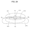
- FIG. 29 shows a second embodiment of a vehicle lighting device according to the present invention.
- the vehicle lighting device in the second embodiment will be described.
- like constituent elements shown in FIG. 1 to FIG. 28 are designated by like reference numerals.
- the vehicle lighting device 1 in the first embodiment when the movable reflectors 13U, 13D are positioned in the second location, the light distribution patterns HP1, HP2, HP3, LP1 for high beam are obtained.
- the vehicle lighting device in the second embodiment when the movable reflectors 13U, 13D are positioned in at least the second location, i.e., when the movable reflectors 13U, 13D are positioned in the second location, the light distribution patterns HP1, HP2, HP3, LP1 for high beam are obtained as described previously and when the movable reflectors 13U, 13D are positioned in a third location (the position proximal to the second location), light distribution patterns DP1, DP2, DP3, DP4, DP5 for daytime running light are obtained as shown in FIG. 29 .
- first and second embodiments describe a light distribution pattern LP for low beam.
- a light distribution pattern other than the light distribution pattern LP for low beam for example, a light distribution pattern having an oblique cutoff line on a driving lane side and a horizontal cutoff line on an opposite lane side with an elbow point being a turning point, such as a light distribution pattern for expressway or a light distribution pattern for fog lamp.
- first and second embodiments describe a vehicle lighting device 1 for left side driving lane.
- the present invention can be applied to a vehicle lighting device for right side driving lane.
- the light distribution pattern LP for low beam, shown in FIG. 27 , and the light distribution patterns HP1, HP2, HP3, LP1 for high beam, shown in FIG. 28 are switched to each other by using the movable reflectors 13U, 13D, or alternatively, there are switched to each other the light distribution pattern LP for low beam, shown in FIG. 27 ; the light distribution patterns HP1, HP2, HP3, LP1 for high beam, shown in FIG. 28 ; and the light distribution patterns DP1, DP2, DP3, DP4, DP5 for daytime running light, shown in FIG. 29 .
- the light distribution patterns DP1, DP2, DP3, DP4, DP5 for daytime running light, shown in FIG. 29 may be obtained by means of only the fixed reflector 3 without use of the movable reflectors 13U, 13D.
- an additional reflection surface is provided in a range other than a high energy range Z3 in energy distribution of the semiconductor-type light sources 5U, 5D of the fixed reflector 3, i.e., in a range of an X-axis side more than the double-dotted chain line, as shown in FIG. 17 .
- the foregoing first and second embodiments describe a headlamp (a vehicle headlamp) which is adapted to switch the light distribution pattern LP for low beam, shown in FIG. 27 , and the light distribution patterns HP1, HP2, HP3, LP1 for high beam, shown in FIG. 28 , to each other, or alternatively, to switch the light distribution pattern LP for low beam, shown in FIG. 27 ; the light distribution patterns HP1, HP2, HP3, LP1 for high beam, shown in FIG. 28 ; and the light distribution patterns DP1, DP2, DP3, DP4, DP5 for daytime running light, shown in FIG. 29 , to each other.
- the present invention can be applied to a lamp other than a fog lamp, a tail lamp, or a stop lamp other than the headlamp.
Landscapes
- Engineering & Computer Science (AREA)
- General Engineering & Computer Science (AREA)
- Physics & Mathematics (AREA)
- Microelectronics & Electronic Packaging (AREA)
- Optics & Photonics (AREA)
- Non-Portable Lighting Devices Or Systems Thereof (AREA)
- Lighting Device Outwards From Vehicle And Optical Signal (AREA)
Abstract
Description
- This application claims priority of Japanese Patent Application No.
2010-110109 filed on May 12, 2010 - The present invention relates to a vehicle lighting device which is comprised of two light source/reflection surface units.
- A vehicle lighting device of such type is conventionally known (for example, Japanese Patent Application Laid-open No.
2006-24509 - However, in the conventional vehicle lighting device, two light emitting units for lighting device, a respective one of which is comprised of an LED and a reflection surface, are disposed at the top and the bottom of the lighting device. Therefore, in the conventional vehicle lighting device, a nonluminous portion to which the light beams from the top and bottom LEDs are disallowed to be incident, i.e., a dark part may be formed between the top and bottom light emitting units for lighting device.
- The problem to be solved by the present invention is that, in the conventional vehicle lighting device, a nonluminous portion to which the light beams from the top and bottom LEDs are disallowed to be incident, i.e., a dark part may be formed between the top and bottom light emitting units for lighting device.
- A vehicle lighting device of
claim 1 in the present invention which is comprised of two light source/reflection surface units, said device comprising: - a first light source/reflection surface unit which is comprised of a first semiconductor-type light source and a first reflection surface for reflecting and emitting light from the first semiconductor-type light source as a predetermined light distribution pattern;
- a second light source/reflection surface unit which is comprised of a second semiconductor-type light source and a second reflection surface for reflecting and emitting light from the second semiconductor-type light source as a predetermine light distribution pattern;
- a holder which is disposed between the first light source/reflection surface unit and the second light source/reflection source unit and by which the first light source/reflection surface unit and the second light source/reflection surface unit are held;
- an intermediate invalid reflection surface which is continuously provided between the first reflection surface and the second reflection surface and to which the light from the first semiconductor-type light source and the light from the second semiconductor-type light source are disallowed to be incident; and
- an additional reflection surface for reflecting to the intermediate invalid reflection surface, the light from the first semiconductor-type light source and the light from the second semiconductor-type light source.
- The vehicle lighting device of claim 2 in the present invention, wherein:
- the first reflection surface is made of: a first fixed reflection surface which is provided at a fixed reflector; and a first movable reflection surface which is provided at a movable reflector;
- the second reflection surface is made of: a second fixed reflection surface which is provided at a fixed reflector; and a second movable reflection surface which is provided at a movable reflector;
- the first fixed reflection surface and the second fixed reflection surface are comprised of: a fixed reflection surface for first light distribution pattern, for reflecting and emitting a predetermined first light distribution pattern, when the movable reflector is positioned in a first location; and a fixed reflection surface for second light distribution pattern, for reflecting and emitting a predetermined second light distribution pattern, when the movable reflector is positioned in a second location;
- the first movable reflection surface and the second movable reflection surface are comprised of a movable reflection surface for second light distribution pattern, for reflecting and emitting a predetermined second light distribution pattern, when the movable reflector is positioned in a second location;
- the intermediate invalid reflection surface is continuously provided between the fixed reflection surface for the second light distribution pattern, which is more outside than the fixed reflection surface for first light distribution pattern of the first fixed reflection surface, and the fixed reflection surface for the second light distribution pattern, which is more outside than the fixed reflection surface for first light distribution pattern of the second fixed reflection surface; and
- the additional reflection surface is positioned in a range other than a high energy range in energy distribution of the first semiconductor-type light source and the second semiconductor-type light source of the movable reflector, when the movable reflector is positioned in the second location.
- The vehicle lighting device of
claim 3 in the present invention, wherein: - the first reflection surface is made of a first fixed reflection surface which is provided at a fixed reflector;
- the second reflection surface is made of a second fixed reflection surface which is provided at a fixed reflector;
- the first fixed reflection surface and the second fixed reflection surface are comprised of a reflection surface for reflecting and emitting a predetermined light distribution pattern;
- the intermediate invalid reflection surface is continuously provided between the first fixed reflection surface and the second fixed reflection surface; and
- the additional reflection surface is positioned in a range other than a high energy range in energy distribution of the first semiconductor-type light source and the second semiconductor-type light source, of the fixed reflector.
- The vehicle lighting device of
claim 4 in the present invention, wherein the fixed reflector and the movable reflector is formed in a shape of a rotating parabolic face. The vehicle lighting device of claim 5 in the present invention, wherein the fixed reflector is formed in a shape of a rotating parabolic face. - In the vehicle lighting device of the present invention (the invention according to claim 1), by means for solving the problem described previously, if a first semiconductor-type light source and a second semiconductor-type light source are illuminated to emit light, a major part of light that is radiated from the first semiconductor-type light source is reflected and emitted as a predetermined light distribution pattern on a first reflection surface; and a major part of light that is radiated from a second semiconductor-type light source is reflected and emitted as a predetermined light distribution pattern on a second reflection surface. Moreover, in the vehicle lighting device of the present invention (the invention according to claim 1), a remaining portion of a respective one of the light beams that are radiated from the first semiconductor-type light source and the second semiconductor-type light source is reflected on an additional reflection surface and then the reflected light is incident to an intermediate invalid reflection surface, so that the intermediate invalid reflection surface between the first reflection surface and the second reflection surface is allowed to be luminous. As a result, the vehicle lighting device of the present invention (the invention according to claim 1) is capable of eliminating a dark part between the first reflection surface and the second reflection surface. In other words, the vehicle lighting device of the present invention (the invention according to claim 1) is capable of substantially entirely illuminate the intermediate invalid reflection surface between the first reflection surface and the second reflection surface, the first reflection surface, and the second reflection surface. In this manner, the vehicle lighting device of the present invention (the invention according to claim 1) is improved in quality, is also improved in visual recognition property, and further, is improved in appearance, in comparison with the conventional vehicle lighting device in which a nonluminous dark part may be formed between top and bottom light emitting units for lighting device.
- In addition, in the vehicle lighting device of the present invention (the invention according to claim 2), by means for solving the problem described above, when a movable reflector is positioned in a first location, a predetermined first light distribution pattern is reflected and emitted from a fixed reflection surface for first light distribution pattern of a first fixed reflection surface and a second fixed reflection surface; and when the movable reflector is positioned in a second location, a predetermined second light distribution pattern is reflected and emitted from a respective one of a fixed reflection surface for second light distribution pattern of the first fixed reflection surface and the second fixed reflection surface and a movable reflection surface for second light distribution pattern of a first movable reflection surface and a second movable reflection surface. Moreover, in the vehicle lighting device of the present invention (the invention according to claim 2), when the movable reflector is positioned in a second location, a part of light beams that are radiated from a first semiconductor-type light source and a second semiconductor-type light source is reflected on an additional reflection surface and then the reflected light is incident to an intermediate invalid reflection surface, so that the intermediate invalid reflection surface can be illuminated between a fixed reflection surface for second light distribution pattern, which is more outside than the fixed reflection surface for first light distribution pattern of the first fixed reflection surface, and a fixed reflection surface for second light distribution pattern, which is more outside than the fixed reflection surface for first light distribution pattern of the second fixed reflection surface. As a result, the vehicle lighting device of the present invention (the invention according to claim 2) is capable of eliminating a dark part between the fixed reflection surface for second light distribution pattern, which is more outside than the fixed reflection surface for first light distribution pattern of the first fixed reflection surface, and the fixed reflection surface for second light distribution pattern, which is more outside than the fixed reflection surface for first light distribution pattern of the second fixed reflection surface. In other words, the vehicle lighting device of the present invention (the invention according to claim 2) is capable of substantially entirely illuminating: the fixed reflection surface for second light distribution pattern of the first fixed reflection surface; the fixed reflection surface for second light distribution pattern of the second fixed reflection surface; and the intermediate invalid reflection surface between the fixed reflection surface for second light distribution pattern, which is more outside than the fixed reflection surface for first light distribution pattern of the first fixed reflection surface, and the fixed reflection surface for second light distribution pattern, which is more outside than the fixed reflection surface for first light distribution pattern of the second fixed reflection surface. In this manner, the vehicle lighting device of the present invention (the invention according to claim 2) is improved ins quality, is also improved in visual recognition property, and further, is improved in appearance, in comparison with the conventional vehicle lighting device in which a nonluminous dark part may be formed between top and bottom light emitting units for lighting device.
- In particular, in the vehicle lighting device of the present invention (the invention according to claim 2), an additional reflection surface is positioned in a range other than a high energy range in energy distribution of a first semiconductor-type light source and a second semiconductor-type light source of a movable reflector when it is positioned in a second location. As a result, in the vehicle lighting device of the present invention (the invention according to claim 2), when the movable reflector is positioned in the second location, the light beams with high energy in energy distribution of the first semiconductor-type light source and the second semiconductor-type light source is disallowed to be interfered with the additional reflection surface from being incident to the fixed reflection surface for second light distribution pattern of the first fixed reflection surface and the second fixed reflection surface and the movable reflection surface for second light distribution pattern of the first movable reflection surface and the second movable reflection surface, respectively. In the vehicle lighting device of the present invention (the invention according to claim 2), when the movable reflector is positioned in the second location, the light beams with high energy in energy distribution of the first semiconductor-type light source and the second semiconductor-type light source are reliably incident to the fixed reflection surface for second light distribution pattern of the first fixed reflection surface and the second fixed reflection surface and the movable reflection surface for second light distribution pattern of the first movable reflection surface and the second movable reflection surface, respectively. Thus, the light quantity (lightness, luminance, luminous flux) of the predetermined second light distribution pattern is disallowed to be decreased by means of the additional reflection surface.
- Moreover, in the vehicle lighting device of the present invention (the invention according to claim 2), an additional reflection surface is positioned in a range other than a high energy range in energy distribution of a first semiconductor-type light source and a second semiconductor-type light source of a movable reflector when it is positioned in a second location. As a result, in the vehicle lighting device of the present invention (the invention according to claim 2), when the movable reflector is positioned in a first location, a respective one of light beams from the first semiconductor-type light source and the second reflector-type light source is disallowed to be interfered with the additional reflection surface from being incident to the fixed reflection surface for first light distribution pattern of the first fixed reflection surface and the second fixed reflection surface. In this manner, in the vehicle lighting device of the present invention (the invention according to claim 2), when the movable reflector is positioned in the first location, the respective one of the light beams from the first semiconductor-type light source and the second semiconductor-type light source is reliably incident to the fixed reflection surface for first light distribution pattern of the first fixed reflection surface and the second fixed reflection surface. Thus, the light quantity (lightness, luminance, luminous flux) of the predetermined first light distribution pattern is disallowed to be decreased on the additional reflection surface.
- Further, in the vehicle lighting device of the present invention (the invention according to claim 3), by means for solving the problem described previously, if a first semiconductor-type light source and a second semiconductor-type light source are illuminated to emit light, a major part of light beams that are radiated from the first semiconductor-type light source and the second semiconductor-type light source are reflected and emitted as a predetermined light distribution pattern on a first fixed reflection surface and a second fixed reflection surface. Moreover, in the vehicle lighting device of the present invention (the invention according to claim 3), a remaining part of a respective one of the light beams that are radiated from the first semiconductor-type light source and the second semiconductor-type light source is reflected on an additional reflection surface and then the reflected light is incident to an intermediate invalid reflection surface, so that the intermediate invalid reflection surface between the first fixed reflection surface and the second fixed reflection surface can be illuminated. As a result, the vehicle lighting device of the present invention (the invention according to claim 3) is capable of eliminating a dark part between the first fixed reflection surface and the second fixed reflection surface. In other words, in the vehicle lighting device of the present invention (the invention according to claim 3) is capable of substantially entirely illuminate the first fixed reflection surface, the second fixed reflection surface, and the intermediate invalid reflection surface between the first fixed reflection surface and the second fixed reflection surface. In this manner, the vehicle lighting device of the present invention (the invention according to claim 3) is improved in quality, is also improved in visual recognition property, and further, is improved in appearance, in comparison with the conventional vehicle lighting device in which a nonluminous dark part may be formed between top and bottom light emitting units for lighting device.
- In particular, in the vehicle lighting device of the present invention (the invention according to claim 3), an additional reflection surface is positioned in a range other than a high energy range in energy distribution of a first semiconductor-type light source and a second semiconductor-type light source of a fixed reflector. As a result, in the vehicle lighting device of the present invention (the invention according to claim 3), light beams with high energy in energy distribution of the first semiconductor-type light source and the second semiconductor-type light source is disallowed to be interfered with the additional reflection surface from being incident to the first fixed reflection surface and the second fixed reflection surface, respectively. In this manner, in the vehicle lighting device of the present invention (the invention according to claim 3), the light beams in energy distribution of the first semiconductor-type light source and the second semiconductor-type light source are reliably incident to the first fixed reflection surface and the second fixed reflection surface, respectively. Thus, the light quantity (lightness, luminance, luminous flux) of the predetermined light distribution pattern is disallowed to be decreased by means of the additional reflection surface.
- Furthermore, in the vehicle lighting device of the present invention (the invention according to
claims 4 or 5), the fixed reflector and the movable reflector according to claim 2 or the fixed reflector according toclaim 3 are formed in the shape of a rotating parabolic face. Therefore, in the vehicle lighting device of the present invention (the invention according to claim 4), a part of the light beams that are radiated from the first semiconductor-type light source and the second semiconductor-type light source can be cross-reflected easily and reliably on an intermediate invalid reflection surface by means of an additional reflection surface. -
-
FIG. 1 shows a first embodiment of a vehicle lighting device according to the present invention, and is an explanatory perspective view of an optical path in an additional reflection surface and an intermediate invalid reflection surface when an upside movable reflector and a downside movable reflector are positioned in a second location. -
FIG. 2 is an explanatory front view showing an optical path in the additional reflection surface and the intermediate invalid reflection surface when the upside movable reflector and the downside movable reflector are positioned in the second location, similarly. -
FIG. 3 is an explanatory front view showing a range in which the additional reflection surface is positioned when the upside movable reflector and the downside movable reflector are positioned in the second location, similarly. -
FIG. 4 is an explanatory front view showing an upside reflection surface, a downside reflector surface, and the intermediate invalid reflection surface, similarly. -
FIG. 5 is an explanatory front view showing a range in which the upside reflection surface and the downside reflection surface are illuminated when the upside movable reflector and the downside movable reflector are positioned in a first location and then a light distribution pattern for low beam is reflected and emitted, similarly. -
FIG. 6 is an explanatory front view showing a range in which, in a case where no additional reflection surface exists, the upside reflection surface and the downside reflection surface are illuminated when the upside movable reflector and the downside movable reflector are positioned in the second location and then a light distribution pattern for high beam is reflected and emitted, similarly. -
FIG. 7 is an explanatory front view showing a range in which the upside reflection surface, the downside reflection surface, and the intermediate invalid reflection surface are illuminated when the upside movable reflector and the downside movable reflector are positioned in the second location and then the light distribution pattern for high beam is reflected and emitted, similarly. -
FIG. 8 is a perspective view of essential parts when the upside movable reflector and the downside movable reflector are positioned in the first location, similarly. -
FIG. 9 is a perspective view of essential parts when the upside movable reflector and the downside movable reflector are positioned in the second location, similarly. -
FIG. 10 is a perspective view of essential parts when the upside movable reflector and the downside movable reflector are positioned in the first location, similarly. -
FIG. 11 is a perspective view of essential parts when the upside movable reflector and the downside movable reflector are positioned in the second location, similarly. -
FIG. 12 is a sectional view taken along the line VII-VII inFIG. 10 showing an optical path, similarly. -
FIG. 13 is a sectional view taken along the line VIII-VIII inFIG. 11 showing an optical path, similarly. -
FIG. 14 is a sectional view taken along the line XII-XII inFIG. 10 showing an energy distribution of a semiconductor-type light source, similarly. -
FIG. 15 is a sectional view taken along the line XIII-XIII inFIG. 11 showing an energy distribution of a semiconductor-type light source, similarly. -
FIG. 16 is a perspective view showing essential parts when the upside movable reflector, the downside movable reflector, and a drive unit are not shown, similarly. -
FIG. 17 is a front view showing essential parts when the upside movable reflector, the downside movable reflector, and the drive unit are not shown, similarly. -
FIG. 18 is a sectional view taken along the line XII-XII inFIG. 17 , similarly. -
FIG. 19 is an explanatory perspective view showing a relative position relationship between a center of a light emitting chip and a reference focal point of a reflection surface, similarly. -
FIG. 20 is an explanatory plan view showing the relative position relationship between the center of the light emitting chip and the reference focal point of the reflection surface, similarly. -
FIG. 21 is an explanatory plan view showing a range in which a first reflection surface made of a fourth segment and a second reflection surface made of a fifth segment are provided, similarly. -
FIG. 22 is an explanatory view showing a reflection image of a light emitting chip, obtained at a point P1 of a reflection surface, similarly. -
FIG. 23 is an explanatory view showing a reflection image of a light emitting chip, obtained at points P2, P3 of a reflection surface, similarly. -
FIG. 24 is an explanatory view showing a reflection image of a light emitting chip, obtained at points P4, P5 of a reflection surface, similarly. -
FIG. 25 is an explanatory view showing a reflection image group of a light emitting chip, obtained by means of the first reflection surface made of the fourth segment, similarly. -
FIG. 26 is an explanatory view showing a reflection image group of a light emitting chip, obtained by means of the second reflection surface made of the fifth segment, similarly. -
FIG. 27 is an explanatory view showing a light distribution pattern for low beam, having an oblique cutoff line and a horizontal cutoff line, similarly. -
FIG. 28 is an explanatory view showing a light distribution pattern for high beam, similarly. -
FIG. 29 shows a second embodiment of a vehicle lighting device according to the present invention, and is an explanatory view showing a light distribution pattern for daytime running light. - Hereinafter, embodiments of a vehicle headlamp according to the present invention will be described in detail, referring to the drawings. In the drawings, the letter sign "VU-VD" designates a vertical line of a top and a bottom of a screen; and the letter sign "HL-HR" designates a horizontal line of a left and a right of the screen.
FIGS. 25 and 26 are explanatory views showing a reflection image group of a light emitting chip on the screen obtained by computer simulation. In the specification and claims, the terms "top", "bottom", "front", "rear", "left", and "right" designate the top, bottom, front, rear, left, and right of a vehicle when the vehicle headlamp according to the present invention is mounted on a vehicle (automobile). In addition, inFIGS. 16 ,17 , and18 , in order to clarify a structure of the invention, an upsidemovable reflector 13U, a downsidemovable reflector 13D, and adrive unit 14 are not shown. Further, inFIGS. 1 to 3 , and8 to 11 a fin shape of aheat sink 7 is not shown. -
FIGS 1 to 28 are showing theembodiment 1 of vehicle lighting device on the present the invention. Hereinafter, a configuration of a vehicle lighting device in the embodiment will be described. In the figures,reference numeral 1 denotes a vehicle lighting device (vehicle headlamp) in the embodiment. Thevehicle lighting device 1 illuminates light toward a forward direction of a vehicle by changing: a light distribution pattern for low beam passing (light distribution pattern for passing: first light distribution pattern), shown inFIG. 27 ; a light distribution pattern for high beam (light distribution pattern for cruising: second light distribution pattern), shown inFIG. 28 . - The light distribution pattern LP for low beam having, shown in
FIG 27 , an oblique cutoff line CL1 on a cruising lane side (left side) and a horizontal cutoff line CL2 on an opposite lane side (right side) with an elbow point E being a boundary. An angle formed between the oblique cutoff line CL1 and a horizontal line HL-HR of a screen is about 15 degrees. The light distribution pattern for high beam includes, shown inFIG. 28 , a first light distribution pattern HP1 for high beam, a second light distribution pattern HP2 for high beam, a third light distribution pattern HP3 for high beam, and a light distribution pattern LP1 for dimming low beam. - The
vehicle lighting device 1 is made up of: a fixedreflector 3 having anupside reflecting surface 2U (a first reflection surface, a first fixed reflection surface) and adownside reflecting surface 2D (a second reflection surface, a second fixed reflection surface) made of a parabola-based free curved face (NURBS-curved face); upside and downsidemovable reflectors downside reflecting surfaces 12U (a first reflection surface, a first movable reflection surface, a movable reflection surface for second light distribution pattern) and 12D (a second reflection surface, a second movable reflection surface, a movable reflection surface for second light distribution pattern) made of a parabola-based free curved face (NURBS-curved face), similarly; an upside semiconductor-type light source 5U (a first semiconductor-type light source) and a downside semiconductor-type light source 5D (a second semiconductor-type light source) having a light emitting chip of a planar rectangle shape (planar elongated shape); aholder 6; aheat sink member 7; adrive unit 14; and a lamp housing and a lamp lens (such as a transparent outer lens, for example), although not shown. - The
holder 6 is shaped like a plate having a top fixing face and a bottom fixing face. Theholder 6 is made up of a resin member or a metal member with high thermal conductivity, for example. Theheat sink member 7 is formed in a trapezoidal shape having an upper fixing face at its upper part, and is shaped like a fin from an intermediate part to a lower part. Theheat sink member 7 is made up of a resin member or a metal member with high thermal conductivity, for example. - The fixed
reflector 3, the upsidemovable reflector 13U, the downsidemovable reflector 13D, the upside semiconductor-type light source 5U, the downside semiconductor-type light source 5D, theholder 6, theheat sink member 7, and thedrive unit 14 constitute a lamp unit. In other words, the fixedreflector 3 is fixed and held on theholder 6. The upsidemovable reflector 13U and the downsidemovable reflector 13D are rotatably mounted on theholder 6 around a horizontal axis X. The upside semiconductor-type light source 5U is fixed and held on the top fixing face of theholder 6. The downside semiconductor-type light source 5D is fixed and held on the bottom fixing face of theholder 6. Theholder 6 is fixed and held on the top fixing face of the hearsink member 7. Thedrive 6 is fixed and held on a top fixing face of theheat sink member 7. Thedrive unit 14 is fixed and held on the top fixing face of theholder 6 and theheat sink member 7 - The
lamp units lamp units - The
upside reflecting surface 2U of the fixedreflector 3; theupside reflecting surface 12U of the upsidemovable reflector 13U; and the upside semiconductor-type light source 5U constitutes an upside unit (a first light source and reflecting surface unit) in which a light emitting face of thelight emitting chip 4 is oriented upward in a vertical-axis Y direction. In addition, thedownside reflecting surface 2D of the fixedreflector 3; thedownside reflecting surface 12D of the downsidemovable reflector 13D; and the downside semiconductor-type light source 5D constitutes a downside unit (a second light source and reflecting surface unit) in which a light emitting face of thelight emitting chip 4 is oriented downward in a vertical-axis Y direction. Theupside units downside units FIG. 17 , are disposed in a point-symmetrical state with a point O being a center. A reflecting surface design of theupside reflecting surfaces downside reflecting surfaces - The fixed
reflector 3 is made up of an optically opaque resin member or the like, for example. The fixedreflector 3 is substantially shaped like a rotational parabola-based face while an axis passing through the point-symmetrical point O is defined as a rotary axis. A front side of the fixedreflector 3 is opened in a substantial circle. On the other hand, a rear side of the fixedreflector 3 is closed. An elongated, substantiallyrectangular window portion 8 is provided at an intermediate part of the closed portion of the fixedreflector 3. Theholder 6 is inserted into thewindow portion 8 of the fixedreflector 3. The fixedreflector 3 is fixed and held on theholder 6 at the outside (rear side) of the closed portion. - Of the inside (front side) of the closed portion of the fixed
reflector 3, theupside reflecting surface 2U and thedownside reflecting surface 2D are provided, respectively at the upside and downside of thewindow portion 8. Theupside reflecting surface 2U and thedownside reflecting surface 2D made of a parabola-based free curved face (NURBS-curved face) has a reference focal point (pseudo-focal point) F and a reference optical axis (pseudo-optical axis) Z. An intermediateinvalid reflection surface 9 is continually provided between theupside reflecting surface 2U and thedownside reflecting surface 2D and at both the left and right sides of thewindow portion 8 of the inside (front side) of the closed portion of the fixedreflector 3. The intermediateinvalid reflection surface 9 is a surface to which light beams (direct light beams) from the upside semiconductor-type light source 5U and the downside semiconductor-type light source 5D are disallowed to be incident. - The
upside reflecting surface 2U and thedownside reflecting surface 2D of the fixedreflector 3 are made up of: a reflecting surface for low beam (a fixed reflection surface for first light distribution pattern and a fixed reflection surface for second light distribution pattern), forming the light distribution pattern LP for low beam and the light distribution pattern LP1 for dimming low beam; and a first reflecting surface for high beam (a fixed reflection surface for second light distribution pattern) and a second reflecting surface for high beam (a fixed reflection surface for second light distribution pattern), forming the first lightdistribution pattern HP 1 for high beam and the second light distribution pattern HP2 for high beam. - The
drive unit 14 is made up of amotor 15, a driveforce transmission mechanism 16, and a spring for returning a mobile reflector (not shown). Themotor 15 is directly fixed and held on the top fixing face of theheat sink member 7. In this manner, a heat generated at the time of supplying power to themotor 15 can be radiated (dissipated) to the outside at theheat sink member 7. The driveforce transmission mechanism 16 is provided between themotor 15 and a respective one of the upsidemovable reflector 13U and the downsidemovable reflector 13D Thedrive unit 14 rotates the upsidemovable reflector 13U and the downsidemovable reflector 13D with respect to theholder 6 around the horizontal-axis X between a first location (the location in a state shown inFIGS. 8 ,10 ,12 , and14 ) and a second location (the location in a state shown inFIGS. 1 to 3 ,9, 11, 13, and 15 ). - The upside
movable reflector 13U and the downsidemovable reflector 13D are made up of an optically opaque resin member, for example. The upsidemovable reflector 13U and the downsidemovable reflector 13D, positioned in the second location, are substantially shaped like a rotational parabola-based face while an axis passing through the point-symmetrical point O is defined as a rotary axis. The front sides of the upsidemovable reflector 13U and the downsidemovable reflector 13D, positioned in the second location, are opened in a substantial circle. The size of the opening, i.e., an opening area at the front side of the upsidemovable reflector 13U and the downsidemovable reflector 13D is smaller than that of the opening, i.e., an opening area at the front side of the fixedreflector 3. - Semicircular through
holes 17 are provided at central parts of the upsidemovable reflector 13U and the downsidemovable reflector 13D, respectively. In addition,rectangular visor portions 18 are integrally provided at intermediate parts of the peripheral parts of the upsidemovable reflector 13U and the downsidemovable reflector 13D, respectively. Theupside reflecting surface 12U and thedownside reflecting surface 12D are provided on faces opposite to the upside semiconductor-type light source 5U of the upsidemovable reflector 13U and the downside semiconductor-type light source 5D of the downsidemovable reflector 13D, respectively. Theupside reflecting surface 12U and thedownside reflecting surface 12D that are made of a parabola-based free curved face (NURBS-curved face) has a reference focal point (pseudo-focal point) F1 and a reference optical axis (pseudo-optical axis) Z7. - The
upside reflecting surface 12U of the upsidemovable reflector 13U and thedownside reflecting surface 12D of the downsidemovable reflector 13D are made of a third reflecting surface for high beam, forming the third light distribution pattern HP3 for high beam. - The semiconductor-
type light sources light emitting chip 4 provided on theboard 10; and a sealingresin member 11 shaped like a thin rectangular solid, for sealing thelight emitting chip 4. Thelight emitting chip 4, as shown inFIGS. 19 and 20 , arrays five square chips in a horizontal-axis X direction. One rectangular chip may be used. - A center O1 of the
light emitting chip 4 is positioned at or near reference focal points F, F1 of the reflectingsurfaces surfaces light emitting chip 4 of the upside semiconductor-type light source 5U is oriented upward in the vertical-axis Y direction. On the other hand, the light emitting face of thelight emitting chip 4 of the downside semiconductor-type light source 5D is oriented downward in the vertical-axis Y direction. Further, a long side of thelight emitting chip 4 is parallel to a horizontal-axis X which is orthogonal to the reference optical axes Z, Z7 and the vertical axis Y. The horizontal axis X passes through the center O1 of thelight emitting chip 4 or its vicinity (between the center O1 of thelight emitting chip 4 and a long side at the rear side of thelight emitting chip 4, and in this example, on the long side at the rear side of the light emitting chip 4), or alternatively, passes through the reference focal points F, F1 or its vicinity of the reflectingsurfaces - The horizontal axis X, the vertical axis Y, and the reference optical axes Z, Z7 constitute an orthogonal coordinate (X-Y Z orthogonal coordinate system) with the center O1 of the
light emitting chip 4 serving as an origin. In the horizontal axis X, in the case of theupside unit downside units upside units downside units upside units downside units - The reflecting surfaces 2U, 2D of the fixed
reflector 3 and the reflectingsurfaces movable reflectors surfaces reflector 3 and the reference focal point F1 of the reflectingsurfaces movable reflector light emitting chip 4 and a long side at the rear side of thelight emitting chip 4. In this example, these points are positioned at the long side at the rear side of thelight emitting chip 4. In addition, the reference focal-point distance of the reflectingsurfaces reflector 3 is about 10 mm to 18 mm, and is greater than the reference focal-point distance F1 of the reflectingsurfaces movable reflectors - The reference optical axis Z of the reflecting
surfaces reflector 9 and the reference optical axis Z7 of the reflectingsurfaces movable reflectors light emitting chip 4 or its vicinity. The reference optical axis Z7 of the reflectingsurfaces movable reflectors light emitting chip 4 or its vicinity and is upward with respect to the reference optical axis Z of the reflectingsurfaces reflector 9. - When the
movable reflectors FIG. 12 , light L1 radiated from thelight emitting chip 4 to the first reflecting surface for high beam of the fixedreflector 3 and reflection light L2 reflected on the second reflecting surface for high beam of the fixedreflector 3 are shaded by means of means of themovable reflectors reflector 3 is illuminated toward a forward direction of a vehicle, as the light distribution pattern LP for low beam (light distribution pattern for passing) shown inFIG. 27 . - When the
movable reflectors FIG. 13 , those illuminated toward the forward direction of the vehicle reflection light L4 reflected on the third reflecting surface for high beam (the reflectingsurfaces movable reflectors surfaces reflector 3, shown inFIG. 28 as the first and second light distribution patterns HP1 and HP2 for high beam, shown inFIG. 28 ; and further, the reflection light L3 reflected on the reflecting surface for low beam of the fixedreflector 3 as the light distribution pattern LP1 for dimming low beam, shown inFIG. 28 , respectively. As shown inFIG. 28 , a light distribution pattern for high beam (light distribution pattern for cruising) is formed by the first light distribution pattern HP1 for high beam; the second light distribution pattern HP2 for high beam; the light distribution pattern HP3 for high beam; and the light distribution pattern LP1 for dimming low beam, and is illuminated toward the forward direction of the vehicle. - When the
movable reflectors FIG. 13 , a part of the light radiated from thelight emitting chip 4 to the reflecting surface for low beam, of the fixedreflector 3, is shaded by means of means of themovable reflectors movable reflectors light emitting chip 4 is changed from the light distribution pattern LP1 for dimming low beam to the third light distribution pattern HP3 for high beam. Thus, the light quantity of the light distribution pattern LP1 for dimming low beam, shown inFIG. 28 , is smaller that that of the light distribution pattern LP for low beam, shown inFIG. 27 . On the other hand, when themovable reflectors light emitting chip 4, shaded by means of means of themovable reflectors FIGS. 15 , and18 , the reflectingsurfaces movable reflectors light emitting chip 4. As a result, on the whole, the light quantity of a respective one of the light distribution patterns HP1, HP2, HP3, LP1 for high beams (light distribution patterns for cruising), shown inFIG. 28 , becomes greater than that of the light distribution pattern LP for low beam (light distribution pattern for passing), shown inFIG. 27 . - The reflecting surfaces 2U, 2D are divided into eight sections in the vertical-axis Y direction and the central two are made up of
segments second segment 22, thethird segment 23, thefourth segment 24, thefifth segment 25, thesixth segment 26, and theseventh segment 27 at the central part and the peripheral part constitute the reflecting surface for low beam. In addition, thefirst segment 21 and theeighth segment 28 at both ends constitute the first reflecting surface for high beam. Further, theninth segment 29 and thetenth segment 20 at the central part constitute the second reflecting surface for high beam. - On the reflecting surface for low beam, the
fourth segment 24 of the central part constitutes a first reflecting surface for low beam. In addition, thefifth segment 25 of the central part constitutes a second reflecting surface for low beam. Further, thesecond segment 22, thethird segment 23, thesixth segment 26, and theseventh segment 27 at an end part constitute a third reflecting surface for low beam. - The
fourth segment 24 of the first reflecting surface for low beam and thefifth segment 25 of the second reflecting surface for low beam, of the central part, are provided in the range Z1 between two longitudinal thick solid lines inFIG. 17 , with the range Z1 being a range in which the lattice dashed line inFIG. 21 is drawn, i.e., with the range Z1 being a range in which a longitude angle from the center O1 of the light emitting chip is ±40 degrees (±O degrees inFIG. 20 ). Thesecond segment 22, thethird segment 23, thesixth segment 26, and theseventh segment 27 of the third reflecting surface for low beam of the end art are provided in a white-ground range inFIG. 21 other than the range Z1, i.e., in a range in which the longitude angle from the center O1 of the light emitting chip is ±40 degrees or more. - Hereinafter, a reflection image (screen map) of the
light emitting chip 4 with a shape of a planar rectangle, obtained in a respective one ofsegments 22 to 27 of the reflecting surface for low beam among the reflectingsurfaces FIGS. 22, 23, and 24 . In other words, at a boundary P1 between thefourth segment 24 and thefifth segment 25, as shown inFIG. 22 , areflection image 11 of the light emitting chip with a tilt angle of about 0 degrees is obtained with respect to a horizontal line HL-HR of a screen. In addition, at a boundary P2 between thethird segment 23 and thefourth segment 24, as shown inFIG. 23 , areflection image 12 of the light emitting chip with a tilt angle of about 20 degrees is obtained with respect to the horizontal line HL-HR of the screen. Further, at a boundary P3 between thefifth segment 25 and thesixth segment 26, as shown inFIG. 23 , areflection image 13 of thelight emitting chip 4 with a tilt angle of about 20 degrees is obtained with respect to the screen HL-HR of the screen. Furthermore, at a boundary P4 between thesecond segment 22 and thethird segment 23, as shown inFIG. 24 , areflection image 14 of thelight emitting chip 4 with a tilt angle of about 40 degrees is obtained with respect to the horizontal line HL-HR of the screen. Still furthermore, at a boundary P5 between thesixth segment 26 and theseventh segment 27, as shown inFIG. 24 , areflection image 15 of thelight emitting chip 4 with a tilt angle of about 40 degrees is obtained with respect to the horizontal line HL-HR of the screen. - As a result, in the
fourth segment 24 of the reflecting surface for low beam, reflection images from thereflection image 11 with the tilt angle of about 0 degrees shown inFIG. 22 to thereflection image 12 with the tilt angle of about 20 degrees shown inFIG. 23 are obtained. In addition, in thefifth segment 25 of the reflecting surface for low beam, reflection images from thereflection image 11 with the tilt angle of about 0 degrees shown inFIG. 22 to thereflection image 13 with the tilt angle of about 20 degrees shown inFIG. 23 are obtained. Further, in thethird segment 23 of the reflecting surface for low beam, reflection images from the reflectingsurface 12 with the tilt angle of about 20 degrees shown inFIG. 23 to the reflection image with the tilt angle of about 40 degrees shown inFIG. 24 are obtained. Furthermore, in the sixth segment of the reflecting surface for low beam, reflection images from thereflection images 13 with the tilt angle of about 20 degrees shown inFIG. 23 to thereflection image 15 with the tilt angle of about 40 degrees shown inFIG. 24 are obtained. Still furthermore, in thesecond segment 22 and theseventh segment 27 of the reflecting surface for low beam, a reflection image with a tilt angle of about 40 degrees or more is obtained. - Here, the reflection images from the
reflection image 11 with the tilt angle of about 0 degree shown inFIG. 22 to thereflection images FIG. 23 are reflection images optimal to form a light distribution including an oblique cutoff line CL1 of the light distribution pattern LP for low beam. In other words, this is because it is easy to take the reflection images from thereflection image 11 with the tilt angle of about 0 degrees to thereflection images cutoff line CL1 1 with the tilt angle of about 15 degrees. On the other hand, the reflection images with the tilt angle of about 20 degrees or more, including thereflection images FIG. 24 , are reflection images which is not suitable to form a light distribution including the oblique cutoff line CL1 of the light distribution pattern LP for low beam. In other words, this is because, if the reflection image with the tilt angle of about 20 degrees or more is taken along the oblique cutoff line CL1 with the tilt angle of about 15 degrees, a light distribution becomes thick in a vertical direction, resulting in an excessive short-distance light distribution (i.e., light distribution with lowered long-distance visibility). - In addition, light distribution in the oblique cutoff line CL1 is responsible for a light distribution with long-distance visibility. Thus, there is a need to form a high luminous intensity zone (high energy zone) for light distribution in the oblique cutoff line CL1. Therefore, the
fourth segment 24 of the first reflecting surface for low beam and thefifth segment 25 of the second reflecting surface for low beam at the central part, as shown inFIG. 18 , are included in a range Z3 of high energy in energy distribution (Lambertian) Z2 of thelight emitting chip 4. InFIGS. 14 ,15 , and18 , the energy distribution of the downside semiconductor-type light source 5D is not shown. - From the foregoing, a reflecting surface optimal to form the light distribution in the oblique cutoff line CL1 is determined depending upon a relative relationship between a range in which the
reflection images type light sources fourth segment 24 and thefifth segment 25 are provided in therange Z1 1 in which the longitudinal angle is ±40 degrees from thecenter O1 1 of thelight emitting chip 4, in which thereflection images light emitting chip 4. - The first reflecting surface for low beam made of the
fourth segment 24, as shownFIGS. 25 and27 , is a reflecting surface made of a free curved face for light-distributing and controlling thereflection images light emitting chip 4 in the range Z4 in the light distribution pattern LP for low beam, so that: thereflection images light emitting chip 4 do not run out of the oblique cutoff line CL1 and the horizontal cutoff line CL2; and a part of thereflection images light emitting chip 4 is substantially in contact with the oblique cutoff line CL1 and the horizontal cutoff line CL2. - In addition, the second reflecting surface for low beam made of the fifth segment 5, as shown in
FIGS. 26 and27 , is a reflecting surface made of light-distributing and controlling thereflection images light emitting chip 4 in the range Z5 containing the zone Z4 in the light distribution pattern LP for low beam, so that: thereflection images light emitting chip 4 do not run out of the oblique cutoff line CL1 and the horizontal cutoff line CL2 and a part of thereflection images light emitting chip 4 is substantially in contact with the oblique cutoff line CL1 and the horizontal cutoff line CL2; and so that: the density of a group of thereflection images light emitting chip 4 becomes lower than that of a group of thereflection images light emitting chip 4 according to the first reflecting surface for low beam made of thefourth segment 24; and the group of the reflectingsurfaces light emitting chip 4 contains that of thereflection images light emitting chip 4 by the first reflecting surface for low beam made of thefourth segment 24. Further, the densities of thereflection images light emitting chip 4 are identical or substantially identical to those ofreflection images 11ad 13. - Further, the third reflecting surface for low beam made of the
second segment 22, thethird segment 23, thesixth segment 26, and theseventh segment 27, as shown inFIG. 27 , is a reflecting surface made of a free curved face of light-distributing and controllingreflection images light emitting chip 4 in a range Z6 containing ranges Z4, Z5 in the light distribution pattern LP for low beam, so that: thereflection images light distribution chip 4 are substantially included in the light distribution pattern LP for low beam; the density of a group of thereflection images light emitting chip 4 becomes lower than that of a group of thereflection images light emitting chip 4 according to the first reflecting surface for low beam made of thefourth segment 24 and a group of thereflection images light emitting chip 4 according to the second reflecting surface for low beam made of thefifth segment 25; and the group of the reflection surfaces 14, 15 of thelight emitting chip 4 contains that of thereflection images light emitting chip 4 according to the second reflecting surface for low beam made of thefifth segment 25. - On the
movable reflectors invalid reflection surface 9, a part L6 of the light beams that are radiated from thelight emitting chips 4 of the semiconductor-type light source light emitting chips 4 of the semiconductor-type light sources movable reflectors FIG. 3 , are provided by means of reflection surface processing on an interior face of a protrusive portion that is formed in the shape of a small square, which is provided at a site inclined at an angle of θ1 degree (about 60 degrees in this example) from a Y axis from among outer circumferential edge parts of themovable reflectors - The additional reflection surfaces 9UL, 9UR, 9DL, 9DR, as shown in
FIG. 1 andFIG. 2 , are the ones for reflecting, on the intermediateinvalid reflection surface 9, a part L6 of the light beams that are radiated from thelight emitting chips 4 of the semiconductor-type light sources FIG. 1 andFIG. 2 , are the ones for reflecting, on the intermediate invalid reflection surfaces 9, 9R at the right side, a part L6 of the light beams that are radiated from thelight emitting chips 4 of the semiconductor-type light sources FIG. 1 andFIG. 2 , are the ones for reflecting, on the intermediate invalid reflection surfaces 9, 9L at the left side, a part L6 of the light beams that are radiated from thelight emitting chips 4 of the semiconductor-type light sources - The
vehicle lighting device 1 of the embodiment is made of the constituent elements as described above, and hereinafter, functions of the constituent elements will be described. - First, an upside
movable reflector 13U and a downsidemovable reflector 13D are positioned in a first position (the location in a state shown inFIGS. 8 ,10 ,12 , and14 ). In other words, if power distribution to themotor 15 of thedrive unit 14 is interrupted, the upsidemovable reflector 13U and the downsidemovable reflector 13D are positioned in the first location due to a spring action and a stopper action which is not shown. At this time, alight emitting chip 4 of a respective one of the upside semiconductor-type light source 5U and the downside semiconductor-type light source 5D is lit to emit light. Afterward, light is radiated from thelight emitting chip 4 of the upside semiconductor-type light source 5U and the downside semiconductor-type light source 5D. - A part of the light, i.e., light L1 radiated onto the first reflecting surface for high beam (the
first segment 21 and the eighth segment 28) of a fixedreflector 3, as shown inFIG. 12 , is shaded by means of means of the upsidemovable reflector 13U and the downsidemovable reflector 13D. In addition, a part of the light, i.e., reflection light L2 reflected on the second reflecting surface for high beam (theninth segment 29 and the tenth segment 20) of the fixedreflector 3, as shown inFIG. 12 , is shaded by means of means of the upsidemovable reflector 13U and the downsidemovable reflector 13D. Further, the remaining light L3, as shown inFIG. 12 , is reflected on the reflecting surface for low beam (thesecond segment 22, thethird segment 23, thefourth segment 24, thefifth segment 25, thesixth segment 26, the seventh segment 27) of theupside reflecting surface 2U and thedownside reflecting surface 2D of the fixedreflector 3, as shown inFIG. 12 . The reflection light L3 is illuminated toward a forward direction of a vehicle, as a light distribution pattern LP for low beam, shown inFIG. 27 . Direct light (not shown) from thelight emitting chip 4 of the upside semiconductor-type light source 5U and the downside semiconductor-type light source 5D is shaded by means of means of the upsidemovable reflector 13U and thedownside reflector 13D, in particular by means of avisor portion 18. InFIG. 12 , the optical paths in thedownside reflecting surface 2D of the fixedreflector 3 and thedownside reflecting surface 12D of the downsidemovable reflector 13D are not shown. - In other words, reflection light from the first reflecting surface for low beam made of the
fourth segment 24 of the reflectingsurfaces reflection images light emitting chip 4 does not run out of the oblique cutoff line CL1 and the horizontal cutoff line CL2; and a part of a respective one of thereflection images light emitting chip 4 is substantially in contact with the obliquecutoff line CL 1 and the horizontal cutoff line CL2. - In addition, reflection light from the second reflecting surface for low beam made of the
fifth segment 25 of the reflectingsurfaces reflection images light emitting chip 4 do not run out of the obliquecutoff line CL1 1 and the horizontal cutoff line CL2 and a part of a respective one of thereflection images light emitting chip 4 is substantially in contact with the oblique cutoff line CL1 and the horizontal cutoff line CL2; and so that density of the group of thereflection images light emitting chip 4 becomes lower than that of the group of thereflection images light emitting chip 4 according to the first reflecting surface for low beam made of thefourth segment 24 and the group of thereflection images light emitting chip 4 contains that of thereflection images light emitting chip 4 according to the first reflecting surface for low beam made of thefourth segment 24. - Further, the reflection light from the third reflecting surface for low beam made of the second segment 22, the third segment 23, the sixth segment 26, and the seventh segment 27 of the reflecting surfaces 2U, 2D is light-distributed and controlled in the range Z6 containing the ranges Z4, Z5 in the light distribution pattern LP for low beam, so that: the reflection images 14, 15 of the light emitting chip 4 are substantially included in the light distribution pattern LP for low beam; the density of the group of the reflection images 14, 15 of the light emitting chip 4 becomes lower than that of the group of the reflection images 11, 12 of the light emitting chip 4 according to the first reflecting surface for low beam made of the fourth segment 24 and that of the group of the reflection images 11, 13 of the light emitting chip 4 according to the second reflecting surface for low beam made of the fifth segment 25; and the group of the reflection images 14, 15 of the light emitting chip 4 contains that of the reflection images 11, 12 of the light emitting chip 4 according to the first reflecting surface for low beam made of the fourth segment 24 and that of the reflection image 11, 13 of the light emitting chip 4 according to the second reflecting surface for low beam made of the fifth segment 25.
- As described above, a light distribution pattern LP for low beam, shown in
FIG. 27 , is emitted forward of a vehicle. At this time, when thisvehicle lighting device 1 in the first embodiment is seen from a substantial front side, as shown inFIG. 5 , reflection surfaces for low beam (asecond segment 22, athird segment 23, afourth segment 24, afifth segment 25, asixth segment 26, a seventh segment 27) of theupside reflection surface 2U and thedownside reflection surface 2D of the fixedreflector 3 can be seen to be luminous. On the other hand, in a square surrounding these portions seen to be luminous (thesecond segment 22, thethird segment 23, thefourth segment 24, thefifth segment 25, thesixth segment 26, the seventh segment 27), four corner parts outside of the portions seen to be luminous (the outline portions inFIG. 5 ) and a part of thewindow portion 8 are seen as dark parts (the parts to which the grating pattern inFIG. 5 is applied). - In addition, an area of these portions seen to be luminous is about 60% or more relative to that of the square surrounding the portion seen to be luminous, which is larger than that of the dark parts. Therefore, according to the
vehicle lighting device 1 in the first embodiment, when the light distribution pattern LP for low beam, shown inFIG. 27 , is emitted forward of the vehicle, the entire lighting device is seen luminous; and therefore, even if the portions seen to be luminous are divided into top and bottom by means of the dark parts of thewindow portion 8, there is no problem in quality, visual recognition property, and appearance of the lighting device. - Next, the upside
movable reflector 13U and the downsidemovable reflector 13D are positioned in a second location (the location in a state shown inFIGS. 1 to 3 ,9, 11, 13, and 15 ). In other words, if amotor 15 is driven by supplying power to amotor 15 of adrive unit 14, a drive force of themotor 15 is transmitted to the upsidemovable reflector 13U and the downsidemovable reflector 13D via a driveforce transmission mechanism 16; the upsidemovable reflector 13U and the downsidemovable reflector 13D rotate in synchronism from the first location to the second location against a spring force, and are positioned in the second location by means of a stopper action, although not shown. Afterwards, light is radiated from thelight emitting chip 4 of the upside semiconductor-type light source 5U and the downside semiconductor-type light source 5D. - A part of the light radiated onto the reflecting surface for low beam (the
second segment 22, thethird segment 23, thefourth segment 24, thefifth segment 25, thesixth segment 26, the seventh segment 27) of theupside reflecting surface 2U and thedownside reflecting surface 2D of the fixedreflector 3, as shown inFIG. 13 , is reflected on the third reflecting surface for high beam (reflectingsurfaces movable reflector FIG. 28 . In addition, the light radiated onto the reflecting surface for low beam (thesecond segment 22, thethird segment 23, thefourth segment 24, thefifth segment 25, thesixth segment 26, the seventh segment 27) of theupside reflecting surface 2U and thedownside reflecting surface 2D of the fixedreflector 3, and the remaining light having not been incident to the third reflecting surface (reflectingsurfaces movable reflectors FIG. 13 , are reflected on the reflecting surface for low beam (thesecond segment 22, thethird segment 23, thefourth segment 24, thefifth segment 25, thesixth segment 26, the seventh segment 27) of the fixedreflector 3; and the reflection light L3 is illuminated toward the forward direction of the vehicle, as the light distribution pattern LP1 for dimming low beam, shown inFIG. 28 . Further, when the upsidemovable reflector 13U and downsidemovable reflector 13D are positioned in the first location, light L1 radiated onto the first reflecting surface for high beam (thefirst segment 21 and the eighth segment 28) of the fixedreflector 3, shaded by means of the upsidemovable reflector 13U and the downsidemovable reflector 13D, as shown inFIG. 13 , is reflected on the first reflecting surface for high beam (thefirst segment 21 and the eighth segment 28) of the fixedreflector 3, and the reflection light L5 is illuminated toward the forward direction of the vehicle, as the light distribution pattern HP1 for high beam, shown inFIG. 28 . Furthermore, when the upsidemovable reflector 13U and the downsidemovable reflector 13D are positioned in the first location, reflection light L2 from the second reflecting surface for high beam (theninth segment 29 and the tenth segment 20) of the fixedreflector 3, shaded by means of the upsidemovable reflector 13U and the downsidemovable reflector 13D, as shown inFIG. 13 , passes through a throughhole 17 of the upsidemovable reflector 13U and the downsidemovable reflector 13D positioned in the second location; and is illuminated toward the forward direction of the vehicle, as the second light distribution pattern HP2 for high beam, shown inFIG. 28 . InFIG. 13 , the optical paths in thedownside reflecting surface 2D of the fixedreflector 3 and thedownside reflecting surface 12D of the downsidemovable reflector 13D are not shown. - In addition, a part L6 of the light beams that are radiated from the
light emitting chips 4 of the upside semiconductor-type light source 5U and the downside semiconductor-type light source 5D is incident to the additional reflection surfaces 9UL, 9UR, 9DL, 9DR and then the incident light is cross-reflected on the intermediate invalid reflection surfaces 9, 9L, 9R by means of the additional reflection surfaces 9UL, 9UR, 9DL, 9DR. In other words, reflection light L7 cross-reflected on the additional reflection surfaces 9UL, 9DL at the left side, as shown inFIG 1 andFIG. 2 , is incident to the intermediate invalid reflection surfaces 9, 9R at the right side, whereas the reflection light L7 cross-reflected on the additional reflection surfaces 9UR, 9DR at the right side, as shown inFIG. 1 andFIG. 2 , is incident to the intermediate invalid reflection surfaces 9, 9L at the left side. The light L7 incident to the intermediate invalid reflection surfaces 9, 9L, 9R is emitted as reflection light L8 forward of the vehicle. - In the manner as described above, light distribution pattern HP1, HP2, HP3, LP1 for high beam, shown in
FIG. 28 , are emitted forward of the vehicle. At this time, when thevehicle lighting device 1 in the first embodiment is seen from a substantial front side, as shown inFIG. 7 , thefirst segment 21, thesecond segment 22, thethird segment 23, thefourth segment 24, thefifth segment 25, thesixth segment 26, theseventh segment 27, and theeighth segment 28 of theupside reflection surface 2U and thedownside reflection surface 2D of the fixedreflector 3 are seen to be luminous. With respect to a part of thethird segment 23, thefourth segment 24, thefifth segment 25, and thesixth segment 26, the reflection surfaces 12U, 12D of themovable reflectors first segment 21, thesecond segment 22, thethird segment 23, thefourth segment 24, thefifth segment 25, thesixth segment 26, theseventh segment 27, theeighth segment 28, and the intermediate invalid reflection surfaces 9, 9L, 9R), four corner parts outside of these portions seen to be luminous (the outline portions inFIG. 7 ) and a part of thewindow portion 8 are seen as dark parts (the parts to which the grating pattern inFIG. 7 is applied). - In addition, an area of the portions seen to be luminous is about 60% or more relative to that of a square surrounding the portions seen to be luminous, and is larger than that of the dark parts. Moreover, the portions seen to be luminous are vertically continuous at both of the left and right sides excluding the dark parts of the
window portion 8 of a central portion, by means of the portions seen to be luminous, of the intermediate invalid reflection surfaces 9, 9L, 9R that are positioned at the left and right of the dark part of thewindow portion 8. Thus, according to thevehicle lighting device 1 in the first embodiment, when the light distribution patterns HP1, HP2, HP3, LP1 for high beam, shown inFIG. 28 , are emitted forward of the vehicle, the entire lighting device is seen to be substantially luminous; and therefore, there is no problem in quality, visual recognition property, and appearance of the lighting device. - Now, with reference to
FIG. 6 , a description will be given with respect to a vehicle lighting device in which the additional reflection surfaces 9UL, 9UR, 9DL, 9DR are not provided and a part L6 of the light beams that are radiated from thelight emitting chips 4 of the upside semiconductor-type light source 5U and the downside semiconductor-type light source 5D is disallowed to be reflected on the intermediate invalid reflection surfaces 9, 9L, 9R. In the case of this vehicle lighting device, as shown inFIG. 6 , since light is disallowed to be incident to the intermediate invalid reflection surfaces 9, 9L, 9R, the intermediate invalid reflection surfaces 9, 9L, 9R are seen as dark parts (the parts to which the grating pattern inFIG. 6 is applied). In other words, the portions seen to be luminous correspond to the portions of thefirst segment 21, thesecond segment 22, thethird segment 23, thefourth segment 24, thefifth segment 25, thesixth segment 26, theseventh segment 27, and theeighth segment 28. In a square surrounding these portions seen to be luminous (thefirst segment 21, thesecond segment 22, thethird segment 23, thefourth segment 24, thefifth segment 25, thesixth segment 26, theseventh segment 27, and the eighth segment 28), the four corner parts outside of the portions seen to be luminous (the outline portions inFIG. 6 ), a part of thewindow portion 8, and portions of the intermediate invalid reflection surfaces 9, 9L, 9R are seen to be dark parts (the parts to which the grating pattern inFIG. 6 is applied). - In addition, an area of the portions seen to be luminous is about 60% or less relative to that of a square surrounding the portions seen to be luminous, and is not so different from that of the dark parts. Moreover, the portions seen to be luminous are divided into a top and a bottom at a dark part of the
window portion 8 at a central part and dark parts of the intermediate invalid reflection surfaces 9, 9L, 9R by means of the dark part of thewindow portion 8 and dark parts of the intermediate invalid reflection surfaces 9, 9L, 9R that are positioned at the left and right of the dark part of thewindow portion 8. Therefore, in the case of this vehicle lighting device, there is a problem in quality, visual recognition property, and appearance of the lighting device due to the aforementioned dark parts. - On the other hand, according to the
vehicle lighting device 1 in the first embodiment, a part L6 of the light beams that are radiated from thelight emitting chips 4 of the upside semiconductor-type light source 5U and the downside semiconductor-type light source 5D is cross-reflected on the intermediate invalid reflection surfaces 9, 9L, 9R by means of the additional reflection surfaces 9UL, 9UR, 9DL, 9DR, so that the intermediate invalid reflection surfaces 9, 9L, 9R are seen to be luminous. As a result, according to thevehicle lighting device 1 in the first embodiment, as described previously, when the light distribution patterns HP1, HP2, HP3, LP1 for high beam, shown inFIG. 28 , are emitted forward of the vehicle, the entire lighting device is seen to be substantially luminous; and therefore, there is no problem in quality, visual recognition property, and appearance of the lighting device. - The
vehicle lighting device 1 of the embodiment is made of the constituent elements and functions, as described above, and hereinafter, advantageous effect(s) thereof will be described. - According to the vehicle lighting device 1 in the first embodiment, when the movable reflectors 13U, 13D are positioned in the second location, a part L6 of the light beams that are radiated from the semiconductor-type light sources 5U, 5D is reflected on the additional reflection surfaces 9UL, 9UR, 9DL, 9DR and then the reflected light L7 is incident to the intermediate invalid reflection surfaces 9, 9L, 9R, so that there is allowed to be luminous the intermediate invalid reflection surfaces 9, 9L, 9R between: the fixed reflection surface for second light distribution pattern, which are more outside than the fixed reflection surface for first light distribution pattern of the first fixed reflection surface (the first segment 21 and the eighth segment 28 that are more outside than the second segment 22, the third segment 23, the fourth segment 24, the fifth segment 25, the sixth segment 26, and the seventh segment 27 of the upside reflection surface 2U); and the fixed reflection surface for second light distribution pattern, which is more outside than the fixed reflection surface for first light distribution pattern of the second fixed reflection surface (the first segment 21 1 and the eighth segment 28 that are more outside than the second segment 22, the third segment 23, the fourth segment 24, the fifth segment 25, the sixth segment 26, and the seventh segment 27 of the downside reflection surface 2D). As a result, the
vehicle lighting device 1 in the first embodiment is capable of eliminating a dark part between: the fixed reflection surfaces for second light distribution pattern, which are more outside than the fixed reflection surfaces for first light distribution pattern of the first fixed reflection surface (i.e., thefirst segment 21 and theeighth segment 28 of theupside reflection surface 2U); and the fixed reflection surfaces for second light distribution pattern, which are more outside than the fixed reflection surfaces for first light distribution pattern of the second fixed reflection surface (i.e., thefirst segment 21 and theeighth segment 28 of thedownside reflection surface 2D). In other words, thevehicle lighting device 1 in the first embodiment is capable of substantially entirely illuminating: the fixed reflection surfaces for second light distribution pattern of the first fixed reflection surface (thefirst segment 21 and theeighth segment 28 of theupside reflection surface 2U); fixed reflection surfaces for second light distribution pattern of the second fixed reflection surface (thefirst segment 21 and the eightsegment 28 of thedownside reflection surface 2D); and the intermediateinvalid reflection surface 9, 9L, 9R between the fixed reflection surfaces for second light distribution pattern, which are more outside than the fixed reflection surfaces for first light distribution pattern of the first fixed reflection surface (thefirst segment 21 and theeighth segment 28 of theupper reflection surface 2U), and the fixed reflection surfaces for second light distribution pattern, which are more outside than the fixed reflection surfaces for first light distribution pattern of the second fixed reflection surface (thefirst segment 21 and theeighth segment 28 of thedownside reflection surface 2D). In this manner, thevehicle lighting device 1 in the first embodiment is improved in quality, is also improved in visual recognition property, and further, is improved in appearance, in comparison with the conventional vehicle lighting device in which a nonluminous dark part may be formed,. - In particular, according to the
vehicle lighting device 1 in the first embodiment, the additional reflection surfaces 9UL, 9UR, 9DL, 9DR are positioned in a range other than a high energy range Z3 in energy distribution of the semiconductor-type light sources movable reflectors vehicle lighting device 1 in the first embodiment, when themovable reflectors type light source first segment 21 and theeighth segment 28 of theupside reflection surface 2U and thedownside reflection surface 2D) and the movable reflection surfaces for second light distribution pattern of the first movable reflection surface and the second movable reflection surface (theupside reflection surface 12U and thedownside reflection surface 12D). Thus, according to thevehicle lighting device 1 in the first embodiment, when themovable reflectors type light sources first segment 21 and theeighth segment 28 of theupside reflection surface 2U and thedownside reflection surface 2D) and the movable reflection surface for second light distribution pattern of the first movable reflection surface and the second movable reflection surface (theupside reflection surface 12U and thedownside reflection surface 12D). Thus, the light quantity (lightness, luminance, luminous flux) of the predetermined second light distribution patterns (light distribution patterns HP1, HP2, HP3, LP1 for high beam, shown inFIG. 28 ) is disallowed be decreased by means of the additional reflection surfaces 9UL, 9UR, 9DL, 9DR (the protrusive portions formed in the shape of small squares in which the additional reflection surfaces 9UL, 9UR, 9DL, 9DR are provided at interior faces by means of reflection surface processing). - Moreover, according to the
vehicle lighting device 1 in the first embodiment, the additional reflection surfaces 9UL, 9UR, 9DL, 9DR (the protrusive portions formed in the shape of small squares in which the additional reflection surfaces 9UL, 9UR, 9DL, 9DR are provided on interior faces by means of reflection surface processing) are positioned in a range other than a high energy range Z3 in energy distribution of the semiconductor-type light sources movable reflectors vehicle lighting device 1 in the first embodiment, when themovable reflectors type light sources first segment 21 and theeighth segment 28 that are more outside than thesecond segment 22, thethird segment 23, thefourth segment 24, thefifth segment 25, thesixth segment 26, and theseventh segment 27 of theupside reflection surface 2U and thedownside reflection surface 2D). In this manner, according to thevehicle lighting device 1 in the first embodiment, when themovable reflectors type light sources first segment 21 and theeighth segment 28 that are more outside than thesecond segment 22, thethird segment 23, thefourth segment 24, thefifth segment 25, thesixth segment 26, and theseventh segment 27 of theupside reflection surface 2U and thedownside reflection surface 2D). Thus, the light quantity (lightness, luminance, luminous flux) of a predetermined first light distribution pattern (the light distribution pattern LP for low beam, shown inFIG. 27 ) is disallowed to be decreased by means of the additional reflection surfaces. - According to the
vehicle lighting device 1 in the first embodiment, the fixedreflector 3 and themovable reflectors type light sources invalid reflections 9, 9L, 9R by means of the additional reflection surfaces 9UL, 9UR, 9DL, 9DR. -
FIG. 29 shows a second embodiment of a vehicle lighting device according to the present invention. Hereinafter, the vehicle lighting device in the second embodiment will be described. In the figure, like constituent elements shown inFIG. 1 to FIG. 28 are designated by like reference numerals. - According to the
vehicle lighting device 1 in the first embodiment, when themovable reflectors movable reflectors movable reflectors movable reflectors FIG. 29 . - The foregoing first and second embodiments describe a light distribution pattern LP for low beam. However, in the present invention, there may be a light distribution pattern other than the light distribution pattern LP for low beam, for example, a light distribution pattern having an oblique cutoff line on a driving lane side and a horizontal cutoff line on an opposite lane side with an elbow point being a turning point, such as a light distribution pattern for expressway or a light distribution pattern for fog lamp.
- In addition, the foregoing first and second embodiments describe a
vehicle lighting device 1 for left side driving lane. However, the present invention can be applied to a vehicle lighting device for right side driving lane. - Further, in the foregoing first and second embodiments, the light distribution pattern LP for low beam, shown in
FIG. 27 , and the light distribution patterns HP1, HP2, HP3, LP1 for high beam, shown inFIG. 28 , are switched to each other by using themovable reflectors FIG. 27 ; the light distribution patterns HP1, HP2, HP3, LP1 for high beam, shown inFIG. 28 ; and the light distribution patterns DP1, DP2, DP3, DP4, DP5 for daytime running light, shown inFIG. 29 . However, in the present invention, only the light distribution patterns HP1, HP2, HP3, LP1 for high beam, shown inFIG. 28 , or the light distribution patterns DP1, DP2, DP3, DP4, DP5 for daytime running light, shown inFIG. 29 , may be obtained by means of only the fixedreflector 3 without use of themovable reflectors type light sources reflector 3, i.e., in a range of an X-axis side more than the double-dotted chain line, as shown inFIG. 17 . - Furthermore, the foregoing first and second embodiments describe a headlamp (a vehicle headlamp) which is adapted to switch the light distribution pattern LP for low beam, shown in
FIG. 27 , and the light distribution patterns HP1, HP2, HP3, LP1 for high beam, shown inFIG. 28 , to each other, or alternatively, to switch the light distribution pattern LP for low beam, shown inFIG. 27 ; the light distribution patterns HP1, HP2, HP3, LP1 for high beam, shown inFIG. 28 ; and the light distribution patterns DP1, DP2, DP3, DP4, DP5 for daytime running light, shown inFIG. 29 , to each other. However, the present invention can be applied to a lamp other than a fog lamp, a tail lamp, or a stop lamp other than the headlamp.
Claims (5)
- A vehicle lighting device which is comprised of two light source/reflection surface units, said device comprising:a first light source/reflection surface unit which is comprised of a first semiconductor-type light source and a first reflection surface for reflecting and emitting light from the first semiconductor-type light source as a predetermined light distribution pattern;a second light source/reflection surface unit which is comprised of a second semiconductor-type light source and a second reflection surface for reflecting and emitting light from the second semiconductor-type light source as a predetermine light distribution pattern;a holder which is disposed between the first light source/reflection surface unit and the second light source/reflection source unit and by which the first light source/reflection surface unit and the second light source/reflection surface unit are held;an intermediate invalid reflection surface which is continuously provided between the first reflection surface and the second reflection surface and to which the light from the first semiconductor-type light source and the light from the second semiconductor-type light source are disallowed to be incident; andan additional reflection surface for reflecting to the intermediate invalid reflection surface, the light from the first semiconductor-type light source and the light from the second semiconductor-type light source.
- The vehicle lighting device according to claim 1, wherein:the first reflection surface is made of: a first fixed reflection surface which is provided at a fixed reflector; and a first movable reflection surface which is provided at a movable reflector;the second reflection surface is made of: a second fixed reflection surface which is provided at a fixed reflector; and a second movable reflection surface which is provided at a movable reflector;the first fixed reflection surface and the second fixed reflection surface are comprised of: a fixed reflection surface for first light distribution pattern, for reflecting and emitting a predetermined first light distribution pattern, when the movable reflector is positioned in a first location; and a fixed reflection surface for second light distribution pattern, for reflecting and emitting a predetermined second light distribution pattern, when the movable reflector is positioned in a second location;the first movable reflection surface and the second movable reflection surface are comprised of a movable reflection surface for second light distribution pattern, for reflecting and emitting a predetermined second light distribution pattern, when the movable reflector is positioned in a second location;the intermediate invalid reflection surface is continuously provided between the fixed reflection surface for the second light distribution pattern, which is more outside than the fixed reflection surface for first light distribution pattern of the first fixed reflection surface, and the fixed reflection surface for the second light distribution pattern, which is more outside than the fixed reflection surface for first light distribution pattern of the second fixed reflection surface; andthe additional reflection surface is positioned in a range other than a high energy range in energy distribution of the first semiconductor-type light source and the second semiconductor-type light source of the movable reflector, when the movable reflector is positioned in the second location.
- The vehicle lighting device according to claim 1, wherein:the first reflection surface is made of a first fixed reflection surface which is provided at a fixed reflector;the second reflection surface is made of a second fixed reflection surface which is provided at a fixed reflector;the first fixed reflection surface and the second fixed reflection surface are comprised of a reflection surface for reflecting and emitting a predetermined light distribution pattern;the intermediate invalid reflection surface is continuously provided between the first fixed reflection surface and the second fixed reflection surface; andthe additional reflection surface is positioned in a range other than a high energy range in energy distribution of the first semiconductor-type light source and the second semiconductor-type light source, of the fixed reflector.
- The vehicle lighting device according to claim 2, wherein
the fixed reflector and the movable reflector is formed in a shape of a rotating parabolic face. - The vehicle lighting device according to claim 3, wherein
the fixed reflector is formed in a shape of a rotating parabolic face.
Applications Claiming Priority (1)
| Application Number | Priority Date | Filing Date | Title |
|---|---|---|---|
| JP2010110109A JP5338746B2 (en) | 2010-05-12 | 2010-05-12 | Vehicle lighting |
Publications (2)
| Publication Number | Publication Date |
|---|---|
| EP2386794A2 true EP2386794A2 (en) | 2011-11-16 |
| EP2386794A3 EP2386794A3 (en) | 2015-11-11 |
Family
ID=44117716
Family Applications (1)
| Application Number | Title | Priority Date | Filing Date |
|---|---|---|---|
| EP11165385.3A Withdrawn EP2386794A3 (en) | 2010-05-12 | 2011-05-10 | Vehicle lighting device |
Country Status (4)
| Country | Link |
|---|---|
| US (1) | US8475021B2 (en) |
| EP (1) | EP2386794A3 (en) |
| JP (1) | JP5338746B2 (en) |
| CN (1) | CN102278688B (en) |
Cited By (2)
| Publication number | Priority date | Publication date | Assignee | Title |
|---|---|---|---|---|
| EP3354971A1 (en) * | 2017-01-31 | 2018-08-01 | Automotive Lighting Italia S.p.A. | Lighting device for vehicles provided with led lighting modules |
| FR3062706A1 (en) * | 2017-02-09 | 2018-08-10 | Valeo Vision | MULTIFUNCTION REFLECTOR BY DISPLACEMENT |
Families Citing this family (21)
| Publication number | Priority date | Publication date | Assignee | Title |
|---|---|---|---|---|
| TWI464348B (en) * | 2012-01-17 | 2014-12-11 | 南亞光電股份有限公司 | Tube type led lighting assembly |
| TWI565605B (en) * | 2012-02-20 | 2017-01-11 | 鴻海精密工業股份有限公司 | Vehicle headlamp modulef |
| KR102000535B1 (en) * | 2012-03-19 | 2019-07-16 | 이치코 고교가부시키가이샤 | Headlight for vehicles |
| FR2999275A1 (en) * | 2012-12-07 | 2014-06-13 | Valeo Illuminacion | LIGHT EMITTING DEVICE FOR MOTOR VEHICLE PROJECTOR AND PROJECTOR EQUIPPED WITH SAID DEVICE |
| TWI565604B (en) | 2012-12-25 | 2017-01-11 | 鴻海精密工業股份有限公司 | Automotive lamp system |
| TWI564184B (en) * | 2012-12-26 | 2017-01-01 | 鴻海精密工業股份有限公司 | Vehicle lamp |
| US9400090B2 (en) * | 2013-05-31 | 2016-07-26 | Panasonic Intellectual Property Management Co., Ltd. | Light source unit and vehicle front lamp using the light source unit |
| US9696008B2 (en) * | 2013-07-02 | 2017-07-04 | Cooper Technologies Company | Reflector for directed beam LED illumination |
| CN104654198B (en) * | 2015-02-02 | 2016-05-18 | 深圳市朗恒电子有限公司 | Reflector and light fixture |
| CN105240772A (en) * | 2015-11-10 | 2016-01-13 | 德文能源股份有限公司 | Vehicle illumination lamp |
| JP6116660B2 (en) * | 2015-12-28 | 2017-04-19 | 株式会社小糸製作所 | Vehicle headlamp |
| FR3051536B1 (en) * | 2016-05-04 | 2018-06-29 | Valeo Vision | LUMINOUS MODULE COMPRISING MOBILE MIRRORS |
| FR3051884A1 (en) * | 2016-05-27 | 2017-12-01 | Koito Mfg Co Ltd | VEHICLE LAMP |
| JP6089350B2 (en) * | 2016-10-06 | 2017-03-08 | パナソニックIpマネジメント株式会社 | Light source unit and vehicle headlamp using the same |
| EP3354967B1 (en) * | 2017-01-31 | 2021-09-01 | Marelli Automotive Lighting Italy S.p.A. | Rotating lighting module with welcome function and lighting device for vehicles |
| DE102017001019A1 (en) * | 2017-02-04 | 2018-08-09 | GM Global Technology Operations LLC (n. d. Ges. d. Staates Delaware) | vehicle headlights |
| JP2018133164A (en) * | 2017-02-14 | 2018-08-23 | 株式会社小糸製作所 | Vehicular lighting fixture |
| TWI615581B (en) * | 2017-07-14 | 2018-02-21 | 達運精密工業股份有限公司 | Light reflecting cover and lighting device with light reflecting cover |
| CN110440218B (en) * | 2019-09-20 | 2024-12-10 | 嘉兴市光泰照明有限公司 | LED automobile lamp |
| USD1010169S1 (en) * | 2021-01-18 | 2024-01-02 | Arb Corporation Limited | Driving light |
| US12600583B1 (en) | 2025-04-29 | 2026-04-14 | Green Swan Technologies, Llc | Cargo-carrying systems, methods of loading a cargo-carrying system, and systems for loading the cargo-carrying system |
Citations (2)
| Publication number | Priority date | Publication date | Assignee | Title |
|---|---|---|---|---|
| JP2006024509A (en) | 2004-07-09 | 2006-01-26 | Ichikoh Ind Ltd | Vehicle lighting |
| JP2010110109A (en) | 2008-10-30 | 2010-05-13 | Fujitsu General Ltd | Three-phase power conversion apparatus |
Family Cites Families (22)
| Publication number | Priority date | Publication date | Assignee | Title |
|---|---|---|---|---|
| JP3908428B2 (en) * | 2000-01-06 | 2007-04-25 | 株式会社小糸製作所 | Vehicle sign light |
| JP2003100114A (en) * | 2001-09-19 | 2003-04-04 | Koito Mfg Co Ltd | Vehicle lighting |
| US6682211B2 (en) * | 2001-09-28 | 2004-01-27 | Osram Sylvania Inc. | Replaceable LED lamp capsule |
| JP4094366B2 (en) * | 2002-07-24 | 2008-06-04 | 株式会社小糸製作所 | Vehicle lighting |
| US6976775B2 (en) * | 2003-04-25 | 2005-12-20 | Stanley Electric Co., Ltd. | Vehicle lamp |
| JP4264319B2 (en) * | 2003-09-24 | 2009-05-13 | 株式会社小糸製作所 | Vehicle headlamp |
| JP4044024B2 (en) * | 2003-09-29 | 2008-02-06 | 株式会社小糸製作所 | Vehicle headlamp |
| JP4413762B2 (en) * | 2004-12-07 | 2010-02-10 | 株式会社小糸製作所 | Lighting fixtures for vehicles |
| JP2006164858A (en) * | 2004-12-09 | 2006-06-22 | Koito Mfg Co Ltd | Lighting fixtures for vehicles |
| JP4771723B2 (en) * | 2005-03-24 | 2011-09-14 | 市光工業株式会社 | Vehicle lighting |
| JP4697951B2 (en) * | 2005-08-22 | 2011-06-08 | スタンレー電気株式会社 | Vehicle tail lamp |
| JP4615417B2 (en) * | 2005-10-13 | 2011-01-19 | 株式会社小糸製作所 | Vehicle headlamp lamp unit |
| JP4996951B2 (en) * | 2007-03-23 | 2012-08-08 | 本田技研工業株式会社 | Tail lamp structure |
| US8042971B2 (en) * | 2007-06-27 | 2011-10-25 | Cree, Inc. | Light emitting device (LED) lighting systems for emitting light in multiple directions and related methods |
| JP5069985B2 (en) * | 2007-09-13 | 2012-11-07 | 株式会社小糸製作所 | Vehicle headlamp lamp unit and vehicle headlamp |
| TW200916690A (en) * | 2007-10-12 | 2009-04-16 | Dosun Solar Technology Co Ltd | LED (light emitting diode) lamps |
| US8292480B2 (en) * | 2008-07-10 | 2012-10-23 | Koito Manufacturing Co., Ltd. | Lamp including main reflector, sub-reflector and LED assembly |
| US8123377B2 (en) * | 2008-08-19 | 2012-02-28 | Honeywell International Inc. | Systems and methods for aircraft LED anti collision light |
| JP5029571B2 (en) * | 2008-10-30 | 2012-09-19 | 市光工業株式会社 | Vehicle headlamp |
| JP5029570B2 (en) * | 2008-10-30 | 2012-09-19 | 市光工業株式会社 | Vehicle headlamp |
| JP5141580B2 (en) * | 2009-01-30 | 2013-02-13 | 市光工業株式会社 | Vehicle headlamp |
| JP2011171121A (en) * | 2010-02-18 | 2011-09-01 | Ichikoh Ind Ltd | Headlight for vehicle |
-
2010
- 2010-05-12 JP JP2010110109A patent/JP5338746B2/en not_active Expired - Fee Related
-
2011
- 2011-04-29 US US13/097,607 patent/US8475021B2/en not_active Expired - Fee Related
- 2011-05-10 EP EP11165385.3A patent/EP2386794A3/en not_active Withdrawn
- 2011-05-11 CN CN201110126534.5A patent/CN102278688B/en not_active Expired - Fee Related
Patent Citations (2)
| Publication number | Priority date | Publication date | Assignee | Title |
|---|---|---|---|---|
| JP2006024509A (en) | 2004-07-09 | 2006-01-26 | Ichikoh Ind Ltd | Vehicle lighting |
| JP2010110109A (en) | 2008-10-30 | 2010-05-13 | Fujitsu General Ltd | Three-phase power conversion apparatus |
Cited By (4)
| Publication number | Priority date | Publication date | Assignee | Title |
|---|---|---|---|---|
| EP3354971A1 (en) * | 2017-01-31 | 2018-08-01 | Automotive Lighting Italia S.p.A. | Lighting device for vehicles provided with led lighting modules |
| CN108916800A (en) * | 2017-01-31 | 2018-11-30 | 意大利汽车照明股份公司 | Vehicular illumination device with LED illumination module |
| CN108916800B (en) * | 2017-01-31 | 2023-04-14 | 意大利汽车照明股份公司 | Vehicle lighting device with LED lighting module |
| FR3062706A1 (en) * | 2017-02-09 | 2018-08-10 | Valeo Vision | MULTIFUNCTION REFLECTOR BY DISPLACEMENT |
Also Published As
| Publication number | Publication date |
|---|---|
| JP2011238515A (en) | 2011-11-24 |
| CN102278688A (en) | 2011-12-14 |
| JP5338746B2 (en) | 2013-11-13 |
| EP2386794A3 (en) | 2015-11-11 |
| US20110280030A1 (en) | 2011-11-17 |
| US8475021B2 (en) | 2013-07-02 |
| CN102278688B (en) | 2015-04-01 |
Similar Documents
| Publication | Publication Date | Title |
|---|---|---|
| US8475021B2 (en) | Vehicle lighting device | |
| EP2182273B1 (en) | Vehicle headlamp | |
| EP2213935B1 (en) | Vehicle headlamp | |
| US9506616B2 (en) | Vehicle headlamp | |
| EP1705422B1 (en) | Vehicle lamp unit and vehicle headlamp using the same | |
| JP5321048B2 (en) | Vehicle headlamp | |
| EP2166279B1 (en) | Vehicle headlamp | |
| US8491171B2 (en) | Vehicle headlamp | |
| CN101761848B (en) | Vehicle headlamp | |
| CN209042251U (en) | smart headlight | |
| EP2119959A1 (en) | Vehicle lighting device | |
| EP2423567A2 (en) | Vehicle headlamp and vehicle headlamp apparatus | |
| EP2375142A2 (en) | Vehicle headlamp | |
| CN209042252U (en) | smart headlight | |
| CN106838758A (en) | Headlamp and moving body | |
| JP2017091780A (en) | Vehicle headlamp | |
| JP5338742B2 (en) | Vehicle headlamp | |
| JP5966674B2 (en) | Vehicle lighting | |
| JP5407066B2 (en) | Vehicle headlamp | |
| KR101174801B1 (en) | Headlights for vehicles |
Legal Events
| Date | Code | Title | Description |
|---|---|---|---|
| AK | Designated contracting states |
Kind code of ref document: A2 Designated state(s): AL AT BE BG CH CY CZ DE DK EE ES FI FR GB GR HR HU IE IS IT LI LT LU LV MC MK MT NL NO PL PT RO RS SE SI SK SM TR |
|
| AX | Request for extension of the european patent |
Extension state: BA ME |
|
| PUAI | Public reference made under article 153(3) epc to a published international application that has entered the european phase |
Free format text: ORIGINAL CODE: 0009012 |
|
| PUAL | Search report despatched |
Free format text: ORIGINAL CODE: 0009013 |
|
| AK | Designated contracting states |
Kind code of ref document: A3 Designated state(s): AL AT BE BG CH CY CZ DE DK EE ES FI FR GB GR HR HU IE IS IT LI LT LU LV MC MK MT NL NO PL PT RO RS SE SI SK SM TR |
|
| AX | Request for extension of the european patent |
Extension state: BA ME |
|
| RIC1 | Information provided on ipc code assigned before grant |
Ipc: F21S 8/12 20060101ALN20151008BHEP Ipc: F21V 7/00 20060101ALI20151008BHEP Ipc: F21V 14/04 20060101ALN20151008BHEP Ipc: F21Y 101/02 20060101ALI20151008BHEP Ipc: F21S 8/10 20060101AFI20151008BHEP |
|
| 17P | Request for examination filed |
Effective date: 20160511 |
|
| RBV | Designated contracting states (corrected) |
Designated state(s): AL AT BE BG CH CY CZ DE DK EE ES FI FR GB GR HR HU IE IS IT LI LT LU LV MC MK MT NL NO PL PT RO RS SE SI SK SM TR |
|
| 17Q | First examination report despatched |
Effective date: 20181115 |
|
| RIC1 | Information provided on ipc code assigned before grant |
Ipc: F21Y 101/02 20000101ALI20151008BHEP Ipc: F21S 8/10 20060101AFI20151008BHEP Ipc: F21V 7/00 20060101ALI20151008BHEP Ipc: F21V 14/04 20060101ALN20151008BHEP Ipc: F21S 8/12 20060101ALN20151008BHEP |
|
| STAA | Information on the status of an ep patent application or granted ep patent |
Free format text: STATUS: THE APPLICATION IS DEEMED TO BE WITHDRAWN |
|
| 18D | Application deemed to be withdrawn |
Effective date: 20190326 |