EP2385563A1 - Organic field effect transistors based on multilayers of self-assembled biological systems covered by an organic semiconductor layer: processes for their realization and use as sensors - Google Patents
Organic field effect transistors based on multilayers of self-assembled biological systems covered by an organic semiconductor layer: processes for their realization and use as sensors Download PDFInfo
- Publication number
- EP2385563A1 EP2385563A1 EP20100425146 EP10425146A EP2385563A1 EP 2385563 A1 EP2385563 A1 EP 2385563A1 EP 20100425146 EP20100425146 EP 20100425146 EP 10425146 A EP10425146 A EP 10425146A EP 2385563 A1 EP2385563 A1 EP 2385563A1
- Authority
- EP
- European Patent Office
- Prior art keywords
- layer
- biological
- organic semiconductor
- transistor according
- receptors
- Prior art date
- Legal status (The legal status is an assumption and is not a legal conclusion. Google has not performed a legal analysis and makes no representation as to the accuracy of the status listed.)
- Granted
Links
- 239000004065 semiconductor Substances 0.000 title claims abstract description 34
- 238000000034 method Methods 0.000 title claims description 33
- 230000005669 field effect Effects 0.000 title claims description 12
- 230000008569 process Effects 0.000 title claims description 6
- 108090000623 proteins and genes Proteins 0.000 claims abstract description 37
- 102000004169 proteins and genes Human genes 0.000 claims abstract description 37
- 150000003904 phospholipids Chemical class 0.000 claims abstract description 15
- 239000000523 sample Substances 0.000 claims abstract description 15
- 108090000790 Enzymes Proteins 0.000 claims abstract description 13
- 102000004190 Enzymes Human genes 0.000 claims abstract description 13
- -1 antibodies Proteins 0.000 claims abstract description 13
- 108020003175 receptors Proteins 0.000 claims abstract description 10
- 239000012620 biological material Substances 0.000 claims abstract description 7
- 108090000862 Ion Channels Proteins 0.000 claims abstract description 6
- 102000004310 Ion Channels Human genes 0.000 claims abstract description 6
- 238000004873 anchoring Methods 0.000 claims abstract description 5
- 108010031480 Artificial Receptors Proteins 0.000 claims abstract description 4
- 108091034117 Oligonucleotide Proteins 0.000 claims abstract description 3
- 241000700605 Viruses Species 0.000 claims abstract description 3
- 229920002521 macromolecule Polymers 0.000 claims abstract description 3
- 230000009257 reactivity Effects 0.000 claims abstract description 3
- 239000012491 analyte Substances 0.000 claims description 26
- 238000000151 deposition Methods 0.000 claims description 20
- 238000004528 spin coating Methods 0.000 claims description 19
- 230000008021 deposition Effects 0.000 claims description 15
- 239000000126 substance Substances 0.000 claims description 14
- 230000027455 binding Effects 0.000 claims description 12
- 238000009739 binding Methods 0.000 claims description 12
- 239000010408 film Substances 0.000 claims description 8
- 238000001179 sorption measurement Methods 0.000 claims description 8
- 230000003321 amplification Effects 0.000 claims description 4
- 238000003199 nucleic acid amplification method Methods 0.000 claims description 4
- 239000002195 soluble material Substances 0.000 claims description 4
- 238000002207 thermal evaporation Methods 0.000 claims description 4
- 230000004913 activation Effects 0.000 claims description 3
- 239000010409 thin film Substances 0.000 claims description 3
- 238000005266 casting Methods 0.000 claims description 2
- 125000000524 functional group Chemical group 0.000 claims description 2
- PCHJSUWPFVWCPO-UHFFFAOYSA-N gold Chemical compound [Au] PCHJSUWPFVWCPO-UHFFFAOYSA-N 0.000 claims description 2
- 239000010931 gold Substances 0.000 claims description 2
- 229910052737 gold Inorganic materials 0.000 claims description 2
- 229920000301 poly(3-hexylthiophene-2,5-diyl) polymer Polymers 0.000 claims description 2
- 238000002360 preparation method Methods 0.000 claims description 2
- 238000007306 functionalization reaction Methods 0.000 claims 1
- 238000000206 photolithography Methods 0.000 claims 1
- 102000005962 receptors Human genes 0.000 abstract description 7
- 239000010410 layer Substances 0.000 description 69
- YBJHBAHKTGYVGT-ZKWXMUAHSA-N (+)-Biotin Chemical compound N1C(=O)N[C@@H]2[C@H](CCCCC(=O)O)SC[C@@H]21 YBJHBAHKTGYVGT-ZKWXMUAHSA-N 0.000 description 22
- XLYOFNOQVPJJNP-UHFFFAOYSA-N water Substances O XLYOFNOQVPJJNP-UHFFFAOYSA-N 0.000 description 21
- 108010090804 Streptavidin Proteins 0.000 description 20
- HEDRZPFGACZZDS-UHFFFAOYSA-N Chloroform Chemical compound ClC(Cl)Cl HEDRZPFGACZZDS-UHFFFAOYSA-N 0.000 description 18
- RTZKZFJDLAIYFH-UHFFFAOYSA-N Diethyl ether Chemical compound CCOCC RTZKZFJDLAIYFH-UHFFFAOYSA-N 0.000 description 17
- 239000000758 substrate Substances 0.000 description 17
- CSCPPACGZOOCGX-UHFFFAOYSA-N Acetone Chemical compound CC(C)=O CSCPPACGZOOCGX-UHFFFAOYSA-N 0.000 description 13
- 229960002685 biotin Drugs 0.000 description 13
- 239000011616 biotin Substances 0.000 description 13
- 230000004044 response Effects 0.000 description 13
- 239000000243 solution Substances 0.000 description 13
- VYPSYNLAJGMNEJ-UHFFFAOYSA-N Silicium dioxide Chemical compound O=[Si]=O VYPSYNLAJGMNEJ-UHFFFAOYSA-N 0.000 description 12
- 238000004458 analytical method Methods 0.000 description 11
- 235000020958 biotin Nutrition 0.000 description 11
- 238000005259 measurement Methods 0.000 description 11
- 230000035945 sensitivity Effects 0.000 description 11
- IJGRMHOSHXDMSA-UHFFFAOYSA-N Atomic nitrogen Chemical compound N#N IJGRMHOSHXDMSA-UHFFFAOYSA-N 0.000 description 10
- 238000004519 manufacturing process Methods 0.000 description 10
- 238000001514 detection method Methods 0.000 description 9
- 239000012528 membrane Substances 0.000 description 9
- 238000012546 transfer Methods 0.000 description 9
- 108091006146 Channels Proteins 0.000 description 8
- KFZMGEQAYNKOFK-UHFFFAOYSA-N Isopropanol Chemical compound CC(C)O KFZMGEQAYNKOFK-UHFFFAOYSA-N 0.000 description 8
- 230000003444 anaesthetic effect Effects 0.000 description 8
- 238000004020 luminiscence type Methods 0.000 description 8
- 238000011161 development Methods 0.000 description 7
- 230000018109 developmental process Effects 0.000 description 7
- 150000002632 lipids Chemical class 0.000 description 7
- OKKJLVBELUTLKV-UHFFFAOYSA-N Methanol Chemical compound OC OKKJLVBELUTLKV-UHFFFAOYSA-N 0.000 description 6
- 229910052681 coesite Inorganic materials 0.000 description 6
- 229910052906 cristobalite Inorganic materials 0.000 description 6
- 229940035423 ethyl ether Drugs 0.000 description 6
- 230000003993 interaction Effects 0.000 description 6
- 239000013642 negative control Substances 0.000 description 6
- 239000000377 silicon dioxide Substances 0.000 description 6
- 229910052682 stishovite Inorganic materials 0.000 description 6
- 229910052905 tridymite Inorganic materials 0.000 description 6
- 238000005406 washing Methods 0.000 description 6
- 239000011149 active material Substances 0.000 description 5
- 230000008901 benefit Effects 0.000 description 5
- 230000008859 change Effects 0.000 description 5
- 229920001940 conductive polymer Polymers 0.000 description 5
- 238000005516 engineering process Methods 0.000 description 5
- 238000002474 experimental method Methods 0.000 description 5
- 239000000463 material Substances 0.000 description 5
- 229910052757 nitrogen Inorganic materials 0.000 description 5
- 239000002953 phosphate buffered saline Substances 0.000 description 5
- 210000004676 purple membrane Anatomy 0.000 description 5
- 238000011088 calibration curve Methods 0.000 description 4
- 238000012512 characterization method Methods 0.000 description 4
- 239000003153 chemical reaction reagent Substances 0.000 description 4
- 239000003989 dielectric material Substances 0.000 description 4
- 238000002073 fluorescence micrograph Methods 0.000 description 4
- 230000003100 immobilizing effect Effects 0.000 description 4
- 150000002500 ions Chemical class 0.000 description 4
- 239000003960 organic solvent Substances 0.000 description 4
- 238000001228 spectrum Methods 0.000 description 4
- 230000026683 transduction Effects 0.000 description 4
- 238000010361 transduction Methods 0.000 description 4
- 108010082845 Bacteriorhodopsins Proteins 0.000 description 3
- 108091003079 Bovine Serum Albumin Proteins 0.000 description 3
- LFQSCWFLJHTTHZ-UHFFFAOYSA-N Ethanol Chemical compound CCO LFQSCWFLJHTTHZ-UHFFFAOYSA-N 0.000 description 3
- MHAJPDPJQMAIIY-UHFFFAOYSA-N Hydrogen peroxide Chemical compound OO MHAJPDPJQMAIIY-UHFFFAOYSA-N 0.000 description 3
- 108010058683 Immobilized Proteins Proteins 0.000 description 3
- 229940124326 anaesthetic agent Drugs 0.000 description 3
- 229940098773 bovine serum albumin Drugs 0.000 description 3
- 238000006243 chemical reaction Methods 0.000 description 3
- 230000000694 effects Effects 0.000 description 3
- 239000004744 fabric Substances 0.000 description 3
- 230000006870 function Effects 0.000 description 3
- 238000003384 imaging method Methods 0.000 description 3
- 239000007788 liquid Substances 0.000 description 3
- HWYHZTIRURJOHG-UHFFFAOYSA-N luminol Chemical compound O=C1NNC(=O)C2=C1C(N)=CC=C2 HWYHZTIRURJOHG-UHFFFAOYSA-N 0.000 description 3
- 238000012544 monitoring process Methods 0.000 description 3
- VLKZOEOYAKHREP-UHFFFAOYSA-N n-Hexane Chemical compound CCCCCC VLKZOEOYAKHREP-UHFFFAOYSA-N 0.000 description 3
- 229920000128 polypyrrole Polymers 0.000 description 3
- 230000009467 reduction Effects 0.000 description 3
- 229920006395 saturated elastomer Polymers 0.000 description 3
- 239000013545 self-assembled monolayer Substances 0.000 description 3
- 239000002904 solvent Substances 0.000 description 3
- 239000000725 suspension Substances 0.000 description 3
- 238000012360 testing method Methods 0.000 description 3
- 108010052285 Membrane Proteins Proteins 0.000 description 2
- YTPLMLYBLZKORZ-UHFFFAOYSA-N Thiophene Chemical compound C=1C=CSC=1 YTPLMLYBLZKORZ-UHFFFAOYSA-N 0.000 description 2
- GWEVSGVZZGPLCZ-UHFFFAOYSA-N Titan oxide Chemical compound O=[Ti]=O GWEVSGVZZGPLCZ-UHFFFAOYSA-N 0.000 description 2
- 125000000217 alkyl group Chemical group 0.000 description 2
- 238000004937 angle-resolved X-ray photoelectron spectroscopy Methods 0.000 description 2
- MWPLVEDNUUSJAV-UHFFFAOYSA-N anthracene Chemical compound C1=CC=CC2=CC3=CC=CC=C3C=C21 MWPLVEDNUUSJAV-UHFFFAOYSA-N 0.000 description 2
- 239000000427 antigen Substances 0.000 description 2
- 108091007433 antigens Proteins 0.000 description 2
- 102000036639 antigens Human genes 0.000 description 2
- 239000012159 carrier gas Substances 0.000 description 2
- 210000004027 cell Anatomy 0.000 description 2
- 210000000170 cell membrane Anatomy 0.000 description 2
- 238000004140 cleaning Methods 0.000 description 2
- 238000009826 distribution Methods 0.000 description 2
- BCQZXOMGPXTTIC-UHFFFAOYSA-N halothane Chemical compound FC(F)(F)C(Cl)Br BCQZXOMGPXTTIC-UHFFFAOYSA-N 0.000 description 2
- 229960003132 halothane Drugs 0.000 description 2
- 238000011065 in-situ storage Methods 0.000 description 2
- 239000011261 inert gas Substances 0.000 description 2
- 238000011898 label-free detection Methods 0.000 description 2
- 239000011159 matrix material Substances 0.000 description 2
- 230000007246 mechanism Effects 0.000 description 2
- 230000003287 optical effect Effects 0.000 description 2
- 229920003023 plastic Polymers 0.000 description 2
- 239000004033 plastic Substances 0.000 description 2
- 108010030416 proteoliposomes Proteins 0.000 description 2
- 238000011002 quantification Methods 0.000 description 2
- 230000008929 regeneration Effects 0.000 description 2
- 238000011069 regeneration method Methods 0.000 description 2
- 238000011160 research Methods 0.000 description 2
- 238000007650 screen-printing Methods 0.000 description 2
- 238000000527 sonication Methods 0.000 description 2
- 241000894007 species Species 0.000 description 2
- MPLHNVLQVRSVEE-UHFFFAOYSA-N texas red Chemical compound [O-]S(=O)(=O)C1=CC(S(Cl)(=O)=O)=CC=C1C(C1=CC=2CCCN3CCCC(C=23)=C1O1)=C2C1=C(CCC1)C3=[N+]1CCCC3=C2 MPLHNVLQVRSVEE-UHFFFAOYSA-N 0.000 description 2
- WYTZZXDRDKSJID-UHFFFAOYSA-N (3-aminopropyl)triethoxysilane Chemical compound CCO[Si](OCC)(OCC)CCCN WYTZZXDRDKSJID-UHFFFAOYSA-N 0.000 description 1
- JLPULHDHAOZNQI-ZTIMHPMXSA-N 1-hexadecanoyl-2-(9Z,12Z-octadecadienoyl)-sn-glycero-3-phosphocholine Chemical compound CCCCCCCCCCCCCCCC(=O)OC[C@H](COP([O-])(=O)OCC[N+](C)(C)C)OC(=O)CCCCCCC\C=C/C\C=C/CCCCC JLPULHDHAOZNQI-ZTIMHPMXSA-N 0.000 description 1
- GVJXGCIPWAVXJP-UHFFFAOYSA-N 2,5-dioxo-1-oxoniopyrrolidine-3-sulfonate Chemical compound ON1C(=O)CC(S(O)(=O)=O)C1=O GVJXGCIPWAVXJP-UHFFFAOYSA-N 0.000 description 1
- LBILMILSSHNOHK-UHFFFAOYSA-N 3-hexylthiophene Chemical compound CCCCCCC=1C=[C]SC=1 LBILMILSSHNOHK-UHFFFAOYSA-N 0.000 description 1
- 206010002091 Anaesthesia Diseases 0.000 description 1
- XMWRBQBLMFGWIX-UHFFFAOYSA-N C60 fullerene Chemical class C12=C3C(C4=C56)=C7C8=C5C5=C9C%10=C6C6=C4C1=C1C4=C6C6=C%10C%10=C9C9=C%11C5=C8C5=C8C7=C3C3=C7C2=C1C1=C2C4=C6C4=C%10C6=C9C9=C%11C5=C5C8=C3C3=C7C1=C1C2=C4C6=C2C9=C5C3=C12 XMWRBQBLMFGWIX-UHFFFAOYSA-N 0.000 description 1
- 241000252506 Characiformes Species 0.000 description 1
- SXRSQZLOMIGNAQ-UHFFFAOYSA-N Glutaraldehyde Chemical compound O=CCCCC=O SXRSQZLOMIGNAQ-UHFFFAOYSA-N 0.000 description 1
- 101000585181 Homo sapiens Putative stereocilin-like protein Proteins 0.000 description 1
- 108010001336 Horseradish Peroxidase Proteins 0.000 description 1
- 108010093096 Immobilized Enzymes Proteins 0.000 description 1
- 102000018697 Membrane Proteins Human genes 0.000 description 1
- 229920000557 Nafion® Polymers 0.000 description 1
- GQPLMRYTRLFLPF-UHFFFAOYSA-N Nitrous Oxide Chemical compound [O-][N+]#N GQPLMRYTRLFLPF-UHFFFAOYSA-N 0.000 description 1
- CBENFWSGALASAD-UHFFFAOYSA-N Ozone Chemical compound [O-][O+]=O CBENFWSGALASAD-UHFFFAOYSA-N 0.000 description 1
- 241000282320 Panthera leo Species 0.000 description 1
- OAICVXFJPJFONN-UHFFFAOYSA-N Phosphorus Chemical compound [P] OAICVXFJPJFONN-UHFFFAOYSA-N 0.000 description 1
- 102100029923 Putative stereocilin-like protein Human genes 0.000 description 1
- 229920005654 Sephadex Polymers 0.000 description 1
- 239000012507 Sephadex™ Substances 0.000 description 1
- XUIMIQQOPSSXEZ-UHFFFAOYSA-N Silicon Chemical compound [Si] XUIMIQQOPSSXEZ-UHFFFAOYSA-N 0.000 description 1
- NINIDFKCEFEMDL-UHFFFAOYSA-N Sulfur Chemical compound [S] NINIDFKCEFEMDL-UHFFFAOYSA-N 0.000 description 1
- QAOWNCQODCNURD-UHFFFAOYSA-N Sulfuric acid Chemical compound OS(O)(=O)=O QAOWNCQODCNURD-UHFFFAOYSA-N 0.000 description 1
- 239000005864 Sulphur Substances 0.000 description 1
- XBDYBAVJXHJMNQ-UHFFFAOYSA-N Tetrahydroanthracene Natural products C1=CC=C2C=C(CCCC3)C3=CC2=C1 XBDYBAVJXHJMNQ-UHFFFAOYSA-N 0.000 description 1
- 238000004833 X-ray photoelectron spectroscopy Methods 0.000 description 1
- 239000002253 acid Substances 0.000 description 1
- 238000001949 anaesthesia Methods 0.000 description 1
- 230000037005 anaesthesia Effects 0.000 description 1
- 230000001745 anti-biotin effect Effects 0.000 description 1
- 239000012736 aqueous medium Substances 0.000 description 1
- 239000007864 aqueous solution Substances 0.000 description 1
- 239000007900 aqueous suspension Substances 0.000 description 1
- QVGXLLKOCUKJST-UHFFFAOYSA-N atomic oxygen Chemical compound [O] QVGXLLKOCUKJST-UHFFFAOYSA-N 0.000 description 1
- 235000013361 beverage Nutrition 0.000 description 1
- 230000000975 bioactive effect Effects 0.000 description 1
- 230000008827 biological function Effects 0.000 description 1
- 239000008280 blood Substances 0.000 description 1
- 210000004369 blood Anatomy 0.000 description 1
- 230000005587 bubbling Effects 0.000 description 1
- 238000005557 chiral recognition Methods 0.000 description 1
- 238000003759 clinical diagnosis Methods 0.000 description 1
- 239000012612 commercial material Substances 0.000 description 1
- 230000000295 complement effect Effects 0.000 description 1
- 238000011109 contamination Methods 0.000 description 1
- 238000004320 controlled atmosphere Methods 0.000 description 1
- 230000008878 coupling Effects 0.000 description 1
- 230000001808 coupling effect Effects 0.000 description 1
- 238000010168 coupling process Methods 0.000 description 1
- 238000005859 coupling reaction Methods 0.000 description 1
- 238000012864 cross contamination Methods 0.000 description 1
- 238000007405 data analysis Methods 0.000 description 1
- 238000004925 denaturation Methods 0.000 description 1
- 230000036425 denaturation Effects 0.000 description 1
- 229960003537 desflurane Drugs 0.000 description 1
- DPYMFVXJLLWWEU-UHFFFAOYSA-N desflurane Chemical compound FC(F)OC(F)C(F)(F)F DPYMFVXJLLWWEU-UHFFFAOYSA-N 0.000 description 1
- 230000001066 destructive effect Effects 0.000 description 1
- 239000003599 detergent Substances 0.000 description 1
- 238000002405 diagnostic procedure Methods 0.000 description 1
- 229960004132 diethyl ether Drugs 0.000 description 1
- 238000009792 diffusion process Methods 0.000 description 1
- 239000012895 dilution Substances 0.000 description 1
- 238000010790 dilution Methods 0.000 description 1
- LOKCTEFSRHRXRJ-UHFFFAOYSA-I dipotassium trisodium dihydrogen phosphate hydrogen phosphate dichloride Chemical compound P(=O)(O)(O)[O-].[K+].P(=O)(O)([O-])[O-].[Na+].[Na+].[Cl-].[K+].[Cl-].[Na+] LOKCTEFSRHRXRJ-UHFFFAOYSA-I 0.000 description 1
- 238000007598 dipping method Methods 0.000 description 1
- 239000012153 distilled water Substances 0.000 description 1
- 238000000835 electrochemical detection Methods 0.000 description 1
- 238000005868 electrolysis reaction Methods 0.000 description 1
- 230000007613 environmental effect Effects 0.000 description 1
- 230000002255 enzymatic effect Effects 0.000 description 1
- 230000003628 erosive effect Effects 0.000 description 1
- 230000008020 evaporation Effects 0.000 description 1
- 238000001704 evaporation Methods 0.000 description 1
- 238000002270 exclusion chromatography Methods 0.000 description 1
- 238000001125 extrusion Methods 0.000 description 1
- 229920002457 flexible plastic Polymers 0.000 description 1
- 239000012530 fluid Substances 0.000 description 1
- 238000012921 fluorescence analysis Methods 0.000 description 1
- 235000013305 food Nutrition 0.000 description 1
- 238000004186 food analysis Methods 0.000 description 1
- 229910003472 fullerene Inorganic materials 0.000 description 1
- 239000011521 glass Substances 0.000 description 1
- FFUAGWLWBBFQJT-UHFFFAOYSA-N hexamethyldisilazane Chemical compound C[Si](C)(C)N[Si](C)(C)C FFUAGWLWBBFQJT-UHFFFAOYSA-N 0.000 description 1
- 230000002209 hydrophobic effect Effects 0.000 description 1
- 230000001900 immune effect Effects 0.000 description 1
- 230000006872 improvement Effects 0.000 description 1
- 238000002347 injection Methods 0.000 description 1
- 239000007924 injection Substances 0.000 description 1
- 238000010884 ion-beam technique Methods 0.000 description 1
- 230000000670 limiting effect Effects 0.000 description 1
- 230000004807 localization Effects 0.000 description 1
- 239000003550 marker Substances 0.000 description 1
- 230000008018 melting Effects 0.000 description 1
- 238000002844 melting Methods 0.000 description 1
- 239000000693 micelle Substances 0.000 description 1
- 239000000203 mixture Substances 0.000 description 1
- 230000000877 morphologic effect Effects 0.000 description 1
- 150000002790 naphthalenes Chemical class 0.000 description 1
- 230000007935 neutral effect Effects 0.000 description 1
- 238000007899 nucleic acid hybridization Methods 0.000 description 1
- 238000005457 optimization Methods 0.000 description 1
- 239000001301 oxygen Substances 0.000 description 1
- 229910052760 oxygen Inorganic materials 0.000 description 1
- 230000036961 partial effect Effects 0.000 description 1
- 230000007170 pathology Effects 0.000 description 1
- SLIUAWYAILUBJU-UHFFFAOYSA-N pentacene Chemical compound C1=CC=CC2=CC3=CC4=CC5=CC=CC=C5C=C4C=C3C=C21 SLIUAWYAILUBJU-UHFFFAOYSA-N 0.000 description 1
- 229910052698 phosphorus Inorganic materials 0.000 description 1
- 239000011574 phosphorus Substances 0.000 description 1
- 229920000767 polyaniline Polymers 0.000 description 1
- 229920000515 polycarbonate Polymers 0.000 description 1
- 239000004417 polycarbonate Substances 0.000 description 1
- 229920000728 polyester Polymers 0.000 description 1
- 229920000642 polymer Polymers 0.000 description 1
- 239000011148 porous material Substances 0.000 description 1
- 150000004032 porphyrins Chemical class 0.000 description 1
- 239000013641 positive control Substances 0.000 description 1
- 125000002924 primary amino group Chemical group [H]N([H])* 0.000 description 1
- 230000002441 reversible effect Effects 0.000 description 1
- 230000000630 rising effect Effects 0.000 description 1
- 230000019491 signal transduction Effects 0.000 description 1
- 229910052710 silicon Inorganic materials 0.000 description 1
- 239000010703 silicon Substances 0.000 description 1
- XJKVPKYVPCWHFO-UHFFFAOYSA-N silicon;hydrate Chemical compound O.[Si] XJKVPKYVPCWHFO-UHFFFAOYSA-N 0.000 description 1
- 239000007787 solid Substances 0.000 description 1
- 229940083466 soybean lecithin Drugs 0.000 description 1
- 238000004611 spectroscopical analysis Methods 0.000 description 1
- 230000002269 spontaneous effect Effects 0.000 description 1
- 239000001117 sulphuric acid Substances 0.000 description 1
- 235000011149 sulphuric acid Nutrition 0.000 description 1
- 230000002522 swelling effect Effects 0.000 description 1
- 230000002195 synergetic effect Effects 0.000 description 1
- IFLREYGFSNHWGE-UHFFFAOYSA-N tetracene Chemical compound C1=CC=CC2=CC3=CC4=CC=CC=C4C=C3C=C21 IFLREYGFSNHWGE-UHFFFAOYSA-N 0.000 description 1
- 229930192474 thiophene Natural products 0.000 description 1
- 231100000331 toxic Toxicity 0.000 description 1
- 230000002588 toxic effect Effects 0.000 description 1
- 239000002691 unilamellar liposome Substances 0.000 description 1
Images


Classifications
-
- B—PERFORMING OPERATIONS; TRANSPORTING
- B82—NANOTECHNOLOGY
- B82Y—SPECIFIC USES OR APPLICATIONS OF NANOSTRUCTURES; MEASUREMENT OR ANALYSIS OF NANOSTRUCTURES; MANUFACTURE OR TREATMENT OF NANOSTRUCTURES
- B82Y10/00—Nanotechnology for information processing, storage or transmission, e.g. quantum computing or single electron logic
-
- G—PHYSICS
- G01—MEASURING; TESTING
- G01N—INVESTIGATING OR ANALYSING MATERIALS BY DETERMINING THEIR CHEMICAL OR PHYSICAL PROPERTIES
- G01N27/00—Investigating or analysing materials by the use of electric, electrochemical, or magnetic means
- G01N27/26—Investigating or analysing materials by the use of electric, electrochemical, or magnetic means by investigating electrochemical variables; by using electrolysis or electrophoresis
- G01N27/403—Cells and electrode assemblies
- G01N27/414—Ion-sensitive or chemical field-effect transistors, i.e. ISFETS or CHEMFETS
- G01N27/4145—Ion-sensitive or chemical field-effect transistors, i.e. ISFETS or CHEMFETS specially adapted for biomolecules, e.g. gate electrode with immobilised receptors
-
- H—ELECTRICITY
- H10—SEMICONDUCTOR DEVICES; ELECTRIC SOLID-STATE DEVICES NOT OTHERWISE PROVIDED FOR
- H10K—ORGANIC ELECTRIC SOLID-STATE DEVICES
- H10K10/00—Organic devices specially adapted for rectifying, amplifying, oscillating or switching; Organic capacitors or resistors having potential barriers
- H10K10/40—Organic transistors
- H10K10/46—Field-effect transistors, e.g. organic thin-film transistors [OTFT]
- H10K10/462—Insulated gate field-effect transistors [IGFETs]
- H10K10/484—Insulated gate field-effect transistors [IGFETs] characterised by the channel regions
- H10K10/486—Insulated gate field-effect transistors [IGFETs] characterised by the channel regions the channel region comprising two or more active layers, e.g. forming pn heterojunctions
-
- H—ELECTRICITY
- H10—SEMICONDUCTOR DEVICES; ELECTRIC SOLID-STATE DEVICES NOT OTHERWISE PROVIDED FOR
- H10K—ORGANIC ELECTRIC SOLID-STATE DEVICES
- H10K85/00—Organic materials used in the body or electrodes of devices covered by this subclass
- H10K85/761—Biomolecules or bio-macromolecules, e.g. proteins, chlorophyl, lipids or enzymes
-
- H—ELECTRICITY
- H10—SEMICONDUCTOR DEVICES; ELECTRIC SOLID-STATE DEVICES NOT OTHERWISE PROVIDED FOR
- H10K—ORGANIC ELECTRIC SOLID-STATE DEVICES
- H10K85/00—Organic materials used in the body or electrodes of devices covered by this subclass
- H10K85/10—Organic polymers or oligomers
- H10K85/111—Organic polymers or oligomers comprising aromatic, heteroaromatic, or aryl chains, e.g. polyaniline, polyphenylene or polyphenylene vinylene
- H10K85/113—Heteroaromatic compounds comprising sulfur or selene, e.g. polythiophene
Definitions
- the object of the present invention consists of innovative methods for realizing organic field effect transistors (OFET) comprising layers of sell-assembled biological systems as integral part of the active material. Further, the present invention relates to the use of said OFET as label-free, selective and sensitive sensors for detecting volatile or liquid substances for example of interest in biomedical field.
- OFET organic field effect transistors
- immunosensors and genosensors offering a fast, continuous and in situ detection as well as a quantification of analytes in complex matrices such as blood.
- biosensors exploit specific immunologic (antigen/antibody binding) or nucleic acid hybridization (binding of complementary sequences) reactions for identification and quantification of analytes, using a proper transduction signal which can be an optical, electrochemical, or electronic one.
- immunosensors in comparison to other analytical methods, present the following advantages: they are selective and sensitive, they can be used for on field analysis, they can be fully automated, the response can he fast and the analytes do not need to be purified or treated before the analysis.
- biosensors present several disadvantages in terms of cost, reagents availability, regeneration and reproducibility. Moreover, the sensor sensitivity is markedly influenced by the transduction mechanism and, today, only few satisfactory performing biosensors are available on the market. Hence, the need arises to have fast, reliable, accurate, portable and low cost biosensors.
- OFETs present interesting characteristics to be successfully employed as label-free biosensors.
- the OFET sensor field has been rising a great attention in the last decade. This is mostly due to the possibility to implement such devices in high performance portable detection systems.
- One of the sensor market" major request is the possibility to have devices capable of detecting, biological and chemical analytes, on-line and in situ . Such devices can be employed in a wide range of applications ranging from food and beverage control, to medical diagnostic and public security. Such requirements are not still completely fulfilled by the technology supporting the sensors currently on the market.
- the bilayer structure has been engineered combining field effect transistors with chiral recognition properties, allowing a differential enantiomeric detection of volatile analytes at unprecedented low concentration, namely in the ppm range.
- Biological recognition measurements are usually performed in aqueous media and low voltage transistors are able to assure stable working conditions in such an environment.
- Water electrolysis and high ionic analyte conductivity represent, indeed, the main drawbacks to overcome for applications in an aqueous environment.
- New organic and inorganic dielectrics have been recently developed to lower OFET threshold bias and 10 invert the slope below the threshold voltage, both responsible for the high OFET voltages. Such figures of merit depend also on gate dielectric properties.
- the biomolecules can be immobilized on a sensor surface in different ways.
- several materials can be used such as for instance nafion, sol-gel, lipid membranes, conductive polymers or self-assembled monolayers (SAMs).
- SAMs are particularly suitable as biosensor active layer since they form thin, ordered and stable monolayers and they can be grated on the surface thanks to the wide headgroup availability. Further they can provide to biomolecules a microenvironment similar to that of the membranes and require only minimal quantities of often very expensive biomolecules.
- Another alternative method consists in the use of electrosynthesized conductive polymers as matrices for immobilizing biocomponents. From the scientific literature and in particular as a consequence of the important work of the rescarchers Foulds and Lowe published in 1988, the immobilization of biomolecules such as enzymes, DNA, antibodies and even whole cells in conductive polymers was studied for manufacturing biosensors, including immunosensors. Among all conductive polymers studied to date, polypyrrole (PPy) can be considered one of the most interesting materials for its excellent conductivity, stability and biocompatibility even at neutral pH.
- PPy polypyrrole
- conductive polymers such as poly(aniline), poly(3-hexylthiophene), poly(o-amil1obenzoic acid) has been studied for the realization of immunosensors.
- the low bioactivity of membranes renders them particularly interesting as an interface between the not biological material on sensor surface and the biologically active fluids.
- Lipid membranes represent also a natural environment for biological molecules. Thanks to the natural environment, it is possible to prevent biomolecule denaturation and to obtain high sensitivity and selectivity. Furthermore, low membrane bioactivity prevents signal interferences, while active biomolecule localization on a surface favours signal transduction.
- the membranes can be deposited on surface in several ways.
- sensor surface can be modified introducing binding sites specific for lipid molecules in order to deposit steadily the membranes.
- the configuration of the devices to be developed combines high selectivity of bio-recognition with the high sensitivity typical of the electronic transduction offering high analytical performances.
- Such devices do not require large sample volumes or toxic solvents for the analysis, they are characterized by minimal sample pretreatment and low reagent consumption, present high specificity, in the analysis of complex matrices too, and can be readily miniaturized and automatized in portable and disposable devices.
- All devices object of the present invention can function as electronic sensors and can be realized by techniques developed in the framework of organic electronics.
- the main advantages are:
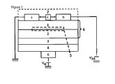
- the devices described in the present finding have a structure of a field effect or similarly of an organic thin film transistor (OFET) as displayed in figure 1 .
- the transistor is fabricated starting from a highly doped silicon substrate (resistivity 0.02-1 Ohm/cm) acting as gate material, It is also possible to use a metallized glass slide of a flexible plastic substrate but also paper or fabric substrate.
- the doped silicon water is covered by a SiO 2 layer (thickness 100 nm or 300 nm) acting as a dielectric.
- the suggested procedures can be readily extended also to other oxides such as TiO 2 or polymeric dielectrics provided that they are properly treated in order to hold -OH type functionalities allowing the anchoring of the biological layer.
- Dielectric thickness and material dielectric constant determine the bias necessary to operate the device.
- bias are as high as -100 V (-40 V for 100 nm thick SiO 2 ) but examples in literature show that OFETs, also used as sensors, can be operated at bias lower than 1 Volt.
- a cleaning step of the dielectric surface is always performed, it includes: washing in H 2 O, followed by washing in acetone and again H 2 O; sonication in isopropanol for 10 minutes; sonication in methanol for 10 minutes; again H 2 O - acetone - H 2 O.
- Bio systems can be covalently bound or otherwise adhered (physical adsorption, spin-coating) to the dielectric.
- An organic semiconductor such as for example oligomers or polymers of thiophene, also substituted with alkyl chains, oligoacenes such as pentacene, tetracene or anthracene, phthalocyanines, porphyrins but even naphthalenes, fullerenes, etc., is deposited on top of the deposited biological layer. Indeed, both p and n organic semiconductors can be used.
- the organic semiconductor can be deposited from a solution (spin-coating or drop-casting), in the case of soluble materials or by thermal evaporation in the case of not soluble materials. In this specific case a p-type organic semiconductor is deposited by spin-coating.
- poly(3-hexylthiophene-2,5-diyl - P3HT) (Sepiolid P 200, supplied by Basf) was dissolved in chloroform at a concentration of 2,6 mg/ml.
- the commercial material was purified following a procedure of subsequent washing in a soxhlet apparatus with methanol and hexane.
- the deposition of purified P3HT was performed by spin-coating at a spin rate of 2000 rpm 30 sec long.
- This patent proposes, for the first time, an OFET comprising a biological layer directly at the interface with the channel region.
- This configuration has the capability to provide an OFET device with better electronic properties and higher performances, particularly in terms of sensitivity, since the recognition event of the analyte takes place where the bidimensional charge transport (field effect) responsible of current, amplification occurs.
- the device structure is shown in figure 1 .
- All the deposited biological layers, as well as all the active multilayers meaning the biological layer covered by the organic semiconductor
- the first operative mode was employed to get general information about the composition and chemical speciation of the surface.
- the ARXPS mode was used as a not destructive study of clement and functional group distribution in a thin layer corresponding to about 5 nm of the most external surface portion.
- ionic controlled erosion ion-beam assisted depth-profiling XPS
- target elements such as phosphorus, sulphur, nitrogen, were chosen to identify the presence of single multilayer component and an advanced XPS data analysis software was subsequently employed to obtain the elicited profiles.
- This method of OFET manufacturing is compatible with screen-printing technologies allowing device realization, even in array configuration, at low cost and allows implementing them on plastic, paper or even fabric substrates.
- the geometry used to define the S and D contacts results in rectangular pads that can he spaced by I to 500 ⁇ m; this spacing is addressed as "L" ( figure 1 ) being the channel length.
- the S and D contacts can be also deposited directly on the dielectric layer just after surface cleaning procedure.
- the device is operated in the common source configuration. Because or the capacitive coupling effect between dielectric and active material (performed by biasing the gate contact respect to the grounded source), it is possible to tune the current passing between source and drain.
- Both the bare P3HT OFET devices as well as the OTFT comprising the multilayer were then exposed to the analyte.
- the transfer characteristics were measured upon exposure of the channel region to the analyte to he detected.
- the transfer characteristics current changes before and after the exposure is taken as the sensor response.
- ad hoc designed control experiments were performed as described in details in the examples reported (vide infra). To perform the sensing experiments, different procedures were used for the detection of volatile and liquid substances.
- a controlled concentration flow of the analyte was obtained by bubbling the inert carrier gas, N 2 , into two bubblers containing the analyte in its liquid form. This allows to obtain a nitrogen flow having a partial pressure of the analyte vapours equal to the pressure of saturated vapour of the same analyte at the working temperature of the analysis. To increase the saturation efficiency, besides the trap, the two bubblers were used in series. The temperature was controlled and kept constant by dipping the bubblers in a cryothermostal. Flow control is achieved through a system of two computer controlled flowmeters (Brooks Smart DMFC model 5850C). The described experimental apparatus, allows to control independently and simultaneously the flow of the carrier gas and that of the nitrogen saturated with the analyte. Analyte concentrations sent on the sample can be changed with subsequent dilutions obtained by changing the rate of the two flows.
- the solution containing the analyte was deposited directly on the organic semiconductor and incubated long enough to allow both the diffusion of analyte through the organic semiconductor layer and the binding with the element deputed to biological recognition. Subsequently, the not bound excess analyte was removed by washing and the device was dried under a nitrogen flow. Examples of realizations of two specific OFET sensors used for different applications are reported in the following:
- the OFET was realized using phospholipids layer as biological system.
- This device is proposed as a sensor for anaesthetics.
- the device sensitivity to anaesthetic substances such as halothane and diethyl-ether resulted an order of magnitude higher than that to other organic vapours, with the same volatility, such as acetone or isopropanol.
- This is particularly interesting also because it is very difficult to selectively detect organic substances with the same volatility by means of a chemical sensor.
- the device was realized as follows. A layer of phospholipids was deposited, on a properly washed and treated SiO 2 surface, by starting from an aqueous suspension of single unilamellar vesicles (SUV). The suspension was realized dissolving 10 mg of soybean lecithin (EPIKURON 200, Cargill) in chloroform allowed to evaporate under vacuum, afterword. The phospholipids were suspended in 1 ml of distilled water and sonicated on ice for 30 minutes. Then, the obtained multilamellar vesicles suspension was repeatedly subjected to extrusion using a polycarbonate filter having pore sizes of 100 nm, to obtain evenly dimensionally distributed unilamellar phospholipidic vesicles.
- SUV single unilamellar vesicles
- P3HT is subsequently deposited again by spin-coating but from chloroform directly on the phospholipidic film as well as on the "purple membranes".
- the measurements reported in figure 2 show that the deposition of the organic semiconductor does not remove the phospholipidic film.
- AFM measurements evidenced in fact that the phospholipidic layer deposited by spin coating from water is not removed when bare chloroform is spun over it. The result of such an experiment is a drastic reduction of thickness which goes down to few nanometer and the surface becomes much more even and extremely flat.
- the comparison between the transfer characteristics of sensor 1 exposed to an inert gas (N 2 ) and to a flow of 40% ethyl-ether in N 2 is outlined in figure 5 .
- the calibration curves of figure 6 evidence how the response to ethyl-ether is about a factor 10 higher for the OFET including the phospholipidic layer respect to the control device. Instead, it is interesting to note that the exposure to acetone vapours does not cause an important effect neither in sensor 1 and nor in the control device. It is also interesting to observe that exposure of the same devices to an alcohol such as isopropanol displayed a similar behaviour to that of acetone.
- a sensor with an organic thin film transistor (OTFT) configuration is particularly suitable to the aim, not only for the already proven high sensitivity, but mostly because it exploits an interface phenomenon, such as the field effect, to induce the electronic response.
- OTFT organic thin film transistor
- the low manufacturing costs and the possibility to miniaturize the devices based on a soluble organic semiconductors are further advantages of the system object of this patent.
- the methods adopted for the realization of sensor 1 can be readily extended to the realization of a sensor comprising the biological system (c) which includes any one of the proteins of which at point (b) or (t).
- the realization procedure of the device foresees the deposition of double phospholipidic layers which includes membrane proteins (such as receptors, ionic channels or enzymes of different kind), starting from proteoliposomes, or better vesicles containing in the double lipid layer the proteins of interest.
- Proteoliposomes are prepared by molecular exclusion chromatography (micelles mixed with phospholipids, detergent and protein in proper ratios, are filtered on Sephadex G-50 columns) and arc subsequently deposited on the dielectric layer or the device.
- the OFET sensor was fabricated using the streptavidin-biotin system as model. Streptavidin was immobilized on the dielectric layer by physical adsorption, spin-coating and chemical binding. The fabrication steps of the biomolecule immobilization on the OTFT sensor surface are reported in the following. The procedures optimized for the specific reported case of streptavidin can he readily extended to OFETs realized with the other protein classes mentioned at point (b) as well as with biological systems reported at points (d) and (e) and from synthetic receptors as reported at point (f).
- Immobilization of streptavidin by physical adsorption was performed incubating the Si/SiO 2 substrates, previously washed and activated, with a streptavidin solution in phosphate buffered saline 0.01M pH 7.4 (PBS) overnight at room temperature. The substrates was then washed with water and saturated with a solution containing BSA 1% in PBS for 2 hours. After washing with water the devices were dried under nitrogen flow and used for the organic semiconductor deposition. Concentrations of streptavidin in the range 1-100 ⁇ g/ml were used to optimize capture protein immobilization.
- Immobilization of streptavidin by spin-coating was achieved by depositing a solution of streptavidin in water on Si/SiO) 2 substrates, previously washed and activated, at a rate of 200 rpm until evaporation of the solvent was complete. Concentrations of streptavidin in the 1-100 ⁇ g/ml range were used to optimize capture protein immobilization. For the streptavidin chemical binding the washed and activated devices were functionalized with a 5% solution of 3-aminoprapyltrictoxysilane (APTES) in ethanol.
- APTES 3-aminoprapyltrictoxysilane
- the functionalized devices were then treated with a 2.5% glutaraldehyde solution in PBS and subsequently, in order to obtain the binding of the protein, they reacted with a streptavidin solution in PBS.
- optimization of capture protein immobilization is performed through luminescence imaging.
- the homogeneity of the immobilized biomolecule layer on sensor surface and the effect of organic solvents such as chloroform, used for deposition of the organic semiconductor on the protein layer, were valued by means of luminescence imaging techniques using the streptavidin - Alcxa Fluor 488 fluorescent conjugate.
- the fluorescence images were acquired using a fluorescence microscope equipped with a CCD camera.
- the devices, on which protein recognition elements were immobilized were subjected first to fluorescence analysis and subsequently Lo treatment with an organic solvent.
- the homogeneity of the deposited protein layer was evaluated by taking fluorescence images acquired for each immobilization procedures and for each concentration. Furthermore, the fluorescence images were acquired before and after treatment with chloroform to evaluate if the treatment with organic solvents (used for the deposition of the organic semiconductor on the biomolecule layer) modifies the structure of the immobilized protein.
- the images obtained by different immobilization techniques show that the best results are obtained immobilizing the protein molecules through the spin-coating technique and chemical binding. In fact, a homogeneous protein layer is obtained with these two techniques and small covering imperfections arc observable only at very high magnifications.
- HMDS hexamethyldisilazane
- a 100 ⁇ g/ml HRP solution in water was deposited by spin-coating on the washed and activated device SiO 2 surface. After enzyme immobilization, the organic semiconductor was deposited and finally the chemiluminescence substrate was added. Chemiluminescence images were immediately acquired by a CCD camera. As a result of the chemiluminescence substrate addition it would be possible to observe a light signal only if the enzyme remains active and if the substrate components reach the immobilized enzyme passing through the semiconductor.
- the chemiluminescence images were recorded on devices, on which HRP was deposited, before and after treatment with chloroform and after deposition of the organic semiconductor. From the images it is possible to observe that in all cases a light signal is visible, clearly indicating that the enzyme remains active and that the analyte, in this case luminol, is able to pass through the organic semiconductor. Further, this response demonstrates that the treatment which is necessary to device preparation keeps HRP enzyme functionality unchanged.
- OFET devices ( figure 1 ) can be employed as biosensors since, as a result of the specific interaction of the analyte with the biological molecules immobilized as previously described, a variation of the electric OTFT properties due to changes which take place in the organic semiconductor deposited on the bioactive material occurs.
- the sensing measurements were performed measuring also in this case the transistor transfer characteristics in the absence and in the presence of the analyte.
- Devices, in which the biological recognition element was not immobilized (then only P3HT), were used as negative control. Before the electric measurements the device was divided into two regions, a region was used as blank, in other words only water was added and a 10 ⁇ g/ml biotin solution in water was distributed on the other region.
- Table 1 The results reported in table 1 show the very lower variability coefficient respect to the negative control, both for the blank and after biotin addition obtained in the case of the device functionalized with the biological recognition element.
- Table 1 In the table the mean values of the ID current calculated from the trans characteristics for VG- 395 after analysis of seven channels of the same device are reported. Further, the corresponding standard deviations (SD) and the percentage coefficients of variability (CV%) are reported.
- Device Mean ( 7) [ D for V 0 -] SD CV% 395 P3HI/water 0.65 ⁇ A 0.07 10% P3HT/biotin 0 39 ⁇ A 0.01 10% STRCP+P3HT/water 0.60 ⁇ A 0.03 5% SIRCP+P3HT/biotin 0.28 ⁇ A 0.0 4%
- bovine serum albumin BSA
- anti-biotin antibodies future developments could be directed even to integrate systems of microfluidics in the device for reagent distribution and to develop multianalyte systems.
- biospecific probes will be immobilized in different positions of the device, and the signals coming from the different points (corresponding to the binding of the specific analyte) will be detected separately. In this way, it will be possible to determine and quantify different analytes which are present on the same sample simultaneously.
- the employed technology will be that of the realization of an OFET array. It is then possible to consider the development of a new platform using the electronic sensors proposed in this patent employing different biological layers also in array (matrix) configuration.
- Such system would allow the detection of a multianalyte system and the manufacturing of these devices could be performed with technologies presently employed for organic electronics on a large scale. This aspect is particularly important in clinical diagnosis and in "Point Of Care" monitoring in fact the devices to be developed could be used for the simultaneous detection of a groups of analytes related to a particular pathology, Further, disposable devices could be realised too, such format will allow to overcome the problem of biosensors regeneration. Furthermore, it will avoid the risk of cross-contamination between different samples and the danger of contamination linked to the handling of infected clinical samples.
Landscapes
- Chemical & Material Sciences (AREA)
- Engineering & Computer Science (AREA)
- Physics & Mathematics (AREA)
- Health & Medical Sciences (AREA)
- Life Sciences & Earth Sciences (AREA)
- Molecular Biology (AREA)
- Spectroscopy & Molecular Physics (AREA)
- Nanotechnology (AREA)
- General Health & Medical Sciences (AREA)
- Biochemistry (AREA)
- Analytical Chemistry (AREA)
- Electrochemistry (AREA)
- Chemical Kinetics & Catalysis (AREA)
- General Physics & Mathematics (AREA)
- Immunology (AREA)
- Pathology (AREA)
- Biophysics (AREA)
- Materials Engineering (AREA)
- Mathematical Physics (AREA)
- Theoretical Computer Science (AREA)
- Crystallography & Structural Chemistry (AREA)
- Microelectronics & Electronic Packaging (AREA)
- Investigating Or Analyzing Materials By The Use Of Electric Means (AREA)
Abstract
Description
- The object of the present invention consists of innovative methods for realizing organic field effect transistors (OFET) comprising layers of sell-assembled biological systems as integral part of the active material. Further, the present invention relates to the use of said OFET as label-free, selective and sensitive sensors for detecting volatile or liquid substances for example of interest in biomedical field.
- Several sectors in analytical chemistry, such as, for instance food analysis, environmental monitoring and clinical diagnostics, displayed a strong interest toward the development of devices to be directly used in on-field applications. For example, the concept of POC (Point Of Care) analysis refers to the possibility to perform diagnostic procedures, in an accurate and rapid way, directly in the place where they are needed (doctor's office, private hospital). Of course, the analytical systems for such applications must be easy to use and provide easily readable outputs/responses and quantitative data. In this regard, biosensors being capable to perform fast analysis and label-free detection, have been proven to be very promising since they are able to directly probe a biological recognition event without the need of a marker. Recently, attention was directed to the development of immunosensors and genosensors offering a fast, continuous and in situ detection as well as a quantification of analytes in complex matrices such as blood. Such biosensors exploit specific immunologic (antigen/antibody binding) or nucleic acid hybridization (binding of complementary sequences) reactions for identification and quantification of analytes, using a proper transduction signal which can be an optical, electrochemical, or electronic one. In particular, immunosensors, in comparison to other analytical methods, present the following advantages: they are selective and sensitive, they can be used for on field analysis, they can be fully automated, the response can he fast and the analytes do not need to be purified or treated before the analysis. However, a lot of presently developed biosensors present several disadvantages in terms of cost, reagents availability, regeneration and reproducibility. Moreover, the sensor sensitivity is markedly influenced by the transduction mechanism and, today, only few satisfactory performing biosensors are available on the market. Hence, the need arises to have fast, reliable, accurate, portable and low cost biosensors.
- Although presently only some preliminary studies have been performed, OFETs present interesting characteristics to be successfully employed as label-free biosensors. The OFET sensor field has been rising a great attention in the last decade. This is mostly due to the possibility to implement such devices in high performance portable detection systems. One of the sensor market" major request is the possibility to have devices capable of detecting, biological and chemical analytes, on-line and in situ. Such devices can be employed in a wide range of applications ranging from food and beverage control, to medical diagnostic and public security. Such requirements are not still completely fulfilled by the technology supporting the sensors currently on the market. The selectivity, the capability to work at room temperature and the high sensitivity to a wide range of analytes are still open questions in the field and, in this respect, OFETs have shown the capability to overcome some of these limits. As a matter of fact they behave as multi-parameter sensors, display a high repeatability, a fast and reversible response, can work at room temperature, display a good selectivity toward a wide range of analytes, and allow on-state analyte detection and amplified sensitivity as the applied gate bias is increased. Furthermore, the bilayer architecture OFET sensor, recently proposed, appears to be of great interest for high performance analysis of chiral analytes. The bilayer structure has been engineered combining field effect transistors with chiral recognition properties, allowing a differential enantiomeric detection of volatile analytes at unprecedented low concentration, namely in the ppm range. Biological recognition measurements are usually performed in aqueous media and low voltage transistors are able to assure stable working conditions in such an environment. Water electrolysis and high ionic analyte conductivity represent, indeed, the main drawbacks to overcome for applications in an aqueous environment. New organic and inorganic dielectrics have been recently developed to lower OFET threshold bias and 10 invert the slope below the threshold voltage, both responsible for the high OFET voltages. Such figures of merit depend also on gate dielectric properties. This implies the development of high capacity thin gate dielectrics, one of the main challenges of organic electronics. The immobilization of biomolecules, such as DNA, enzymes or other proteins, on sensor surface represents a new basic research area involving different interdisciplinary fields. The development of new structures which arc capable to provide a direct link between the complex world of biology and digital electronics is a target of scientific research worldwide. The choice of the method of bioprobe immobilization allowing a specific biomolecule to retain its biological function is one of the most important aspects in biosensor fabrication. To obtain a biorecognition reaction which is selective, sensitive and reproducible, it is necessary to immobilize the biomolecules on the surface to obtain well oriented molecular layers. Further, to increase sensitivity it is essential to reduce the distance between the transduction surface and the layer of immobilized biomolecules. The biomolecules can be immobilized on a sensor surface in different ways. For immobilization purpose, several materials can be used such as for instance nafion, sol-gel, lipid membranes, conductive polymers or self-assembled monolayers (SAMs). SAMs are particularly suitable as biosensor active layer since they form thin, ordered and stable monolayers and they can be grated on the surface thanks to the wide headgroup availability. Further they can provide to biomolecules a microenvironment similar to that of the membranes and require only minimal quantities of often very expensive biomolecules. Another alternative method consists in the use of electrosynthesized conductive polymers as matrices for immobilizing biocomponents. From the scientific literature and in particular as a consequence of the important work of the rescarchers Foulds and Lowe published in 1988, the immobilization of biomolecules such as enzymes, DNA, antibodies and even whole cells in conductive polymers was studied for manufacturing biosensors, including immunosensors. Among all conductive polymers studied to date, polypyrrole (PPy) can be considered one of the most interesting materials for its excellent conductivity, stability and biocompatibility even at neutral pH. In addition to PPy and its derivatives the use of conductive polymers such as poly(aniline), poly(3-hexylthiophene), poly(o-amil1obenzoic acid) has been studied for the realization of immunosensors. Recently attention has been directed to the use of systems mimicking cell membranes for immobilizing biomolecules. The low bioactivity of membranes renders them particularly interesting as an interface between the not biological material on sensor surface and the biologically active fluids. Lipid membranes represent also a natural environment for biological molecules. Thanks to the natural environment, it is possible to prevent biomolecule denaturation and to obtain high sensitivity and selectivity. Furthermore, low membrane bioactivity prevents signal interferences, while active biomolecule localization on a surface favours signal transduction. The membranes can be deposited on surface in several ways. In particular, sensor surface can be modified introducing binding sites specific for lipid molecules in order to deposit steadily the membranes. The configuration of the devices to be developed combines high selectivity of bio-recognition with the high sensitivity typical of the electronic transduction offering high analytical performances. Such devices do not require large sample volumes or toxic solvents for the analysis, they are characterized by minimal sample pretreatment and low reagent consumption, present high specificity, in the analysis of complex matrices too, and can be readily miniaturized and automatized in portable and disposable devices.
- Furthermore, configurations of devices presenting a layer of a biological recognition system between the dielectric and the organic semiconductor, which represents the peculiarity and the innovation of this specific patent, have never been proposed before.
- All devices object of the present invention can function as electronic sensors and can be realized by techniques developed in the framework of organic electronics. The main advantages are:
- OFET sensors allow label-free detection; in fact it is not necessary to label the sample by attaching fluorescent or electroactive markers to the species to be analyzed;
- single devices, as well as matrix systems (array), arc miniaturizable and realizable with low cost screen-printing technologies and on substrates made of plastic, paper or even Fabrics;
- they do not need a reference electrode to measure the current changes induced by the interaction with the species to he detected.
- Currently available sensors for the suggested detections, for example those with optical or electrochemical detection, fail to fulfil at least one of the above listed characteristics.
- These and other advantages will be better highlighted in the detailed description of the invention which specifically refers to tables 1/4,
figures 1 to 8 , in which an example absolutely not limiting of a preferred realization of the present finding is exposed. In particular: -
figure 1 shows the OFET sensor structure made of an active material comprising a biological layer of type (a), (b), (c), (d) or (e), as reported in detail at page 11, covered by an organic semiconductor, for example poly-3-hexyl-thiophene (P3HT); in the figure the organic semiconductor OS (1), the self-assembled biological layer SBL (2), the dielectric (3), the conductive substrate (4), the channel region (5), the active material (6) and the analyte (7) are displayed; -
figure 2 shows the curve of the micro-luminescence spectra of a phospholipidic layer, properly labelled with Texas-Red fluorophore, the P3HT and the multilayer made of phospholipids on which P3HT was deposited. Both the phospholipidic and the P3HT layer were deposited by spin-coating; -
figure 3 shows: (a) the curves of the current-voltage characteristics (IDS vs. VDS at different VG values) of a P3HT OFET; (b) transfer characteristics of the same device (IDS vs. VG at VDS =-30 V); -
figure 4 shows the curves of current- voltage characteristics of an OFET made of a phospholipidic layer covered by a P3IIT layer; -
figure 5 shows the transfer characteristics curves ofsensor 1 exposed to an inert gas (N2) atmosphere and to ethyl-ether. Sensor response is defined by the difference between IDS values (measured in N2 and in the analyte atmosphere) at a fixed VG potential; -
figure 6 shows the graph of the calibration curve ofsensor 1 and the control device (P3IIT OFET) exposed to a controlled atmosphere of ethyl-ether or acetone. Each data point is the result of three measurements and the error bars are the mean standard errors; -
figure 7 shows the transfer characteristics curves obtained for OFET functionalized with streptavidin exposed to water (solid line curve - streptavidin + P3HT / H2O), OFET functionalized with streptavidin exposed to biotin (short dashed line curve - streptavidin + P3HT / biotin). Dotted and long dashed line curves are referred to the two negative control experiments. - The devices described in the present finding have a structure of a field effect or similarly of an organic thin film transistor (OFET) as displayed in
figure 1 . The transistor is fabricated starting from a highly doped silicon substrate (resistivity 0.02-1 Ohm/cm) acting as gate material, It is also possible to use a metallized glass slide of a flexible plastic substrate but also paper or fabric substrate. In the present case the doped silicon water is covered by a SiO2 layer (thickness 100 nm or 300 nm) acting as a dielectric. The suggested procedures can be readily extended also to other oxides such as TiO2 or polymeric dielectrics provided that they are properly treated in order to hold -OH type functionalities allowing the anchoring of the biological layer. Dielectric thickness and material dielectric constant determine the bias necessary to operate the device. In the exposed case bias are as high as -100 V (-40 V for 100 nm thick SiO2) but examples in literature show that OFETs, also used as sensors, can be operated at bias lower than 1 Volt. Before device fabrication, a cleaning step of the dielectric surface is always performed, it includes: washing in H2O, followed by washing in acetone and again H2O; sonication in isopropanol for 10 minutes; sonication in methanol for 10 minutes; again H2O - acetone - H2O. It is generally convenient to perform a washing treatment with solvents at increasing polarity and even a treatment with oxygen plasma followed by an activation step of the oxide, aimed at increasing the number of polar groups (-OH) on substrate surface. This last step is performed using a solution composed of sulphuric acid and hydrogen peroxide (piranha) or UV treatment with ozone. The innovative aspects of the device, object of the present patent is the presence of a biological layer deposited directly on the dielectric surface. The possible biological systems include: - (a) single or double phospholipidic layers;
- (b) layers composed by proteins such as: receptors, antibodies, ionic channels and enzymes;
- (c) single or double phospholipidic layers with inclusion or anchoring of the proteins listed at point (b);
- (d) layers composed by oligonucleotide (DNA, RNA, PNA) probes;
- (e) layers composed by cells or viruses;
- (f) layers composed by synthetic receptors (molecules or macromolecules similar to biological receptors for properties, reactivity or steric aspects).
- Biological systems can be covalently bound or otherwise adhered (physical adsorption, spin-coating) to the dielectric.
- An organic semiconductor, such as for example oligomers or polymers of thiophene, also substituted with alkyl chains, oligoacenes such as pentacene, tetracene or anthracene, phthalocyanines, porphyrins but even naphthalenes, fullerenes, etc., is deposited on top of the deposited biological layer. Indeed, both p and n organic semiconductors can be used. The organic semiconductor can be deposited from a solution (spin-coating or drop-casting), in the case of soluble materials or by thermal evaporation in the case of not soluble materials. In this specific case a p-type organic semiconductor is deposited by spin-coating. Specifically the poly(3-hexylthiophene-2,5-diyl - P3HT) (
Sepiolid P 200, supplied by Basf) was dissolved in chloroform at a concentration of 2,6 mg/ml. The commercial material was purified following a procedure of subsequent washing in a soxhlet apparatus with methanol and hexane. The deposition of purified P3HT was performed by spin-coating at a spin rate of 2000rpm 30 sec long. - This patent proposes, for the first time, an OFET comprising a biological layer directly at the interface with the channel region. This configuration has the capability to provide an OFET device with better electronic properties and higher performances, particularly in terms of sensitivity, since the recognition event of the analyte takes place where the bidimensional charge transport (field effect) responsible of current, amplification occurs. The device structure is shown in
figure 1 . All the deposited biological layers, as well as all the active multilayers (meaning the biological layer covered by the organic semiconductor), underwent an extensive surface and volume spectroscopic characterization. Surface characterization was performed through X rays photoelectronic spectroscopy (XPS), used in conventional, angle resolved (ARXPS), and imaging (map-scan XPS) mode. The first operative mode was employed to get general information about the composition and chemical speciation of the surface. The ARXPS mode was used as a not destructive study of clement and functional group distribution in a thin layer corresponding to about 5 nm of the most external surface portion. Further, ionic controlled erosion (ion-beam assisted depth-profiling XPS) was adopted to explore layers of higher thickness. In both cases for the reconstruction of the concentration profiles, target elements, such as phosphorus, sulphur, nitrogen, were chosen to identify the presence of single multilayer component and an advanced XPS data analysis software was subsequently employed to obtain the elicited profiles. Finally, the analysis performed in imaging-XPS mode with a resolution corresponding to about 20 µm, allowed to verify the uniformity of the multilayers surface. Volume characterization was performed too by micro-luminescence technique on both the single P3HT and on the multilayers. As an example the case of the sample including the phospholipidic layer is reported.Figure 2 shows the luminescence spectra excited with the 476 nm line of a Kripton laser. - In such
figure 2 the micro-luminescence spectra of just the phospholipids film deposited through spin-coating from an aqueous solution (further details are reported in the section dedicated to example I) are compared; this spectrum is particularly intense since fluorophore (Texas-Red) labelled phospholipids have been used. A luminescence signal can be recorded also for the bare P3HT film, even though less intense and red shifted. The characterization proceeded with the measurement of a sample fabricated by depositing the phospholipidic layer covered by a P3HT layer. This latter layer was deposited by spin-coating from a chloroform solution (example 1). It is evident that the luminescence line shape of the phospholipidic layer covered by the organic semiconductor, shows contributions from both the phospholipid and the organic semiconductor staking layers. This confirms that P3HT deposition does not remove the biological layer deposited underneath. This is a critical information that supports the interpretation of the results, shown in the following, obtained using this system as a sensor. The structure was confirmed also by morphological measurements performed by atomic force scanning microscope. Manufacturing of OFET device was then completed by depositing the source (S), drain (D) and gate (G) contacts by thermal evaporation (8 x 10⁻⁷ torr) of gold through a shadow mask. This method of OFET manufacturing is compatible with screen-printing technologies allowing device realization, even in array configuration, at low cost and allows implementing them on plastic, paper or even fabric substrates. The geometry used to define the S and D contacts results in rectangular pads that can he spaced by I to 500 µm; this spacing is addressed as "L" (figure 1 ) being the channel length. The S and D contacts can be also deposited directly on the dielectric layer just after surface cleaning procedure. The device is operated in the common source configuration. Because or the capacitive coupling effect between dielectric and active material (performed by biasing the gate contact respect to the grounded source), it is possible to tune the current passing between source and drain. The charge induced by the gate field is confined, because of field effect, to a bidimensional region, called in fact the channel region, at the interface with the dielectric. OFET devices, including a biological active layers as reported infigure 1 , were used as sensors by first measuring the electrical behaviour of the device composed by the P3ITT film only. Typical current voltage characteristics (I-V) are reported infigure 3 . In particularfigures 3(a) shows the I-V characteristics obtained measuring the IDS current flowing between S and D as a function of the VDS bias at different gate biases, VG. Infigure 3(b) the IDS current curves as a function of VG bias at constant VDS (-40 V) are reported. Such curves are called transfer characteristics. The data analysis, performed according to consolidated procedures results for the device infigure 3 in a field effect mobility, µFET, of 5x10⁻³ cm2/Vs, Ion/Ioff- 10, and threshold voltage, Vt, of 7 V. - The current-voltage characteristics of an OFET, fabricated depositing a P3ITT layer on top of a phospholipidic layer as previously described are reported in
figure 4 . It is interesting to note that also the device including the phospholipid layer covered by the P3HT films works beautifully as transistor. In particular, µFET, of 6.25x 10⁻³ cm2/Vs, Ion/Ioff = 100, which is in line with the best performing P3HT devices. Even more striking is the fact that figure of merits such as the amplification ratio (Ion/Ioff), even improved with the introduction of the phospholipidic layer. It is the first time that an OFET comprising a biological layer at the interface between the organic semiconductor and the gate dielectric is realized and proven to work at such high level of performances. In this case the electronic characteristics are even better for the OFET comprising the biological layer. - Both the bare P3HT OFET devices as well as the OTFT comprising the multilayer (including the biological layer as in
figure 1 ) were then exposed to the analyte. For both devices the transfer characteristics were measured upon exposure of the channel region to the analyte to he detected. The transfer characteristics current changes before and after the exposure is taken as the sensor response. Furthermore, ad hoc designed control experiments (blank measurements) were performed as described in details in the examples reported (vide infra). To perform the sensing experiments, different procedures were used for the detection of volatile and liquid substances. - A controlled concentration flow of the analyte was obtained by bubbling the inert carrier gas, N2, into two bubblers containing the analyte in its liquid form. This allows to obtain a nitrogen flow having a partial pressure of the analyte vapours equal to the pressure of saturated vapour of the same analyte at the working temperature of the analysis. To increase the saturation efficiency, besides the trap, the two bubblers were used in series. The temperature was controlled and kept constant by dipping the bubblers in a cryothermostal. Flow control is achieved through a system of two computer controlled flowmeters (Brooks Smart DMFC model 5850C). The described experimental apparatus, allows to control independently and simultaneously the flow of the carrier gas and that of the nitrogen saturated with the analyte. Analyte concentrations sent on the sample can be changed with subsequent dilutions obtained by changing the rate of the two flows.
- To perform the bio-sensing measurements in water, the solution containing the analyte was deposited directly on the organic semiconductor and incubated long enough to allow both the diffusion of analyte through the organic semiconductor layer and the binding with the element deputed to biological recognition. Subsequently, the not bound excess analyte was removed by washing and the device was dried under a nitrogen flow. Examples of realizations of two specific OFET sensors used for different applications are reported in the following:
- In this case, the OFET was realized using phospholipids layer as biological system. This device is proposed as a sensor for anaesthetics. The device sensitivity to anaesthetic substances such as halothane and diethyl-ether resulted an order of magnitude higher than that to other organic vapours, with the same volatility, such as acetone or isopropanol. This is particularly interesting also because it is very difficult to selectively detect organic substances with the same volatility by means of a chemical sensor.
- The device was realized as follows. A layer of phospholipids was deposited, on a properly washed and treated SiO2 surface, by starting from an aqueous suspension of single unilamellar vesicles (SUV). The suspension was realized dissolving 10 mg of soybean lecithin (
EPIKURON 200, Cargill) in chloroform allowed to evaporate under vacuum, afterword. The phospholipids were suspended in 1 ml of distilled water and sonicated on ice for 30 minutes. Then, the obtained multilamellar vesicles suspension was repeatedly subjected to extrusion using a polycarbonate filter having pore sizes of 100 nm, to obtain evenly dimensionally distributed unilamellar phospholipidic vesicles. 50 µl of this solution were deposited on the Si/SiO2 substrate, subjected then to a rotation of 200 rpm for twenty minutes. Similarly but on a different device, also a film known as "purple membranes" constituted by the bacteriorhodopsin membrane protcin and lipids was deposited. Even in this case, the deposition was performed by spin-coating from a "purple membranes" suspension in H2O. Atomic force scanning micrographies (AFM) show how such spin coating procedure at a very slow rotation results in a multilayer of phospholipids made of flat surfaces with a very smooth and even surface. P3HT is subsequently deposited again by spin-coating but from chloroform directly on the phospholipidic film as well as on the "purple membranes". The measurements reported infigure 2 show that the deposition of the organic semiconductor does not remove the phospholipidic film. AFM measurements evidenced in fact that the phospholipidic layer deposited by spin coating from water is not removed when bare chloroform is spun over it. The result of such an experiment is a drastic reduction of thickness which goes down to few nanometer and the surface becomes much more even and extremely flat. The comparison between the transfer characteristics ofsensor 1 exposed to an inert gas (N2) and to a flow of 40% ethyl-ether in N2 is outlined infigure 5 . It is evident that ethyl-ether causes a remarkable decrease of the current flowing in the channel region. Similar results were obtained with an anaesthetic still in use such as halothane. In this case the measured responses are in the range of clinical concentrations (2-4 % in N2) useful for real applications. An even higher and opposite sign response was obtained substituting the simple phospholipidic layer with a "purple membranes" which is known to contain in addition to phospholipids also bacteriorhodopsin. In fact, in this case the exposure to the anaesthetic causes a current increment. Being P3HT a p-type semiconductor the current increment is to be ascribed to the injection of H' ions in the bidimensional transport region of the transistor, as it is foreseen by the conformational change of bacteriorhodopsin. This result is particularly remarkable since it demonstrates how it is possible to integrate a membrane protein in an OFET to build a sensor. But it is even more important that the protein continues to work and the transistor allows performing an electronic detection of a conformational change. The calibration curves ofsensor 1, containing just the phospholipidic layer, when exposed to both ethyl-ether and another organic vapour of comparable volatility (acetone) are shown infigure 6 . The response ΔI reported on the abscissa is the change of IDS following the exposure to the analytes vapours respect to the value in N2. Both values are taken at VG = -40 V. For comparison, an OFET with only P3HT was exposed to the same substances. The calibration curves offigure 6 evidence how the response to ethyl-ether is about afactor 10 higher for the OFET including the phospholipidic layer respect to the control device. Instead, it is interesting to note that the exposure to acetone vapours does not cause an important effect neither insensor 1 and nor in the control device. It is also interesting to observe that exposure of the same devices to an alcohol such as isopropanol displayed a similar behaviour to that of acetone. The response of the P3HT OFET to isopropanol is slightly higher than foreseen probably because of the swelling effect of the organic semiconductor favoured by interactions between the alkyl chains. A similar effect has been already proven in the past. The mechanisms by which molecules such as ether, balothane, desflurane or nitrogen protoxide, are able of induce a state of general anaesthesia arc not, as yet, fully understood. One of the most accredited theories however foreseen the involvement of just the interactions between the anaesthetic molecules and cell membranes even if it is not clear if the presence of any specific receptors is required. Although these studies evidence the peculiarity of the interactions between anaesthetics and membranes, it was never thought before to employ a phospholipidic bilayer as an active material in a sensor for such substances. A sensor with an organic thin film transistor (OTFT) configuration is particularly suitable to the aim, not only for the already proven high sensitivity, but mostly because it exploits an interface phenomenon, such as the field effect, to induce the electronic response. The synergic effect of these two factors, coupled for the first time in a sensor, generates a device potentially useful for monitoring anaesthetic substances with an interesting degree of selectivity, good sensitivity and excellent reproducibility. The low manufacturing costs and the possibility to miniaturize the devices based on a soluble organic semiconductors are further advantages of the system object of this patent. The methods adopted for the realization ofsensor 1 can be readily extended to the realization of a sensor comprising the biological system (c) which includes any one of the proteins of which at point (b) or (t). The realization procedure of the device foresees the deposition of double phospholipidic layers which includes membrane proteins (such as receptors, ionic channels or enzymes of different kind), starting from proteoliposomes, or better vesicles containing in the double lipid layer the proteins of interest. Proteoliposomes are prepared by molecular exclusion chromatography (micelles mixed with phospholipids, detergent and protein in proper ratios, are filtered on Sephadex G-50 columns) and arc subsequently deposited on the dielectric layer or the device. It is widely reported in literature that, after deposition on a solid substrate, spontaneous melting of the vesicles occurs simultaneously to adsorption of the double layer on the substrate. The case or "purple membranes" previously discussed is only one of the possibly examples. In presence of soluble proteins such as antibodies the deposition strategy foresees anchoring of the protein to a double lipid layer deposited as previously described. But in this case, lipids functionalized with amino or carboxylic groups to which the antibody can be covalently bound through bioconjugation procedures reported in literature and employing the EDC / Sulpho-NHS system have to be used. - In this case the OFET sensor was fabricated using the streptavidin-biotin system as model. Streptavidin was immobilized on the dielectric layer by physical adsorption, spin-coating and chemical binding. The fabrication steps of the biomolecule immobilization on the OTFT sensor surface are reported in the following. The procedures optimized for the specific reported case of streptavidin can he readily extended to OFETs realized with the other protein classes mentioned at point (b) as well as with biological systems reported at points (d) and (e) and from synthetic receptors as reported at point (f). Immobilization of streptavidin by physical adsorption was performed incubating the Si/SiO2 substrates, previously washed and activated, with a streptavidin solution in phosphate buffered saline 0.01M pH 7.4 (PBS) overnight at room temperature. The substrates was then washed with water and saturated with a
solution containing BSA 1% in PBS for 2 hours. After washing with water the devices were dried under nitrogen flow and used for the organic semiconductor deposition. Concentrations of streptavidin in the range 1-100 µg/ml were used to optimize capture protein immobilization. Immobilization of streptavidin by spin-coating was achieved by depositing a solution of streptavidin in water on Si/SiO)2 substrates, previously washed and activated, at a rate of 200 rpm until evaporation of the solvent was complete. Concentrations of streptavidin in the 1-100 µg/ml range were used to optimize capture protein immobilization. For the streptavidin chemical binding the washed and activated devices were functionalized with a 5% solution of 3-aminoprapyltrictoxysilane (APTES) in ethanol. The functionalized devices were then treated with a 2.5% glutaraldehyde solution in PBS and subsequently, in order to obtain the binding of the protein, they reacted with a streptavidin solution in PBS. Next, optimization of capture protein immobilization is performed through luminescence imaging. The homogeneity of the immobilized biomolecule layer on sensor surface and the effect of organic solvents such as chloroform, used for deposition of the organic semiconductor on the protein layer, were valued by means of luminescence imaging techniques using the streptavidin - Alcxa Fluor 488 fluorescent conjugate. The fluorescence images were acquired using a fluorescence microscope equipped with a CCD camera. The devices, on which protein recognition elements were immobilized, were subjected first to fluorescence analysis and subsequently Lo treatment with an organic solvent. The homogeneity of the deposited protein layer was evaluated by taking fluorescence images acquired for each immobilization procedures and for each concentration. Furthermore, the fluorescence images were acquired before and after treatment with chloroform to evaluate if the treatment with organic solvents (used for the deposition of the organic semiconductor on the biomolecule layer) modifies the structure of the immobilized protein. The images obtained by different immobilization techniques show that the best results are obtained immobilizing the protein molecules through the spin-coating technique and chemical binding. In fact, a homogeneous protein layer is obtained with these two techniques and small covering imperfections arc observable only at very high magnifications. Instead, in the case of immobilization by physical adsorption some inhomogeneous areas and dielectric portions not covered by the protein layer can he observed, even at low magnifications. Such observations were also confirmed by electric measurements, in fact, the devices obtained by physical adsorption of the protein exhibited worse electric parameters. Concerning the protein concentration, in all cases, the best results were obtained using a concentration of 10 µg/ml. Such concentration is enough to assure an excess of capture protein so that all antigen molecules can react. Furthermore, working in excess of capture reagent assures that significant signal changes are not observed even in the case of small changes of protein immobilization efficiency. Furthermore, it must be pointed out that a fundamental aspect in the deposition of protein molecules is the dielectric layer hydrophilicity. Tests performed on devices not activated or made hydrophobic by treatment with hexamethyldisilazane (HMDS) showed an insufficient and inhomogeneous deposition of the protein layer. For all protein deposition methods, the fluorescence images obtained after treatment with chloroform highlighted that treatment with the organic solvent does not change the structure of the immobilized protein layer. - Analyte capability to pass through the layer of deposited organic semiconductor on the biological recognition element as well as the immobilized protein keeping its biological functionality were devalued by chemiluminescence reinforced by immobilizing the horseradish peroxidase enzyme (HRP) and the chemiluminescence system constituted by luminol/H2O2/p-indophenol. The choice of the chemiluminescence technique was driven by the fact that luminol has a size comparable to that of biotin, then the development of light can be obtained only if this, or the other components of the substrate, pass through the organic semiconductor layer and if the HRP enzyme remains active. To perform the determination, a 100 µg/ml HRP solution in water was deposited by spin-coating on the washed and activated device SiO2 surface. After enzyme immobilization, the organic semiconductor was deposited and finally the chemiluminescence substrate was added. Chemiluminescence images were immediately acquired by a CCD camera. As a result of the chemiluminescence substrate addition it would be possible to observe a light signal only if the enzyme remains active and if the substrate components reach the immobilized enzyme passing through the semiconductor.
- The chemiluminescence images were recorded on devices, on which HRP was deposited, before and after treatment with chloroform and after deposition of the organic semiconductor. From the images it is possible to observe that in all cases a light signal is visible, clearly indicating that the enzyme remains active and that the analyte, in this case luminol, is able to pass through the organic semiconductor. Further, this response demonstrates that the treatment which is necessary to device preparation keeps HRP enzyme functionality unchanged.
- OFET devices (
figure 1 ) can be employed as biosensors since, as a result of the specific interaction of the analyte with the biological molecules immobilized as previously described, a variation of the electric OTFT properties due to changes which take place in the organic semiconductor deposited on the bioactive material occurs. The sensing measurements were performed measuring also in this case the transistor transfer characteristics in the absence and in the presence of the analyte. Devices, in which the biological recognition element was not immobilized (then only P3HT), were used as negative control. Before the electric measurements the device was divided into two regions, a region was used as blank, in other words only water was added and a 10 µg/ml biotin solution in water was distributed on the other region. The transfer characteristics obtained for OFETs functionalized with streptavidin treated only with water, OFETs functionalized with streptavidin following the addition of biotin are displayed infigure 7 . The other curves are measured on the negative control samples where the capture protein is not present. Streptavidin immobilization was always performed by spin-coating. The obtained results show how a much more evident current reduction is achieved in the positive sample respect to the negative one as a result of biotin addition (figure 7 ) Current reduction observed for the negative sample as a result of biotin addition can be ascribed to a weak unspecific interaction of the latter with the organic semiconductor. Anyway, properly optimized saturation procedures can be able to reduce such phenomenon. Seven different OFETs which are present on the same chip were tested to evaluate the intra-device variability. The results reported in table 1 show the very lower variability coefficient respect to the negative control, both for the blank and after biotin addition obtained in the case of the device functionalized with the biological recognition element.Table 1. In the table the mean values of the ID current calculated from the trans characteristics for VG- 395 after analysis of seven channels of the same device are reported. Further, the corresponding standard deviations (SD) and the percentage coefficients of variability (CV%) are reported. Device Mean (= 7) [D for V0 -] SD CV% 395 P3HI/water 0.65µA 0.07 10% P3HT/ biotin 0 39 µA 0.01 10% STRCP+P3HT/water 0.60 µA 0.03 5% SIRCP+P3HT/biotin 0.28µA 0.0 4% - Such result is of noteworthy importance since it highlights how a significant improvement of sensor reproducibility occurs in presence of a specific recognition reaction. Further experiments on a high number of devices could evidence such result even with regard to the inter-device variability. Another parameter that can be used to determine the presence of the analyte is the threshold voltage Vt in fact, values of 32.5 and 16.8 Volt respectively were obtained calculating the mean value of Vt in absence and presence of the analyte, for the different channels subjected to electric testing on a device in which streptavidin was immobilized. Instead, significant changes of Vt are not observed in the negative control. Such result could be explained considering that a change in the charge trapping properties of the OFET biosensor occurs in presence of the streptavidin-biotin complex. From the discussed preliminary results it is possible to understand how the developed biosensor is perfectly capable to discriminate the presence or not of the analyte. Further, from the calibration curve it is possible to determine the concentration of the analyte which is present in the sample too. The advantages of such a device, respect to other commercially available systems, are noteworthy. In fact, beyond the possibility to develop label-free immunosensors or genosensors, namely without the employment of luminescent or enzymatic tracers, the system coupling charge transport through field effect with the bio-sensing process allows to obtain high performances mainly in terms of sensitivity and bias control. Further, the response of these devices is electronic and then immediately available through a proper circuit. Beyond testing the already developed devices using different proteins as negative and positive control, for example bovine serum albumin (BSA) and anti-biotin antibodies, future developments could be directed even to integrate systems of microfluidics in the device for reagent distribution and to develop multianalyte systems. In this last case biospecific probes will be immobilized in different positions of the device, and the signals coming from the different points (corresponding to the binding of the specific analyte) will be detected separately. In this way, it will be possible to determine and quantify different analytes which are present on the same sample simultaneously. The employed technology will be that of the realization of an OFET array. It is then possible to consider the development of a new platform using the electronic sensors proposed in this patent employing different biological layers also in array (matrix) configuration. Such system would allow the detection of a multianalyte system and the manufacturing of these devices could be performed with technologies presently employed for organic electronics on a large scale. This aspect is particularly important in clinical diagnosis and in "Point Of Care" monitoring in fact the devices to be developed could be used for the simultaneous detection of a groups of analytes related to a particular pathology, Further, disposable devices could be realised too, such format will allow to overcome the problem of biosensors regeneration. Furthermore, it will avoid the risk of cross-contamination between different samples and the danger of contamination linked to the handling of infected clinical samples.
- The methods for OFET sensors realization with other proteins classes mentioned at point (b) as well as with the biological systems of which at points (d), (e) or (f) arc depicted in
scheme 1.

- The produced experimental evidences demonstrate that:
- Sensor 1: the OFET employing the layer (a) displays field effect and can work as a sensor of anaesthetics. The methods adopted for the realization of
sensor 1 are readily extendible to the realization of a sensor comprising the biological system (c) which includes anyone of the proteins listed at point (b) or (f). - Sensor 2: the sensor employing a layer with one of the proteins listed at point (b), in particular streptavidin, displays current amplification and works as a sensor of biotin. The methods adopted for the realization of
sensor 2 are readily extendible to OFETs realized with the other protein classes mentioned at point (b) as well as with the biological systems described at points (d), (e) or (f). - Both sensors can provide performances in line with the requirements of possible industrial applications.
Claims (14)
- transistor comprising at least one conductive layer, at least one dielectric layer and at least one thin organic semiconductor film and characterized by at least one layer of biological material deposited directly on the surface of the dielectric.
- Transistor according to claim 1, in which said transistor is an organic field effect or thin film transistor (OFET).
- Transistor according to claim 1 or 2, in which said layer of biological material is constituted by:single or double layers of phospholipids;- layers made of proteins such as: receptors, antibodies, ionic channels and enzymes;- single or double layers of phospholipids with inclusion or anchoring of protein such as: receptors, antibodies, ionic channels and enzymes,- layers made of oligonucleotide (DNA, RNA, PNA) probes;- layers made of cells or viruses;- layers made of synthetic receptors for example molecules or macromolecules similar to biological receptors for properties, reactivity or steric aspects.
- Transistor according to one of claims 1 to 3, in which said layer of biological material is covalently bound or attached, by physical adsorption or by means of other bindings and/or weak forces, or spin-coating to the dielectric.
- Transistor according one of the preceding claims, in which said layer of biological material is covered by an organic semiconductor of type "p" or "n".
- transistor according to one or the preceding claims in which said organic semiconductor is P3HT.
- Transistor according to one of the preceding claims in which said organic semiconductor is deposited by spin-coating or drop-casting in case of soluble materials or by thermal evaporation in case of not soluble materials.
- Transistor according to one of the preceding claims wherein deposition of source (S) and drain (D) and gate (G) contacts occurs by thermal evaporation of gold through a shadow mask or the contacts are deposited by photolithography techniques.
- Transistor according to one of the preceding claims in which the space in between the S and D contacts is comprised between 1 µm and 500 µm.
- A sensor comprising a transistor according to one of the preceding claims in which analyte recognition occurs in the region of bidimensional charge transport, where the field effect. which is responsible of current amplification is established.
- Process for deposition of the elements of biological recognition by multilayer structures comprising the steps of:- activation of oxide by treatment aimed at increasing hydrophilicity;- functionalization of surface;- activation of functional groups;- immobilization of biological preparation.
- Process according to claim 11 in which said step of immobilization is by physical adsorption or by other bindings or weak forces.
- Process according to claim 11 in which said step of immobilization is by spin-coating.
- Process according to claim 11 in which said step of immobilization is by chemical binding.
Priority Applications (1)
| Application Number | Priority Date | Filing Date | Title |
|---|---|---|---|
| EP10425146.7A EP2385563B1 (en) | 2010-05-03 | 2010-05-03 | Organic field effect transistors based on multilayers of self-assembled biological systems covered by an organic semiconductor layer and sensor thereof. |
Applications Claiming Priority (1)
| Application Number | Priority Date | Filing Date | Title |
|---|---|---|---|
| EP10425146.7A EP2385563B1 (en) | 2010-05-03 | 2010-05-03 | Organic field effect transistors based on multilayers of self-assembled biological systems covered by an organic semiconductor layer and sensor thereof. |
Publications (2)
| Publication Number | Publication Date |
|---|---|
| EP2385563A1 true EP2385563A1 (en) | 2011-11-09 |
| EP2385563B1 EP2385563B1 (en) | 2016-11-02 |
Family
ID=43501114
Family Applications (1)
| Application Number | Title | Priority Date | Filing Date |
|---|---|---|---|
| EP10425146.7A Not-in-force EP2385563B1 (en) | 2010-05-03 | 2010-05-03 | Organic field effect transistors based on multilayers of self-assembled biological systems covered by an organic semiconductor layer and sensor thereof. |
Country Status (1)
| Country | Link |
|---|---|
| EP (1) | EP2385563B1 (en) |
Cited By (1)
| Publication number | Priority date | Publication date | Assignee | Title |
|---|---|---|---|---|
| WO2013065073A1 (en) * | 2011-10-31 | 2013-05-10 | Universita' Degli Studi Di Bari | Organic field -effect transistor sensor |
Families Citing this family (1)
| Publication number | Priority date | Publication date | Assignee | Title |
|---|---|---|---|---|
| US12320774B2 (en) | 2020-11-04 | 2025-06-03 | University Of Southern Mississippi | Macrocycle embedded organic electronic materials, composites, and compositions for chemical sensing |
Citations (4)
| Publication number | Priority date | Publication date | Assignee | Title |
|---|---|---|---|---|
| DE19721698A1 (en) * | 1997-05-23 | 1998-11-26 | Thomas Dr Dandekar | One-layered biosensor useful, e.g., as a temperature or pH sensor |
| WO2000051191A1 (en) * | 1999-02-22 | 2000-08-31 | Yissum Research Development Company Of The Hebrew University Of Jerusalem | A hybrid electrical device with biological components |
| WO2003014722A1 (en) * | 2001-08-08 | 2003-02-20 | The Arizona Board Of Regents | Nucleic acid field effect transistor |
| DE10226945A1 (en) | 2002-06-17 | 2004-01-08 | Infineon Technologies Ag | Field effect transistor for identifying biochemical reaction or bonding in diagnostics or other clinical applications or as a label-free biosensor, has collector molecules coupled to an organic semiconductor on a channel region |
-
2010
- 2010-05-03 EP EP10425146.7A patent/EP2385563B1/en not_active Not-in-force
Patent Citations (4)
| Publication number | Priority date | Publication date | Assignee | Title |
|---|---|---|---|---|
| DE19721698A1 (en) * | 1997-05-23 | 1998-11-26 | Thomas Dr Dandekar | One-layered biosensor useful, e.g., as a temperature or pH sensor |
| WO2000051191A1 (en) * | 1999-02-22 | 2000-08-31 | Yissum Research Development Company Of The Hebrew University Of Jerusalem | A hybrid electrical device with biological components |
| WO2003014722A1 (en) * | 2001-08-08 | 2003-02-20 | The Arizona Board Of Regents | Nucleic acid field effect transistor |
| DE10226945A1 (en) | 2002-06-17 | 2004-01-08 | Infineon Technologies Ag | Field effect transistor for identifying biochemical reaction or bonding in diagnostics or other clinical applications or as a label-free biosensor, has collector molecules coupled to an organic semiconductor on a channel region |
Non-Patent Citations (3)
| Title |
|---|
| MORITA T ET AL: "Ambipolar Transport in Bilayer Organic Field-Effect Transistor Based on Poly(3-hexylthiophene) and Fullerene Derivatives", JAPANESE JOURNAL OF APPLIED PHYSICS, JAPAN SOCIETY OF APPLIED PHYSICS, JP, vol. 49, no. 4, 1 April 2010 (2010-04-01), pages 41601 - 1, XP001553996, ISSN: 0021-4922, [retrieved on 20100420], DOI: 10.1143/JJAP.49.041601 * |
| PETER PACHER ET AL.: "Chemical Control of Local Doping in Organic Thin-Film Transistors: From Depletion to Enhancement", ADVANCED MATERIALS, vol. 20, no. 16, 18 August 2008 (2008-08-18), pages 3143 - 3148, XP055018614, DOI: doi:10.1002/adma.200800058 |
| ZAMMATTEO NATHALIE ET AL: "Comparison between different strategies of covalent attachment of DNA to glass surfaces to build DNA microarrays", ANALYTICAL BIOCHEMISTRY, ACADEMIC PRESS INC, NEW YORK, vol. 280, no. 1, 10 April 2000 (2000-04-10), pages 143 - 150, XP002159089, ISSN: 0003-2697, DOI: 10.1006/ABIO.2000.4515 * |
Cited By (2)
| Publication number | Priority date | Publication date | Assignee | Title |
|---|---|---|---|---|
| WO2013065073A1 (en) * | 2011-10-31 | 2013-05-10 | Universita' Degli Studi Di Bari | Organic field -effect transistor sensor |
| US9575029B2 (en) | 2011-10-31 | 2017-02-21 | Universita Degli Studi Di Bari | Method to realize electronic field-effect transistor sensors |
Also Published As
| Publication number | Publication date |
|---|---|
| EP2385563B1 (en) | 2016-11-02 |
Similar Documents
| Publication | Publication Date | Title |
|---|---|---|
| US9575029B2 (en) | Method to realize electronic field-effect transistor sensors | |
| Macchia et al. | Large-area interfaces for single-molecule label-free bioelectronic detection | |
| Aydın et al. | Electrochemical immunosensor based on chitosan/conductive carbon black composite modified disposable ITO electrode: An analytical platform for p53 detection | |
| US9506892B2 (en) | Field-effect transistor, single-electron transistor and sensor using the same | |
| Zhang et al. | Multiplexed sandwich immunoassays using flow-injection electrochemiluminescence with designed substrate spatial-resolved technique for detection of tumor markers | |
| US20040067530A1 (en) | Electronic sensing of biomolecular processes | |
| US20060175193A1 (en) | Polyelectrolyte complex(e.g.zwitterionic polythiophenes) with a receptor (e.g.polynucleotide, antibody etc.) for biosensor applications | |
| CN101454659A (en) | Organic Field Effect Transistors for Sensing Applications | |
| US20080009002A1 (en) | Analyte Identification Using Electronic Devices | |
| US20100216256A1 (en) | Nanobelt-based sensors and detection methods | |
| US9316612B2 (en) | Regenerative nanosensor devices | |
| US11536721B2 (en) | Electrochemical immunosensors | |
| Chen et al. | Transient analysis of streptavidin-biotin complex detection using an IGZO thin film transistor-based biosensor integrated with a microfluidic channel | |
| Zhang et al. | Effective bioactivity retention of low-concentration antibodies on HFBI-modified fluorescence ICTS for sensitive and rapid detection of PSA | |
| US8217670B2 (en) | Label-free sensor | |
| Ray et al. | Nanotechniques in proteomics: current status, promises and challenges | |
| JP2009002939A (en) | Amperometric biosensor | |
| Zhou et al. | Potential regulation for surface-enhanced raman scattering detection and identification of carotenoids | |
| US20180231491A1 (en) | Paper-based nano biosensor device and method | |
| JP2008286714A (en) | Voltametric biosensor | |
| EP2385563B1 (en) | Organic field effect transistors based on multilayers of self-assembled biological systems covered by an organic semiconductor layer and sensor thereof. | |
| TWI544217B (en) | Sensor and the manufacturing method thereof | |
| Ucar et al. | Functional Biomembranes for Transistor-Based Chemical and Biological Sensing | |
| Hao et al. | Two-Dimensional Polymer Films as a Suitable Platform to Covalent Graft Antibody Receptors in an Electrolyte-Gated Organic Field Effect Transistor Bioassay | |
| US20100039647A1 (en) | Method for Detecting Trace Substance using Organic Electroluminescent Device |
Legal Events
| Date | Code | Title | Description |
|---|---|---|---|
| AK | Designated contracting states |
Kind code of ref document: A1 Designated state(s): AL AT BE BG CH CY CZ DE DK EE ES FI FR GB GR HR HU IE IS IT LI LT LU LV MC MK MT NL NO PL PT RO SE SI SK SM TR |
|
| AX | Request for extension of the european patent |
Extension state: BA ME RS |
|
| PUAI | Public reference made under article 153(3) epc to a published international application that has entered the european phase |
Free format text: ORIGINAL CODE: 0009012 |
|
| 17P | Request for examination filed |
Effective date: 20120124 |
|
| 17Q | First examination report despatched |
Effective date: 20130725 |
|
| REG | Reference to a national code |
Ref country code: DE Ref legal event code: R079 Ref document number: 602010037603 Country of ref document: DE Free format text: PREVIOUS MAIN CLASS: H01L0051000000 Ipc: H01L0051100000 |
|
| GRAP | Despatch of communication of intention to grant a patent |
Free format text: ORIGINAL CODE: EPIDOSNIGR1 |
|
| RIC1 | Information provided on ipc code assigned before grant |
Ipc: G01N 27/414 20060101ALI20160530BHEP Ipc: B82Y 10/00 20110101ALI20160530BHEP Ipc: H01L 51/10 20060101AFI20160530BHEP Ipc: H01L 51/30 20060101ALI20160530BHEP |
|
| INTG | Intention to grant announced |
Effective date: 20160616 |
|
| GRAS | Grant fee paid |
Free format text: ORIGINAL CODE: EPIDOSNIGR3 |
|
| GRAA | (expected) grant |
Free format text: ORIGINAL CODE: 0009210 |
|
| AK | Designated contracting states |
Kind code of ref document: B1 Designated state(s): AL AT BE BG CH CY CZ DE DK EE ES FI FR GB GR HR HU IE IS IT LI LT LU LV MC MK MT NL NO PL PT RO SE SI SK SM TR |
|
| REG | Reference to a national code |
Ref country code: GB Ref legal event code: FG4D |
|
| REG | Reference to a national code |
Ref country code: AT Ref legal event code: REF Ref document number: 842637 Country of ref document: AT Kind code of ref document: T Effective date: 20161115 Ref country code: CH Ref legal event code: EP |
|
| REG | Reference to a national code |
Ref country code: IE Ref legal event code: FG4D |
|
| REG | Reference to a national code |
Ref country code: DE Ref legal event code: R096 Ref document number: 602010037603 Country of ref document: DE |
|
| PG25 | Lapsed in a contracting state [announced via postgrant information from national office to epo] |
Ref country code: LV Free format text: LAPSE BECAUSE OF FAILURE TO SUBMIT A TRANSLATION OF THE DESCRIPTION OR TO PAY THE FEE WITHIN THE PRESCRIBED TIME-LIMIT Effective date: 20161102 |
|
| REG | Reference to a national code |
Ref country code: NL Ref legal event code: MP Effective date: 20161102 |
|
| REG | Reference to a national code |
Ref country code: LT Ref legal event code: MG4D |
|
| REG | Reference to a national code |
Ref country code: AT Ref legal event code: MK05 Ref document number: 842637 Country of ref document: AT Kind code of ref document: T Effective date: 20161102 |
|
| PG25 | Lapsed in a contracting state [announced via postgrant information from national office to epo] |
Ref country code: LT Free format text: LAPSE BECAUSE OF FAILURE TO SUBMIT A TRANSLATION OF THE DESCRIPTION OR TO PAY THE FEE WITHIN THE PRESCRIBED TIME-LIMIT Effective date: 20161102 Ref country code: NL Free format text: LAPSE BECAUSE OF FAILURE TO SUBMIT A TRANSLATION OF THE DESCRIPTION OR TO PAY THE FEE WITHIN THE PRESCRIBED TIME-LIMIT Effective date: 20161102 Ref country code: NO Free format text: LAPSE BECAUSE OF FAILURE TO SUBMIT A TRANSLATION OF THE DESCRIPTION OR TO PAY THE FEE WITHIN THE PRESCRIBED TIME-LIMIT Effective date: 20170202 Ref country code: SE Free format text: LAPSE BECAUSE OF FAILURE TO SUBMIT A TRANSLATION OF THE DESCRIPTION OR TO PAY THE FEE WITHIN THE PRESCRIBED TIME-LIMIT Effective date: 20161102 Ref country code: GR Free format text: LAPSE BECAUSE OF FAILURE TO SUBMIT A TRANSLATION OF THE DESCRIPTION OR TO PAY THE FEE WITHIN THE PRESCRIBED TIME-LIMIT Effective date: 20170203 |
|
| PG25 | Lapsed in a contracting state [announced via postgrant information from national office to epo] |
Ref country code: AT Free format text: LAPSE BECAUSE OF FAILURE TO SUBMIT A TRANSLATION OF THE DESCRIPTION OR TO PAY THE FEE WITHIN THE PRESCRIBED TIME-LIMIT Effective date: 20161102 Ref country code: HR Free format text: LAPSE BECAUSE OF FAILURE TO SUBMIT A TRANSLATION OF THE DESCRIPTION OR TO PAY THE FEE WITHIN THE PRESCRIBED TIME-LIMIT Effective date: 20161102 Ref country code: ES Free format text: LAPSE BECAUSE OF FAILURE TO SUBMIT A TRANSLATION OF THE DESCRIPTION OR TO PAY THE FEE WITHIN THE PRESCRIBED TIME-LIMIT Effective date: 20161102 Ref country code: FI Free format text: LAPSE BECAUSE OF FAILURE TO SUBMIT A TRANSLATION OF THE DESCRIPTION OR TO PAY THE FEE WITHIN THE PRESCRIBED TIME-LIMIT Effective date: 20161102 Ref country code: IS Free format text: LAPSE BECAUSE OF FAILURE TO SUBMIT A TRANSLATION OF THE DESCRIPTION OR TO PAY THE FEE WITHIN THE PRESCRIBED TIME-LIMIT Effective date: 20170302 Ref country code: PT Free format text: LAPSE BECAUSE OF FAILURE TO SUBMIT A TRANSLATION OF THE DESCRIPTION OR TO PAY THE FEE WITHIN THE PRESCRIBED TIME-LIMIT Effective date: 20170302 Ref country code: PL Free format text: LAPSE BECAUSE OF FAILURE TO SUBMIT A TRANSLATION OF THE DESCRIPTION OR TO PAY THE FEE WITHIN THE PRESCRIBED TIME-LIMIT Effective date: 20161102 |
|
| PG25 | Lapsed in a contracting state [announced via postgrant information from national office to epo] |
Ref country code: DK Free format text: LAPSE BECAUSE OF FAILURE TO SUBMIT A TRANSLATION OF THE DESCRIPTION OR TO PAY THE FEE WITHIN THE PRESCRIBED TIME-LIMIT Effective date: 20161102 Ref country code: EE Free format text: LAPSE BECAUSE OF FAILURE TO SUBMIT A TRANSLATION OF THE DESCRIPTION OR TO PAY THE FEE WITHIN THE PRESCRIBED TIME-LIMIT Effective date: 20161102 Ref country code: CZ Free format text: LAPSE BECAUSE OF FAILURE TO SUBMIT A TRANSLATION OF THE DESCRIPTION OR TO PAY THE FEE WITHIN THE PRESCRIBED TIME-LIMIT Effective date: 20161102 Ref country code: SK Free format text: LAPSE BECAUSE OF FAILURE TO SUBMIT A TRANSLATION OF THE DESCRIPTION OR TO PAY THE FEE WITHIN THE PRESCRIBED TIME-LIMIT Effective date: 20161102 Ref country code: RO Free format text: LAPSE BECAUSE OF FAILURE TO SUBMIT A TRANSLATION OF THE DESCRIPTION OR TO PAY THE FEE WITHIN THE PRESCRIBED TIME-LIMIT Effective date: 20161102 |
|
| REG | Reference to a national code |
Ref country code: DE Ref legal event code: R097 Ref document number: 602010037603 Country of ref document: DE |
|
| PG25 | Lapsed in a contracting state [announced via postgrant information from national office to epo] |
Ref country code: LU Free format text: LAPSE BECAUSE OF NON-PAYMENT OF DUE FEES Effective date: 20170531 Ref country code: SM Free format text: LAPSE BECAUSE OF FAILURE TO SUBMIT A TRANSLATION OF THE DESCRIPTION OR TO PAY THE FEE WITHIN THE PRESCRIBED TIME-LIMIT Effective date: 20161102 Ref country code: IT Free format text: LAPSE BECAUSE OF FAILURE TO SUBMIT A TRANSLATION OF THE DESCRIPTION OR TO PAY THE FEE WITHIN THE PRESCRIBED TIME-LIMIT Effective date: 20161102 Ref country code: BG Free format text: LAPSE BECAUSE OF FAILURE TO SUBMIT A TRANSLATION OF THE DESCRIPTION OR TO PAY THE FEE WITHIN THE PRESCRIBED TIME-LIMIT Effective date: 20170202 Ref country code: BE Free format text: LAPSE BECAUSE OF FAILURE TO SUBMIT A TRANSLATION OF THE DESCRIPTION OR TO PAY THE FEE WITHIN THE PRESCRIBED TIME-LIMIT Effective date: 20161102 |
|
| PLBE | No opposition filed within time limit |
Free format text: ORIGINAL CODE: 0009261 |
|
| STAA | Information on the status of an ep patent application or granted ep patent |
Free format text: STATUS: NO OPPOSITION FILED WITHIN TIME LIMIT |
|
| 26N | No opposition filed |
Effective date: 20170803 |
|
| PG25 | Lapsed in a contracting state [announced via postgrant information from national office to epo] |
Ref country code: SI Free format text: LAPSE BECAUSE OF FAILURE TO SUBMIT A TRANSLATION OF THE DESCRIPTION OR TO PAY THE FEE WITHIN THE PRESCRIBED TIME-LIMIT Effective date: 20161102 |
|
| REG | Reference to a national code |
Ref country code: DE Ref legal event code: R119 Ref document number: 602010037603 Country of ref document: DE |
|
| REG | Reference to a national code |
Ref country code: CH Ref legal event code: PL |
|
| GBPC | Gb: european patent ceased through non-payment of renewal fee |
Effective date: 20170503 |
|
| PG25 | Lapsed in a contracting state [announced via postgrant information from national office to epo] |
Ref country code: MC Free format text: LAPSE BECAUSE OF FAILURE TO SUBMIT A TRANSLATION OF THE DESCRIPTION OR TO PAY THE FEE WITHIN THE PRESCRIBED TIME-LIMIT Effective date: 20161102 |
|
| REG | Reference to a national code |
Ref country code: IE Ref legal event code: MM4A |
|
| PG25 | Lapsed in a contracting state [announced via postgrant information from national office to epo] |
Ref country code: LI Free format text: LAPSE BECAUSE OF NON-PAYMENT OF DUE FEES Effective date: 20170531 Ref country code: CH Free format text: LAPSE BECAUSE OF NON-PAYMENT OF DUE FEES Effective date: 20170531 |
|
| REG | Reference to a national code |
Ref country code: FR Ref legal event code: ST Effective date: 20180131 |
|
| PG25 | Lapsed in a contracting state [announced via postgrant information from national office to epo] |
Ref country code: LU Free format text: LAPSE BECAUSE OF NON-PAYMENT OF DUE FEES Effective date: 20170503 |
|
| PG25 | Lapsed in a contracting state [announced via postgrant information from national office to epo] |
Ref country code: DE Free format text: LAPSE BECAUSE OF NON-PAYMENT OF DUE FEES Effective date: 20171201 Ref country code: IE Free format text: LAPSE BECAUSE OF NON-PAYMENT OF DUE FEES Effective date: 20170503 Ref country code: GB Free format text: LAPSE BECAUSE OF NON-PAYMENT OF DUE FEES Effective date: 20170503 |
|
| PG25 | Lapsed in a contracting state [announced via postgrant information from national office to epo] |
Ref country code: FR Free format text: LAPSE BECAUSE OF NON-PAYMENT OF DUE FEES Effective date: 20170531 |
|
| PG25 | Lapsed in a contracting state [announced via postgrant information from national office to epo] |
Ref country code: MT Free format text: LAPSE BECAUSE OF NON-PAYMENT OF DUE FEES Effective date: 20170503 |
|
| PG25 | Lapsed in a contracting state [announced via postgrant information from national office to epo] |
Ref country code: HU Free format text: LAPSE BECAUSE OF FAILURE TO SUBMIT A TRANSLATION OF THE DESCRIPTION OR TO PAY THE FEE WITHIN THE PRESCRIBED TIME-LIMIT; INVALID AB INITIO Effective date: 20100503 |
|
| PG25 | Lapsed in a contracting state [announced via postgrant information from national office to epo] |
Ref country code: CY Free format text: LAPSE BECAUSE OF NON-PAYMENT OF DUE FEES Effective date: 20161102 |
|
| PG25 | Lapsed in a contracting state [announced via postgrant information from national office to epo] |
Ref country code: MK Free format text: LAPSE BECAUSE OF FAILURE TO SUBMIT A TRANSLATION OF THE DESCRIPTION OR TO PAY THE FEE WITHIN THE PRESCRIBED TIME-LIMIT Effective date: 20161102 |
|
| PG25 | Lapsed in a contracting state [announced via postgrant information from national office to epo] |
Ref country code: TR Free format text: LAPSE BECAUSE OF FAILURE TO SUBMIT A TRANSLATION OF THE DESCRIPTION OR TO PAY THE FEE WITHIN THE PRESCRIBED TIME-LIMIT Effective date: 20161102 |
|
| PG25 | Lapsed in a contracting state [announced via postgrant information from national office to epo] |
Ref country code: AL Free format text: LAPSE BECAUSE OF FAILURE TO SUBMIT A TRANSLATION OF THE DESCRIPTION OR TO PAY THE FEE WITHIN THE PRESCRIBED TIME-LIMIT Effective date: 20161102 |