EP2383886A1 - Memory effect canceller, transmitter, and memory effect cancelling method - Google Patents
Memory effect canceller, transmitter, and memory effect cancelling method Download PDFInfo
- Publication number
- EP2383886A1 EP2383886A1 EP11164270A EP11164270A EP2383886A1 EP 2383886 A1 EP2383886 A1 EP 2383886A1 EP 11164270 A EP11164270 A EP 11164270A EP 11164270 A EP11164270 A EP 11164270A EP 2383886 A1 EP2383886 A1 EP 2383886A1
- Authority
- EP
- European Patent Office
- Prior art keywords
- signal
- power amplifier
- discrete
- memory effect
- time samples
- Prior art date
- Legal status (The legal status is an assumption and is not a legal conclusion. Google has not performed a legal analysis and makes no representation as to the accuracy of the status listed.)
- Granted
Links
Images


Classifications
-
- H—ELECTRICITY
- H03—ELECTRONIC CIRCUITRY
- H03F—AMPLIFIERS
- H03F1/00—Details of amplifiers with only discharge tubes, only semiconductor devices or only unspecified devices as amplifying elements
- H03F1/32—Modifications of amplifiers to reduce non-linear distortion
- H03F1/3241—Modifications of amplifiers to reduce non-linear distortion using predistortion circuits
- H03F1/3247—Modifications of amplifiers to reduce non-linear distortion using predistortion circuits using feedback acting on predistortion circuits
-
- H—ELECTRICITY
- H03—ELECTRONIC CIRCUITRY
- H03F—AMPLIFIERS
- H03F2201/00—Indexing scheme relating to details of amplifiers with only discharge tubes, only semiconductor devices or only unspecified devices as amplifying elements covered by H03F1/00
- H03F2201/32—Indexing scheme relating to modifications of amplifiers to reduce non-linear distortion
- H03F2201/3209—Indexing scheme relating to modifications of amplifiers to reduce non-linear distortion the amplifier comprising means for compensating memory effects
Definitions
- Embodiments described herein relate to memory effect cancellers for power amplifiers that amplify transmission signals, transmitters using the memory effect cancellers, and memory effect cancelling method.
- the power amplifiers are frequently operated in a nonlinear region.
- IMD inter-modulation distortion
- OFDM orthogonal frequency division multiplexing
- PAPR peak-to-average power ratio
- EVM error vector magnitude
- Digital pre-distortion is suggested as a method for improving the nonlinear characteristics of power amplifiers.
- DPD Digital pre-distortion
- an input signal is multiplied in advance by a compensation coefficient that represents the characteristics that are the inverse of those of the nonlinearity, thereby making the input signal prior to amplification be subjected to pre-distortion processing.
- the compensated input signal is amplified by the power amplifier, the characteristics (inverse characteristics described above) given to the input signal are cancelled out by the nonlinearity of the power amplifier, allowing the power amplifier to have linear output characteristics.
- Digital pre-distortion is a reliable method for linearization of power amplifiers in terms of efficiency and cost.
- a memory effect canceller includes a sample obtaining section that obtains a plurality of discrete-time samples of a transmission signal supplied to a power amplifier that amplifies a transmission signal, a signal generation section that generates a correction signal that is a weighted linear combination, using given weighting coefficients, of partial derivatives of a transfer function of the power amplifier, wherein the transfer function has been defined in advance with a plurality of discrete-time samples as input variables, and wherein the partial derivatives are based on the discrete-time samples obtained by the sample obtaining section at respective times, and a signal correction section that corrects an output signal of the power amplifier based on the correction signal.
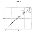
- Fig. 1 illustrates the relationship between the amplitude levels of an input signal and an output signal
- Fig. 2 is a circuit diagram of an exemplary Volterra filter
- Fig. 3 illustrates a memory effect canceller that includes a Volterra filter and a coefficient computing unit
- Fig. 4 is a block diagram of a schematic configuration of a radio frequency transmitter to which a memory effect canceller of an embodiment is applied.
- Fig. 5 illustrates an exemplary circuit configuration of the memory effect canceller of the embodiment.
- Digital pre-distortion has a problem in that a memory effect of a power amplifier is generated as the bandwidth of a transmission signal increases.
- the performance of digital pre-distortion in which the memory effect has not been taken into consideration, may considerably decrease with increasing bandwidth of an input signal.
- Fig. 1 illustrates the relationship between the amplitude level of an input signal Xin and the amplitude level of an output signal Yout (AM-AM characteristics), where (a) shows the AM-AM characteristics of a power amplifier having no memory effect and (b) shows the AM-AM characteristics of a power amplifier having a memory effect.
- AM-AM characteristics shows the AM-AM characteristics of a power amplifier having no memory effect
- a power amplifier having no memory effect also has nonlinear characteristics, in which the amplitude level of the output signal is distorted, in a region where the input signal amplitude level is high.
- a power amplifier having a memory effect has hysteresis characteristics in addition to nonlinear characteristics. That is, in a power amplifier having a memory effect, the amplitude level of the output signal Yout at a certain time depends not only on the input signal Xin at this time but also on the input signal Xin prior to this time.
- a method using a Volterra series is an example of a method of modeling the nonlinear input output characteristics of a power amplifier taking into consideration the hysteresis characteristics due to a memory effect.
- An input output characteristics model (Volterra model) using the Volterra series is represented by polynomial approximation as shown by the following Equation (1), for example. Note that in Equation (1), x(n) and y(n) are respectively a discrete-time input signal and a discrete-time output signal, and h 1 (q) and h 2 (q 1 , q 2 ) are coefficients as Volterra kernels.
- Equation (1) shows that, when Q is an index indicating the magnitude of a memory effect, as Q becomes larger an output signal at a given time depends on more samples of an input signal prior to the given time.
- Q and the hysteresis width illustrated by (b) in Fig. 1 have a relationship in which they are equivalent to each other.
- a circuit based on Equation (1) described above is a circuit illustrated in Fig. 2 .
- x[n] is a discrete-time input signal
- y[n] is a discrete-time output signal.
- the Volterra filter illustrated in Fig. 2 includes a delay element ( ⁇ ) 201 for the input signal x[n], multipliers 202 to 204, amplifiers 205 to 209 that perform amplification in accordance with the above-described coefficients (h 1[ 0], h 1 [l], h 2 [0, 0], h 2 [0, 1], and h 2 [l, 1] in Fig. 2 ), and adders 210 to 214.
- Equation (1) The low-order Volterra model shown by Equation (1) is only an example. It is known that when K is a value indicating the degree of the nonlinearity in a general Volterra model, the number of undefined coefficients yet to be computed increases with an order of (Q + 1) k .
- a memory effect canceller includes a Volterra filter 301 and a coefficient computing unit 302
- the coefficients of the Volterra model are computed in the coefficient computing unit 302 through feedback of the output signal y[n] of a power amplifier (HPA: high-power amplifier) 51.
- the Volterra filter 301 is a digital filter that performs signal processing on the input signal x[n], using the coefficients computed by the coefficient computing unit 302, in such a manner as to cancel out the memory effect of the power amplifier.
- the amount of computation exponentially increases with increasing Q.
- a memory effect canceller for cancelling out the memory effect of a power amplifier that amplifies an RF signal of a radio frequency transmitter to a desired level is described with reference to Fig. 4 .
- Fig. 4 is a block diagram of a schematic configuration of a radio frequency transmitter to which a memory effect canceller 100 of the embodiment is applied.
- this radio frequency transmitter includes a pre-distorter 2, a mixer 6, a signal conversion unit (TX) 50, a power amplifier (HPA: high-power amplifier) 51, an adder 52, a signal conversion unit (RX) 80, and the memory effect canceller 100.
- the pre-distorter 2 that compensates for the nonlinearity of the power amplifier 51 and the memory effect canceller 100 for compensating for the memory effect of the power amplifier 51 are separately provided.
- the signal conversion unit 80 demodulates an output signal (RF signal) of the radio frequency transmitter using orthogonal detection to convert it into a baseband signal, and converts an analog signal to a digital signal to generate a digital baseband signal. This baseband digital signal is fed back to the pre-distorter 2.
- the pre-distorter 2 computes distortion compensation coefficients representing the inverse characteristics of the nonlinearity (distortion) of the power amplifier 51 based on the input signal (digital baseband signal) and a signal (feedback signal) fed back from the signal conversion unit 80. At this time, the pre-distorter 2 compares the transmission signal prior to distortion compensation and the feedback signal from the signal conversion unit 80 based on adaptive signal processing using an LMS algorithm, computes the distortion compensation coefficients so as to make the error be zero, and successively updates the coefficients. The input signal is multiplied by the distortion compensation coefficients using the mixer 6, whereby the input signal is subjected to pre-distortion processing. Note that digital pre-distortion using an LMS algorithm has been disclosed in many patent literatures including Japanese Patent No. 4308163 , and the detailed description thereof is omitted here.
- the signal conversion unit 50 performs digital-to-analog conversion on the transmission signal (output signal of the mixer 6) having been subjected to the pre-distortion processing, and performs orthogonal modulation to generate an RF signal. This RF signal is supplied to the power amplifier 51.
- the transmission signal (output signal of the mixer 6) having been subjected to the pre-distortion processing is also input to the memory effect canceller 100 so as to suppress the memory effect of the power amplifier 51.
- the memory effect canceller 100 successively generates a correction signal for suppressing the memory effect of the power amplifier 51 and supplies it to the adder 52.
- the adder 52 adds the correction signal from the memory effect canceller 100 to the RF signal amplified by the power amplifier 51 to successively generate the RF output signal which has been compensated for the memory effect of the power amplifier 51.
- x[n] represents a digital baseband signal (transmission signal subsequent to the pre-distortion processing) obtained from the mixer 6 (refer to Fig. 4 ) as a discrete-time signal.
- An output signal y'[n] of the power amplifier 51 is a signal on which cancelling out of the memory effect of the power amplifier 51 has not been performed.
- a correction signal ⁇ y[n] obtained by the memory effect canceller 100 is added to y'[n], whereby the output signal y[n] of the power amplifier 51 in which the memory effect has been cancelled out is obtained.
- the output signal y'[n] of the power amplifier including the memory effect depends not only on the current input signal given as a transmission signal but also on the past input signal.
- the memory effect canceller 100 of the embodiment generates, as the correction signal Ay[n], a signal which is a weighted linear combination of the partial derivatives of the known transfer function F of the power amplifier, where given weight coefficients are used for the weighting, and the derivatives are obtained based on samples at respective times. That is, the correction signal Ay[n] is given by Equation (2) below.
- ⁇ ⁇ y n ⁇ 0 ⁇ dF x n , x ⁇ n - 1 , ... d x n + ⁇ 1 ⁇ dF x n , x ⁇ n - 1 , ... d x ⁇ n - 1 + ...
- the memory effect canceller 100 illustrated in Fig. 5 is configured to generate the correction signal ⁇ y[n] represented by Equation (2) above.
- the memory effect canceller 100 includes a delay unit 61 (first delay unit), delay units 62-1 to 62-Q (second delay unit), delay units 63-1 to 63-Q (first delay unit), a subtracter 65, computing units 70-0 to 70-Q, multipliers 72-0 to 72-Q, an adder 75, and a signal conversion unit 76.
- Fig. 5 also illustrates the signal conversion unit 50, the power amplifier 51, and the adder 52, in addition to the memory effect canceller 100.
- the adder 52 since the output signal y[n] in which the memory effect has been cancelled out is generated through the operation of the adder 52, the adder 52 may be considered to be part of the memory effect canceller 100.
- the delay unit 61, the delay units 62-1 to 62-Q, the delay units 63-1 to 63-Q, and the subtracter 65 make up a sample obtaining unit.
- the computing units 70-0 to 70-Q, the multipliers 72-0 to 72-Q, the adder 75, and the signal conversion unit 76 make up a signal generation unit.
- the adder 52 makes up a signal correction unit.
- the delay unit 61 generates sample x[n - 1] which is sample x[n] of the current transmission signal delayed by one sample period.
- the subtracter 65 subtracts sample x[n - 1] from sample x[n] to generate sample ⁇ x[n] of a difference signal.
- the delay unit 62-1 generates sample ⁇ x[n - 1] which is sample ⁇ x[n] delayed by one sample period.
- the delay units 62-2 to 62-Q generate samples ⁇ x[n - 2] to ⁇ x[n - Q] which are samples of the difference signal delayed by one sample period in sequence.
- the delay unit 63-1 generates sample x[n - 1] which is sample x[n] delayed by one sample period.
- the delay units 63-2 to 63-Q generate samples x[n - 2] to x[n - Q] which are samples of the transmission signal delayed by one sample period in sequence.
- the computing unit 70-0 computes a partial derivative of the known transfer function F of the power amplifier 51 using the samples at the current time, based on sample x[n] of the transmission signal and sample ⁇ x[n] of the difference signal.
- the computing units 70-1 to 70-Q compute partial derivatives of the known transfer function F of the power amplifier 51 using the samples at respective times, based on samples x[n - 1] to x[n - Q] of the transmission signal and samples ⁇ x[n - 1] to ⁇ x[n - Q] of the difference signal.
- the partial derivatives obtained by the computing units 70-0 to 70-Q correspond to the respective terms in Equation (2) without the weighting coefficients ⁇ 0 , ⁇ 1,
- the multipliers 72-0 to 72-Q multiply signals, indicating derivatives obtained by the computing units 70-0 to 70-Q, by the respective weighting coefficients ⁇ 0 to ⁇ Q .
- the adder 75 adds all the signals obtained by the multipliers 72-0 to 72-Q. Thereby, a baseband correction signal (digital signal) is obtained.
- the signal conversion unit 76 converts the digital signal obtained by the adder 75 into an analog signal and performs orthogonal conversion to convert the analog signal into a signal in a radio frequency band.
- the signal obtained by the signal conversion unit 76 is supplied to the adder 52 as the correction signal ⁇ y[n] of the memory effect canceller 100.
- y'[n] is a signal which has been obtained by converting a digital baseband signal (after having been subjected to pre-distortion processing) obtained by the mixer 6 (refer to Fig. 4 ) into an analog signal and then into a signal in a radio frequency band through the signal conversion unit 50, and further subjecting the signal to power amplification performed by the power amplifier 51. That is, as described above, y'[n] is a signal in which the memory effect of the power amplifier 51 has not been cancelled out. In the memory effect canceller 100 of the embodiment, the output signal y[n] in which the memory effect has been cancelled out is obtained by adding the correction signal Ay[n] to y'[n] thus obtained.
- weighting coefficients ⁇ 0 to ⁇ Q have been set in advance within a range of from 0 to 1, for example.
- a complex number coefficient in other words, a real number component and an imaginary number component, separately, may be set.
- computer results showed that the memory effect of the power amplifier 51 may be sufficiently suppressed. That is, it was determined that the width of the hysteresis in the input output characteristics of the power amplifier 51 due to a memory effect is considerably reduced.
- the inventor performed simulation of a two-tone test to measure the level of inter-modulation distortion (IMD). According to the results, it was determined that an allowance for a decrease in power level measured in the two-tone test was approximately 3 to 4 dB in the radio frequency transmitter provided with only DPD, but the allowance for a decrease in power level described above reached at least 10 dB in the radio frequency transmitter (with the configuration illustrated in Fig. 4 ) provided with the memory effect canceller 100 according to the embodiment in addition to DPD.
- IMD inter-modulation distortion
- an increase in the amount of computation when the order (that is, the number of samples: Q + 1) of the transfer function F used as a model of the power amplifier is proportional to Q. This is because, for computation of a correction signal, computation results based on the samples of a transmission signal and the samples of a difference signal are only linearly combined. Consequently, an exponential increase, such as that with (Q + 1) K , in computation amount with an increase in degree does not occur.
- a memory effect canceller for compensating for the nonlinear characteristics of a power amplifier may be provided separately from a pre-distorter for pre-distortion processing, as illustrated in Fig. 4 . That is, since the memory effect canceller is not built into the pre-distorter, processing for compensating for the nonlinear characteristics and processing for suppressing the memory effect are distributed, whereby the computation load of the whole radio frequency transmitter is lowered.
- an increase in the computation amount at the time of compensating for the memory effect of the power amplifier may be suppressed.
Landscapes
- Physics & Mathematics (AREA)
- Nonlinear Science (AREA)
- Engineering & Computer Science (AREA)
- Power Engineering (AREA)
- Amplifiers (AREA)
- Transmitters (AREA)
Abstract
Description
- Embodiments described herein relate to memory effect cancellers for power amplifiers that amplify transmission signals, transmitters using the memory effect cancellers, and memory effect cancelling method.
- To increase the efficiency of power amplifiers in radio frequency transmitters, the power amplifiers are frequently operated in a nonlinear region. However, such an operation method causes high-level inter-modulation distortion (IMD) to be generated, resulting in an increase in leakage power between neighboring channels. This is specifically noticeable in orthogonal frequency division multiplexing (OFDM) in which a peak-to-average power ratio (PAPR) is large. Further, since constellation (position in the complex plane of a signal) in modulation of a signal is distorted due to the nonlinearity of power amplifiers, an error vector magnitude (EVM) is deteriorated, resulting in an increase in bit error rate (BER).
- Digital pre-distortion (DPD) is suggested as a method for improving the nonlinear characteristics of power amplifiers. For example, in the case of adaptive pre-distortion, which is one of the pre-distortion methods, in consideration of the nonlinearity of a power amplifier an input signal is multiplied in advance by a compensation coefficient that represents the characteristics that are the inverse of those of the nonlinearity, thereby making the input signal prior to amplification be subjected to pre-distortion processing. When the compensated input signal is amplified by the power amplifier, the characteristics (inverse characteristics described above) given to the input signal are cancelled out by the nonlinearity of the power amplifier, allowing the power amplifier to have linear output characteristics. Digital pre-distortion is a reliable method for linearization of power amplifiers in terms of efficiency and cost.
- Accordingly, it is an object in one aspect of the embodiments discussed herein to provide a memory effect canceller and a radio frequency transmitter, enabling suppression of an increase in the computation amount at the time of compensating for the memory effect of a power amplifier.
- According to an aspect of the embodiments discussed herein, a memory effect canceller includes a sample obtaining section that obtains a plurality of discrete-time samples of a transmission signal supplied to a power amplifier that amplifies a transmission signal, a signal generation section that generates a correction signal that is a weighted linear combination, using given weighting coefficients, of partial derivatives of a transfer function of the power amplifier, wherein the transfer function has been defined in advance with a plurality of discrete-time samples as input variables, and wherein the partial derivatives are based on the discrete-time samples obtained by the sample obtaining section at respective times, and a signal correction section that corrects an output signal of the power amplifier based on the correction signal.
-
Fig. 1 illustrates the relationship between the amplitude levels of an input signal and an output signal; -
Fig. 2 is a circuit diagram of an exemplary Volterra filter; -
Fig. 3 illustrates a memory effect canceller that includes a Volterra filter and a coefficient computing unit; -
Fig. 4 is a block diagram of a schematic configuration of a radio frequency transmitter to which a memory effect canceller of an embodiment is applied; and -
Fig. 5 illustrates an exemplary circuit configuration of the memory effect canceller of the embodiment. - Regarding the embodiments discussed herein, the following observations are made.
- Digital pre-distortion has a problem in that a memory effect of a power amplifier is generated as the bandwidth of a transmission signal increases. The performance of digital pre-distortion in which the memory effect has not been taken into consideration, may considerably decrease with increasing bandwidth of an input signal.
- In general, the influence of the memory effect of a power amplifier is seen in the AM-AM characteristics and AM-PM characteristics which are the input output characteristics of the power amplifier. For example,
Fig. 1 illustrates the relationship between the amplitude level of an input signal Xin and the amplitude level of an output signal Yout (AM-AM characteristics), where (a) shows the AM-AM characteristics of a power amplifier having no memory effect and (b) shows the AM-AM characteristics of a power amplifier having a memory effect. As illustrated by (a) inFig. 1 , a power amplifier having no memory effect also has nonlinear characteristics, in which the amplitude level of the output signal is distorted, in a region where the input signal amplitude level is high. As illustrated by (b) inFig. 1 , a power amplifier having a memory effect has hysteresis characteristics in addition to nonlinear characteristics. That is, in a power amplifier having a memory effect, the amplitude level of the output signal Yout at a certain time depends not only on the input signal Xin at this time but also on the input signal Xin prior to this time. - A method using a Volterra series is an example of a method of modeling the nonlinear input output characteristics of a power amplifier taking into consideration the hysteresis characteristics due to a memory effect. An input output characteristics model (Volterra model) using the Volterra series is represented by polynomial approximation as shown by the following Equation (1), for example. Note that in Equation (1), x(n) and y(n) are respectively a discrete-time input signal and a discrete-time output signal, and h1(q) and h2(q1, q2) are coefficients as Volterra kernels. Equation (1) below shows that, when Q is an index indicating the magnitude of a memory effect, as Q becomes larger an output signal at a given time depends on more samples of an input signal prior to the given time. The case of Q = 0 corresponds to a memoryless power amplifier. Q and the hysteresis width illustrated by (b) in
Fig. 1 have a relationship in which they are equivalent to each other. -

- An example of a circuit based on Equation (1) described above is a circuit illustrated in
Fig. 2 . InFig. 2 , x[n] is a discrete-time input signal and y[n] is a discrete-time output signal. The Volterra filter illustrated inFig. 2 includes a delay element (τ) 201 for the input signal x[n], multipliers 202 to 204, amplifiers 205 to 209 that perform amplification in accordance with the above-described coefficients (h1[0], h1[l], h2[0, 0], h2[0, 1], and h2[l, 1] inFig. 2 ), andadders 210 to 214. - The low-order Volterra model shown by Equation (1) is only an example. It is known that when K is a value indicating the degree of the nonlinearity in a general Volterra model, the number of undefined coefficients yet to be computed increases with an order of (Q + 1)k.
- For example, referring to
Fig. 3 , supposing the case in which a memory effect canceller includes a Volterra filter 301 and a coefficient computing unit 302, the coefficients of the Volterra model are computed in the coefficient computing unit 302 through feedback of the output signal y[n] of a power amplifier (HPA: high-power amplifier) 51. The Volterra filter 301 is a digital filter that performs signal processing on the input signal x[n], using the coefficients computed by the coefficient computing unit 302, in such a manner as to cancel out the memory effect of the power amplifier. In the coefficient computing unit 302, the amount of computation exponentially increases with increasing Q. - The increase in the computation amount described above has a considerably larger influence in the case where the memory effect canceller illustrated in
Fig. 3 is built into DPD which uses a least mean square (LMS)-based algorithm. In other words, when polynomial approximation, such as a Volterra model, is built into DPD which uses an LMS-based algorithm, the amount of computation exponentially increases with increasing Q. This may cause a problem in that the algorithm does not converge, resulting in an unstable operation. On the other hand, when Q is set to a small value, coefficients in which the memory effect is sufficiently reflected cannot be set, and hence, the memory effect of the power amplifier is not sufficiently compensated for. - Hereinafter, an embodiment of a memory effect canceller for cancelling out the memory effect of a power amplifier that amplifies an RF signal of a radio frequency transmitter to a desired level is described with reference to
Fig. 4 . -
Fig. 4 is a block diagram of a schematic configuration of a radio frequency transmitter to which amemory effect canceller 100 of the embodiment is applied. - Referring to
Fig. 4 , this radio frequency transmitter includes a pre-distorter 2, a mixer 6, a signal conversion unit (TX) 50, a power amplifier (HPA: high-power amplifier) 51, anadder 52, a signal conversion unit (RX) 80, and thememory effect canceller 100. In this radio frequency transmitter, to lessen the operation load for compensating thepower amplifier 51, the pre-distorter 2 that compensates for the nonlinearity of thepower amplifier 51 and thememory effect canceller 100 for compensating for the memory effect of thepower amplifier 51 are separately provided. - Referring to
Fig. 4 , thesignal conversion unit 80 demodulates an output signal (RF signal) of the radio frequency transmitter using orthogonal detection to convert it into a baseband signal, and converts an analog signal to a digital signal to generate a digital baseband signal. This baseband digital signal is fed back to the pre-distorter 2. - The pre-distorter 2 computes distortion compensation coefficients representing the inverse characteristics of the nonlinearity (distortion) of the
power amplifier 51 based on the input signal (digital baseband signal) and a signal (feedback signal) fed back from thesignal conversion unit 80. At this time, the pre-distorter 2 compares the transmission signal prior to distortion compensation and the feedback signal from thesignal conversion unit 80 based on adaptive signal processing using an LMS algorithm, computes the distortion compensation coefficients so as to make the error be zero, and successively updates the coefficients. The input signal is multiplied by the distortion compensation coefficients using the mixer 6, whereby the input signal is subjected to pre-distortion processing. Note that digital pre-distortion using an LMS algorithm has been disclosed in many patent literatures including Japanese Patent No.4308163 - The
signal conversion unit 50 performs digital-to-analog conversion on the transmission signal (output signal of the mixer 6) having been subjected to the pre-distortion processing, and performs orthogonal modulation to generate an RF signal. This RF signal is supplied to thepower amplifier 51. - The transmission signal (output signal of the mixer 6) having been subjected to the pre-distortion processing is also input to the
memory effect canceller 100 so as to suppress the memory effect of thepower amplifier 51. Thememory effect canceller 100 successively generates a correction signal for suppressing the memory effect of thepower amplifier 51 and supplies it to theadder 52. Theadder 52 adds the correction signal from thememory effect canceller 100 to the RF signal amplified by thepower amplifier 51 to successively generate the RF output signal which has been compensated for the memory effect of thepower amplifier 51. - An exemplary configuration of the
memory effect canceller 100 will now be described with reference toFig. 5 . - Referring to
Fig. 5 , x[n] represents a digital baseband signal (transmission signal subsequent to the pre-distortion processing) obtained from the mixer 6 (refer toFig. 4 ) as a discrete-time signal. An output signal y'[n] of thepower amplifier 51 is a signal on which cancelling out of the memory effect of thepower amplifier 51 has not been performed. A correction signal Δy[n] obtained by thememory effect canceller 100 is added to y'[n], whereby the output signal y[n] of thepower amplifier 51 in which the memory effect has been cancelled out is obtained. - The output signal y'[n] of the power amplifier including the memory effect depends not only on the current input signal given as a transmission signal but also on the past input signal. Hence, the correction signal Ay[n] for the output signal is represented by Δy[n] = F{x[n], x[n - 1], ···, x[n - Q]}, where the current sample x[n] of the transmission signal and one or more past samples x[n], x[n - 1], ···, x[n - Q] are input parameters and F is an appropriate transfer function. For example, the transfer function F representing the power amplifier may be represented by a low-order Volterra model (in this case, the variables are only x[n] and x[n - 1]), where K = 3, Q = 1.
- Hence, the memory effect canceller 100 of the embodiment generates, as the correction signal Ay[n], a signal which is a weighted linear combination of the partial derivatives of the known transfer function F of the power amplifier, where given weight coefficients are used for the weighting, and the derivatives are obtained based on samples at respective times. That is, the correction signal Ay[n] is given by Equation (2) below.
-

- The
memory effect canceller 100 illustrated inFig. 5 is configured to generate the correction signal Δy[n] represented by Equation (2) above. - Referring again to
Fig. 5 , thememory effect canceller 100 includes a delay unit 61 (first delay unit), delay units 62-1 to 62-Q (second delay unit), delay units 63-1 to 63-Q (first delay unit), asubtracter 65, computing units 70-0 to 70-Q, multipliers 72-0 to 72-Q, anadder 75, and asignal conversion unit 76.Fig. 5 also illustrates thesignal conversion unit 50, thepower amplifier 51, and theadder 52, in addition to thememory effect canceller 100. In the embodiment, since the output signal y[n] in which the memory effect has been cancelled out is generated through the operation of theadder 52, theadder 52 may be considered to be part of thememory effect canceller 100. - The
delay unit 61, the delay units 62-1 to 62-Q, the delay units 63-1 to 63-Q, and thesubtracter 65 make up a sample obtaining unit. The computing units 70-0 to 70-Q, the multipliers 72-0 to 72-Q, theadder 75, and thesignal conversion unit 76 make up a signal generation unit. Theadder 52 makes up a signal correction unit. - Referring to
Fig. 5 , the operations of respective units of thememory effect canceller 100 will be described below. - The
delay unit 61 generates sample x[n - 1] which is sample x[n] of the current transmission signal delayed by one sample period. Thesubtracter 65 subtracts sample x[n - 1] from sample x[n] to generate sample Δx[n] of a difference signal. - The delay unit 62-1 generates sample Δx[n - 1] which is sample Δx[n] delayed by one sample period. Similarly, the delay units 62-2 to 62-Q generate samples Δx[n - 2] to Δx[n - Q] which are samples of the difference signal delayed by one sample period in sequence. The delay unit 63-1 generates sample x[n - 1] which is sample x[n] delayed by one sample period. Similarly, the delay units 63-2 to 63-Q generate samples x[n - 2] to x[n - Q] which are samples of the transmission signal delayed by one sample period in sequence.
- The computing unit 70-0 computes a partial derivative of the known transfer function F of the
power amplifier 51 using the samples at the current time, based on sample x[n] of the transmission signal and sample Δx[n] of the difference signal. Similarly, the computing units 70-1 to 70-Q compute partial derivatives of the known transfer function F of thepower amplifier 51 using the samples at respective times, based on samples x[n - 1] to x[n - Q] of the transmission signal and samples Δx[n - 1] to Δx[n - Q] of the difference signal. The partial derivatives obtained by the computing units 70-0 to 70-Q correspond to the respective terms in Equation (2) without the weighting coefficients α0, α1, - The multipliers 72-0 to 72-Q multiply signals, indicating derivatives obtained by the computing units 70-0 to 70-Q, by the respective weighting coefficients α0 to αQ. The
adder 75 adds all the signals obtained by the multipliers 72-0 to 72-Q. Thereby, a baseband correction signal (digital signal) is obtained. - The
signal conversion unit 76 converts the digital signal obtained by theadder 75 into an analog signal and performs orthogonal conversion to convert the analog signal into a signal in a radio frequency band. The signal obtained by thesignal conversion unit 76 is supplied to theadder 52 as the correction signal Δy[n] of thememory effect canceller 100. - Referring to
Fig. 5 , y'[n] is a signal which has been obtained by converting a digital baseband signal (after having been subjected to pre-distortion processing) obtained by the mixer 6 (refer toFig. 4 ) into an analog signal and then into a signal in a radio frequency band through thesignal conversion unit 50, and further subjecting the signal to power amplification performed by thepower amplifier 51. That is, as described above, y'[n] is a signal in which the memory effect of thepower amplifier 51 has not been cancelled out. In the memory effect canceller 100 of the embodiment, the output signal y[n] in which the memory effect has been cancelled out is obtained by adding the correction signal Ay[n] to y'[n] thus obtained. - Note that the weighting coefficients α0 to αQ have been set in advance within a range of from 0 to 1, for example. In correspondence with the orthogonal signal (I, Q) of the input signal, a complex number coefficient, in other words, a real number component and an imaginary number component, separately, may be set. A preferable example of weighting coefficient settings may be α0 = 0 and α1 = 1 for the case where a low-order Volterra model with K = 3 and Q = 1 is used as the transfer function F of the
power amplifier 51. With this example of weighting coefficient settings, computer results showed that the memory effect of thepower amplifier 51 may be sufficiently suppressed. That is, it was determined that the width of the hysteresis in the input output characteristics of thepower amplifier 51 due to a memory effect is considerably reduced. - In addition, the inventor performed simulation of a two-tone test to measure the level of inter-modulation distortion (IMD). According to the results, it was determined that an allowance for a decrease in power level measured in the two-tone test was approximately 3 to 4 dB in the radio frequency transmitter provided with only DPD, but the allowance for a decrease in power level described above reached at least 10 dB in the radio frequency transmitter (with the configuration illustrated in
Fig. 4 ) provided with thememory effect canceller 100 according to the embodiment in addition to DPD. - In the
memory effect canceller 100 according to the embodiment, an increase in the amount of computation when the order (that is, the number of samples: Q + 1) of the transfer function F used as a model of the power amplifier is proportional to Q. This is because, for computation of a correction signal, computation results based on the samples of a transmission signal and the samples of a difference signal are only linearly combined. Consequently, an exponential increase, such as that with (Q + 1)K, in computation amount with an increase in degree does not occur. - In the
memory effect canceller 100 according to the embodiment, a memory effect canceller for compensating for the nonlinear characteristics of a power amplifier may be provided separately from a pre-distorter for pre-distortion processing, as illustrated inFig. 4 . That is, since the memory effect canceller is not built into the pre-distorter, processing for compensating for the nonlinear characteristics and processing for suppressing the memory effect are distributed, whereby the computation load of the whole radio frequency transmitter is lowered. - According to the embodiments discussed herein, an increase in the computation amount at the time of compensating for the memory effect of the power amplifier may be suppressed.
- All examples and conditional language recited herein are intended for pedagogical purposes to aid the reader in understanding the invention and the concepts contributed by the inventor to furthering the art, and are to be construed as being without limitation to such specifically recited examples and conditions. Although the embodiments have been described in detail, it should be understood that the various changes, substitutions, and alterations could be made hereto without departing from the spirit and scope of the invention.
- In regard to the embodiments described above, the following additional descriptions are disclosed.
- (Additional Note 1)
A memory effect canceller including:- a sample obtaining section that obtains a plurality of discrete-time samples of a transmission signal supplied to a power amplifier that amplifies a transmission signal;
- a signal generation section that generates a correction signal that is a weighted linear combination, using given weighting coefficients, of partial derivatives of a transfer function of the power amplifier, wherein the transfer function has been defined in advance with a plurality of discrete-time samples as input variables, and wherein the partial derivatives are based on the discrete-time samples obtained by the sample obtaining section at respective times; and
- a signal correction section that corrects an output signal of the power amplifier based on the correction signal.
- (Additional Note 2)
The memory effect canceller according toAdditional Note 1, wherein the signal correction section includes an adder that adds the correction signal, after having been converted into a signal in a radio frequency band, to the output signal of the power amplifier. - (Additional Note 3)
The memory effect canceller according toAdditional Note - a plurality of first delay sections that delay a plurality of discrete-time samples in sequence;.
- a subtracter that computes difference values between neighboring samples among the plurality of discrete-time samples;
- a plurality of second delay sections that delay the difference values computed by the subtracter in sequence;
- a plurality of computing sections that compute derivatives of the transfer function using samples at respective times based on the outputs of the first and second delay sections;
- a plurality of multipliers that multiply derivatives, computed by the computing sections, respectively by the given weighting coefficients; and
- an adder that adds the multiplication results obtained by the plurality of the multipliers.
- (Additional Note 4)
A transmitter including:- a power amplifier that amplifies a transmission signal;
- a pre-distorter that performs pre-distortion processing on the transmission signal to compensate for nonlinear characteristics of the power amplifier based on a feedback signal fed back from the output side of the power amplifier, and outputs the transmission signal to the power amplifier; and
- a memory effect canceller that suppresses a memory effect of the power amplifier based on the transmission signal having been subjected to the pre-distortion processing performed by the pre-distorter,
- a sample obtaining section that obtains a plurality of discrete-time samples of a transmission signal supplied to the power amplifier;
- a signal generation section that generates a correction signal that is a weighted linear combination, using given weighting coefficients, of partial derivatives of a transfer function of the power amplifier, wherein the transfer function has been defined in advance with a plurality of discrete-time samples as input variables, and wherein the partial derivatives are based on the discrete-time samples obtained by the sample obtaining section at respective times; and
- a signal correction section that corrects an output signal of the power amplifier based on the correction signal.
- (Additional Note 5)
The transmitter according to Additional Note 4, wherein the signal correction section includes an adder that adds the correction signal, after having been converted into a signal in a radio frequency band, to the output signal of the power amplifier. - (Additional Note 6)
The transmitter according to Additional Note 4 or 5, wherein the signal generation section includes:- a plurality of first delay sections that delay a plurality of discrete-time samples in sequence;.
- a subtracter that computes difference values between neighboring samples among the plurality of discrete-time samples;
- a plurality of second delay sections that delay the difference values computed by the subtracter in sequence;
- a plurality of computing sections that compute derivatives of the transfer function using samples at respective times based on the outputs of the first and second delay sections;
- a plurality of multipliers that multiply derivatives, computed by the computing sections, respectively by the given weighting coefficients; and
- an adder that adds the multiplication results obtained by the plurality of the multipliers.
- (Additional Note 7)
A memory effect cancelling method including:- obtaining a plurality of discrete-time samples of a transmission signal supplied to a power amplifier that amplifies the transmission signal;
- generating a correction signal that is a weighted linear combination, using given weighting coefficients, of partial derivatives of a transfer function of the power amplifier, wherein the transfer function has been defined in advance with a plurality of discrete-time samples as input variables, and wherein the partial derivatives are based on the discrete-time samples at respective times; and
- correcting an output signal of the power amplifier based on the correction signal.
- (Additional Note 8)
The memory effect cancelling method according to Additional Note 7, wherein the correcting includes adding the correction signal, after having been converted into a signal in a radio frequency band, to the output signal of the power amplifier. - (Additional Note 9)
The memory effect cancelling method according to Additional Note 7 or 8, wherein the generating includes:- first delaying a plurality of discrete-time samples in sequence;.
- first computing difference values between neighboring samples among the plurality of discrete-time samples;
- second delaying the difference values computed in sequence;
- second computing derivatives of the transfer function using samples at respective times based on the outputs of the first and second delaying;
- multiplying derivatives, computed by the second computing, respectively by the given weighting coefficients; and
- adding the multiplication results obtained by the multiplying.


Claims (9)
- A memory effect canceller comprising:a sample obtaining section that obtains a plurality of discrete-time samples of a transmission signal supplied to a power amplifier that amplifies a transmission signal;a signal generation section that generates a correction signal that is a weighted linear combination, using given weighting coefficients, of partial derivatives of a transfer function of the power amplifier, wherein the transfer function has been defined in advance with a plurality of discrete-time samples as input variables, and wherein the partial derivatives are based on the discrete-time samples obtained by the sample obtaining section at respective times; anda signal correction section that corrects an output signal of the power amplifier based on the correction signal.
- The memory effect canceller according to Claim 1, wherein the signal correction section includes an adder that adds the correction signal, after having been converted into a signal in a radio frequency band, to the output signal of the power amplifier.
- The memory effect canceller according to Claim 1 or 2, wherein the signal generation section includes:a plurality of first delay sections that delay a plurality of discrete-time samples in sequence;.a subtracter that computes difference values between neighboring samples among the plurality of discrete-time samples;a plurality of second delay sections that delay the difference values computed by the subtracter in sequence;a plurality of computing sections that compute derivatives of the transfer function using samples at respective times based on the outputs of the first and second delay sections;a plurality of multipliers that multiply derivatives, computed by the computing sections, respectively by the given weighting coefficients; andan adder that adds the multiplication results obtained by the plurality of the multipliers.
- A transmitter comprising:a power amplifier that amplifies a transmission signal;a pre-distorter that performs pre-distortion processing on the transmission signal to compensate for nonlinear characteristics of the power amplifier based on a feedback signal fed back from the output side of the power amplifier, and outputs the transmission signal to the power amplifier; anda memory effect canceller that suppresses a memory effect of the power amplifier based on the transmission signal having been subjected to the pre-distortion processing performed by the pre-distorter,wherein the memory effect canceller includes:a sample obtaining section that obtains a plurality of discrete-time samples of a transmission signal supplied to the power amplifier;a signal generation section that generates a correction signal that is a weighted linear combination, using given weighting coefficients, of partial derivatives of a transfer function of the power amplifier, wherein the transfer function has been defined in advance with a plurality of discrete-time samples as input variables, and wherein the partial derivatives are based on the discrete-time samples obtained by the sample obtaining section at respective times; anda signal correction section that corrects an output signal of the power amplifier based on the correction signal.
- The transmitter according to Claim 4, wherein the signal correction section includes an adder that adds the correction signal, after having been converted into a signal in a radio frequency band, to the output signal of the power amplifier.
- The transmitter according to Claim 4 or 5, wherein the signal generation section includes:a plurality of first delay sections that delay a plurality of discrete-time samples in sequence;.a subtracter that computes difference values between neighboring samples among the plurality of discrete-time samples;a plurality of second delay sections that delay the difference values computed by the subtracter in sequence;a plurality of computing sections that compute derivatives of the transfer function using samples at respective times based on the outputs of the first and second delay sections;a plurality of multipliers that multiply derivatives, computed by the computing sections, respectively by the given weighting coefficients; andan adder that adds the multiplication results obtained by the plurality of the multipliers.
- A memory effect cancelling method comprising:obtaining a plurality of discrete-time samples of a transmission signal supplied to a power amplifier that amplifies the transmission signal;generating a correction signal that is a weighted linear combination, using given weighting coefficients, of partial derivatives of a transfer function of the power amplifier, wherein the transfer function has been defined in advance with a plurality of discrete-time samples as input variables, and wherein the partial derivatives are based on the discrete-time samples at respective times; andcorrecting an output signal of the power amplifier based on the correction signal.
- The memory effect cancelling method according to Claim 7, wherein the correcting includes adding the correction signal, after having been converted into a signal in a radio frequency band, to the output signal of the power amplifier.
- The memory effect cancelling method according to Claim 7 or 8, wherein the generating includes:first delaying a plurality of discrete-time samples in sequence;.first computing difference values between neighboring samples among the plurality of discrete-time samples;second delaying the difference values computed in sequence;second computing derivatives of the transfer function using samples at respective times based on the outputs of the first and second delaying;multiplying derivatives, computed by the second computing, respectively by the given weighting coefficients; andadding the multiplication results obtained by the multiplying.
Applications Claiming Priority (1)
| Application Number | Priority Date | Filing Date | Title |
|---|---|---|---|
| JP2010105759A JP5402817B2 (en) | 2010-04-30 | 2010-04-30 | Power amplifier memory effect canceller, wireless transmitter |
Publications (2)
| Publication Number | Publication Date |
|---|---|
| EP2383886A1 true EP2383886A1 (en) | 2011-11-02 |
| EP2383886B1 EP2383886B1 (en) | 2013-03-06 |
Family
ID=44117654
Family Applications (1)
| Application Number | Title | Priority Date | Filing Date |
|---|---|---|---|
| EP11164270A Not-in-force EP2383886B1 (en) | 2010-04-30 | 2011-04-29 | Memory effect canceller, transmitter, and memory effect cancelling method |
Country Status (3)
| Country | Link |
|---|---|
| US (1) | US8605819B2 (en) |
| EP (1) | EP2383886B1 (en) |
| JP (1) | JP5402817B2 (en) |
Cited By (1)
| Publication number | Priority date | Publication date | Assignee | Title |
|---|---|---|---|---|
| WO2015089090A1 (en) * | 2013-12-09 | 2015-06-18 | Qualcomm Incorporated | Quantitative characterization of nonlinearity and memory effect in nonlinear circuits |
Families Citing this family (25)
| Publication number | Priority date | Publication date | Assignee | Title |
|---|---|---|---|---|
| JP6037493B2 (en) * | 2011-10-13 | 2016-12-07 | 株式会社日立国際電気 | Distortion compensation circuit and transmitter using distortion compensation circuit and high-frequency power amplifier |
| US8804807B2 (en) * | 2012-06-13 | 2014-08-12 | Northrup Grumman Systems Corporation | Iterative equalization with non-linear soft interference cancellation in non-linear satellite channels |
| CN103701414B (en) * | 2012-09-28 | 2017-03-01 | 富士通株式会社 | The selecting device of nonlinear terms and method, identification system and compensation system |
| RU2660134C2 (en) * | 2012-12-18 | 2018-07-05 | Нуклеас Сайнтифик Инк. | Nonlinear system identification for optimisation of wireless power transfer |
| US8897728B2 (en) * | 2013-04-29 | 2014-11-25 | King Fahd University Of Petroleum And Minerals | Method for memory effects quantification and comparison in RF transmitters and amplifiers |
| US9893746B2 (en) * | 2015-06-25 | 2018-02-13 | Intel Corporation | Energy efficient polynomial kernel generation in full-duplex radio communication |
| US10033413B2 (en) * | 2016-05-19 | 2018-07-24 | Analog Devices Global | Mixed-mode digital predistortion |
| US10224970B2 (en) | 2016-05-19 | 2019-03-05 | Analog Devices Global | Wideband digital predistortion |
| EP3410605A1 (en) | 2017-06-02 | 2018-12-05 | Intel IP Corporation | Communication device and method for radio communication |
| US10985951B2 (en) | 2019-03-15 | 2021-04-20 | The Research Foundation for the State University | Integrating Volterra series model and deep neural networks to equalize nonlinear power amplifiers |
| US12206365B2 (en) | 2021-06-18 | 2025-01-21 | Qorvo Us, Inc. | Voltage ripple suppression in a transmission circuit |
| US12231088B2 (en) | 2021-06-18 | 2025-02-18 | Qorvo Us, Inc. | Wideband transmission circuit |
| US12057813B2 (en) | 2021-06-18 | 2024-08-06 | Qorvo Us, Inc. | Wideband transmission circuit |
| US11942899B2 (en) | 2021-06-18 | 2024-03-26 | Qorvo Us, Inc. | Envelope tracking voltage correction in a transmission circuit |
| US12199577B2 (en) | 2021-06-18 | 2025-01-14 | Qorvo Us, Inc. | Envelope tracking voltage correction in a transmission circuit |
| US11962338B2 (en) | 2021-09-16 | 2024-04-16 | Qorvo Us, Inc. | Equalization filter calibration in a transceiver circuit |
| US12284003B2 (en) | 2021-09-16 | 2025-04-22 | Qorvo Us, Inc. | Phase and amplitude error correction in a transmission circuit |
| US12401332B2 (en) | 2021-09-16 | 2025-08-26 | Qorvo Us, Inc. | Phase and amplitude error correction in a transmission circuit |
| US12323174B2 (en) | 2021-09-16 | 2025-06-03 | Qorvo Us, Inc. | Amplitude-to-phase error correction in a transceiver circuit |
| WO2023141443A1 (en) | 2022-01-18 | 2023-07-27 | Qorvo Us, Inc. | Linearized front-end operation using information from baseband circuit |
| US12273081B2 (en) | 2022-01-27 | 2025-04-08 | Qorvo Us, Inc. | Voltage ripple reduction in a power management circuit |
| US12549138B1 (en) | 2022-04-12 | 2026-02-10 | Qorvo Us, Inc. | Bandwidth adaptation in a transmission circuit |
| US12489402B2 (en) | 2022-05-31 | 2025-12-02 | Qorvo Us, Inc. | Voltage ripple reduction in a power management circuit |
| US12381525B2 (en) * | 2022-06-28 | 2025-08-05 | Qorvo Us, Inc. | Amplifier system |
| US12456957B2 (en) | 2023-01-20 | 2025-10-28 | Qorvo Us, Inc. | Amplitude and phase error correction in a wireless communication circuit |
Citations (2)
| Publication number | Priority date | Publication date | Assignee | Title |
|---|---|---|---|---|
| WO2005124995A1 (en) * | 2004-06-18 | 2005-12-29 | Filtronic Plc | Method and circuit for pre-distorting an input signal for supply to an amplifier |
| JP4308163B2 (en) | 2005-03-22 | 2009-08-05 | 富士通株式会社 | Distortion compensation device |
Family Cites Families (9)
| Publication number | Priority date | Publication date | Assignee | Title |
|---|---|---|---|---|
| JPH04308163A (en) | 1991-04-08 | 1992-10-30 | Aitetsukusu:Kk | Tail thread forming mechanism for thread winding device |
| US5760646A (en) * | 1996-03-29 | 1998-06-02 | Spectrian | Feed-forward correction loop with adaptive predistortion injection for linearization of RF power amplifier |
| US5898338A (en) * | 1996-09-20 | 1999-04-27 | Spectrian | Adaptive digital predistortion linearization and feed-forward correction of RF power amplifier |
| US5959500A (en) * | 1998-01-26 | 1999-09-28 | Glenayre Electronics, Inc. | Model-based adaptive feedforward amplifier linearizer |
| JP4356384B2 (en) | 2003-07-09 | 2009-11-04 | 日本電気株式会社 | Nonlinear compensation circuit, transmitter, and nonlinear compensation method |
| JP4394409B2 (en) * | 2003-09-25 | 2010-01-06 | 株式会社日立国際電気 | Predistortion type amplifier with distortion compensation function |
| JP4417174B2 (en) * | 2004-05-19 | 2010-02-17 | 株式会社日立国際電気 | Predistorter |
| DE602005006119T2 (en) * | 2005-07-21 | 2008-12-24 | Alcatel Lucent | Editing method for configuration data of a telecommunication system and computer product and server therefor |
| US7822146B2 (en) * | 2006-12-01 | 2010-10-26 | Texas Instruments Incorporated | System and method for digitally correcting a non-linear element |
-
2010
- 2010-04-30 JP JP2010105759A patent/JP5402817B2/en not_active Expired - Fee Related
-
2011
- 2011-04-26 US US13/094,319 patent/US8605819B2/en not_active Expired - Fee Related
- 2011-04-29 EP EP11164270A patent/EP2383886B1/en not_active Not-in-force
Patent Citations (2)
| Publication number | Priority date | Publication date | Assignee | Title |
|---|---|---|---|---|
| WO2005124995A1 (en) * | 2004-06-18 | 2005-12-29 | Filtronic Plc | Method and circuit for pre-distorting an input signal for supply to an amplifier |
| JP4308163B2 (en) | 2005-03-22 | 2009-08-05 | 富士通株式会社 | Distortion compensation device |
Cited By (1)
| Publication number | Priority date | Publication date | Assignee | Title |
|---|---|---|---|---|
| WO2015089090A1 (en) * | 2013-12-09 | 2015-06-18 | Qualcomm Incorporated | Quantitative characterization of nonlinearity and memory effect in nonlinear circuits |
Also Published As
| Publication number | Publication date |
|---|---|
| JP2011234322A (en) | 2011-11-17 |
| US8605819B2 (en) | 2013-12-10 |
| JP5402817B2 (en) | 2014-01-29 |
| EP2383886B1 (en) | 2013-03-06 |
| US20110268226A1 (en) | 2011-11-03 |
Similar Documents
| Publication | Publication Date | Title |
|---|---|---|
| EP2383886B1 (en) | Memory effect canceller, transmitter, and memory effect cancelling method | |
| US11129076B2 (en) | Method and system for baseband predistortion linearization in multi-channel wideband communication systems | |
| CN100426663C (en) | Digital predistorter using power series model | |
| US7944295B2 (en) | Predistorter | |
| EP2130296B1 (en) | Linearization of rf power amplifiers using an adaptive subband predistorter | |
| US6956433B2 (en) | Polynomial predistorter using complex vector multiplication | |
| CN100559720C (en) | Digital predistortion system and method for linearizing RF power amplifiers with nonlinear gain characteristics and memory effects | |
| CN101156159B (en) | Digital predistortion system and method for high efficiency transmitter | |
| JP5556643B2 (en) | Amplifying device and distortion compensation method | |
| CN100477500C (en) | Power amplifier predistorter and base station comprising same | |
| US20110163806A1 (en) | Distortion compensation amplification device | |
| US8933752B2 (en) | Power amplifier apparatus, distortion compensation coefficient updating method, and transmission apparatus | |
| KR20050108160A (en) | Digital predistortion apparatus and method in power amplifier | |
| US8564368B1 (en) | Digital Predistorter (DPD) structure based on dynamic deviation reduction (DDR)-based volterra series | |
| JP2008294518A (en) | Transmitter | |
| JP5387445B2 (en) | Predistortion compensation circuit and memory effect distortion compensation method for power amplifier | |
| KR100487209B1 (en) | Predistortion apparatus and method for compensating non-linearility of the power amplifier using look-up table | |
| KR100395263B1 (en) | Apparatus For Amplifier Linerarization |
Legal Events
| Date | Code | Title | Description |
|---|---|---|---|
| AK | Designated contracting states |
Kind code of ref document: A1 Designated state(s): AL AT BE BG CH CY CZ DE DK EE ES FI FR GB GR HR HU IE IS IT LI LT LU LV MC MK MT NL NO PL PT RO RS SE SI SK SM TR |
|
| AX | Request for extension of the european patent |
Extension state: BA ME |
|
| PUAI | Public reference made under article 153(3) epc to a published international application that has entered the european phase |
Free format text: ORIGINAL CODE: 0009012 |
|
| 17P | Request for examination filed |
Effective date: 20120502 |
|
| GRAP | Despatch of communication of intention to grant a patent |
Free format text: ORIGINAL CODE: EPIDOSNIGR1 |
|
| GRAS | Grant fee paid |
Free format text: ORIGINAL CODE: EPIDOSNIGR3 |
|
| GRAA | (expected) grant |
Free format text: ORIGINAL CODE: 0009210 |
|
| AK | Designated contracting states |
Kind code of ref document: B1 Designated state(s): AL AT BE BG CH CY CZ DE DK EE ES FI FR GB GR HR HU IE IS IT LI LT LU LV MC MK MT NL NO PL PT RO RS SE SI SK SM TR |
|
| REG | Reference to a national code |
Ref country code: GB Ref legal event code: FG4D |
|
| REG | Reference to a national code |
Ref country code: AT Ref legal event code: REF Ref document number: 600108 Country of ref document: AT Kind code of ref document: T Effective date: 20130315 Ref country code: CH Ref legal event code: EP |
|
| REG | Reference to a national code |
Ref country code: IE Ref legal event code: FG4D |
|
| REG | Reference to a national code |
Ref country code: DE Ref legal event code: R096 Ref document number: 602011000966 Country of ref document: DE Effective date: 20130502 |
|
| REG | Reference to a national code |
Ref country code: AT Ref legal event code: MK05 Ref document number: 600108 Country of ref document: AT Kind code of ref document: T Effective date: 20130306 |
|
| PG25 | Lapsed in a contracting state [announced via postgrant information from national office to epo] |
Ref country code: LT Free format text: LAPSE BECAUSE OF FAILURE TO SUBMIT A TRANSLATION OF THE DESCRIPTION OR TO PAY THE FEE WITHIN THE PRESCRIBED TIME-LIMIT Effective date: 20130306 Ref country code: SE Free format text: LAPSE BECAUSE OF FAILURE TO SUBMIT A TRANSLATION OF THE DESCRIPTION OR TO PAY THE FEE WITHIN THE PRESCRIBED TIME-LIMIT Effective date: 20130306 Ref country code: NO Free format text: LAPSE BECAUSE OF FAILURE TO SUBMIT A TRANSLATION OF THE DESCRIPTION OR TO PAY THE FEE WITHIN THE PRESCRIBED TIME-LIMIT Effective date: 20130606 Ref country code: BG Free format text: LAPSE BECAUSE OF FAILURE TO SUBMIT A TRANSLATION OF THE DESCRIPTION OR TO PAY THE FEE WITHIN THE PRESCRIBED TIME-LIMIT Effective date: 20130606 Ref country code: AT Free format text: LAPSE BECAUSE OF FAILURE TO SUBMIT A TRANSLATION OF THE DESCRIPTION OR TO PAY THE FEE WITHIN THE PRESCRIBED TIME-LIMIT Effective date: 20130306 Ref country code: ES Free format text: LAPSE BECAUSE OF FAILURE TO SUBMIT A TRANSLATION OF THE DESCRIPTION OR TO PAY THE FEE WITHIN THE PRESCRIBED TIME-LIMIT Effective date: 20130617 |
|
| REG | Reference to a national code |
Ref country code: NL Ref legal event code: VDEP Effective date: 20130306 |
|
| REG | Reference to a national code |
Ref country code: LT Ref legal event code: MG4D |
|
| PG25 | Lapsed in a contracting state [announced via postgrant information from national office to epo] |
Ref country code: LV Free format text: LAPSE BECAUSE OF FAILURE TO SUBMIT A TRANSLATION OF THE DESCRIPTION OR TO PAY THE FEE WITHIN THE PRESCRIBED TIME-LIMIT Effective date: 20130306 Ref country code: SI Free format text: LAPSE BECAUSE OF FAILURE TO SUBMIT A TRANSLATION OF THE DESCRIPTION OR TO PAY THE FEE WITHIN THE PRESCRIBED TIME-LIMIT Effective date: 20130306 Ref country code: FI Free format text: LAPSE BECAUSE OF FAILURE TO SUBMIT A TRANSLATION OF THE DESCRIPTION OR TO PAY THE FEE WITHIN THE PRESCRIBED TIME-LIMIT Effective date: 20130306 Ref country code: GR Free format text: LAPSE BECAUSE OF FAILURE TO SUBMIT A TRANSLATION OF THE DESCRIPTION OR TO PAY THE FEE WITHIN THE PRESCRIBED TIME-LIMIT Effective date: 20130607 |
|
| PG25 | Lapsed in a contracting state [announced via postgrant information from national office to epo] |
Ref country code: BE Free format text: LAPSE BECAUSE OF FAILURE TO SUBMIT A TRANSLATION OF THE DESCRIPTION OR TO PAY THE FEE WITHIN THE PRESCRIBED TIME-LIMIT Effective date: 20130306 Ref country code: HR Free format text: LAPSE BECAUSE OF FAILURE TO SUBMIT A TRANSLATION OF THE DESCRIPTION OR TO PAY THE FEE WITHIN THE PRESCRIBED TIME-LIMIT Effective date: 20130306 Ref country code: RS Free format text: LAPSE BECAUSE OF FAILURE TO SUBMIT A TRANSLATION OF THE DESCRIPTION OR TO PAY THE FEE WITHIN THE PRESCRIBED TIME-LIMIT Effective date: 20130306 |
|
| PG25 | Lapsed in a contracting state [announced via postgrant information from national office to epo] |
Ref country code: CZ Free format text: LAPSE BECAUSE OF FAILURE TO SUBMIT A TRANSLATION OF THE DESCRIPTION OR TO PAY THE FEE WITHIN THE PRESCRIBED TIME-LIMIT Effective date: 20130306 Ref country code: PT Free format text: LAPSE BECAUSE OF FAILURE TO SUBMIT A TRANSLATION OF THE DESCRIPTION OR TO PAY THE FEE WITHIN THE PRESCRIBED TIME-LIMIT Effective date: 20130708 Ref country code: RO Free format text: LAPSE BECAUSE OF FAILURE TO SUBMIT A TRANSLATION OF THE DESCRIPTION OR TO PAY THE FEE WITHIN THE PRESCRIBED TIME-LIMIT Effective date: 20130306 Ref country code: SK Free format text: LAPSE BECAUSE OF FAILURE TO SUBMIT A TRANSLATION OF THE DESCRIPTION OR TO PAY THE FEE WITHIN THE PRESCRIBED TIME-LIMIT Effective date: 20130306 Ref country code: EE Free format text: LAPSE BECAUSE OF FAILURE TO SUBMIT A TRANSLATION OF THE DESCRIPTION OR TO PAY THE FEE WITHIN THE PRESCRIBED TIME-LIMIT Effective date: 20130306 Ref country code: NL Free format text: LAPSE BECAUSE OF FAILURE TO SUBMIT A TRANSLATION OF THE DESCRIPTION OR TO PAY THE FEE WITHIN THE PRESCRIBED TIME-LIMIT Effective date: 20130306 Ref country code: IS Free format text: LAPSE BECAUSE OF FAILURE TO SUBMIT A TRANSLATION OF THE DESCRIPTION OR TO PAY THE FEE WITHIN THE PRESCRIBED TIME-LIMIT Effective date: 20130706 |
|
| PG25 | Lapsed in a contracting state [announced via postgrant information from national office to epo] |
Ref country code: PL Free format text: LAPSE BECAUSE OF FAILURE TO SUBMIT A TRANSLATION OF THE DESCRIPTION OR TO PAY THE FEE WITHIN THE PRESCRIBED TIME-LIMIT Effective date: 20130306 |
|
| PG25 | Lapsed in a contracting state [announced via postgrant information from national office to epo] |
Ref country code: MC Free format text: LAPSE BECAUSE OF FAILURE TO SUBMIT A TRANSLATION OF THE DESCRIPTION OR TO PAY THE FEE WITHIN THE PRESCRIBED TIME-LIMIT Effective date: 20130306 |
|
| PLBE | No opposition filed within time limit |
Free format text: ORIGINAL CODE: 0009261 |
|
| STAA | Information on the status of an ep patent application or granted ep patent |
Free format text: STATUS: NO OPPOSITION FILED WITHIN TIME LIMIT |
|
| REG | Reference to a national code |
Ref country code: IE Ref legal event code: MM4A |
|
| PG25 | Lapsed in a contracting state [announced via postgrant information from national office to epo] |
Ref country code: DK Free format text: LAPSE BECAUSE OF FAILURE TO SUBMIT A TRANSLATION OF THE DESCRIPTION OR TO PAY THE FEE WITHIN THE PRESCRIBED TIME-LIMIT Effective date: 20130306 |
|
| 26N | No opposition filed |
Effective date: 20131209 |
|
| PG25 | Lapsed in a contracting state [announced via postgrant information from national office to epo] |
Ref country code: IT Free format text: LAPSE BECAUSE OF FAILURE TO SUBMIT A TRANSLATION OF THE DESCRIPTION OR TO PAY THE FEE WITHIN THE PRESCRIBED TIME-LIMIT Effective date: 20130306 |
|
| REG | Reference to a national code |
Ref country code: DE Ref legal event code: R097 Ref document number: 602011000966 Country of ref document: DE Effective date: 20131209 |
|
| PG25 | Lapsed in a contracting state [announced via postgrant information from national office to epo] |
Ref country code: IE Free format text: LAPSE BECAUSE OF NON-PAYMENT OF DUE FEES Effective date: 20130429 |
|
| REG | Reference to a national code |
Ref country code: CH Ref legal event code: PL |
|
| PG25 | Lapsed in a contracting state [announced via postgrant information from national office to epo] |
Ref country code: CH Free format text: LAPSE BECAUSE OF NON-PAYMENT OF DUE FEES Effective date: 20140430 Ref country code: LI Free format text: LAPSE BECAUSE OF NON-PAYMENT OF DUE FEES Effective date: 20140430 |
|
| PG25 | Lapsed in a contracting state [announced via postgrant information from national office to epo] |
Ref country code: MT Free format text: LAPSE BECAUSE OF FAILURE TO SUBMIT A TRANSLATION OF THE DESCRIPTION OR TO PAY THE FEE WITHIN THE PRESCRIBED TIME-LIMIT Effective date: 20130306 |
|
| PG25 | Lapsed in a contracting state [announced via postgrant information from national office to epo] |
Ref country code: SM Free format text: LAPSE BECAUSE OF FAILURE TO SUBMIT A TRANSLATION OF THE DESCRIPTION OR TO PAY THE FEE WITHIN THE PRESCRIBED TIME-LIMIT Effective date: 20130306 |
|
| PG25 | Lapsed in a contracting state [announced via postgrant information from national office to epo] |
Ref country code: TR Free format text: LAPSE BECAUSE OF FAILURE TO SUBMIT A TRANSLATION OF THE DESCRIPTION OR TO PAY THE FEE WITHIN THE PRESCRIBED TIME-LIMIT Effective date: 20130306 Ref country code: CY Free format text: LAPSE BECAUSE OF FAILURE TO SUBMIT A TRANSLATION OF THE DESCRIPTION OR TO PAY THE FEE WITHIN THE PRESCRIBED TIME-LIMIT Effective date: 20130306 |
|
| PG25 | Lapsed in a contracting state [announced via postgrant information from national office to epo] |
Ref country code: MK Free format text: LAPSE BECAUSE OF FAILURE TO SUBMIT A TRANSLATION OF THE DESCRIPTION OR TO PAY THE FEE WITHIN THE PRESCRIBED TIME-LIMIT Effective date: 20130306 Ref country code: HU Free format text: LAPSE BECAUSE OF FAILURE TO SUBMIT A TRANSLATION OF THE DESCRIPTION OR TO PAY THE FEE WITHIN THE PRESCRIBED TIME-LIMIT; INVALID AB INITIO Effective date: 20110429 Ref country code: LU Free format text: LAPSE BECAUSE OF NON-PAYMENT OF DUE FEES Effective date: 20130429 |
|
| REG | Reference to a national code |
Ref country code: FR Ref legal event code: PLFP Year of fee payment: 6 |
|
| REG | Reference to a national code |
Ref country code: FR Ref legal event code: PLFP Year of fee payment: 7 |
|
| PGFP | Annual fee paid to national office [announced via postgrant information from national office to epo] |
Ref country code: FR Payment date: 20170313 Year of fee payment: 7 |
|
| PGFP | Annual fee paid to national office [announced via postgrant information from national office to epo] |
Ref country code: GB Payment date: 20170426 Year of fee payment: 7 Ref country code: DE Payment date: 20170426 Year of fee payment: 7 |
|
| PG25 | Lapsed in a contracting state [announced via postgrant information from national office to epo] |
Ref country code: AL Free format text: LAPSE BECAUSE OF FAILURE TO SUBMIT A TRANSLATION OF THE DESCRIPTION OR TO PAY THE FEE WITHIN THE PRESCRIBED TIME-LIMIT Effective date: 20130306 |
|
| REG | Reference to a national code |
Ref country code: DE Ref legal event code: R119 Ref document number: 602011000966 Country of ref document: DE |
|
| GBPC | Gb: european patent ceased through non-payment of renewal fee |
Effective date: 20180429 |
|
| PG25 | Lapsed in a contracting state [announced via postgrant information from national office to epo] |
Ref country code: DE Free format text: LAPSE BECAUSE OF NON-PAYMENT OF DUE FEES Effective date: 20181101 |
|
| PG25 | Lapsed in a contracting state [announced via postgrant information from national office to epo] |
Ref country code: GB Free format text: LAPSE BECAUSE OF NON-PAYMENT OF DUE FEES Effective date: 20180429 |
|
| PG25 | Lapsed in a contracting state [announced via postgrant information from national office to epo] |
Ref country code: FR Free format text: LAPSE BECAUSE OF NON-PAYMENT OF DUE FEES Effective date: 20180430 |