EP2383581A1 - Apparatus for monitoring fault current in power system - Google Patents
Apparatus for monitoring fault current in power system Download PDFInfo
- Publication number
- EP2383581A1 EP2383581A1 EP11163063A EP11163063A EP2383581A1 EP 2383581 A1 EP2383581 A1 EP 2383581A1 EP 11163063 A EP11163063 A EP 11163063A EP 11163063 A EP11163063 A EP 11163063A EP 2383581 A1 EP2383581 A1 EP 2383581A1
- Authority
- EP
- European Patent Office
- Prior art keywords
- signal
- output
- latch
- unit
- current
- Prior art date
- Legal status (The legal status is an assumption and is not a legal conclusion. Google has not performed a legal analysis and makes no representation as to the accuracy of the status listed.)
- Withdrawn
Links
- 238000012544 monitoring process Methods 0.000 title claims abstract description 11
- 230000004913 activation Effects 0.000 claims description 14
- 238000006243 chemical reaction Methods 0.000 claims description 3
- 230000004044 response Effects 0.000 abstract description 6
- 230000000630 rising effect Effects 0.000 abstract description 5
- 239000003990 capacitor Substances 0.000 abstract description 4
- 244000145845 chattering Species 0.000 abstract description 2
- 230000007257 malfunction Effects 0.000 abstract description 2
- 238000010586 diagram Methods 0.000 description 3
- 239000013256 coordination polymer Substances 0.000 description 2
- 230000009471 action Effects 0.000 description 1
- 238000012806 monitoring device Methods 0.000 description 1
Images


Classifications
-
- G—PHYSICS
- G01—MEASURING; TESTING
- G01R—MEASURING ELECTRIC VARIABLES; MEASURING MAGNETIC VARIABLES
- G01R19/00—Arrangements for measuring currents or voltages or for indicating presence or sign thereof
- G01R19/165—Indicating that current or voltage is either above or below a predetermined value or within or outside a predetermined range of values
- G01R19/16533—Indicating that current or voltage is either above or below a predetermined value or within or outside a predetermined range of values characterised by the application
- G01R19/16538—Indicating that current or voltage is either above or below a predetermined value or within or outside a predetermined range of values characterised by the application in AC or DC supplies
- G01R19/16547—Indicating that current or voltage is either above or below a predetermined value or within or outside a predetermined range of values characterised by the application in AC or DC supplies voltage or current in AC supplies
-
- G—PHYSICS
- G01—MEASURING; TESTING
- G01R—MEASURING ELECTRIC VARIABLES; MEASURING MAGNETIC VARIABLES
- G01R19/00—Arrangements for measuring currents or voltages or for indicating presence or sign thereof
- G01R19/10—Measuring sum, difference or ratio
-
- G—PHYSICS
- G01—MEASURING; TESTING
- G01R—MEASURING ELECTRIC VARIABLES; MEASURING MAGNETIC VARIABLES
- G01R19/00—Arrangements for measuring currents or voltages or for indicating presence or sign thereof
- G01R19/165—Indicating that current or voltage is either above or below a predetermined value or within or outside a predetermined range of values
- G01R19/16566—Circuits and arrangements for comparing voltage or current with one or several thresholds and for indicating the result not covered by subgroups G01R19/16504, G01R19/16528, G01R19/16533
- G01R19/16571—Circuits and arrangements for comparing voltage or current with one or several thresholds and for indicating the result not covered by subgroups G01R19/16504, G01R19/16528, G01R19/16533 comparing AC or DC current with one threshold, e.g. load current, over-current, surge current or fault current
Definitions
- An aspect of the present invention relates to an apparatus for monitoring a fault current in a power system, and more specifically, to an apparatus for quickly monitoring a fault current when an accident caused by a stroke of lightning or a short circuit occurs in a power system.
- Embodiments of the present invention provide an apparatus for monitoring a fault current in a power system, which does not rectify an AC signal detected from a power system to a DC signal but immediately monitors a fault current generated in the AC signal, thereby quickly responding to the power system.
- an apparatus for monitoring a fault current in a power system comprising: a first bridge diode configured to receive an AC current detected from a distribution line in the power system and full wave-rectify the received AC current; a second bridge diode configured to receive an AC voltage detected from the distribution line in the power system and full wave-rectify the received AC voltage; a first comparison unit configured to convert a current signal outputted from the first bridge diode into a voltage signal and output a high or low digital signal by comparing the converted voltage signal with a predetermined reference value; a second comparison unit configured to output a high or low digital signal by comparing a voltage signal outputted from the second bridge diode with a predetermined reference value; a first latch configured to latch an output value of the first comparison unit; a second latch unit configured to latch an output value of the second comparison unit; and a fault current output unit configured to output a fault signal informing that a fault current is generated based on the output values of the first and second latch
- the first comparison unit may include a buffer configured to convert the current signal outputted from the first bridge diode into a voltage signal through a resistive element for voltage conversion and output the converted voltage signal; a comparator configured to receive the output signal of the buffer and the reference value respectively through inverting and non-inverting input terminals of an operational amplifier and output a high or low digital signal by comparing the output signal with the reference value; and an inverter configured to invert the output signal of the comparator and output the inverted signal.
- the first latch unit may include a D latch having a digital signal input terminal to which a high signal is applied, a clock input terminal to which the output signal of the inverter is inputted, and an activation terminal connected to a switch unit that determines whether a latch operation is activated.
- the second comparison unit may include a buffer configured to recede a voltage signal outputted from the second bridge diode and output the received voltage signal; a comparator configured to receive the output signal of the buffer and the reference value respectively through inverting and non-inverting input terminals of an operational amplifier and output a high or low digital signal by comparing the output signal with the reference value; and an inverter configured to invert the output signal of the comparator and output the inverted signal.
- the second latch unit may include a D latch having a digital signal input terminal to which a high signal is applied, a clock input terminal to which the output signal of the inverter is inputted, and an activation terminal connected to a switch unit that determines whether a latch operation is activated.
- the reference value may be configured to be variably determined by a user using a variable resistive element.
- the apparatus may further include display units respectively connected to the first and second latch units so as to turn on/off light emitting diodes (LEDs) based on the output values thereof.
- LEDs light emitting diodes
- the apparatus may further include a display unit connected to the fault signal output unit so as to turn on/off an LED based on the output value thereof.
- FIG. 1 is a diagram schematically showing a configuration of an apparatus for monitoring a fault current in a power system according to an embodiment of the present invention
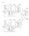
- FIG. 2 is a circuit diagram showing internal circuit configurations of a first comparison unit and a second comparison unit.
- FIG. 3 is a circuit diagram showing an embodiment of a configuration of a first latch unit, a second latch unit and a fault signal output unit related to the first and second comparison units shown in FIG. 2 .
- an apparatus 20 for monitoring a fault current in a power system receives an AC current from a current transformer 13 for detecting current from a distribution line 11 in the power system, and receives a voltage detected from a Rogowski coil 15.
- the fault current monitoring apparatus 20 includes a first bridge diode 21-1, a second bridge diode 21-2, a first comparison unit 23-1, a second comparison unit 23-2, a first latch unit 25-1, a second latch unit 25-2 and a fault signal output unit 27.
- the first bridge diode 21-1 receives an AC current from the current transformer 13 and full wave-rectifies the received AC current. Then, the first bridge diode 21-1 outputs the full-wave rectified AC current.
- the second bridge diode 21-2 receives the AC voltage from the Rogowski coil 15 and full wave-rectifies the received AC voltage. Then, the second bridge diode 21-2 outputs the full-wave rectified AC voltage.
- the Rogowski coil 15 detects current in the distribution line 11.
- the Rogowski 15 is connected to a resistive element so as to transfer an AC voltage to the fault current monitoring apparatus 20.
- the first and second bridge diodes 21-1 and 21-2 are used to full wave-rectify an AC current. However, the first and second bridge diodes 21-1 and 21-2 are not used to smooth the AC current to a DC current through a capacitor but used to monitor whether a fault signal is generated commonly with respect to both positive (+) and negative (-) regions of the AC signal.
- the first comparison unit 23-1 converts a current signal outputted from the first bridge diode 21-1 into a voltage signal, and outputs a high or low digital signal by comparing the converted voltage signal with a predetermined reference value.
- the first comparison unit 23-1 functions to determine whether a fault current is generated based on the AC current outputted from the first bridge diode 21-1 If necessary, the first comparison unit 23-1 may be variously configured.
- the second comparison unit 23-2 outputs a high or low digital signal by comparing the voltage signal outputted from the second bridge diode 21-2 with a predetermined reference value.
- the second comparison unit 23-2 functions to determine whether a fault current is generated based on the AC voltage outputted on the second bridge diode 21-2. If necessary, the second comparison unit 23-2 may be variously configured.
- the first comparison unit 23-1 may include a buffer 23-11, a comparator 23-12 and an inverter 23-13.
- the buffer 23-11 includes resistive elements R1 to R4 for voltage conversion, which converts a current signal outputted from the first bridge diode 21-1 into a voltage signal, and outputs an input voltage through an operational amplifier OP1 as it is.
- the comparator 23-12 may be configured using an operational amplifier OP2.
- An output signal from the buffer 23-11 is applied to an inverting input terminal of the operational amplifier OP2, and a reference value is inputted to a non-inverting input terminal of the operation amplifier OP2.
- the operational amplifier OP2 outputs a high digital signal. If the voltage applied to the inverting input terminal is greater than that inputted to the non-inverting input terminal, the operational amplifier OP2 outputs a low digital signal.
- the inverter 23-13 inverts an output signal from the comparator 23-12 and outputs the inverted signal.
- the comparator 23-12 outputs a low digital signal, and the digital signal is inverted by the inverter 23-13.
- the first comparison unit 23-1 outputs a high digital signal.
- the second comparison unit 23-2 may include a buffer 23-21, a comparator 23-22 and an inverter 23-23.
- the buffer 23-21 outputs an input voltage through an operational amplifier OP3 as it is.
- the comparator 23-22 may be configured using an operational amplifier OP4. An output signal from the buffer 23-21 is applied to an inverting input terminal of the operational amplifier OP4, and a reference value is inputted to a non-inverting input terminal of the operation amplifier OP4.
- the operational amplifier OP4 outputs a high digital signal. If the voltage applied to the inverting input terminal is greater than that inputted to the non-inverting input terminal, the operational amplifier OP4 outputs a low digital signal.
- the inverter 23-23 inverts an output signal from the comparator 23-22 and outputs the inverted signal.
- the comparator 23-22 outputs a low digital signal, and the digital signal is inverted by the inverter 23-23.
- the second comparison unit 23-2 outputs a high digital signal.
- the reference values of the first and second comparison units 23-1 and 23-2 may be configured to be variably determined by a user using variable resistive elements VR1 and VR2, respectively.
- the user can adjust the reference values by controlling the respective variable resistive elements VR1 and VR2.
- the reference value applied to the non-inverting input terminal of the operational amplifier OP2 in the comparator 23-12 of the first comparison unit 23-1 is determined by the following expression 1. resistance of VR ⁇ 1 resistance of R ⁇ 7 + resistance of VR ⁇ 1
- the reference value applied to the non-inverting input terminal of the operational amplifier OP4 in the comparator 23-22 of the second comparison unit 23-2 is determined by the following expression 2. resistance of VR ⁇ 2 resistance of R ⁇ 8 + resistance of VR ⁇ 2
- the first latch unit 25-1 latches an output value from the first comparison unit 23-1
- the second latch unit 25-2 latches an output value from the second comparison unit 23-2.
- the first and second latch units 25-1 and 25-2 function to store a signal informing that a fault is generated until they are reset.
- the fault signal output unit 27 outputs a fault signal informing that a fault current is generated according to the output values from the first and second latch units 25-1 and 25-2.
- first and second latch units 25-1 and 25-2 respectively connected to the first and second comparison units 23-1 and 23-2 shown in FIG. 2 will be described with reference to FIG. 3 .
- the first and second comparison units 23-1 and 23-2 respectively output high digital signals when a fault current is generated
- the first and second latch units 25-1 and 25-2 may be configured using D latches 35-1 and 35-2.
- a high signal is applied to a digital signal input terminal D of the D latch 35-1 in the first latch unit 25-1, and an output signal from the inverter 23-13 is inputted to a clock input terminal CP.
- An activation terminal IRD is connected to a switch unit 31-1 for determining the presence of activation of a latch operation.
- the switch unit 31-1 allows the user to determine the presence of the activation of the latch operation. If a low signal is inputted to the activation terminal IRD of the D latch 35-1, the latch operation is not activated. If a high signal is inputted to the activation terminal IRD of the D latch 35-1, the latch operation is activated.
- a high signal is applied to a digital signal input terminal D of the D latch 35-2 in the second latch unit 25-2, and an output signal from the inverter 23-23 is inputted to a clock input terminal CP.
- An activation terminal IRD is connected to a switch unit 31-2 for determining the presence of activation of a latch operation.
- the switch unit 31-2 allows the user to determine the presence of the activation of the latch operation. If a low signal is inputted to the activation terminal IRD of the D latch 35-2, the latch operation is not activated. If a high signal is inputted to the activation terminal IRD of the D latch 35-2, the latch operation is activated.
- the first and second latch units 25-1 and 25-2 respectively output high signals when a fault is generated, and hence the fault signal output unit 27 may be configured as an AND gate element.
- an AND gate element 27 outputs a fault signal when a fault is monitored from the AC current inputted from the current transformer 13 and the AC voltage inputted through the Rogowski coil 15.
- a display unit 33-1 for turning on/off a light emitting diode (LED) according to the output value of the first latch unit 25-1 may be connected to the first latch unit 25-1 so that the user can visually identify the presence of occurrence of an accident.
- LED light emitting diode
- the display unit 33-1 may be configured in a structure in which a resistive element 37-1 for current limiting, an LED 37-2 and an inverter 37-3 are connected in series to one another.
- a display unit 33-2 for turning on/off an LED according to the output value of the second latch unit 25-2 may be connected to the second latch unit 25-2 so that the user can visually identify the presence of occurrence of an accident.
- the display unit 33-2 may be configured in a structure in which a resistive element 38-1 for current limiting, an LED 38-2 and an inverter 38-3 are connected in series to one another.
- a display unit 33-3 for turning on/off an LED according to the output value of the fault signal output unit 27 may be connected to the fault signal output unit 27 so that the user can visually identify the presence of occurrence of an accident.
- the display unit 33-3 may be configured in a structure in which a resistive element 39-1 for current limiting, an LED 39-2 and an inverter 39-3 are connected in series to one another,
- an output terminal of the inverter 39-3 becomes a low state. Then, current flows from a power source to the LED 39-2 through the resistive element 39-1 for current limiting, and accordingly, the LED 39-2 is turned on.
- an AC signal detected from a power system is passed through a bridge diode, and in this state, the presence of occurrence of an accident is immediately determined.
- a response delay due to a rising time generated when the AC signal is smoothed to a DC signal through a capacitor it is possible to prevent a response delay due to a rising time generated when the AC signal is smoothed to a DC signal through a capacitor and to quickly respond to the power system.
- the presence of occurrence of a fault in the power system is parallely monitored using a current transformer and a Rogowski coil. If a fault waveform is generated once, it is latched so that a corresponding state is maintained until a reset is performed. Then, a fault signal is outputted when the fault is monitored from the current transformer and the Rogowski coil.
Landscapes
- Engineering & Computer Science (AREA)
- Power Engineering (AREA)
- Physics & Mathematics (AREA)
- General Physics & Mathematics (AREA)
- Emergency Protection Circuit Devices (AREA)
- Testing Of Short-Circuits, Discontinuities, Leakage, Or Incorrect Line Connections (AREA)
- Measurement Of Current Or Voltage (AREA)
Abstract
Disclosed is an apparatus (20) for monitoring a fault current in a power system. The apparatus does not rectify an AC signal detected from a power system but full wave-rectifies the AC signal using a bridge diode (21-1,21-2) and then monitors a fault current. Particularly, current and voltage in the power system are respectively detected through a current transformer (13) and a Rogowski coil (15), and presence of occurrence of an accident is parallely monitored using the detected current and voltage. Thus, it is possible to prevent a response delay due to a rising time generated when the AC signal is smoothed to a DC signal through a capacitor and to prevent malfunction caused by chattering while performing a fast response at the time when a fault current is generated for the first time.
Description
- An aspect of the present invention relates to an apparatus for monitoring a fault current in a power system, and more specifically, to an apparatus for quickly monitoring a fault current when an accident caused by a stroke of lightning or a short circuit occurs in a power system.
- When an accident caused by a stroke of lightning or a short circuit occurs in a power system, various apparatuses such as a superconducting fault current limiter or a digital protection relay are used to take action against the accident.
- In order to protect devices in a power system, conditions of occurrence of an accident should be monitored as quickly as possible. To this end, presence of fault current may be detected by rectifying an AC (Alternating Current) signal inputted from the power system to a DC (Direct Current) signal. In this case, a charging time (rising time) of a capacitor is necessarily required, and therefore, it is difficult to quickly determine the presence of occurrence of the accident.
- Particularly, such a problem may emerge as a more serious problem in an apparatus such as a superconducting fault current limiter, which requires a fast response speed.
- Embodiments of the present invention provide an apparatus for monitoring a fault current in a power system, which does not rectify an AC signal detected from a power system to a DC signal but immediately monitors a fault current generated in the AC signal, thereby quickly responding to the power system.
- According to an aspect of the present invention, there is provided an apparatus for monitoring a fault current in a power system, the apparatus comprising: a first bridge diode configured to receive an AC current detected from a distribution line in the power system and full wave-rectify the received AC current; a second bridge diode configured to receive an AC voltage detected from the distribution line in the power system and full wave-rectify the received AC voltage; a first comparison unit configured to convert a current signal outputted from the first bridge diode into a voltage signal and output a high or low digital signal by comparing the converted voltage signal with a predetermined reference value; a second comparison unit configured to output a high or low digital signal by comparing a voltage signal outputted from the second bridge diode with a predetermined reference value; a first latch configured to latch an output value of the first comparison unit; a second latch unit configured to latch an output value of the second comparison unit; and a fault current output unit configured to output a fault signal informing that a fault current is generated based on the output values of the first and second latch units.
- In some exemplary embodiments the first comparison unit may include a buffer configured to convert the current signal outputted from the first bridge diode into a voltage signal through a resistive element for voltage conversion and output the converted voltage signal; a comparator configured to receive the output signal of the buffer and the reference value respectively through inverting and non-inverting input terminals of an operational amplifier and output a high or low digital signal by comparing the output signal with the reference value; and an inverter configured to invert the output signal of the comparator and output the inverted signal.
- In some exemplary embodiments the first latch unit may include a D latch having a digital signal input terminal to which a high signal is applied, a clock input terminal to which the output signal of the inverter is inputted, and an activation terminal connected to a switch unit that determines whether a latch operation is activated.
- In some exemplary embodiments the second comparison unit may include a buffer configured to recede a voltage signal outputted from the second bridge diode and output the received voltage signal; a comparator configured to receive the output signal of the buffer and the reference value respectively through inverting and non-inverting input terminals of an operational amplifier and output a high or low digital signal by comparing the output signal with the reference value; and an inverter configured to invert the output signal of the comparator and output the inverted signal.
- In some exemplary embodiments the second latch unit may include a D latch having a digital signal input terminal to which a high signal is applied, a clock input terminal to which the output signal of the inverter is inputted, and an activation terminal connected to a switch unit that determines whether a latch operation is activated.
- In some exemplary embodiments the reference value may be configured to be variably determined by a user using a variable resistive element.
- In some exemplary embodiments the apparatus may further include display units respectively connected to the first and second latch units so as to turn on/off light emitting diodes (LEDs) based on the output values thereof.
- In some exemplary embodiments the apparatus may further include a display unit connected to the fault signal output unit so as to turn on/off an LED based on the output value thereof.
- These and/or other aspects and advantages of the invention will become apparent and more readily appreciated from the following description of the embodiments, taken in conjunction with the accompanying drawings of which:
-
FIG. 1 is a diagram schematically showing a configuration of an apparatus for monitoring a fault current in a power system according to an embodiment of the present invention; -
FIG. 2 is a circuit diagram showing internal circuit configurations of a first comparison unit and a second comparison unit; and -
FIG. 3 is a circuit diagram showing an embodiment of a configuration of a first latch unit, a second latch unit and a fault signal output unit related to the first and second comparison units shown inFIG. 2 . - Hereinafter, preferred embodiments will be described in detail with reference to the accompanying drawings.
- Referring to
FIG. 1 , an apparatus 20 for monitoring a fault current in a power system (hereinafter referred to as a fault current monitoring device) according to an embodiment of the present invention receives an AC current from a current transformer 13 for detecting current from a distribution line 11 in the power system, and receives a voltage detected from a Rogowski coil 15. - The fault current monitoring apparatus 20 includes a first bridge diode 21-1, a second bridge diode 21-2, a first comparison unit 23-1, a second comparison unit 23-2, a first latch unit 25-1, a second latch unit 25-2 and a fault signal output unit 27.
- The first bridge diode 21-1 receives an AC current from the current transformer 13 and full wave-rectifies the received AC current. Then, the first bridge diode 21-1 outputs the full-wave rectified AC current. The second bridge diode 21-2 receives the AC voltage from the Rogowski coil 15 and full wave-rectifies the received AC voltage. Then, the second bridge diode 21-2 outputs the full-wave rectified AC voltage.
- In this instance, the Rogowski coil 15 detects current in the distribution line 11. However, the Rogowski 15 is connected to a resistive element so as to transfer an AC voltage to the fault current monitoring apparatus 20.
- The first and second bridge diodes 21-1 and 21-2 are used to full wave-rectify an AC current. However, the first and second bridge diodes 21-1 and 21-2 are not used to smooth the AC current to a DC current through a capacitor but used to monitor whether a fault signal is generated commonly with respect to both positive (+) and negative (-) regions of the AC signal.
- The first comparison unit 23-1 converts a current signal outputted from the first bridge diode 21-1 into a voltage signal, and outputs a high or low digital signal by comparing the converted voltage signal with a predetermined reference value.
- That is, the first comparison unit 23-1 functions to determine whether a fault current is generated based on the AC current outputted from the first bridge diode 21-1 If necessary, the first comparison unit 23-1 may be variously configured.
- The second comparison unit 23-2 outputs a high or low digital signal by comparing the voltage signal outputted from the second bridge diode 21-2 with a predetermined reference value.
- That is, the second comparison unit 23-2 functions to determine whether a fault current is generated based on the AC voltage outputted on the second bridge diode 21-2. If necessary, the second comparison unit 23-2 may be variously configured.
- A specific embodiment of the first comparison unit 23-1 will be described with reference to
FIG. 2A . The first comparison unit 23-1 may include a buffer 23-11, a comparator 23-12 and an inverter 23-13. - The buffer 23-11 includes resistive elements R1 to R4 for voltage conversion, which converts a current signal outputted from the first bridge diode 21-1 into a voltage signal, and outputs an input voltage through an operational amplifier OP1 as it is.
- The comparator 23-12 may be configured using an operational amplifier OP2. An output signal from the buffer 23-11 is applied to an inverting input terminal of the operational amplifier OP2, and a reference value is inputted to a non-inverting input terminal of the operation amplifier OP2.
- Therefore, if the voltage applied to the non-inverting input terminal is greater than that inputted to the Inverting input terminal, the operational amplifier OP2 outputs a high digital signal. If the voltage applied to the inverting input terminal is greater than that inputted to the non-inverting input terminal, the operational amplifier OP2 outputs a low digital signal.
- The inverter 23-13 inverts an output signal from the comparator 23-12 and outputs the inverted signal.
- If a fault current flows due to the occurrence of an accident in the distribution line 11, the voltage applied to the inverting input terminal of the operational amplifier OP2 will be greater than the reference value. Therefore, the comparator 23-12 outputs a low digital signal, and the digital signal is inverted by the inverter 23-13.
- That is, if the fault current flows due to the occurrence of the accident in the distribution line 11, the first comparison unit 23-1 outputs a high digital signal.
- A specific embodiment of the second comparator 23-2 will be described with reference to
FIG. 2B . The second comparison unit 23-2 may include a buffer 23-21, a comparator 23-22 and an inverter 23-23. - The buffer 23-21 outputs an input voltage through an operational amplifier OP3 as it is.
- The comparator 23-22 may be configured using an operational amplifier OP4. An output signal from the buffer 23-21 is applied to an inverting input terminal of the operational amplifier OP4, and a reference value is inputted to a non-inverting input terminal of the operation amplifier OP4.
- Therefore, if the voltage applied to the non-inverting input terminal is greater than that inputted to the inverting input terminal, the operational amplifier OP4 outputs a high digital signal. If the voltage applied to the inverting input terminal is greater than that inputted to the non-inverting input terminal, the operational amplifier OP4 outputs a low digital signal.
- The inverter 23-23 inverts an output signal from the comparator 23-22 and outputs the inverted signal.
- If a fault current flows due to the occurrence of an accident in the distribution line 11, the voltage applied to the inverting input terminal of the operational amplifier OP4 will be greater than the reference value. Therefore, the comparator 23-22 outputs a low digital signal, and the digital signal is inverted by the inverter 23-23.
- That is, if the fault current flows due to the occurrence of the accident in the distribution line 11, the second comparison unit 23-2 outputs a high digital signal.
- In the embodiments, the reference values of the first and second comparison units 23-1 and 23-2 may be configured to be variably determined by a user using variable resistive elements VR1 and VR2, respectively.
- In the embodiments shown in
FIG. 2 , the user can adjust the reference values by controlling the respective variable resistive elements VR1 and VR2. - The reference value applied to the non-inverting input terminal of the operational amplifier OP2 in the comparator 23-12 of the first comparison unit 23-1 is determined by the following
expression 1.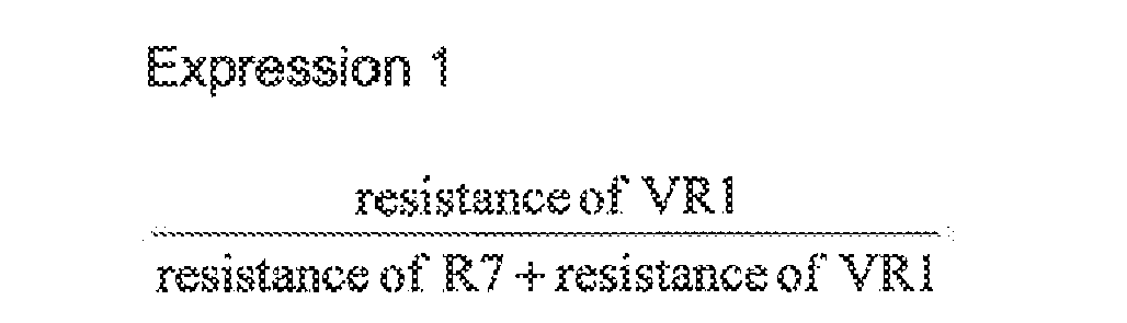
- The reference value applied to the non-inverting input terminal of the operational amplifier OP4 in the comparator 23-22 of the second comparison unit 23-2 is determined by the following
expression 2.
- Meanwhile, the first latch unit 25-1 latches an output value from the first comparison unit 23-1, and the second latch unit 25-2 latches an output value from the second comparison unit 23-2.
- The first and second latch units 25-1 and 25-2 function to store a signal informing that a fault is generated until they are reset.
- The fault signal output unit 27 outputs a fault signal informing that a fault current is generated according to the output values from the first and second latch units 25-1 and 25-2.
- A specific embodiment of the first and second latch units 25-1 and 25-2 respectively connected to the first and second comparison units 23-1 and 23-2 shown in
FIG. 2 will be described with reference toFIG. 3 . - In the embodiments shown in
FIG. 2 , the first and second comparison units 23-1 and 23-2 respectively output high digital signals when a fault current is generated, and the first and second latch units 25-1 and 25-2 may be configured using D latches 35-1 and 35-2. - A high signal is applied to a digital signal input terminal D of the D latch 35-1 in the first latch unit 25-1, and an output signal from the inverter 23-13 is inputted to a clock input terminal CP. An activation terminal IRD is connected to a switch unit 31-1 for determining the presence of activation of a latch operation.
- Therefore, if the output signal from the inverter 23-13 is changed from a low state to a high state, an output terminal Q of the D latch 35-1 at a rising edge becomes a high state.
- The switch unit 31-1 allows the user to determine the presence of the activation of the latch operation. If a low signal is inputted to the activation terminal IRD of the D latch 35-1, the latch operation is not activated. If a high signal is inputted to the activation terminal IRD of the D latch 35-1, the latch operation is activated.
- A high signal is applied to a digital signal input terminal D of the D latch 35-2 in the second latch unit 25-2, and an output signal from the inverter 23-23 is inputted to a clock input terminal CP. An activation terminal IRD is connected to a switch unit 31-2 for determining the presence of activation of a latch operation.
- Therefore, if the output signal from the inverter 23-23 is changed from a low state to a high state, an output terminal Q of the D latch 35-2 at a rising edge becomes a high state.
- The switch unit 31-2 allows the user to determine the presence of the activation of the latch operation. If a low signal is inputted to the activation terminal IRD of the D latch 35-2, the latch operation is not activated. If a high signal is inputted to the activation terminal IRD of the D latch 35-2, the latch operation is activated.
- In the embodiment described above, the first and second latch units 25-1 and 25-2 respectively output high signals when a fault is generated, and hence the fault signal output unit 27 may be configured as an AND gate element.
- That is, an AND gate element 27 outputs a fault signal when a fault is monitored from the AC current inputted from the current transformer 13 and the AC voltage inputted through the Rogowski coil 15.
- Meanwhile, a display unit 33-1 for turning on/off a light emitting diode (LED) according to the output value of the first latch unit 25-1 may be connected to the first latch unit 25-1 so that the user can visually identify the presence of occurrence of an accident.
- The embodiment shown in
FIG. 3 will be described. The display unit 33-1 may be configured in a structure in which a resistive element 37-1 for current limiting, an LED 37-2 and an inverter 37-3 are connected in series to one another. - If a high signal is outputted from the first latch unit 25-1 in the occurrence of an accident, an output terminal of the inverter 37-3 becomes a low state. Then, current flows from a power source to the LED 37-2 through the resistive element 37-1 for current limiting, and accordingly, the LED 37-2 is turned on.
- A display unit 33-2 for turning on/off an LED according to the output value of the second latch unit 25-2 may be connected to the second latch unit 25-2 so that the user can visually identify the presence of occurrence of an accident.
- The embodiment shown in
FIG. 3 will be described. The display unit 33-2 may be configured in a structure in which a resistive element 38-1 for current limiting, an LED 38-2 and an inverter 38-3 are connected in series to one another. - If a high signal is outputted from the second latch unit 25-2 in the occurrence of an accident, an output terminal of the inverter 38-3 becomes a low state. Then, current flows from a power source to the LED 38-2 through the resistive element 38-1 for current limiting, and accordingly, the LED 38-2 is turned on.
- A display unit 33-3 for turning on/off an LED according to the output value of the fault signal output unit 27 may be connected to the fault signal output unit 27 so that the user can visually identify the presence of occurrence of an accident.
- The embodiment shown in
FIG. 3 will be described. The display unit 33-3 may be configured in a structure in which a resistive element 39-1 for current limiting, an LED 39-2 and an inverter 39-3 are connected in series to one another, - If a high signal is outputted from the fault signal output unit 27 in the occurrence of an accident, an output terminal of the inverter 39-3 becomes a low state. Then, current flows from a power source to the LED 39-2 through the resistive element 39-1 for current limiting, and accordingly, the LED 39-2 is turned on.
- As described above, according to embodiments of the present invention, an AC signal detected from a power system is passed through a bridge diode, and in this state, the presence of occurrence of an accident is immediately determined. Thus, it is possible to prevent a response delay due to a rising time generated when the AC signal is smoothed to a DC signal through a capacitor and to quickly respond to the power system.
- The presence of occurrence of a fault in the power system is parallely monitored using a current transformer and a Rogowski coil. If a fault waveform is generated once, it is latched so that a corresponding state is maintained until a reset is performed. Then, a fault signal is outputted when the fault is monitored from the current transformer and the Rogowski coil.
- Accordingly, it is possible to prevent malfunction caused by chattering. Further, since a response can be quickly performed at the time when a fault current is generated for the first time, it is possible to be effectively applied to power system protection apparatuses such as a superconducting limiter, which require fast response characteristics.
- Although a few embodiments of the present invention have been shown and described, it would be appreciated by those skilled in the art that changes may be made in this embodiment without departing from the principles and spirit of the invention, the scope of which is defined in the claims and their equivalents.
Claims (8)
- An apparatus (20) for monitoring a fault current in a power system, the apparatus (20) characterized by:a first bridge diode (21-1) configured to receive an AC current detected from a distribution line (11) in the power system and full wave-rectify the received AC current;a second bridge diode (21-2) configured to receive an AC voltage detected from the distribution line (11) in the power system and full wave-rectify the received AC voltage;a first comparison unit (23-1) configured to convert a current signal outputted from the first bridge diode (21-1) into a voltage signal and output a high or low digital signal by comparing the converted voltage signal with a predetermined reference value;a second comparison unit (23-2) configured to output a high or low digital signal by comparing a voltage signal outputted from the second bridge diode (21-2) with a predetermined reference value;a first latch unit (25-1) configured to latch an output value of the first comparison unit;a second latch unit (25-2) configured to latch an output value of the second comparison unit; anda fault current output unit (27) configured to output a fault signal informing that a fault current is generated based on the output values of the first and second latch units (25-1, 25-2).
- The apparatus of claim 1, characterized in that the first comparison unit (23-1) comprises:a buffer (23-11) configured to convert the current signal outputted from the first bridge diode (21-1) into a voltage signal through a resistive element (R1-R4) for voltage conversion and output the converted voltage signal;a comparator (23-12) configured to receive the output signal of the buffer (23-11) and the reference value respectively through inverting and non-inverting input terminals of an operational amplifier (OP2) and output a high or low digital signal by comparing the output signal with the reference value; andan inverter (23-13) configured to invert the output signal of the comparator (23-12) and output the inverted signal.
- The apparatus of claim 2, characterized in that the first latch unit (25-1) comprises a D latch (35-1) having a digital signal input terminal to which a high signal is applied, a clock input terminal to which the output signal of the inverter (23-13) is inputted, and an activation terminal connected to a switch unit (31-1) that determines whether a latch operation is activated.
- The apparatus of claim 1, characterized in that the second comparison unit (23-2) comprises:a buffer (23-21) configured to receive a voltage signal outputted from the second bridge diode (21-2) and output the received voltage signal;a comparator (23-22) configured to receive the output signal of the buffer (23-21) and the reference value respectively through inverting and non-inverting input terminals of an operational amplifier (OP4) and output a high or low digital signal by comparing the output signal with the reference value; andan inverter (23-23) configured to invert the output signal of the comparator (23-22) and output the inverted signal.
- The apparatus of claim 4, characterized in that the second latch unit (25-2) comprises a D latch (35-2) having a digital signal input terminal to which a high signal is applied, a clock input terminal to which the output signal of the inverter (23-23) is inputted, and an activation terminal connected to a switch unit (31-2) that determines whether or not a latch operation is activated.
- The apparatus of claim 1, characterized in that the reference value is configured to be variably determined by a user using a variable resistive element (VR1 or VR2).
- The apparatus of claim 1, characterized by further comprising display units (33-1, 33-2) respectively connected to the first and second latch units (35-1, 35-2) so as to turn on/off light emitting diodes (LEDs) based on the output values thereof.
- The apparatus of claim 1, characterized by further comprising a display unit (33-3) connected to the fault signal output unit (27) so as to turn on/off an LED based on the output value thereof.
Applications Claiming Priority (1)
| Application Number | Priority Date | Filing Date | Title |
|---|---|---|---|
| KR1020100040941A KR101077768B1 (en) | 2010-04-30 | 2010-04-30 | Abnormal current monitoring device of power system |
Publications (1)
| Publication Number | Publication Date |
|---|---|
| EP2383581A1 true EP2383581A1 (en) | 2011-11-02 |
Family
ID=44477619
Family Applications (1)
| Application Number | Title | Priority Date | Filing Date |
|---|---|---|---|
| EP11163063A Withdrawn EP2383581A1 (en) | 2010-04-30 | 2011-04-19 | Apparatus for monitoring fault current in power system |
Country Status (4)
| Country | Link |
|---|---|
| US (1) | US20110267727A1 (en) |
| EP (1) | EP2383581A1 (en) |
| KR (1) | KR101077768B1 (en) |
| CN (1) | CN102243279B (en) |
Cited By (2)
| Publication number | Priority date | Publication date | Assignee | Title |
|---|---|---|---|---|
| EP3599691A1 (en) * | 2018-07-23 | 2020-01-29 | Smart Wires Inc. | Early detection of faults in power transmission lines |
| EP4212891A1 (en) * | 2022-01-08 | 2023-07-19 | Goodrich Aerospace Services Private Limited | Fault detection methods and systems therefor |
Families Citing this family (11)
| Publication number | Priority date | Publication date | Assignee | Title |
|---|---|---|---|---|
| KR101167448B1 (en) | 2010-12-16 | 2012-07-19 | 엘에스산전 주식회사 | Current Detection apparatus using sensor |
| CN102931648A (en) * | 2012-11-20 | 2013-02-13 | 合肥贝阿益电力设备有限公司 | Bus residual voltage holding device |
| US9735568B2 (en) | 2013-06-04 | 2017-08-15 | Suzhou Beiang Technology Ltd. | Ionic wind purifier and discharge monitoring and protective circuit of high-voltage ion purifier |
| CN103346548B (en) * | 2013-07-05 | 2015-11-25 | 苏州贝昂科技有限公司 | Electric discharge monitoring and protecting circuit in a kind of high-voltage ion purifier |
| CN103869213B (en) * | 2014-03-31 | 2016-05-04 | 常州机电职业技术学院 | Power line electrical on-off testing device |
| CN106208006A (en) * | 2016-08-28 | 2016-12-07 | 安徽普天电力科技有限公司 | A kind of transformator zero consumes degree of depth current-limiting method |
| CN106208002A (en) * | 2016-08-28 | 2016-12-07 | 安徽普天电力科技有限公司 | A kind of important load bus residual voltage keeping method |
| CN110429571B (en) * | 2019-07-04 | 2022-04-15 | 中国电力科学研究院有限公司 | Selectable-pole direct-current transmission line protection method and system |
| CN110488206B (en) * | 2019-08-13 | 2022-07-05 | 科华恒盛股份有限公司 | Fault monitoring system |
| CN113252966B (en) * | 2021-06-04 | 2024-11-05 | 广东福德电子有限公司 | A single-phase AC power supply signal detection circuit |
| CN113433481B (en) * | 2021-06-04 | 2024-11-01 | 广东福德电子有限公司 | Circuit for rapidly detecting single-phase alternating current power supply signal |
Citations (7)
| Publication number | Priority date | Publication date | Assignee | Title |
|---|---|---|---|---|
| US3671807A (en) * | 1970-12-07 | 1972-06-20 | Peripheral Systems Corp | Control apparatus |
| US3836854A (en) * | 1973-07-02 | 1974-09-17 | Lorain Prod Corp | Alarm circuit for monitoring the amplitude of a-c voltages |
| US4263635A (en) * | 1977-07-20 | 1981-04-21 | Steven Welk | Method and apparatus for sensing the clearance of fault current on an ac transmission line |
| US4362986A (en) * | 1980-10-14 | 1982-12-07 | Electric Power Research Institute, Inc. | Method and means for monitoring faults in an electric power system and the like |
| US4728898A (en) * | 1986-03-17 | 1988-03-01 | Staley Electric Co., Inc. | Method and apparatus for detecting and locating faults in an AC transmission line using two indicators |
| EP0286282A2 (en) * | 1987-03-27 | 1988-10-12 | Fuji Electrochemical Co.Ltd. | Method for detecting input ac voltage |
| JPH03279875A (en) * | 1990-03-29 | 1991-12-11 | Matsushita Electric Works Ltd | Fault detecting device |
Family Cites Families (20)
| Publication number | Priority date | Publication date | Assignee | Title |
|---|---|---|---|---|
| US4016468A (en) * | 1975-03-18 | 1977-04-05 | General Electric Company | Controlled rectifier motor drive system including d.c. fault detection and commutation means |
| US4200897A (en) * | 1978-05-15 | 1980-04-29 | Dawley Robert E | Ground leakage current interrupter |
| JPS5895923A (en) * | 1981-12-02 | 1983-06-07 | 三菱電機株式会社 | Overcurrent relay |
| US4775924A (en) * | 1987-02-27 | 1988-10-04 | Asea Power Systems, Inc. | Inverter commutation failure prevention method and apparatus |
| KR950020841A (en) * | 1993-12-29 | 1995-07-26 | 문정환 | Earth leakage breaker |
| US5568373A (en) * | 1994-07-28 | 1996-10-22 | Small; Kenneth T. | Tolerant power converter |
| KR100449959B1 (en) * | 1996-07-09 | 2004-12-08 | 후지 덴키 가부시끼가이샤 | Earth leakage breaker |
| JP3594562B2 (en) * | 2001-03-30 | 2004-12-02 | 三洋電機株式会社 | Power supply leakage detection circuit |
| EP1595150A1 (en) * | 2003-01-31 | 2005-11-16 | FMC Tech Limited | A monitoring device for a medium voltage overhead line |
| US7034515B2 (en) * | 2003-06-05 | 2006-04-25 | Mitsubishi Denki Kabushiki Kaisha | Instantaneous voltage lowering detection device |
| JP3966251B2 (en) * | 2003-08-08 | 2007-08-29 | オムロン株式会社 | DC current detection circuit and DC ground fault current detection circuit |
| KR100609266B1 (en) * | 2003-11-03 | 2006-08-04 | 삼성전자주식회사 | Fault detection method and circuit for performing the same, power amplifier circuit protection method according to fault, and power amplifier detecting fault |
| JP4215656B2 (en) | 2004-02-06 | 2009-01-28 | 北海道電力株式会社 | Ground fault detection device and ground fault detection method |
| US7535233B2 (en) * | 2004-07-15 | 2009-05-19 | Cooper Technologies Company | Traveling wave based relay protection |
| JP5214163B2 (en) | 2007-03-30 | 2013-06-19 | 北海道旅客鉄道株式会社 | Phase difference measurement system and phase difference measurement method |
| CN101424709B (en) * | 2007-10-29 | 2013-03-20 | 西门子公司 | Electric voltage disturbance detecting method and device |
| IS8689A (en) * | 2007-11-09 | 2009-05-10 | Hilmir Ingi Jonsson | Ground Terminal Block Fault Indicator |
| JP5349905B2 (en) * | 2008-10-27 | 2013-11-20 | パナソニック株式会社 | Discharge lamp lighting device and vehicle headlamp lighting device using the same |
| US8320089B1 (en) * | 2009-04-16 | 2012-11-27 | Musco Corporation | Apparatus, method, and system for integrating ground fault circuit interrupters in equipment-grounded high voltage systems |
| US8908338B2 (en) * | 2009-06-03 | 2014-12-09 | Siemens Industry, Inc. | Methods and apparatus for multi-frequency ground fault circuit interrupt grounded neutral fault detection |
-
2010
- 2010-04-30 KR KR1020100040941A patent/KR101077768B1/en not_active Expired - Fee Related
-
2011
- 2011-04-19 EP EP11163063A patent/EP2383581A1/en not_active Withdrawn
- 2011-04-20 US US13/091,030 patent/US20110267727A1/en not_active Abandoned
- 2011-04-29 CN CN2011101138941A patent/CN102243279B/en not_active Expired - Fee Related
Patent Citations (7)
| Publication number | Priority date | Publication date | Assignee | Title |
|---|---|---|---|---|
| US3671807A (en) * | 1970-12-07 | 1972-06-20 | Peripheral Systems Corp | Control apparatus |
| US3836854A (en) * | 1973-07-02 | 1974-09-17 | Lorain Prod Corp | Alarm circuit for monitoring the amplitude of a-c voltages |
| US4263635A (en) * | 1977-07-20 | 1981-04-21 | Steven Welk | Method and apparatus for sensing the clearance of fault current on an ac transmission line |
| US4362986A (en) * | 1980-10-14 | 1982-12-07 | Electric Power Research Institute, Inc. | Method and means for monitoring faults in an electric power system and the like |
| US4728898A (en) * | 1986-03-17 | 1988-03-01 | Staley Electric Co., Inc. | Method and apparatus for detecting and locating faults in an AC transmission line using two indicators |
| EP0286282A2 (en) * | 1987-03-27 | 1988-10-12 | Fuji Electrochemical Co.Ltd. | Method for detecting input ac voltage |
| JPH03279875A (en) * | 1990-03-29 | 1991-12-11 | Matsushita Electric Works Ltd | Fault detecting device |
Cited By (4)
| Publication number | Priority date | Publication date | Assignee | Title |
|---|---|---|---|---|
| EP3599691A1 (en) * | 2018-07-23 | 2020-01-29 | Smart Wires Inc. | Early detection of faults in power transmission lines |
| US10938314B2 (en) | 2018-07-23 | 2021-03-02 | Smart Wires Inc. | Early detection of faults in power transmission lines |
| EP4212891A1 (en) * | 2022-01-08 | 2023-07-19 | Goodrich Aerospace Services Private Limited | Fault detection methods and systems therefor |
| US12399231B2 (en) | 2022-01-08 | 2025-08-26 | Hamilton Sundstrand Corporation | Fault detection method and system therefor |
Also Published As
| Publication number | Publication date |
|---|---|
| KR101077768B1 (en) | 2011-10-27 |
| CN102243279A (en) | 2011-11-16 |
| CN102243279B (en) | 2013-12-11 |
| US20110267727A1 (en) | 2011-11-03 |
Similar Documents
| Publication | Publication Date | Title |
|---|---|---|
| KR101077768B1 (en) | Abnormal current monitoring device of power system | |
| US11009553B2 (en) | Fault detection for battery management systems | |
| CN103780064B (en) | Possesses the switching power source control circuit of secondary side feedback current detecting | |
| US20060186892A1 (en) | Open-phase detecting method and apparatus | |
| EP2867985B1 (en) | System for measuring soft starter current and method of making same | |
| CN216489729U (en) | Current-limiting protection circuit | |
| EP4075150B1 (en) | Leakage current detection circuit and fluxgate driver | |
| CN110161325B (en) | Voltage detection circuit | |
| KR101167448B1 (en) | Current Detection apparatus using sensor | |
| CN109217675A (en) | Power conversion device and its synchronous rectification circuit | |
| WO2016024490A1 (en) | Charging device | |
| JP6320210B2 (en) | Power supply | |
| CN105391320B (en) | Polyphase source circuit | |
| US7072160B1 (en) | Monitoring device for power supplies | |
| CN109698619A (en) | Load driving circuits and device | |
| CN219609051U (en) | Battery voltage detection circuit and electronic equipment | |
| CN119310332A (en) | An inductive current measurement circuit with automatic range switching and a current measurement method | |
| CN112114543A (en) | An AC circuit breaker controller | |
| EP4064718B1 (en) | State detection apparatus | |
| CN111323691A (en) | Detection circuit and diagnosis method of pulse width modulation circuit | |
| KR102309483B1 (en) | Apparatus for detecting whether power is supplied abnormally | |
| JP6271100B1 (en) | Digital relay | |
| CN114252803A (en) | Power electronic device short-circuit fault pre-detection circuit for bridge converter | |
| JP4851183B2 (en) | Capacitor input type rectifier circuit having overcurrent detection function and inverter device using the same | |
| CN219960097U (en) | Protection circuit, integrated circuit and electronic equipment |
Legal Events
| Date | Code | Title | Description |
|---|---|---|---|
| AK | Designated contracting states |
Kind code of ref document: A1 Designated state(s): AL AT BE BG CH CY CZ DE DK EE ES FI FR GB GR HR HU IE IS IT LI LT LU LV MC MK MT NL NO PL PT RO RS SE SI SK SM TR |
|
| AX | Request for extension of the european patent |
Extension state: BA ME |
|
| PUAI | Public reference made under article 153(3) epc to a published international application that has entered the european phase |
Free format text: ORIGINAL CODE: 0009012 |
|
| 17P | Request for examination filed |
Effective date: 20120502 |
|
| STAA | Information on the status of an ep patent application or granted ep patent |
Free format text: STATUS: THE APPLICATION HAS BEEN WITHDRAWN |
|
| 18W | Application withdrawn |
Effective date: 20160908 |