EP2381572B1 - Verwendung von trench-mos-barrier-schottky-dioden (tmbs) als gleichrichtende elemente einer gleichrichter-brückenschaltung eines kraftfahrzeuggenerators - Google Patents
Verwendung von trench-mos-barrier-schottky-dioden (tmbs) als gleichrichtende elemente einer gleichrichter-brückenschaltung eines kraftfahrzeuggenerators Download PDFInfo
- Publication number
- EP2381572B1 EP2381572B1 EP11156122.1A EP11156122A EP2381572B1 EP 2381572 B1 EP2381572 B1 EP 2381572B1 EP 11156122 A EP11156122 A EP 11156122A EP 2381572 B1 EP2381572 B1 EP 2381572B1
- Authority
- EP
- European Patent Office
- Prior art keywords
- diodes
- tmbs
- breakdown
- trench
- voltage
- Prior art date
- Legal status (The legal status is an assumption and is not a legal conclusion. Google has not performed a legal analysis and makes no representation as to the accuracy of the status listed.)
- Active
Links
Images

Classifications
-
- H—ELECTRICITY
- H02—GENERATION; CONVERSION OR DISTRIBUTION OF ELECTRIC POWER
- H02M—APPARATUS FOR CONVERSION BETWEEN AC AND AC, BETWEEN AC AND DC, OR BETWEEN DC AND DC, AND FOR USE WITH MAINS OR SIMILAR POWER SUPPLY SYSTEMS; CONVERSION OF DC OR AC INPUT POWER INTO SURGE OUTPUT POWER; CONTROL OR REGULATION THEREOF
- H02M7/00—Conversion of AC power input into DC power output; Conversion of DC power input into AC power output
- H02M7/02—Conversion of AC power input into DC power output without possibility of reversal
- H02M7/04—Conversion of AC power input into DC power output without possibility of reversal by static converters
- H02M7/06—Conversion of AC power input into DC power output without possibility of reversal by static converters using discharge tubes without control electrode or semiconductor devices without control electrode
-
- H—ELECTRICITY
- H10—SEMICONDUCTOR DEVICES; ELECTRIC SOLID-STATE DEVICES NOT OTHERWISE PROVIDED FOR
- H10D—INORGANIC ELECTRIC SEMICONDUCTOR DEVICES
- H10D8/00—Diodes
- H10D8/60—Schottky-barrier diodes
- H10D8/605—Schottky-barrier diodes of the trench conductor-insulator-semiconductor barrier type, e.g. trench MOS barrier Schottky rectifiers [TMBS]
Definitions
- the invention relates to a use of trench MOS-barrier Schottky diodes (TMBS) as rectifying elements of a rectifier bridge circuit of a motor vehicle generator.
- TMBS trench MOS-barrier Schottky diodes
- AC generators use AC bridges for rectification.
- B6 bridges are used in 3-phase three-phase systems, which contain six pn semiconductor diodes made of silicon as rectifying elements. Such a B6 bridge is in the FIG. 1 shown.
- the semiconductor diodes are usually designed as Z-diodes.
- alternators with a different number of phases are used.
- the bridges used as rectifiers are then constructed accordingly.
- a complete generator system also contains a voltage regulator which ensures that the rectified voltage has a specific value, for example 14.3 V.
- a suppression capacitor of 2.2 ⁇ F for example, is connected between B + and ground. Regulator, alternator and capacitor are in the FIG. 1 not shown.
- the Zener diodes are designed for operation at high currents in the flow direction, with current densities up to about 500 A / cm 2 , and at high temperatures.
- the voltage drop in the flow direction, the forward voltage UF, at the high currents used is about 1 volt.
- Reverse direction When operating in Reverse direction, however, only a very small reverse current IR flows up to a breakdown voltage UZ. From this voltage, the reverse current increases very strongly. A further increase in voltage is therefore prevented.
- the breakdown voltages of the Zener diodes are in the case of a 12 V electrical system above the generator voltage in a range of about 19-26 V.
- the Zener diodes are designed so that they can be briefly subjected to very high currents in the breakthrough. They thereby protect the on-board network and the regulator against overvoltages in the event of a sudden increase in generator voltage, by limiting the generator voltage.
- the generator voltage increases in sudden load changes particularly strong when a large load change occurs with not connected or defective battery (load dump).
- the controller When the controller detects the voltage increase, it shuts off the excitation current. However, since the magnetic field of the field winding does not abruptly disappear, the increased generator voltage sounds only relatively slowly with a time duration of about 100-400 ms.
- the generator voltage UB + measured at terminal B + is limited to UZ - UF.
- the one terminal of the diodes is led out as a connection wire, while the other connection consists of a round metal base, which is pressed into an existing bore of a cooling plate of the rectifier and ensures good thermal and electrical connection.
- the double-sided thermal connection acts as heat capacity and effectively buffers the temperature increase in the load dump.
- the breakdown voltages of all Zener diodes in the bridge are identical, at least if all diodes have the same temperature before the load dump.
- a certain relief can be caused by the temperature behavior of the breakdown voltage, since the breakdown voltage in Z diodes increases with increasing temperature (positive temperature coefficient).
- the diode with the lowest breakdown voltage UZ When inserting a load dump, the diode with the lowest breakdown voltage UZ first enters breakthrough. More current flows through this diode than through the other diodes. As a result, it heats up more and equalizes your breakdown voltage UZ something of that of the other diodes. However, this effect is usually not sufficient to set completely symmetrical current and voltage distributions.
- Rectifier arrangements with trench MOS-barrier Schottky diodes are known in which Z-diodes or integrated pn junctions are introduced as additional protection elements for operation in the breakdown.
- TMBS Diodes Challenge Planar Schottky's, "Max Chen et al., Describes the use of TMBS diodes in switching rectifiers.
- the invention relates to a use of trench MOS-barrier Schottky diodes (TMBS) as rectifying elements of a rectifier bridge circuit of a motor vehicle generator according to claim 1.
- TMBS trench MOS-barrier Schottky diodes
- Such a rectifier bridge circuit has as rectifying elements instead of the usual Z-diodes elements in which the breakdown voltage UZ increases during operation in the breakthrough. This achieves identical breakdown voltages of the diodes in the rectifier, even if the breakdown voltages of the diodes differ before operation are. In the case of a load dump, the load dump energy is distributed evenly across all diodes, maximizing the achievable load dump energy.
- a clamping element a structure in which the breakdown voltage increases during operation in the breakdown.
- a metal-oxide semiconductor structure is preferably used.
- TMBS trench MOS-barrier Schottky diode
- This arrangement also has the advantage that the forward voltage can be set lower than with pn diodes. For example, a forward voltage between 0.5 V and 0.7 V at 500 A / cm 2 can be achieved.
- the FIG. 2 shows as a first embodiment realized as a chip TMBS consisting of an n + substrate 1, an n-epi layer 2, at least two realized in the n-epi layer 2 by etching trenches (6), metal layers on the front side 4 of the chip as the anode electrode and at the back 5 of the chip as the cathode electrode, and oxide layers 7 between the trenches 6 and the metal layers.
- the TMBS is a combination of a MOS structure (metal layer, oxide layers 7 and n epilayer 2) and a Schottky diode (Schottky barrier between the metal layer as the anode and the n-epi layer 2 as the cathode).
- TMBS In the direction of flow, currents flow through the mesa area between the trenches 6.
- the trenches 6 themselves are not available for the flow of current.
- a TMBS has very low reverse currents.
- space charge zones are formed in both the MOS structure and the Schottky diode.
- the space charge zones expand with increasing voltage and collide in the middle of the area between the adjacent trenches 6 at a voltage lower than the breakdown voltage of the TMBS. This shields the high blocking currents responsible for Schottky effects and reduces the reverse currents.
- This shielding effect is strongly dependent on structure parameters Dt (depth of the trench), Wm (distance between the trenches), Wt (width of the trench) and To (thickness of the oxide layer).
- the trenches 6 are introduced by etching the n-epilayer 2, growing the oxide layer 7 and filling the trenches with conductive, doped layers of polysilicon.
- the trenches can be filled with metal.
- the expansion of the space charge zones in the mesa region between the trenches 6 is quasi-one-dimensional, provided that the depth Dt of the trench is significantly greater than the distance Wm between the trenches.
- nickel or nickel silicide is used on the front side 4 of the chip for the Schottky metal.
- This makes it possible to set low flux voltages in the range of 0.5 V - 0.7 V with simultaneously low reverse currents. It has been found to be advantageous that TMBS structures can be operated at high currents in the breakdown, without causing the diode to be destroyed.
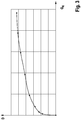
- the blocking voltage drifts upward, with the increase in voltage decreasing over time. This is in the FIG. 3 1, which illustrates the behavior of the voltage drift D of a TMBS as a function of the cumulative breakdown charge Q K.
- the cumulative breakdown charge arises with increasing time in breakthrough operation with decreasing breakdown power UZ * IZ.
- Another embodiment of a combination of a rectifying structure and a trench MOS structure showing voltage drift in the breakdown is to insert a p-layer between metal on the front side 4 and n-type silicon 2 in FIG. 2 whose breakdown voltage UZPN is greater is considered the breakdown voltage of the MOS structure UZMOS.
- planar distributed planar MOS structures can also be used, wherein the reverse voltage breakdown occurs again at the MOS structure.
- a rectifier bridge circuit according to the present invention can be used in particular in recuperation mode AC generators.
Landscapes
- Engineering & Computer Science (AREA)
- Power Engineering (AREA)
- Electrodes Of Semiconductors (AREA)
- Rectifiers (AREA)
Description
- Die Erfindung betrifft eine Verwendung von Trench-MOS-Barrier-Schottky-Dioden (TMBS) als gleichrichtende Elemente einer Gleichrichter-Brückenschaltung eines Kraftfahrzeuggenerators.
- Bei Wechselstromgeneratoren (Lichtmaschinen) werden zur Gleichrichtung Wechselstrombrücken verwendet. Beispielsweise werden bei 3-phasigen Drehstromsystemen sogenannte B6-Brücken verwendet, die als gleichrichtende Elemente sechs pn-Halbleiterdioden aus Silizium enthalten. Eine derartige B6-Brücke ist in der
Figur 1 dargestellt. Die Halbleiterdioden werden üblicherweise als Z-Dioden ausgelegt. Neben 3-phasigen Systemen werden auch Wechselstromgeneratoren mit einer anderen Phasenzahl verwendet. Die als Gleichrichter verwendeten Brücken sind dann entsprechend aufgebaut. Ein komplettes Generatorsystem enthält neben dem Generator und der Wechselstrombrücke noch einen Spannungsregler, der dafür sorgt, dass die gleichgerichtete Spannung einen bestimmten Wert, beispielsweise 14,3 V, aufweist. Außerdem ist noch ein Entstörkondensator von beispielsweise 2,2 µF zwischen B+ und Masse geschaltet. Regler, Drehstromgenerator und Kondensator sind in derFigur 1 nicht eingezeichnet. - Die Z-Dioden sind für den Betrieb bei hohen Strömen in Flussrichtung, wobei Stromdichten bis etwa 500 A/cm2 auftreten, und bei hohen Temperaturen ausgelegt. Typischerweise beträgt der Spannungsabfall in Flussrichtung, die Flussspannung UF, bei den verwendeten hohen Strömen ca. 1 Volt. Bei Betrieb in Sperrrichtung fließt dagegen nur ein sehr kleiner Sperrstrom IR bis zu einer Durchbruchsspannung UZ. Ab dieser Spannung steigt der Sperrstrom sehr stark an. Ein weiterer Spannungsanstieg wird deshalb verhindert.
- Die Durchbruchsspannungen der Z-Dioden liegen im Fall eines 12 V Bordnetzes oberhalb der Generatorspannung in einem Bereich von etwa 19-26 V. Die Z-Dioden sind so ausgelegt, dass sie kurzzeitig mit sehr hohen Strömen im Durchbruch belastet werden können. Sie bieten dadurch einen Schutz des Bordnetzes und des Reglers gegen Überspannungen bei plötzlich ansteigender Generatorspannung, indem sie die Generatorspannung begrenzen. Die Generatorspannung steigt bei plötzlichen Lastwechseln dann besonders stark an, wenn ein großer Lastwechsel bei nicht angeschlossener oder defekter Batterie auftritt (Loaddump).
- Im Fall eines Loaddumps steigt die Spannung an den Phasen des Generators an, bis die Durchbruchsspannungen der Z-Dioden erreicht sind. Für die Differenz zwischen zwei Phasenspannungen gilt: Strangspannung = UF + UZ. Der Strom fließt dann als Durchbruchsstrom über die Z-Dioden, die sich gerade in Sperrrichtung befinden. Dabei ist immer eine Diode in Flussrichtung und eine Diode in Durchbruchsrichtung in Reihe geschaltet. Im Fall der B6-Brücke teilt sich der Generatorstrom üblicherweise so auf, dass er beispielsweise von einer Plusdiode und zwei Minusdioden in Durchbruchsrichtung getragen wird und in der folgenden Phase von zwei Plusdioden und einer Minusdiode. Im Extremfall, wenn eine Phase Null ist, befindet sich eine Plus- und eine Minusdiode im Durchbruch. Wenn der Regler den Spannungsanstieg erkennt, schaltet er den Erregerstrom ab. Da das Magnetfeld der Erregerwicklung aber nicht schlagartig verschwindet, klingt die erhöhte Generatorspannung nur relativ langsam mit einer Zeitdauer von ca. 100-400 ms ab. Die an der Klemme B+ gemessene Generatorspannung UB+ wird auf UZ - UF begrenzt.
- Während eines Loaddumps fließen sehr hohe Durchbruchsströme durch die Dioden. Im Fall eines vollen Loaddumps, d. h. eines vollständigen Batterie- und Lastabwurfes, wird der gesamte Generatorstrom von den Dioden im Durchbruch übernommen. Die Energie UZ * IZ wird in den Dioden in Wärme umgewandelt. Deshalb steigt die Junctiontemperatur Tj der Dioden kurzzeitig stark an. Üblicherweise werden für diese Ereignisse Temperaturen Tj weit oberhalb der maximal zulässigen Dioden-Betriebstemperatur spezifiziert. Um den Temperaturanstieg abzupuffern werden die Z-Dioden in Einpressdiodengehäuse verpackt, wie es beispielsweise in der
DE 102 42 521 A1 beschrieben ist. Dabei ist der eine Anschluss der Dioden als Anschlussdraht herausgeführt, während der andere Anschluss aus einem runden Metallsockel besteht, der in eine vorhandene Bohrung einer Kühlplatte des Gleichrichters eingepresst wird und für eine gute thermische und elektrische Verbindung sorgt. Die beidseitige thermische Anbindung wirkt als Wärmekapazität und puffert den Temperaturanstieg im Loaddump effektiv ab. - Idealerweise sind die Durchbruchsspannungen aller Z-Dioden in der Brücke identisch, zumindest sofern alle Dioden vor dem Loaddump dieselbe Temperatur aufweisen.
- Für den Fall identischer Durchbruchsspannungen fällt an den Dioden kurzzeitig maximal der halbe Generatorstrom ab. Wegen unvermeidbarer Fertigungsschwankungen sind jedoch nicht alle Z-Spannungen UZ der Dioden innerhalb eines Gleichrichters identisch. Dies führt zu ungleichmäßigen Belastungen der Dioden im Durchbruch und damit zu einer insgesamt reduzierten Loaddumpfestigkeit des Generators.
- Eine gewisse Entlastung kann durch das Temperaturverhalten der Durchbruchsspannung bewirkt werden, da die Durchbruchsspannung bei Z-Dioden mit zunehmender Temperatur ansteigt (positiver Temperaturkoeffizient).
- Beim Einsetzen eines Loaddumps gerät die Diode mit der niedrigsten Durchbruchsspannung UZ zuerst in den Durchbruch. Es fließt mehr Strom durch diese Diode als durch die weiteren Dioden. Dadurch heizt sie sich stärker auf und gleicht Ihre Durchbruchsspannung UZ etwas an die der anderen Dioden an. Allerdings ist dieser Effekt meist nicht ausreichend, um völlig symmetrische Strom- und Spannungsverteilungen einzustellen.
- Aus der
DE 10 2004 056 663 A1 sind Gleichrichteranordnungen mit Trench-MOS-Barrier-Schottky-Dioden (TMBS) bekannt, in welche als zusätzliche Schutzelemente für den Betrieb im Durchbruch Z-Dioden oder integrierte pn-Übergänge eingebracht sind. - In "High-Voltage TMBS Diodes Challenge Planar Schottkys", "Max Chen et al., wird die Verwendung von TMBS-Dioden in Schaltgleichrichtern beschrieben.
- Die Erfindung betrifft eine Verwendung von Trench-MOS-Barrier-Schottky-Dioden (TMBS) als gleichrichtende Elemente einer Gleichrichter-Brückenschaltung eines Kraftfahrzeuggenerators gemäß Anspruch 1.
- Eine solche Gleichrichter-Brückenschaltung weist als gleichrichtende Elemente statt der üblichen Z-Dioden Elemente auf, bei denen sich die Durchbruchsspannung UZ bei Betrieb im Durchbruch erhöht. Dadurch erreicht man identische Durchbruchsspannungen der Dioden im Gleichrichter, selbst wenn die Durchbruchsspannungen der Dioden vor dem Betrieb unterschiedlich
sind. Im Fall eines Loaddumps wird die Loaddumpenergie gleichmäßig auf alle Dioden verteilt und damit die erzielbare Loaddumpenergie maximiert. - Insbesondere werden anstelle von einfachen Z-Dioden in Gleichrichtern, die im Wesentlichen eine pn-Halbleiterstruktur darstellen, Elemente vorgeschlagen, die als Klammerelement eine Struktur verwenden, bei der sich die Durchbruchsspannung beim Betrieb im Durchbruch erhöht. Als Klammerelement wird vorzugsweise eine Metall-Oxid-Halbleiterstruktur verwendet. Für den Einsatz im Gleichrichter wird als besonders vorteilhaft eine Trench-MOS-Barrier-Schottky-Diode (TMBS) - also eine Kombination von Schottky-Diode und Trench-MOS-Struktur - vorgeschlagen. Diese Anordnung hat daneben noch den Vorteil, dass die Flussspannung niedriger als bei pn-Dioden eingestellt werden kann. Beispielsweise kann eine Flussspannung zwischen 0,5 V und 0,7 V bei 500 A/cm2 erreicht werden.
- Die
Figur 2 zeigt als ein erstes Ausführungsbeispiel eine als Chip realisierte TMBS bestehend aus einem n+-Substrat 1, einer n-Epischicht 2, mindestens zwei in der n-Epischicht 2 durch Ätzen realisierte Gräben (Trenchs) 6, Metallschichten an der Vorderseite 4 des Chips als Anodenelektrode und an der Rückseite 5 des Chips als Kathodenelektrode, und Oxidschichten 7 zwischen den Gräben 6 und den Metallschichten. Elektrisch gesehen ist die TMBS eine Kombination von einer MOS-Struktur (Metallschicht, Oxidschichten 7 und n-Epischicht 2) und einer Schottky-Diode (Schottky-Barriere zwischen der Metallschicht als Anode und der n-Epischicht 2 als Kathode). - In Flussrichtung fließen Ströme durch den Mesa-Bereich zwischen den Gräben 6. Die Gräben 6 selbst stehen für den Stromfluss nicht zur Verfügung. Eine TMBS weist sehr niedrige Sperrströme auf. In der Sperrrichtung bilden sich sowohl bei der MOS-Struktur als auch bei der Schottky-Diode Raumladungszonen aus. Die Raumladungszonen dehnen sich mit steigender Spannung aus und stoßen bei einer Spannung, die kleiner als die Durchbruchspannung der TMBS ist, in der Mitte des Bereichs zwischen den benachbarten Gräben 6 zusammen. Dadurch werden die für hohe Sperrströme verantwortlichen Schottky-Effekte abgeschirmt und die Sperrströme reduziert. Dieser Abschirmeffekt ist stark von Strukturparametern Dt (Tiefe des Grabens), Wm (Abstand zwischen den Gräben), Wt (Breite des Grabens) sowie von To (Dicke der Oxidschicht) abhängig.
- Im Rahmen der Herstellung einer TMBS erfolgt ein Einbringen der Gräben 6 durch Ätzen der n-Epischicht 2, Wachsen der Oxidschicht 7 und Ausfüllen der Gräben mit leitfähigen, dotierten Schichten aus Polysilizium. Alternativ können die Gräben mit Metall gefüllt werden. Die Ausdehnung der Raumladungszonen im Mesa-Bereich zwischen den Gräben 6 ist quasi-eindimensional, sofern die Tiefe Dt des Grabens deutlich größer als der Abstand Wm zwischen den Gräben ist.
- Beim Sperrspannungsdurchbruch entstehen sehr hohe elektrische Felder innerhalb der Oxidschicht 7 in der Nähe des Trenchbodens und direkt in der Nähe der Oxidschicht in der n-Epischicht 2. Als Folge werden beim Sperrspannungs- oder Avalance-Durchbruch heiße Ladungsträger von der n-Epischicht 2 in die Oxidschicht 7 der MOS-Struktur injiziert. In der gezeigten Anordnung mit einer n-dotierten Epischicht 2 handelt es sich um Löcher. Als Folge dieses Prozesses verbleiben positive Ladungen in der Oxidschicht und schirmen das von außen angelegte elektrische Feld der Sperrspannung ab. Um die Durchbruchfeldstärke im Silizium zu erreichen wird deshalb ein höheres externes Feld bzw. eine höhere externe Spannung benötigt. Die Durchbruchsspannung der TMBS-Struktur steigt an.
- In besonders vorteilhafter Weise wird für das Schottky-Metall an der Vorderseite 4 des Chips Nickel oder Nickelsilizid verwendet. Dadurch gelingt es niedrige Flussspannungen im Bereich von 0,5 V - 0,7 V bei gleichzeitig niedrigen Sperrströmen einzustellen. Es hat sich in vorteilhafter Weise gezeigt, dass TMBS-Strukturen bei hohen Strömen im Durchbruch betrieben werden können, ohne dass es zu einer Zerstörung der Diode kommt. Die Sperrspannung driftet dabei nach oben, wobei die Zunahme der Spannung mit der Zeit abnimmt. Dies ist in der
Figur 3 veranschaulicht, in welcher das Verhalten der Spannungsdrift D einer TMBS in Abhängigkeit von der kumulierten Durchbruchsladung QK veranschaulicht ist. Die kumulierte Durchbruchsladung entsteht mit zunehmender Zeit im Durchbruchsbetrieb bei abfallender Durchbruchsleistung UZ * IZ. - Werden nun beispielsweise in einer B6-Brücke gemäß
Fig.1 die Dioden ZD1 bis ZD6 durch TMBS-Dioden gemäßFig.2 , die ein Driftverhalten der Sperrspannung gemäßFig.3 zeigen, ersetzt, dann gleichen sich die Durchbruchsspannungen der TMBS-Dioden bei Betrieb im Durchbruch an. Die Loaddumpfestigkeit eines Kraftfahrzeuggenerators, von welchem die Gleichrichter-Brückenschaltung Bestandteil ist, wird erhöht. Natürlich können auch Gleichrichter für Wechselstromgeneratoren mit mehr als drei Phasen, z.B. mit 5, 6 oder 7 Phasen, mit Elementen gemäß derFigur 2 bestückt werden. Wie Loaddump-Messungen an Generatoren zeigen, kann etwa 20% mehr Loaddumpstrom abgeschaltet werden. - Ein weiteres Ausführungsbeispiel für eine Kombination einer gleichrichtenden Struktur und einer Trench-MOS-Struktur, die Spannungsdrift im Durchbruch zeigt, besteht darin, zwischen Metall an der Vorderseite 4 und n-Silizium 2 in Figur 2 eine p-Schicht einzufügen, deren Durchbruchsspannung UZPN größer ist als die Durchbruchsspannung der MOS-Struktur UZMOS.
- Des Weiteren können anstelle der Trench-MOS-Strukturen auch flächig verteilte planare MOS-Strukturen verwendet werden, wobei der Sperrspannungsdurchbruch wieder an der MOS-Struktur stattfindet.
- Eine Gleichrichter-Brückenschaltung gemäß der vorliegenden Erfindung kann insbesondere in Wechselstromgeneratoren mit Rekuperationsbetrieb verwendet werden.
Claims (6)
- Verwendung von Trench-MOS-Barrier-Schottky-Dioden (TMBS) als gleichrichtende Elemente einer Gleichrichter-Brückenschaltung eines Kraftfahrzeuggenerators, die eine Drift der Sperrspannung aufweisen, wenn sie im Durchbruch betrieben werden, wobei die Trench-MOS-Barrier-Schottky-Dioden (TMBS)bei Betrieb im Durchbruch die Durchbruchspannung UZ erhöhen, wobei sich die Durchbruchsspannungen der Trench-MOS-Barrier-Schottky-Dioden (TMBS) bei Betrieb der Gleichrichter-Brückenschaltung im Durchbruch angleichen.
- Verwendung nach Anspruch 1, dadurch gekennzeichnet, dass es sich bei den gleichrichtenden Elementen um Trench-MOS-Barrier-Schottky-Dioden (TMBS) mit einer Schottky-Barriere von etwa 0,65 eV bis 0,7 eV handelt.
- Verwendung nach einem der vorhergehenden Ansprüche, dadurch gekennzeichnet, dass es sich bei den gleichrichtenden Elementen um Trench-MOS-Barrier-Schottky-Dioden (TMBS) mit einem Schottky-Barrierenmetall aus Nickel oder Nickelsilizid handelt.
- Verwendung nach einem der vorhergehenden Ansprüche, dadurch gekennzeichnet, dass es sich bei den gleichrichtenden Elementen um Trench-MOS-Barrier-Schottky-Dioden (TMBS) handelt, bei denen die Gräben etwa 1 - 3 µm und der Abstand von Graben zu Graben etwa 0,5 - 1 µm beträgt.
- Verwendung nach einem der vorhergehenden Ansprüche, dadurch gekennzeichnet, dass die MOS-Strukturen gleichmäßig über einen Chip verteilt angeordnet sind.
- Verwendung nach einem der vorhergehenden Ansprüche, dadurch gekennzeichnet, dass mindestens eines der gleichrichtenden Elemente als Einpressdiode ausgeführt ist.
Applications Claiming Priority (1)
| Application Number | Priority Date | Filing Date | Title |
|---|---|---|---|
| DE102010028203A DE102010028203A1 (de) | 2010-04-26 | 2010-04-26 | Gleichrichter-Brückenschaltung |
Publications (2)
| Publication Number | Publication Date |
|---|---|
| EP2381572A1 EP2381572A1 (de) | 2011-10-26 |
| EP2381572B1 true EP2381572B1 (de) | 2019-05-08 |
Family
ID=44455290
Family Applications (1)
| Application Number | Title | Priority Date | Filing Date |
|---|---|---|---|
| EP11156122.1A Active EP2381572B1 (de) | 2010-04-26 | 2011-02-28 | Verwendung von trench-mos-barrier-schottky-dioden (tmbs) als gleichrichtende elemente einer gleichrichter-brückenschaltung eines kraftfahrzeuggenerators |
Country Status (5)
| Country | Link |
|---|---|
| EP (1) | EP2381572B1 (de) |
| JP (1) | JP2011234614A (de) |
| DE (1) | DE102010028203A1 (de) |
| ES (1) | ES2738554T3 (de) |
| HU (1) | HUE045291T2 (de) |
Families Citing this family (2)
| Publication number | Priority date | Publication date | Assignee | Title |
|---|---|---|---|---|
| DE102012207654A1 (de) | 2012-05-08 | 2013-11-14 | Robert Bosch Gmbh | Kraftfahrzeug-Generatorvorrichtung mit einer Schutzanordnung zur Störsignalunterdrückung |
| US9842836B2 (en) | 2015-04-14 | 2017-12-12 | Rohm Co., Ltd. | Diode |
Citations (2)
| Publication number | Priority date | Publication date | Assignee | Title |
|---|---|---|---|---|
| WO2001011693A1 (en) * | 1999-08-10 | 2001-02-15 | Rockwell Science Center, Llc | High power rectifier |
| DE102004053760A1 (de) * | 2004-11-08 | 2006-05-11 | Robert Bosch Gmbh | Halbleitereinrichtung und Verfahren für deren Herstellung |
Family Cites Families (9)
| Publication number | Priority date | Publication date | Assignee | Title |
|---|---|---|---|---|
| JPH0233976A (ja) * | 1988-07-22 | 1990-02-05 | Mitsubishi Electric Corp | ツェナーダイオード |
| JP2879479B2 (ja) * | 1991-04-19 | 1999-04-05 | 新電元工業株式会社 | ショットキバリア半導体装置 |
| DE10009171B4 (de) * | 2000-02-26 | 2005-08-11 | Robert Bosch Gmbh | Stromrichter und sein Herstellverfahren |
| JP3943322B2 (ja) * | 2000-11-07 | 2007-07-11 | 松下電器産業株式会社 | 半導体装置 |
| US6580141B2 (en) * | 2001-06-01 | 2003-06-17 | General Semiconductor, Inc. | Trench schottky rectifier |
| DE10242521A1 (de) | 2002-09-12 | 2004-03-25 | Robert Bosch Gmbh | Diode |
| DE102004056663A1 (de) * | 2004-11-24 | 2006-06-01 | Robert Bosch Gmbh | Halbleitereinrichtung und Gleichrichteranordnung |
| FR2880193A1 (fr) * | 2004-12-23 | 2006-06-30 | St Microelectronics Sa | Diode schottky a barriere verticale |
| EP2320465A4 (de) * | 2008-08-05 | 2014-01-22 | Sumitomo Electric Industries | Schottky-diode und herstellungsverfahren für eine schottky-diode |
-
2010
- 2010-04-26 DE DE102010028203A patent/DE102010028203A1/de not_active Withdrawn
-
2011
- 2011-02-28 EP EP11156122.1A patent/EP2381572B1/de active Active
- 2011-02-28 ES ES11156122T patent/ES2738554T3/es active Active
- 2011-02-28 HU HUE11156122A patent/HUE045291T2/hu unknown
- 2011-04-26 JP JP2011098258A patent/JP2011234614A/ja active Pending
Patent Citations (2)
| Publication number | Priority date | Publication date | Assignee | Title |
|---|---|---|---|---|
| WO2001011693A1 (en) * | 1999-08-10 | 2001-02-15 | Rockwell Science Center, Llc | High power rectifier |
| DE102004053760A1 (de) * | 2004-11-08 | 2006-05-11 | Robert Bosch Gmbh | Halbleitereinrichtung und Verfahren für deren Herstellung |
Non-Patent Citations (1)
| Title |
|---|
| MAX CHEN ET AL: "High-Voltage TMBS Diodes Challenge Planar Schottkys", 31 October 2006 (2006-10-31), pages 22 - 32, XP055128222, Retrieved from the Internet <URL:http://powerelectronics.com/mag/610PET21.pdf> [retrieved on 20140710] * |
Also Published As
| Publication number | Publication date |
|---|---|
| DE102010028203A1 (de) | 2011-10-27 |
| HUE045291T2 (hu) | 2019-12-30 |
| JP2011234614A (ja) | 2011-11-17 |
| EP2381572A1 (de) | 2011-10-26 |
| ES2738554T3 (es) | 2020-01-23 |
Similar Documents
| Publication | Publication Date | Title |
|---|---|---|
| EP1812970B1 (de) | Halbleitereinrichtung und verfahren für deren herstellung | |
| EP2976787B1 (de) | Gleichrichterdiode | |
| DE102018132111B4 (de) | Siliciumcarbid-Halbleitervorrichtung und Verfahren zu ihrer Herstellung | |
| DE112011102926T5 (de) | Halbleiterbauteil | |
| DE102015118165A1 (de) | Elektrische baugruppe, umfassend eine halbleiterschaltvorrichtung und eine klemmdiode | |
| EP1817799B1 (de) | Halbleiterbauelement und gleichrichteranordnung | |
| DE102009028252A1 (de) | Halbleiteranordnung | |
| DE102010062677A1 (de) | Generatorvorrichtung zur Spannungsversorgung eines Kraftfahrzeugs | |
| EP2462620B1 (de) | Halbleiteranordnung und verfahren zu deren herstellung | |
| EP1825520B1 (de) | Halbleitereinrichtung und verfahren zu deren herstellung | |
| DE102011003961A1 (de) | Trench-Schottkydiode | |
| DE112020006718T5 (de) | Verfahren zur herstellung einer siliciumcarbid-halbleitereinheit und leistungswandlereinheit unter verwendung der siliciumcarbid-halbleitereinheit | |
| DE102010038879A1 (de) | Gleichrichteranordnung, welche Einpressdioden aufweist | |
| EP2499669B1 (de) | Schutzelement für elektronische schaltungen | |
| DE112014006726T5 (de) | Halbleitervorrichtung, Leistungsmodul, Stromrichtvorrichtung, Fahrzeug und Schienenfahrzeug | |
| EP2381572A1 (de) | Gleichrichter-Brückenschaltung | |
| DE102010063314B4 (de) | Halbleiteranordnung mit verbesserter Avalanchefestigkeit | |
| DE102009046596A1 (de) | Schottkydiode | |
| WO2012079816A1 (de) | Generatorvorrichtung mit verbesserter verpolfestigkeit | |
| DE102009028241A1 (de) | Halbleiteranordnung | |
| DE102010028783A1 (de) | Gleichrichter-Brückenschaltung | |
| DE102023125109A1 (de) | Halbleitervorrichtung, elektrische Leistungswandlervorrichtung, und Verfahren zur Herstellung einer Halbleitervorrichtung | |
| DE102010028207A1 (de) | Gleichrichter-Brückenschaltung | |
| DE112020007503T5 (de) | Siliciumcarbid-halbleitereinheit und leistungswandler | |
| DE102012207654A1 (de) | Kraftfahrzeug-Generatorvorrichtung mit einer Schutzanordnung zur Störsignalunterdrückung |
Legal Events
| Date | Code | Title | Description |
|---|---|---|---|
| AK | Designated contracting states |
Kind code of ref document: A1 Designated state(s): AL AT BE BG CH CY CZ DE DK EE ES FI FR GB GR HR HU IE IS IT LI LT LU LV MC MK MT NL NO PL PT RO RS SE SI SK SM TR |
|
| AX | Request for extension of the european patent |
Extension state: BA ME |
|
| PUAI | Public reference made under article 153(3) epc to a published international application that has entered the european phase |
Free format text: ORIGINAL CODE: 0009012 |
|
| 17P | Request for examination filed |
Effective date: 20120426 |
|
| STAA | Information on the status of an ep patent application or granted ep patent |
Free format text: STATUS: EXAMINATION IS IN PROGRESS |
|
| 17Q | First examination report despatched |
Effective date: 20170623 |
|
| RAP1 | Party data changed (applicant data changed or rights of an application transferred) |
Owner name: SEG AUTOMOTIVE GERMANY GMBH |
|
| RAP1 | Party data changed (applicant data changed or rights of an application transferred) |
Owner name: SEG AUTOMOTIVE GERMANY GMBH Owner name: ROBERT BOSCH GMBH |
|
| GRAP | Despatch of communication of intention to grant a patent |
Free format text: ORIGINAL CODE: EPIDOSNIGR1 |
|
| STAA | Information on the status of an ep patent application or granted ep patent |
Free format text: STATUS: GRANT OF PATENT IS INTENDED |
|
| INTG | Intention to grant announced |
Effective date: 20181120 |
|
| GRAS | Grant fee paid |
Free format text: ORIGINAL CODE: EPIDOSNIGR3 |
|
| GRAA | (expected) grant |
Free format text: ORIGINAL CODE: 0009210 |
|
| STAA | Information on the status of an ep patent application or granted ep patent |
Free format text: STATUS: THE PATENT HAS BEEN GRANTED |
|
| AK | Designated contracting states |
Kind code of ref document: B1 Designated state(s): AL AT BE BG CH CY CZ DE DK EE ES FI FR GB GR HR HU IE IS IT LI LT LU LV MC MK MT NL NO PL PT RO RS SE SI SK SM TR |
|
| REG | Reference to a national code |
Ref country code: GB Ref legal event code: FG4D Free format text: NOT ENGLISH |
|
| REG | Reference to a national code |
Ref country code: CH Ref legal event code: EP Ref country code: AT Ref legal event code: REF Ref document number: 1131764 Country of ref document: AT Kind code of ref document: T Effective date: 20190515 |
|
| REG | Reference to a national code |
Ref country code: DE Ref legal event code: R096 Ref document number: 502011015668 Country of ref document: DE Ref country code: IE Ref legal event code: FG4D Free format text: LANGUAGE OF EP DOCUMENT: GERMAN |
|
| RAP2 | Party data changed (patent owner data changed or rights of a patent transferred) |
Owner name: SEG AUTOMOTIVE GERMANY GMBH Owner name: ROBERT BOSCH GMBH |
|
| REG | Reference to a national code |
Ref country code: NL Ref legal event code: MP Effective date: 20190508 |
|
| REG | Reference to a national code |
Ref country code: LT Ref legal event code: MG4D |
|
| PG25 | Lapsed in a contracting state [announced via postgrant information from national office to epo] |
Ref country code: FI Free format text: LAPSE BECAUSE OF FAILURE TO SUBMIT A TRANSLATION OF THE DESCRIPTION OR TO PAY THE FEE WITHIN THE PRESCRIBED TIME-LIMIT Effective date: 20190508 Ref country code: LT Free format text: LAPSE BECAUSE OF FAILURE TO SUBMIT A TRANSLATION OF THE DESCRIPTION OR TO PAY THE FEE WITHIN THE PRESCRIBED TIME-LIMIT Effective date: 20190508 Ref country code: SE Free format text: LAPSE BECAUSE OF FAILURE TO SUBMIT A TRANSLATION OF THE DESCRIPTION OR TO PAY THE FEE WITHIN THE PRESCRIBED TIME-LIMIT Effective date: 20190508 Ref country code: HR Free format text: LAPSE BECAUSE OF FAILURE TO SUBMIT A TRANSLATION OF THE DESCRIPTION OR TO PAY THE FEE WITHIN THE PRESCRIBED TIME-LIMIT Effective date: 20190508 Ref country code: PT Free format text: LAPSE BECAUSE OF FAILURE TO SUBMIT A TRANSLATION OF THE DESCRIPTION OR TO PAY THE FEE WITHIN THE PRESCRIBED TIME-LIMIT Effective date: 20190908 Ref country code: NO Free format text: LAPSE BECAUSE OF FAILURE TO SUBMIT A TRANSLATION OF THE DESCRIPTION OR TO PAY THE FEE WITHIN THE PRESCRIBED TIME-LIMIT Effective date: 20190808 Ref country code: AL Free format text: LAPSE BECAUSE OF FAILURE TO SUBMIT A TRANSLATION OF THE DESCRIPTION OR TO PAY THE FEE WITHIN THE PRESCRIBED TIME-LIMIT Effective date: 20190508 Ref country code: NL Free format text: LAPSE BECAUSE OF FAILURE TO SUBMIT A TRANSLATION OF THE DESCRIPTION OR TO PAY THE FEE WITHIN THE PRESCRIBED TIME-LIMIT Effective date: 20190508 |
|
| PG25 | Lapsed in a contracting state [announced via postgrant information from national office to epo] |
Ref country code: GR Free format text: LAPSE BECAUSE OF FAILURE TO SUBMIT A TRANSLATION OF THE DESCRIPTION OR TO PAY THE FEE WITHIN THE PRESCRIBED TIME-LIMIT Effective date: 20190809 Ref country code: BG Free format text: LAPSE BECAUSE OF FAILURE TO SUBMIT A TRANSLATION OF THE DESCRIPTION OR TO PAY THE FEE WITHIN THE PRESCRIBED TIME-LIMIT Effective date: 20190808 Ref country code: RS Free format text: LAPSE BECAUSE OF FAILURE TO SUBMIT A TRANSLATION OF THE DESCRIPTION OR TO PAY THE FEE WITHIN THE PRESCRIBED TIME-LIMIT Effective date: 20190508 Ref country code: LV Free format text: LAPSE BECAUSE OF FAILURE TO SUBMIT A TRANSLATION OF THE DESCRIPTION OR TO PAY THE FEE WITHIN THE PRESCRIBED TIME-LIMIT Effective date: 20190508 |
|
| REG | Reference to a national code |
Ref country code: HU Ref legal event code: AG4A Ref document number: E045291 Country of ref document: HU |
|
| REG | Reference to a national code |
Ref country code: ES Ref legal event code: FG2A Ref document number: 2738554 Country of ref document: ES Kind code of ref document: T3 Effective date: 20200123 |
|
| PG25 | Lapsed in a contracting state [announced via postgrant information from national office to epo] |
Ref country code: EE Free format text: LAPSE BECAUSE OF FAILURE TO SUBMIT A TRANSLATION OF THE DESCRIPTION OR TO PAY THE FEE WITHIN THE PRESCRIBED TIME-LIMIT Effective date: 20190508 Ref country code: DK Free format text: LAPSE BECAUSE OF FAILURE TO SUBMIT A TRANSLATION OF THE DESCRIPTION OR TO PAY THE FEE WITHIN THE PRESCRIBED TIME-LIMIT Effective date: 20190508 Ref country code: SK Free format text: LAPSE BECAUSE OF FAILURE TO SUBMIT A TRANSLATION OF THE DESCRIPTION OR TO PAY THE FEE WITHIN THE PRESCRIBED TIME-LIMIT Effective date: 20190508 Ref country code: RO Free format text: LAPSE BECAUSE OF FAILURE TO SUBMIT A TRANSLATION OF THE DESCRIPTION OR TO PAY THE FEE WITHIN THE PRESCRIBED TIME-LIMIT Effective date: 20190508 Ref country code: CZ Free format text: LAPSE BECAUSE OF FAILURE TO SUBMIT A TRANSLATION OF THE DESCRIPTION OR TO PAY THE FEE WITHIN THE PRESCRIBED TIME-LIMIT Effective date: 20190508 |
|
| REG | Reference to a national code |
Ref country code: DE Ref legal event code: R097 Ref document number: 502011015668 Country of ref document: DE |
|
| PG25 | Lapsed in a contracting state [announced via postgrant information from national office to epo] |
Ref country code: SM Free format text: LAPSE BECAUSE OF FAILURE TO SUBMIT A TRANSLATION OF THE DESCRIPTION OR TO PAY THE FEE WITHIN THE PRESCRIBED TIME-LIMIT Effective date: 20190508 |
|
| PLBE | No opposition filed within time limit |
Free format text: ORIGINAL CODE: 0009261 |
|
| STAA | Information on the status of an ep patent application or granted ep patent |
Free format text: STATUS: NO OPPOSITION FILED WITHIN TIME LIMIT |
|
| PG25 | Lapsed in a contracting state [announced via postgrant information from national office to epo] |
Ref country code: TR Free format text: LAPSE BECAUSE OF FAILURE TO SUBMIT A TRANSLATION OF THE DESCRIPTION OR TO PAY THE FEE WITHIN THE PRESCRIBED TIME-LIMIT Effective date: 20190508 |
|
| 26N | No opposition filed |
Effective date: 20200211 |
|
| PG25 | Lapsed in a contracting state [announced via postgrant information from national office to epo] |
Ref country code: PL Free format text: LAPSE BECAUSE OF FAILURE TO SUBMIT A TRANSLATION OF THE DESCRIPTION OR TO PAY THE FEE WITHIN THE PRESCRIBED TIME-LIMIT Effective date: 20190508 |
|
| PG25 | Lapsed in a contracting state [announced via postgrant information from national office to epo] |
Ref country code: SI Free format text: LAPSE BECAUSE OF FAILURE TO SUBMIT A TRANSLATION OF THE DESCRIPTION OR TO PAY THE FEE WITHIN THE PRESCRIBED TIME-LIMIT Effective date: 20190508 |
|
| REG | Reference to a national code |
Ref country code: CH Ref legal event code: PL |
|
| GBPC | Gb: european patent ceased through non-payment of renewal fee |
Effective date: 20200228 |
|
| REG | Reference to a national code |
Ref country code: BE Ref legal event code: MM Effective date: 20200229 |
|
| PG25 | Lapsed in a contracting state [announced via postgrant information from national office to epo] |
Ref country code: MC Free format text: LAPSE BECAUSE OF FAILURE TO SUBMIT A TRANSLATION OF THE DESCRIPTION OR TO PAY THE FEE WITHIN THE PRESCRIBED TIME-LIMIT Effective date: 20190508 Ref country code: LU Free format text: LAPSE BECAUSE OF NON-PAYMENT OF DUE FEES Effective date: 20200228 |
|
| PG25 | Lapsed in a contracting state [announced via postgrant information from national office to epo] |
Ref country code: CH Free format text: LAPSE BECAUSE OF NON-PAYMENT OF DUE FEES Effective date: 20200229 Ref country code: LI Free format text: LAPSE BECAUSE OF NON-PAYMENT OF DUE FEES Effective date: 20200229 |
|
| PG25 | Lapsed in a contracting state [announced via postgrant information from national office to epo] |
Ref country code: IE Free format text: LAPSE BECAUSE OF NON-PAYMENT OF DUE FEES Effective date: 20200228 Ref country code: GB Free format text: LAPSE BECAUSE OF NON-PAYMENT OF DUE FEES Effective date: 20200228 |
|
| PG25 | Lapsed in a contracting state [announced via postgrant information from national office to epo] |
Ref country code: BE Free format text: LAPSE BECAUSE OF NON-PAYMENT OF DUE FEES Effective date: 20200229 |
|
| REG | Reference to a national code |
Ref country code: AT Ref legal event code: MM01 Ref document number: 1131764 Country of ref document: AT Kind code of ref document: T Effective date: 20200228 |
|
| PG25 | Lapsed in a contracting state [announced via postgrant information from national office to epo] |
Ref country code: AT Free format text: LAPSE BECAUSE OF NON-PAYMENT OF DUE FEES Effective date: 20200228 |
|
| PG25 | Lapsed in a contracting state [announced via postgrant information from national office to epo] |
Ref country code: MT Free format text: LAPSE BECAUSE OF FAILURE TO SUBMIT A TRANSLATION OF THE DESCRIPTION OR TO PAY THE FEE WITHIN THE PRESCRIBED TIME-LIMIT Effective date: 20190508 Ref country code: CY Free format text: LAPSE BECAUSE OF FAILURE TO SUBMIT A TRANSLATION OF THE DESCRIPTION OR TO PAY THE FEE WITHIN THE PRESCRIBED TIME-LIMIT Effective date: 20190508 |
|
| PG25 | Lapsed in a contracting state [announced via postgrant information from national office to epo] |
Ref country code: MK Free format text: LAPSE BECAUSE OF FAILURE TO SUBMIT A TRANSLATION OF THE DESCRIPTION OR TO PAY THE FEE WITHIN THE PRESCRIBED TIME-LIMIT Effective date: 20190508 Ref country code: IS Free format text: LAPSE BECAUSE OF FAILURE TO SUBMIT A TRANSLATION OF THE DESCRIPTION OR TO PAY THE FEE WITHIN THE PRESCRIBED TIME-LIMIT Effective date: 20190908 |
|
| PGFP | Annual fee paid to national office [announced via postgrant information from national office to epo] |
Ref country code: HU Payment date: 20250228 Year of fee payment: 15 |
|
| PGFP | Annual fee paid to national office [announced via postgrant information from national office to epo] |
Ref country code: ES Payment date: 20250303 Year of fee payment: 15 |
|
| PGFP | Annual fee paid to national office [announced via postgrant information from national office to epo] |
Ref country code: DE Payment date: 20250422 Year of fee payment: 15 |
|
| PGFP | Annual fee paid to national office [announced via postgrant information from national office to epo] |
Ref country code: IT Payment date: 20260227 Year of fee payment: 16 |
|
| PGFP | Annual fee paid to national office [announced via postgrant information from national office to epo] |
Ref country code: FR Payment date: 20260223 Year of fee payment: 16 |