EP2381473B1 - Temperaturwechselfeste Einpressdiode - Google Patents
Temperaturwechselfeste Einpressdiode Download PDFInfo
- Publication number
- EP2381473B1 EP2381473B1 EP11156124.7A EP11156124A EP2381473B1 EP 2381473 B1 EP2381473 B1 EP 2381473B1 EP 11156124 A EP11156124 A EP 11156124A EP 2381473 B1 EP2381473 B1 EP 2381473B1
- Authority
- EP
- European Patent Office
- Prior art keywords
- press
- chip
- fit
- junction
- diode
- Prior art date
- Legal status (The legal status is an assumption and is not a legal conclusion. Google has not performed a legal analysis and makes no representation as to the accuracy of the status listed.)
- Active
Links
Images


Classifications
-
- H—ELECTRICITY
- H10—SEMICONDUCTOR DEVICES; ELECTRIC SOLID-STATE DEVICES NOT OTHERWISE PROVIDED FOR
- H10W—GENERIC PACKAGES, INTERCONNECTIONS, CONNECTORS OR OTHER CONSTRUCTIONAL DETAILS OF DEVICES COVERED BY CLASS H10
- H10W76/00—Containers; Fillings or auxiliary members therefor; Seals
- H10W76/10—Containers or parts thereof
- H10W76/12—Containers or parts thereof characterised by their shape
- H10W76/13—Containers comprising a conductive base serving as an interconnection
- H10W76/138—Containers comprising a conductive base serving as an interconnection having another interconnection being formed by a cover plate parallel to the conductive base, e.g. sandwich type
-
- H—ELECTRICITY
- H10—SEMICONDUCTOR DEVICES; ELECTRIC SOLID-STATE DEVICES NOT OTHERWISE PROVIDED FOR
- H10D—INORGANIC ELECTRIC SEMICONDUCTOR DEVICES
- H10D62/00—Semiconductor bodies, or regions thereof, of devices having potential barriers
- H10D62/10—Shapes, relative sizes or dispositions of the regions of the semiconductor bodies; Shapes of the semiconductor bodies
- H10D62/102—Constructional design considerations for preventing surface leakage or controlling electric field concentration
- H10D62/103—Constructional design considerations for preventing surface leakage or controlling electric field concentration for increasing or controlling the breakdown voltage of reverse-biased devices
- H10D62/105—Constructional design considerations for preventing surface leakage or controlling electric field concentration for increasing or controlling the breakdown voltage of reverse-biased devices by having particular doping profiles, shapes or arrangements of PN junctions; by having supplementary regions, e.g. junction termination extension [JTE]
-
- H—ELECTRICITY
- H10—SEMICONDUCTOR DEVICES; ELECTRIC SOLID-STATE DEVICES NOT OTHERWISE PROVIDED FOR
- H10D—INORGANIC ELECTRIC SEMICONDUCTOR DEVICES
- H10D8/00—Diodes
-
- H—ELECTRICITY
- H10—SEMICONDUCTOR DEVICES; ELECTRIC SOLID-STATE DEVICES NOT OTHERWISE PROVIDED FOR
- H10D—INORGANIC ELECTRIC SEMICONDUCTOR DEVICES
- H10D62/00—Semiconductor bodies, or regions thereof, of devices having potential barriers
- H10D62/80—Semiconductor bodies, or regions thereof, of devices having potential barriers characterised by the materials
- H10D62/83—Semiconductor bodies, or regions thereof, of devices having potential barriers characterised by the materials being Group IV materials, e.g. B-doped Si or undoped Ge
- H10D62/832—Semiconductor bodies, or regions thereof, of devices having potential barriers characterised by the materials being Group IV materials, e.g. B-doped Si or undoped Ge being Group IV materials comprising two or more elements, e.g. SiGe
- H10D62/8325—Silicon carbide
-
- H—ELECTRICITY
- H10—SEMICONDUCTOR DEVICES; ELECTRIC SOLID-STATE DEVICES NOT OTHERWISE PROVIDED FOR
- H10D—INORGANIC ELECTRIC SEMICONDUCTOR DEVICES
- H10D62/00—Semiconductor bodies, or regions thereof, of devices having potential barriers
- H10D62/80—Semiconductor bodies, or regions thereof, of devices having potential barriers characterised by the materials
- H10D62/85—Semiconductor bodies, or regions thereof, of devices having potential barriers characterised by the materials being Group III-V materials, e.g. GaAs
- H10D62/8503—Nitride Group III-V materials, e.g. AlN or GaN
-
- H—ELECTRICITY
- H10—SEMICONDUCTOR DEVICES; ELECTRIC SOLID-STATE DEVICES NOT OTHERWISE PROVIDED FOR
- H10W—GENERIC PACKAGES, INTERCONNECTIONS, CONNECTORS OR OTHER CONSTRUCTIONAL DETAILS OF DEVICES COVERED BY CLASS H10
- H10W72/00—Interconnections or connectors in packages
- H10W72/01—Manufacture or treatment
- H10W72/013—Manufacture or treatment of die-attach connectors
- H10W72/01308—Manufacture or treatment of die-attach connectors using permanent auxiliary members, e.g. using alignment marks
-
- H—ELECTRICITY
- H10—SEMICONDUCTOR DEVICES; ELECTRIC SOLID-STATE DEVICES NOT OTHERWISE PROVIDED FOR
- H10W—GENERIC PACKAGES, INTERCONNECTIONS, CONNECTORS OR OTHER CONSTRUCTIONAL DETAILS OF DEVICES COVERED BY CLASS H10
- H10W72/00—Interconnections or connectors in packages
- H10W72/071—Connecting or disconnecting
- H10W72/073—Connecting or disconnecting of die-attach connectors
- H10W72/07311—Treating the bonding area before connecting, e.g. by applying flux or cleaning
-
- H—ELECTRICITY
- H10—SEMICONDUCTOR DEVICES; ELECTRIC SOLID-STATE DEVICES NOT OTHERWISE PROVIDED FOR
- H10W—GENERIC PACKAGES, INTERCONNECTIONS, CONNECTORS OR OTHER CONSTRUCTIONAL DETAILS OF DEVICES COVERED BY CLASS H10
- H10W72/00—Interconnections or connectors in packages
- H10W72/071—Connecting or disconnecting
- H10W72/073—Connecting or disconnecting of die-attach connectors
- H10W72/07351—Connecting or disconnecting of die-attach connectors characterised by changes in properties of the die-attach connectors during connecting
- H10W72/07352—Connecting or disconnecting of die-attach connectors characterised by changes in properties of the die-attach connectors during connecting changes in structures or sizes
-
- H—ELECTRICITY
- H10—SEMICONDUCTOR DEVICES; ELECTRIC SOLID-STATE DEVICES NOT OTHERWISE PROVIDED FOR
- H10W—GENERIC PACKAGES, INTERCONNECTIONS, CONNECTORS OR OTHER CONSTRUCTIONAL DETAILS OF DEVICES COVERED BY CLASS H10
- H10W72/00—Interconnections or connectors in packages
- H10W72/071—Connecting or disconnecting
- H10W72/073—Connecting or disconnecting of die-attach connectors
- H10W72/07351—Connecting or disconnecting of die-attach connectors characterised by changes in properties of the die-attach connectors during connecting
- H10W72/07354—Connecting or disconnecting of die-attach connectors characterised by changes in properties of the die-attach connectors during connecting changes in dispositions
-
- H—ELECTRICITY
- H10—SEMICONDUCTOR DEVICES; ELECTRIC SOLID-STATE DEVICES NOT OTHERWISE PROVIDED FOR
- H10W—GENERIC PACKAGES, INTERCONNECTIONS, CONNECTORS OR OTHER CONSTRUCTIONAL DETAILS OF DEVICES COVERED BY CLASS H10
- H10W72/00—Interconnections or connectors in packages
- H10W72/30—Die-attach connectors
- H10W72/321—Structures or relative sizes of die-attach connectors
-
- H—ELECTRICITY
- H10—SEMICONDUCTOR DEVICES; ELECTRIC SOLID-STATE DEVICES NOT OTHERWISE PROVIDED FOR
- H10W—GENERIC PACKAGES, INTERCONNECTIONS, CONNECTORS OR OTHER CONSTRUCTIONAL DETAILS OF DEVICES COVERED BY CLASS H10
- H10W72/00—Interconnections or connectors in packages
- H10W72/30—Die-attach connectors
- H10W72/341—Dispositions of die-attach connectors, e.g. layouts
- H10W72/347—Dispositions of multiple die-attach connectors
-
- H—ELECTRICITY
- H10—SEMICONDUCTOR DEVICES; ELECTRIC SOLID-STATE DEVICES NOT OTHERWISE PROVIDED FOR
- H10W—GENERIC PACKAGES, INTERCONNECTIONS, CONNECTORS OR OTHER CONSTRUCTIONAL DETAILS OF DEVICES COVERED BY CLASS H10
- H10W72/00—Interconnections or connectors in packages
- H10W72/30—Die-attach connectors
- H10W72/351—Materials of die-attach connectors
- H10W72/352—Materials of die-attach connectors comprising metals or metalloids, e.g. solders
-
- H—ELECTRICITY
- H10—SEMICONDUCTOR DEVICES; ELECTRIC SOLID-STATE DEVICES NOT OTHERWISE PROVIDED FOR
- H10W—GENERIC PACKAGES, INTERCONNECTIONS, CONNECTORS OR OTHER CONSTRUCTIONAL DETAILS OF DEVICES COVERED BY CLASS H10
- H10W72/00—Interconnections or connectors in packages
- H10W72/30—Die-attach connectors
- H10W72/351—Materials of die-attach connectors
- H10W72/353—Materials of die-attach connectors not comprising solid metals or solid metalloids, e.g. ceramics
- H10W72/354—Materials of die-attach connectors not comprising solid metals or solid metalloids, e.g. ceramics comprising polymers
-
- H—ELECTRICITY
- H10—SEMICONDUCTOR DEVICES; ELECTRIC SOLID-STATE DEVICES NOT OTHERWISE PROVIDED FOR
- H10W—GENERIC PACKAGES, INTERCONNECTIONS, CONNECTORS OR OTHER CONSTRUCTIONAL DETAILS OF DEVICES COVERED BY CLASS H10
- H10W72/00—Interconnections or connectors in packages
- H10W72/30—Die-attach connectors
- H10W72/381—Auxiliary members
- H10W72/387—Flow barriers
-
- H—ELECTRICITY
- H10—SEMICONDUCTOR DEVICES; ELECTRIC SOLID-STATE DEVICES NOT OTHERWISE PROVIDED FOR
- H10W—GENERIC PACKAGES, INTERCONNECTIONS, CONNECTORS OR OTHER CONSTRUCTIONAL DETAILS OF DEVICES COVERED BY CLASS H10
- H10W74/00—Encapsulations, e.g. protective coatings
-
- H—ELECTRICITY
- H10—SEMICONDUCTOR DEVICES; ELECTRIC SOLID-STATE DEVICES NOT OTHERWISE PROVIDED FOR
- H10W—GENERIC PACKAGES, INTERCONNECTIONS, CONNECTORS OR OTHER CONSTRUCTIONAL DETAILS OF DEVICES COVERED BY CLASS H10
- H10W90/00—Package configurations
- H10W90/701—Package configurations characterised by the relative positions of pads or connectors relative to package parts
- H10W90/731—Package configurations characterised by the relative positions of pads or connectors relative to package parts of die-attach connectors
- H10W90/736—Package configurations characterised by the relative positions of pads or connectors relative to package parts of die-attach connectors between a chip and a stacked lead frame, conducting package substrate or heat sink
Definitions
- the invention relates to a press-fit diode with a non-thermal solder joint.
- a diode is particularly suitable as a diode for use in automotive generator systems.
- PN diodes made of silicon are used to rectify the alternating or three-phase current.
- these diodes are mounted in special housings - so-called press-fit housings - as is known from the FIG. 1 is apparent.
- the press-fit diodes have a press-fitted base 1 provided with knurling, which is pressed into a corresponding recess of a rectifier arrangement.
- the press-fit base assumes a permanent thermal and electrical connection of the rectifier diode to the rectifier arrangement.
- the press-fitting base has a fastening region to which a semiconductor chip 3 is fastened, for example, by a solder 4.
- the top and bottom of the semiconductor chip 3 is completely provided with a thin, not shown in the figure metallization.
- the metallization consists for example of a layer sequence of different metals. For example, a layer sequence of Cr, NiV7 and Ag can be used.
- a so-called head wire 6 is likewise secured, for example, by a solder 5, which is contacted electrically by soldering or welding or another fastening technique with other components of the rectifier.
- the silicon chip 3 soldered between the two copper parts is covered with an insulating plastic compound 7.
- a plastic material for example, can be used filled with quartz grains epoxy or other high temperature resistant plastic.
- For introducing the plastic mass 7 is usually an additional Plastic ring 8 attached. Often there is still one in Fig. 1 not shown additional, soft plastic layer between the chip 3 and the epoxy 7.
- the copper parts 4, 5 are optionally provided with a thin surface layer of nickel.
- junction temperatures Tj are measured up to 240 ° C.
- the diodes of a car generator are exposed to many temperature cycles. For example, 3,000 temperature cycles with a failure rate of less than 1% should be overcome. The situation is exacerbated by increased use of modern start-stop or Rekuperationssystemen, in which about 0.2-2 million temperature cycles of about 40 ° C to 80 ° C, which are superimposed on the average diode temperature, can additionally occur.
- the used Lot 4.5 may not melt. Therefore, as well as for reasons of minimal solder wear, a solder is used whose melting temperature Ts is as far above the maximum barrier layer temperature Tj that occurs. So far, high-grade solders are usually used whose solidus temperature Ts is above 300 ° C.
- expansion coefficients and moduli of elasticity are very different.
- the mechanical stress occurring in the lead notes during the temperature strokes reaches and thereby quickly exceeds the elastic limit of the solder.
- the solder begins to deform plastically. This leads to a process that is referred to as Lot creep.
- the solder swells out of its original position over time and continues to creep along the copper or chip sides. In principle, the effect described also occurs with lead-free soft solders.
- Fig. 2 is an enlarged view of a portion of the in the FIG. 1 shown press-fit diode shown in cross section.
- the designations are largely the same as those in Fig. 1 identical.
- the semiconductor chip 3 is divided into a zone 3a and a zone 3b having different conductivity types separated by a PN junction.
- the PN junction is located at a penetration depth xj below the chip top side.
- the entire chip thickness is designated d.
- the zone 3a may, for example, consist of p-doped silicon and the zone 3b of n-doped silicon. Of course, a reverse layer sequence can also be selected. It is essential that the PN junction 30 extends to the edge of the chip, ie exits at the edge of the chip.
- solder creep occurs during thermal cycling operation, the solder may creep along the chip edges.
- the penetration depth xj is small, the solder 5 can easily bridge the zone 3a. As the solder 5 travels across the zone 3a at the chip edge via the PN junction 30 to the region 3b, the diode is shorted.
- a press-fit diode having the features specified in claim 1 has the advantage that the creepage distance of the solder is prolonged, thereby delaying a short circuit caused by solder creeping. As a result, the thermal shock resistance of a press-in diode is increased or, with the same thermal shock resistance, the maximum permissible chip temperature Tj is increased.
- Another advantage is that it provides the ability to package semiconductor diodes with very shallow PN junctions in press-fit diode packages. For example, instead of the usual penetration depths of 30 .mu.m-60 .mu.m, diodes with penetration depths in the range of 1 .mu.m or less can also be mounted in press-fit diode housings.
- FIG. 3 Fig. 1 A first embodiment of a press-fit diode according to the invention is shown in FIG. 3 Fig. 1, in which an enlarged view of a part of a press-fit diode according to the invention is shown.
- the solder layer 5 which is located in the vicinity of the PN junction 30, is pulled back by the distance C from the chip edge. This is achieved in that there is a completely encircling, electrically insulating dielectric layer 10 between the solder and the chip edge. Since the soft solder 5 connects only to the points of the chip, which consist of the not-shown chip metallization, a solder layer also forms only at the locations that are not covered by the insulating layer 10.
- the non-marked, solderable chip metallization consists for example of a thin layer sequence of 70 nm Cr, 300 nm NiV7 and 250 nm Ag.
- other layers can be used.
- under the NiV may be a thicker aluminum layer.
- insulating layers conventional materials such as thermal oxides, low temperature oxides (LTO), doped silicon glasses such as BSPG, silicon nitride layers, etc. can be used in semiconductor technology.
- Layer sequences can also be used with particular advantage.
- the layer may consist of 0.6 ⁇ m LTO + 1 ⁇ m silicon nitride.
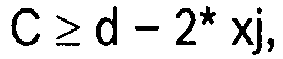
- the distance C which is defined essentially by the width of the insulating layer 10, is chosen so that the creepage distance of the solder to the PN junction 30 of both Lot 5 and Lot 4 is approximately identical. The following applies: C ⁇ d - 2 * xj
- Fig. 3 is the solder layer 5 in contact with the head wire 6, the solder layer 4 in contact with the base 1.
- the sides can also be reversed, so that the retracted solder layer 5 comes into contact with the base 1.
- the embodiment according to Fig. 3 includes a semiconductor chip whose PN junction 30 has a constant depth xj. Frequently, however, diode chips are also used in which the layers 3a and 3b have a different doping and a different penetration depth at the chip edge.
- the penetration depth xj at the chip edge is greater in a region A than in the inner region B of the chip.
- a narrow peripheral edge region A exhibits a higher breakdown voltage than the larger, internal region B.
- the penetration depth xj is now the depth of the PN junction 30 at the chip edge.
- completely different diodes can be located in areas A and B.
- a PN diode may be located in region A and a Schottky diode, trench barrier Schottky diode or the like in region B.
- Fig. 5 Another embodiment of the invention is therefore in Fig. 5 shown.
- Designations and layers are analogous to the first embodiment according to FIG Fig. 3 selected.
- the area of the insulating layer C is made larger than the width A. Basically, he can also be smaller than A.
- the width C again the relation designated by F1 from the first example applies. Again, the top and bottom of the chip can be reversed.
- Press-fit diodes according to the invention can be used in particular as rectifier diodes in AC generators, as a high-temperature resistant rectifier diodes in AC generators with recuperation or as particularly temperature-resistant bypass diodes in solar modules use.
Landscapes
- Rectifiers (AREA)
- Details Of Connecting Devices For Male And Female Coupling (AREA)
- Electrodes Of Semiconductors (AREA)
Description
- Die Erfindung betrifft eine Einpressdiode mit einer temperaturwechselfesten Lotverbindung. Eine derartige Diode eignet sich insbesondere als Diode für den Einsatz in Kfz-Generatorsystemen.
- In Kfz-Generatorsystemen werden zur Gleichrichtung des Wechsel- bzw. Drehstroms meist PN-Dioden aus Silizium eingesetzt. In der Regel werden diese Dioden in spezielle Gehäuse - sogenannte Einpressgehäuse - montiert, wie es aus der
Figur 1 ersichtlich ist. Die Einpressdioden weisen dabei einen mit einer Rändelung versehenen Einpresssockel 1 auf, der in eine entsprechende Aussparung einer Gleichrichteranordnung eingepresst ist. Der Einpresssockel übernimmt dabei gleichzeitig eine dauerhafte thermische und elektrische Verbindung der Gleichrichterdiode mit der Gleichrichteranordnung. Der Einpresssockel weist einen Befestigungsbereich auf, an dem ein Halbleiterchip 3 beispielsweise durch ein Lot 4 befestigt ist. Dabei ist die Ober- und Unterseite des Halbleiterchips 3 vollständig mit einer dünnen, in der Abbildung nicht eingezeichneten Metallisierung versehen. Die Metallisierung besteht beispielsweise aus einer Schichtenfolge von unterschiedlichen Metallen. Beispielsweise kann eine Schichtenfolge aus Cr, NiV7 und Ag Verwendung finden. Auf dem Halbleiterchip 3 wiederum ist ebenfalls beispielsweise durch ein Lot 5 ein sogenannter Kopfdraht 6 befestigt, der elektrisch durch Löten oder Schweißen oder einer sonstigen Befestigungstechnik fest mit anderen Komponenten des Gleichrichters kontaktiert ist. Der zwischen die beiden Kupferteile gelötete Siliziumchip 3 ist mit einer isolierenden Kunststoffmasse 7 umhüllt. Als Kunststoffmasse kann zum Beispiel ein mit Quarzkörnern gefülltes Epoxid oder ein sonstiger hoch temperaturfester Kunststoff dienen. Zur Einbringung der Kunststoffmasse 7 wird meist ein zusätzlicher Kunststoffring 8 angebracht. Oftmals befindet sich noch eine inFig. 1 nicht gezeichnete zusätzliche, weiche Kunststoffschicht zwischen dem Chip 3 und dem Epoxid 7. Die Kupferteile 4, 5 sind ggf. mit einer dünnen Oberflächenschicht aus Nickel versehen. - Bei einem Betrieb der Diode in Durchlassrichtung fällt an ihr eine Flussspannung UF ab, die sich bei Raumtemperatur und Stromdichten von 500A/cm2 etwa auf einen Wert von 1V einstellt. Der damit verbundene Leistungsabfall wird in Wärme umgewandelt und über das Einpressdiodengehäuse und den Gleichrichter des Generators abgeführt. Dadurch steigt die Sperrschichttemperatur Tj der Diode an. So werden bei hohen Generatorströmen und zusätzlich hohen Umgebungstemperaturen an der Diode Sperrschichttemperaturen Tj bis zu 240°C gemessen. In der Praxis werden die Dioden eines Kfz-Generators vielen Temperaturzyklen ausgesetzt. Beispielsweise sollen 3000 Temperaturzyklen mit einer Ausfallrate unter 1% überstanden werden. Verschärft wird die Situation durch vermehrten Einsatz von modernen Start-Stopp- bzw. Rekuperationssystemen, bei denen etwa 0,2- 2 Millionen Temperaturzyklen von etwa 40°C bis 80°C, die der mittleren Diodentemperatur überlagert sind, zusätzlich auftreten können.
- Bei den hohen Temperaturen darf das verwendete Lot 4,5 nicht aufschmelzen. Deshalb - sowie aus Gründen eines minimalen Lotverschleißes - wird ein Lot verwendet, dessen Schmelztemperatur Ts möglichst weit oberhalb der maximal auftretenden Sperrschichttemperatur Tj liegt. So werden bis heute in der Regel hoch bleihaltige Lote verwendet, deren Solidustemperatur Ts über 300°C liegt.
- Die in der Diode zusammengefügten Stoffe Silizium, bleihaltiges Lot und Kupfer weisen große Unterschiede in den physikalischen Materialeigenschaften auf. So sind beispielsweise Ausdehnungskoeffizienten und Elastizitätsmodule sehr unterschiedlich. Bei Temperaturwechseln treten deshalb hohe mechanische Spannungen auf. Die während den Temperaturhüben in den Bleiloten auftretende mechanische Spannung erreicht und übersteigt dabei schnell die Elastizitätsgrenze des Lots. Dies hat zur Folge, dass das Lot beginnt sich plastisch zu verformen. Dabei kommt es zu einem Vorgang, der als Lotkriechen bezeichnet wird. Im Fall der Einpressdiode quillt das Lot dabei im Laufe der Zeit aus seiner ursprünglichen Position heraus und kriecht entlang der Kupfer- bzw. Chipseiten weiter. Grundsätzlich tritt der beschriebene Effekt auch bei bleifreien Weichloten auf.
- In
Fig. 2 ist eine vergrößerte Darstellung eines Teils der in derFigur 1 gezeigten Einpressdiode im Querschnitt dargestellt. Die Bezeichnungen sind weitgehend mit denen inFig. 1 identisch. Der Halbleiterchip 3 ist in eine Zone 3a und eine Zone 3b mit unterschiedlichen Leitfähigkeitstypen, die durch einen PN-Übergang getrennt sind, aufgeteilt. Der PN-Übergang befindet sich in einer Eindringtiefe xj unterhalb der Chipoberseite. Die gesamte Chipdicke ist mit d bezeichnet. Die Zone 3a kann beispielsweise aus p-dotiertem und die Zone 3b aus n-dotiertem Silizium bestehen. Natürlich kann auch eine umgekehrte Schichtenfolge gewählt werden. Wesentlich ist, dass der PN-Übergang 30 bis zur Chipkante reicht, d. h. an der Chipkante austritt. - Tritt nun während des Betriebs mit Temperaturwechselbelastung Lotkriechen auf, kann das Lot entlang der Chipkanten kriechen. Insbesondere für den Fall, dass die Eindringtiefe xj klein ist, kann das Lot 5 leicht die Zone 3a überbrücken. Wenn das Lot 5 über die Zone 3a am Chiprand über den PN-Übergang 30 bis zum Bereich 3b wandert, ist die Diode kurzgeschlossen.
- Aus der
US 5,908,316 A und derEP 2 075 835 A2 sind bereits Dioden bekannt, die mit Kühl- und Kontaktierungskörpern verbunden sind. - Eine Einpressdiode mit den im Anspruch 1 angegebenen Merkmalen weist demgegenüber den Vorteil auf, dass der Kriechweg des Lotes verlängert ist und dadurch ein durch Lotkriechen hervorgerufener Kurzschluss hinausgezögert ist. Dadurch ist die Temperaturwechselfestigkeit einer Einpressdiode erhöht bzw. bei gleicher Temperaturwechselfestigkeit die maximal zulässige Chiptemperatur Tj erhöht. Ein weiterer Vorteil besteht darin, dass die Möglichkeit bereitgestellt wird, Halbleiterdioden mit sehr flachen PN-Übergängen in Einpressdiodengehäusen zu verpacken. Beispielsweise können statt der bisher üblichen Eindringtiefen von 30 µm - 60 µm auch Dioden mit Eindringtiefen im Bereich von 1µm oder darunter in Einpressdiodengehäusen montiert werden. Diese Vorteile werden dadurch erreicht, dass bei einer Einpressdiode, die einen durch Weichlot zwischen einem Sockel und einem Kopfdraht befestigten Halbleiterchip aufweist, bei dem mindestens ein PN-Übergang am Chipaußenrand endet, das Weichlot in dem Außenbereich, der den kleinsten Abstand vom PN-Übergang hat, relativ zum Chipaußenrand umlaufend zurückgezogen ist.
- Vorteilhafte Ausgestaltungen und Weiterbildungen der Erfindung sind in den abhängigen Ansprüchen angegeben.
- Nachfolgend wird die Erfindung anhand der
Figuren 3 - 5 beispielhaft erläutert. - Ein erstes Ausführungsbeispiel für eine Einpressdiode gemäß der Erfindung ist in der
Figur 3 veranschaulicht, in welcher eine vergrößerte Darstellung eines Teils einer Einpressdiode gemäß der Erfindung gezeigt ist. Im Gegensatz zu der bekannten Einpressdiode ist die Lotschicht 5, die sich in der Nähe des PN-Übergangs 30 befindet, um den Abstand C von der Chipkante zurückgezogen. Dies ist dadurch erreicht, dass sich zwischen Lot und Chipkante eine vollständig umlaufende, elektrisch isolierende dielektrische Schicht 10 befindet. Da das Weichlot 5 sich nur mit den Stellen des Chips verbindet, die aus der nicht eingezeichneten Chipmetallisierung bestehen, bildet sich eine Lotschicht auch nur an den Stellen aus, die nicht von der isolierenden Schicht 10 bedeckt sind. Die nicht eingezeichnete, lötfähige Chipmetallisierung besteht zum Beispiel aus einer dünnen Schichtenfolge von 70nm Cr, 300nm NiV7 und 250nm Ag. Natürlich können auch andere Schichtenfolgen Verwendung finden. Beispielsweise kann sich unter dem NiV eine dickere Aluminiumschicht befinden. Als isolierende Schichten können in der Halbleitertechnik übliche Materialien wie thermische Oxide, Low Temperature Oxides (LTO), dotierte Siliziumgläser wie BSPG, Siliziumnitridschichten usw., eingesetzt werden. Besonders vorteilhaft können auch Schichtenfolgen verwendet werden. So kann die Schicht beispielsweise aus 0,6 µm LTO + 1 µm Siliziumnitrid bestehen. - Der Abstand C, der im Wesentlichen durch die Breite der isolierenden Schicht 10 definiert ist, ist dabei so gewählt, dass der Kriechweg des Lotes bis zum PN-Übergang 30 sowohl von Lot 5 als auch von Lot 4 etwa identisch ist. Es gilt:

- In
Fig. 3 befindet sich die Lotschicht 5 in Kontakt mit dem Kopfdraht 6, die Lotschicht 4 in Kontakt mit dem Sockel 1. Selbstverständlich können die Seiten auch vertauscht werden, so dass die zurückgezogene Lotschicht 5 mit dem Sockel 1 in Berührung kommt. - Das Ausführungsbeispiel gemäß
Fig. 3 enthält einen Halbleiterchip, dessen PN-Übergang 30 eine konstante Tiefe xj aufweist. Häufig werden aber auch Diodenchips verwendet, bei denen die Schichten 3a und 3b am Chiprand eine andere Dotierung und eine andere Eindringtiefe aufweisen. - Dies ist in der
Fig. 4 veranschaulicht. Beispielsweise ist die Eindringtiefe xj am Chiprand in einem Bereich A größer als im inneren Bereich B des Chips. Dadurch kann beispielsweise erreicht werden, dass ein schmaler, umlaufender Randbereich A eine höhere Durchbruchsspannung als der größere, innere Bereich B zeigt. Als Eindringtiefe xj wird jetzt die Tiefe des PN-Übergangs 30 am Chiprand bezeichnet. Grundsätzlich können sich in den Bereichen A und B sogar vollständig unterschiedliche Dioden befinden. Beispielsweise kann sich im Bereich A eine PN-Diode und im Bereich B eine Schottkydiode, Trench-Barrrier-Schottkydiode oder ähnliches befinden. - Auch in diesem Fall besteht die Gefahr von Kurzschlüssen des PN-Überganges durch Lotkriechen. Ein weiteres erfindungsgemäßes Ausführungsbeispiel ist deshalb in
Fig. 5 dargestellt. Bezeichnungen und Schichten sind analog zum ersten Ausführungsbeispiel gemäßFig. 3 gewählt. InFig. 5 wird der Bereich der isolierenden Schicht C größer als die Weite A gewählt. Grundsätzlich kann er aber auch kleiner als A sein. Für die Auslegung der Weite C gilt wiederum die mit F1 bezeichnete Beziehung aus dem ersten Beispiel. Wiederum können Ober- und Unterseite des Chips vertauscht sein. - Einpressdioden gemäß der Erfindung können insbesondere als Gleichrichterdioden in Wechselstromgeneratoren, als besonders temperaturwechselfeste Gleichrichterdioden in Wechselstromgeneratoren mit Rekuperationsbetrieb oder als besonders temperaturwechselfeste Bypass-Dioden in Solarmodulen Verwendung finden.
Claims (8)
- Einpressdiode, die einen durch Weichlot zwischen einem Sockel und einem Kopfdraht befestigten Halbleiterchip aufweist, bei dem mindestens ein PN-Übergang am Chipaußenrand endet, dadurch gekennzeichnet, dass das Weichlot (5) auf einer ersten Seite in dem Außenbereich, der den kleinsten Abstand vom PN-Übergang (30) hat, relativ zum Chipaußenrand umlaufend zurückgezogen ist, indem sich über dem lotfreien Bereich des Halbleiterchips eine umlaufende, isolierende Schicht (10) befindet und dass eine zweite Seite des Halbleiterchips vollständig mit Weichlot (4) versehen ist.
- Einpressdiode nach Anspruch 1 oder 2, dadurch gekennzeichnet, dass die Eindringtiefe (xj) des PN-Überganges in einem Bereich (A) am Chiprand größer als die Eindringtiefe im Inneren des Halbleiterchips ist.
- Einpressdiode nach einem der vorhergehenden Ansprüche, dadurch gekennzeichnet, dass sich im Bereich (A) am Chiprand ein PN-Übergang mit der Eindringtiefe (xj) und im Inneren des Halbleiters eine Schottkydiode befindet.
- Einpressdiode nach einem der vorhergehenden Ansprüche, dadurch gekennzeichnet, dass sie als isolierende Schicht eine Kombination aus Oxiden und Siliziumnitrid aufweist.
- Einpressdiode nach einem der vorhergehenden Ansprüche, dadurch gekennzeichnet dass folgendes gilt:
- Einpressdiode nach einem der vorhergehenden Ansprüche, dadurch gekennzeichnet, dass als Halbleitermaterial ein Wide Band Gap Halbleiter verwendet wird, vorzugsweise SiC oder GaN.
- Einpressdiode nach einem der Ansprüche 3 - 5, dadurch gekennzeichnet, dass als Schottkydiode eine Trench-MOS-Barrier-Schottky-Diode (TMBS) verwendet ist.
- Einpressdiode nach einem der Ansprüche 3 - 5, dadurch gekennzeichnet, dass als Schottkydiode eine Trench-Junction-Barrier-Schottky-Diode (TJBS) verwendet ist.
Applications Claiming Priority (1)
| Application Number | Priority Date | Filing Date | Title |
|---|---|---|---|
| DE201010028196 DE102010028196A1 (de) | 2010-04-26 | 2010-04-26 | Temperaturwechselfeste Einpressdiode |
Publications (3)
| Publication Number | Publication Date |
|---|---|
| EP2381473A2 EP2381473A2 (de) | 2011-10-26 |
| EP2381473A3 EP2381473A3 (de) | 2016-05-25 |
| EP2381473B1 true EP2381473B1 (de) | 2018-10-03 |
Family
ID=43938463
Family Applications (1)
| Application Number | Title | Priority Date | Filing Date |
|---|---|---|---|
| EP11156124.7A Active EP2381473B1 (de) | 2010-04-26 | 2011-02-28 | Temperaturwechselfeste Einpressdiode |
Country Status (2)
| Country | Link |
|---|---|
| EP (1) | EP2381473B1 (de) |
| DE (1) | DE102010028196A1 (de) |
Families Citing this family (3)
| Publication number | Priority date | Publication date | Assignee | Title |
|---|---|---|---|---|
| EP2677540A1 (de) * | 2012-06-19 | 2013-12-25 | Nxp B.V. | Elektronische Vorrichtung und Verfahren zu dessen Herstellung |
| DE102012214056B4 (de) * | 2012-08-08 | 2020-10-29 | Robert Bosch Gmbh | Hoch temperaturwechselfeste Einpressdiode |
| CN108807428A (zh) * | 2018-04-26 | 2018-11-13 | 武汉高芯科技有限公司 | 带隔离栏的焦平面阵列及其制备方法 |
Family Cites Families (6)
| Publication number | Priority date | Publication date | Assignee | Title |
|---|---|---|---|---|
| US5908316A (en) * | 1995-12-18 | 1999-06-01 | Motorola, Inc. | Method of passivating a semiconductor substrate |
| US6362495B1 (en) * | 1998-03-05 | 2002-03-26 | Purdue Research Foundation | Dual-metal-trench silicon carbide Schottky pinch rectifier |
| JP4251326B2 (ja) * | 2004-03-30 | 2009-04-08 | サンケン電気株式会社 | 半導体装置 |
| EP1717863B1 (de) * | 2005-04-28 | 2011-11-02 | Ixys Corporation | Leistungshalbleiteranordnung mit Passivierungsschichten |
| US20070228505A1 (en) * | 2006-04-04 | 2007-10-04 | Mazzola Michael S | Junction barrier schottky rectifiers having epitaxially grown p+-n junctions and methods of making |
| DE102007063308A1 (de) * | 2007-12-28 | 2009-07-02 | Robert Bosch Gmbh | Diode |
-
2010
- 2010-04-26 DE DE201010028196 patent/DE102010028196A1/de not_active Withdrawn
-
2011
- 2011-02-28 EP EP11156124.7A patent/EP2381473B1/de active Active
Non-Patent Citations (1)
| Title |
|---|
| None * |
Also Published As
| Publication number | Publication date |
|---|---|
| DE102010028196A1 (de) | 2011-10-27 |
| EP2381473A2 (de) | 2011-10-26 |
| EP2381473A3 (de) | 2016-05-25 |
Similar Documents
| Publication | Publication Date | Title |
|---|---|---|
| DE112018005713B4 (de) | Leistungshalbleitereinheit und herstellungsverfahren für eine leistungshalbleitereinheit | |
| DE102014019973B4 (de) | Hochleistungs-Einzelchip-Halbleiter-Package und Verfahren zu dessen Fertigung und Halbleiterbaugruppe dies aufweisend | |
| WO2012107135A1 (de) | Trench-schottkydiode | |
| DE112013007447B4 (de) | Halbleitervorrichtung | |
| DE102016201071B4 (de) | Halbleitervorrichtung | |
| EP2757586B1 (de) | Leistungshalbleitermodul und Verfahren zur Herstellung eines Leistungshalbleitermoduls | |
| DE112014006908T5 (de) | Halbleitervorrichtung | |
| EP2462620B1 (de) | Halbleiteranordnung und verfahren zu deren herstellung | |
| DE102007063308A1 (de) | Diode | |
| EP1817799A1 (de) | Halbleitereinrichtung und gleichrichteranordnung | |
| EP3522233A1 (de) | Stapelförmige iii-v-halbleiterdiode | |
| DE102019213514B4 (de) | Halbleitervorrichtung und Verfahren zum Herstellen derselben | |
| DE102012112988A1 (de) | Optoelektronisches Bauelement, Verfahren zur Herstellung eines optoelektronischen Bauelements und Scheinwerfer | |
| EP2381473A2 (de) | Temperaturwechselfeste Einpressdiode | |
| DE102017200252A1 (de) | Halbleitervorrichtung | |
| EP2499669B1 (de) | Schutzelement für elektronische schaltungen | |
| DE112013007220T5 (de) | Halbleitervorrichtung | |
| EP3955288A1 (de) | Leistungsmodul mit einer verbindungsschicht aufweisend eine lotschicht und einen abstandshalter, elektrisches gerät mit dem leistungsmodul und verfahren zur herstellung des leistungsmoduls | |
| WO2011057848A1 (de) | Schottkydiode | |
| DE102012214056B4 (de) | Hoch temperaturwechselfeste Einpressdiode | |
| DE102024110706A1 (de) | Elektrisches verbindungselement mit ausgasungskerben | |
| DE102010028199A1 (de) | Einpressdiode | |
| DE102011088418B4 (de) | Bondverbindung | |
| EP1203410B1 (de) | Halbleitererzeugnis mit einem schottky-kontakt | |
| DE102021207739A1 (de) | Verfahren zum verpacken einer gleichrichteranordnung und eine gleichrichteranordnung |
Legal Events
| Date | Code | Title | Description |
|---|---|---|---|
| AK | Designated contracting states |
Kind code of ref document: A2 Designated state(s): AL AT BE BG CH CY CZ DE DK EE ES FI FR GB GR HR HU IE IS IT LI LT LU LV MC MK MT NL NO PL PT RO RS SE SI SK SM TR |
|
| AX | Request for extension of the european patent |
Extension state: BA ME |
|
| PUAI | Public reference made under article 153(3) epc to a published international application that has entered the european phase |
Free format text: ORIGINAL CODE: 0009012 |
|
| PUAL | Search report despatched |
Free format text: ORIGINAL CODE: 0009013 |
|
| AK | Designated contracting states |
Kind code of ref document: A3 Designated state(s): AL AT BE BG CH CY CZ DE DK EE ES FI FR GB GR HR HU IE IS IT LI LT LU LV MC MK MT NL NO PL PT RO RS SE SI SK SM TR |
|
| AX | Request for extension of the european patent |
Extension state: BA ME |
|
| RIC1 | Information provided on ipc code assigned before grant |
Ipc: H01L 29/06 20060101ALI20160419BHEP Ipc: H01L 23/051 20060101AFI20160419BHEP Ipc: H01L 29/861 20060101ALI20160419BHEP |
|
| STAA | Information on the status of an ep patent application or granted ep patent |
Free format text: STATUS: REQUEST FOR EXAMINATION WAS MADE |
|
| 17P | Request for examination filed |
Effective date: 20161125 |
|
| RBV | Designated contracting states (corrected) |
Designated state(s): AL AT BE BG CH CY CZ DE DK EE ES FI FR GB GR HR HU IE IS IT LI LT LU LV MC MK MT NL NO PL PT RO RS SE SI SK SM TR |
|
| RAP1 | Party data changed (applicant data changed or rights of an application transferred) |
Owner name: SEG AUTOMOTIVE GERMANY GMBH |
|
| RAP1 | Party data changed (applicant data changed or rights of an application transferred) |
Owner name: SEG AUTOMOTIVE GERMANY GMBH Owner name: ROBERT BOSCH GMBH |
|
| GRAP | Despatch of communication of intention to grant a patent |
Free format text: ORIGINAL CODE: EPIDOSNIGR1 |
|
| STAA | Information on the status of an ep patent application or granted ep patent |
Free format text: STATUS: GRANT OF PATENT IS INTENDED |
|
| RIC1 | Information provided on ipc code assigned before grant |
Ipc: H01L 29/20 20060101ALN20180530BHEP Ipc: H01L 29/16 20060101ALN20180530BHEP Ipc: H01L 23/051 20060101AFI20180530BHEP Ipc: H01L 29/861 20060101ALI20180530BHEP Ipc: H01L 29/06 20060101ALI20180530BHEP |
|
| RIC1 | Information provided on ipc code assigned before grant |
Ipc: H01L 29/16 20060101ALN20180605BHEP Ipc: H01L 29/06 20060101ALI20180605BHEP Ipc: H01L 29/20 20060101ALN20180605BHEP Ipc: H01L 23/051 20060101AFI20180605BHEP Ipc: H01L 29/861 20060101ALI20180605BHEP |
|
| INTG | Intention to grant announced |
Effective date: 20180621 |
|
| RIC1 | Information provided on ipc code assigned before grant |
Ipc: H01L 29/16 20060101ALN20180608BHEP Ipc: H01L 29/06 20060101ALI20180608BHEP Ipc: H01L 23/051 20060101AFI20180608BHEP Ipc: H01L 29/861 20060101ALI20180608BHEP Ipc: H01L 29/20 20060101ALN20180608BHEP |
|
| GRAS | Grant fee paid |
Free format text: ORIGINAL CODE: EPIDOSNIGR3 |
|
| GRAA | (expected) grant |
Free format text: ORIGINAL CODE: 0009210 |
|
| STAA | Information on the status of an ep patent application or granted ep patent |
Free format text: STATUS: THE PATENT HAS BEEN GRANTED |
|
| AK | Designated contracting states |
Kind code of ref document: B1 Designated state(s): AL AT BE BG CH CY CZ DE DK EE ES FI FR GB GR HR HU IE IS IT LI LT LU LV MC MK MT NL NO PL PT RO RS SE SI SK SM TR |
|
| REG | Reference to a national code |
Ref country code: GB Ref legal event code: FG4D Free format text: NOT ENGLISH |
|
| REG | Reference to a national code |
Ref country code: CH Ref legal event code: EP Ref country code: AT Ref legal event code: REF Ref document number: 1049548 Country of ref document: AT Kind code of ref document: T Effective date: 20181015 |
|
| REG | Reference to a national code |
Ref country code: DE Ref legal event code: R096 Ref document number: 502011014784 Country of ref document: DE |
|
| REG | Reference to a national code |
Ref country code: IE Ref legal event code: FG4D Free format text: LANGUAGE OF EP DOCUMENT: GERMAN |
|
| REG | Reference to a national code |
Ref country code: NL Ref legal event code: MP Effective date: 20181003 |
|
| REG | Reference to a national code |
Ref country code: LT Ref legal event code: MG4D |
|
| PG25 | Lapsed in a contracting state [announced via postgrant information from national office to epo] |
Ref country code: NL Free format text: LAPSE BECAUSE OF FAILURE TO SUBMIT A TRANSLATION OF THE DESCRIPTION OR TO PAY THE FEE WITHIN THE PRESCRIBED TIME-LIMIT Effective date: 20181003 |
|
| PG25 | Lapsed in a contracting state [announced via postgrant information from national office to epo] |
Ref country code: FI Free format text: LAPSE BECAUSE OF FAILURE TO SUBMIT A TRANSLATION OF THE DESCRIPTION OR TO PAY THE FEE WITHIN THE PRESCRIBED TIME-LIMIT Effective date: 20181003 Ref country code: IS Free format text: LAPSE BECAUSE OF FAILURE TO SUBMIT A TRANSLATION OF THE DESCRIPTION OR TO PAY THE FEE WITHIN THE PRESCRIBED TIME-LIMIT Effective date: 20190203 Ref country code: CZ Free format text: LAPSE BECAUSE OF FAILURE TO SUBMIT A TRANSLATION OF THE DESCRIPTION OR TO PAY THE FEE WITHIN THE PRESCRIBED TIME-LIMIT Effective date: 20181003 Ref country code: NO Free format text: LAPSE BECAUSE OF FAILURE TO SUBMIT A TRANSLATION OF THE DESCRIPTION OR TO PAY THE FEE WITHIN THE PRESCRIBED TIME-LIMIT Effective date: 20190103 Ref country code: LV Free format text: LAPSE BECAUSE OF FAILURE TO SUBMIT A TRANSLATION OF THE DESCRIPTION OR TO PAY THE FEE WITHIN THE PRESCRIBED TIME-LIMIT Effective date: 20181003 Ref country code: ES Free format text: LAPSE BECAUSE OF FAILURE TO SUBMIT A TRANSLATION OF THE DESCRIPTION OR TO PAY THE FEE WITHIN THE PRESCRIBED TIME-LIMIT Effective date: 20181003 Ref country code: BG Free format text: LAPSE BECAUSE OF FAILURE TO SUBMIT A TRANSLATION OF THE DESCRIPTION OR TO PAY THE FEE WITHIN THE PRESCRIBED TIME-LIMIT Effective date: 20190103 Ref country code: LT Free format text: LAPSE BECAUSE OF FAILURE TO SUBMIT A TRANSLATION OF THE DESCRIPTION OR TO PAY THE FEE WITHIN THE PRESCRIBED TIME-LIMIT Effective date: 20181003 Ref country code: HR Free format text: LAPSE BECAUSE OF FAILURE TO SUBMIT A TRANSLATION OF THE DESCRIPTION OR TO PAY THE FEE WITHIN THE PRESCRIBED TIME-LIMIT Effective date: 20181003 Ref country code: PL Free format text: LAPSE BECAUSE OF FAILURE TO SUBMIT A TRANSLATION OF THE DESCRIPTION OR TO PAY THE FEE WITHIN THE PRESCRIBED TIME-LIMIT Effective date: 20181003 |
|
| PG25 | Lapsed in a contracting state [announced via postgrant information from national office to epo] |
Ref country code: AL Free format text: LAPSE BECAUSE OF FAILURE TO SUBMIT A TRANSLATION OF THE DESCRIPTION OR TO PAY THE FEE WITHIN THE PRESCRIBED TIME-LIMIT Effective date: 20181003 Ref country code: PT Free format text: LAPSE BECAUSE OF FAILURE TO SUBMIT A TRANSLATION OF THE DESCRIPTION OR TO PAY THE FEE WITHIN THE PRESCRIBED TIME-LIMIT Effective date: 20190203 Ref country code: SE Free format text: LAPSE BECAUSE OF FAILURE TO SUBMIT A TRANSLATION OF THE DESCRIPTION OR TO PAY THE FEE WITHIN THE PRESCRIBED TIME-LIMIT Effective date: 20181003 Ref country code: GR Free format text: LAPSE BECAUSE OF FAILURE TO SUBMIT A TRANSLATION OF THE DESCRIPTION OR TO PAY THE FEE WITHIN THE PRESCRIBED TIME-LIMIT Effective date: 20190104 Ref country code: RS Free format text: LAPSE BECAUSE OF FAILURE TO SUBMIT A TRANSLATION OF THE DESCRIPTION OR TO PAY THE FEE WITHIN THE PRESCRIBED TIME-LIMIT Effective date: 20181003 |
|
| REG | Reference to a national code |
Ref country code: DE Ref legal event code: R097 Ref document number: 502011014784 Country of ref document: DE |
|
| PG25 | Lapsed in a contracting state [announced via postgrant information from national office to epo] |
Ref country code: DK Free format text: LAPSE BECAUSE OF FAILURE TO SUBMIT A TRANSLATION OF THE DESCRIPTION OR TO PAY THE FEE WITHIN THE PRESCRIBED TIME-LIMIT Effective date: 20181003 |
|
| PLBE | No opposition filed within time limit |
Free format text: ORIGINAL CODE: 0009261 |
|
| STAA | Information on the status of an ep patent application or granted ep patent |
Free format text: STATUS: NO OPPOSITION FILED WITHIN TIME LIMIT |
|
| PG25 | Lapsed in a contracting state [announced via postgrant information from national office to epo] |
Ref country code: SM Free format text: LAPSE BECAUSE OF FAILURE TO SUBMIT A TRANSLATION OF THE DESCRIPTION OR TO PAY THE FEE WITHIN THE PRESCRIBED TIME-LIMIT Effective date: 20181003 Ref country code: EE Free format text: LAPSE BECAUSE OF FAILURE TO SUBMIT A TRANSLATION OF THE DESCRIPTION OR TO PAY THE FEE WITHIN THE PRESCRIBED TIME-LIMIT Effective date: 20181003 Ref country code: RO Free format text: LAPSE BECAUSE OF FAILURE TO SUBMIT A TRANSLATION OF THE DESCRIPTION OR TO PAY THE FEE WITHIN THE PRESCRIBED TIME-LIMIT Effective date: 20181003 Ref country code: SK Free format text: LAPSE BECAUSE OF FAILURE TO SUBMIT A TRANSLATION OF THE DESCRIPTION OR TO PAY THE FEE WITHIN THE PRESCRIBED TIME-LIMIT Effective date: 20181003 |
|
| 26N | No opposition filed |
Effective date: 20190704 |
|
| REG | Reference to a national code |
Ref country code: CH Ref legal event code: PL |
|
| GBPC | Gb: european patent ceased through non-payment of renewal fee |
Effective date: 20190228 |
|
| PG25 | Lapsed in a contracting state [announced via postgrant information from national office to epo] |
Ref country code: LU Free format text: LAPSE BECAUSE OF NON-PAYMENT OF DUE FEES Effective date: 20190228 Ref country code: MC Free format text: LAPSE BECAUSE OF FAILURE TO SUBMIT A TRANSLATION OF THE DESCRIPTION OR TO PAY THE FEE WITHIN THE PRESCRIBED TIME-LIMIT Effective date: 20181003 Ref country code: SI Free format text: LAPSE BECAUSE OF FAILURE TO SUBMIT A TRANSLATION OF THE DESCRIPTION OR TO PAY THE FEE WITHIN THE PRESCRIBED TIME-LIMIT Effective date: 20181003 |
|
| REG | Reference to a national code |
Ref country code: BE Ref legal event code: MM Effective date: 20190228 |
|
| REG | Reference to a national code |
Ref country code: IE Ref legal event code: MM4A |
|
| PG25 | Lapsed in a contracting state [announced via postgrant information from national office to epo] |
Ref country code: LI Free format text: LAPSE BECAUSE OF NON-PAYMENT OF DUE FEES Effective date: 20190228 Ref country code: CH Free format text: LAPSE BECAUSE OF NON-PAYMENT OF DUE FEES Effective date: 20190228 |
|
| PG25 | Lapsed in a contracting state [announced via postgrant information from national office to epo] |
Ref country code: IE Free format text: LAPSE BECAUSE OF NON-PAYMENT OF DUE FEES Effective date: 20190228 Ref country code: GB Free format text: LAPSE BECAUSE OF NON-PAYMENT OF DUE FEES Effective date: 20190228 |
|
| PG25 | Lapsed in a contracting state [announced via postgrant information from national office to epo] |
Ref country code: BE Free format text: LAPSE BECAUSE OF NON-PAYMENT OF DUE FEES Effective date: 20190228 |
|
| PG25 | Lapsed in a contracting state [announced via postgrant information from national office to epo] |
Ref country code: TR Free format text: LAPSE BECAUSE OF FAILURE TO SUBMIT A TRANSLATION OF THE DESCRIPTION OR TO PAY THE FEE WITHIN THE PRESCRIBED TIME-LIMIT Effective date: 20181003 |
|
| REG | Reference to a national code |
Ref country code: AT Ref legal event code: MM01 Ref document number: 1049548 Country of ref document: AT Kind code of ref document: T Effective date: 20190228 |
|
| PG25 | Lapsed in a contracting state [announced via postgrant information from national office to epo] |
Ref country code: AT Free format text: LAPSE BECAUSE OF NON-PAYMENT OF DUE FEES Effective date: 20190228 |
|
| PG25 | Lapsed in a contracting state [announced via postgrant information from national office to epo] |
Ref country code: MT Free format text: LAPSE BECAUSE OF FAILURE TO SUBMIT A TRANSLATION OF THE DESCRIPTION OR TO PAY THE FEE WITHIN THE PRESCRIBED TIME-LIMIT Effective date: 20181003 |
|
| PGFP | Annual fee paid to national office [announced via postgrant information from national office to epo] |
Ref country code: IT Payment date: 20210226 Year of fee payment: 11 |
|
| PG25 | Lapsed in a contracting state [announced via postgrant information from national office to epo] |
Ref country code: CY Free format text: LAPSE BECAUSE OF FAILURE TO SUBMIT A TRANSLATION OF THE DESCRIPTION OR TO PAY THE FEE WITHIN THE PRESCRIBED TIME-LIMIT Effective date: 20181003 |
|
| PG25 | Lapsed in a contracting state [announced via postgrant information from national office to epo] |
Ref country code: HU Free format text: LAPSE BECAUSE OF FAILURE TO SUBMIT A TRANSLATION OF THE DESCRIPTION OR TO PAY THE FEE WITHIN THE PRESCRIBED TIME-LIMIT; INVALID AB INITIO Effective date: 20110228 |
|
| PG25 | Lapsed in a contracting state [announced via postgrant information from national office to epo] |
Ref country code: MK Free format text: LAPSE BECAUSE OF FAILURE TO SUBMIT A TRANSLATION OF THE DESCRIPTION OR TO PAY THE FEE WITHIN THE PRESCRIBED TIME-LIMIT Effective date: 20181003 |
|
| PG25 | Lapsed in a contracting state [announced via postgrant information from national office to epo] |
Ref country code: IT Free format text: LAPSE BECAUSE OF NON-PAYMENT OF DUE FEES Effective date: 20220228 |
|
| PGFP | Annual fee paid to national office [announced via postgrant information from national office to epo] |
Ref country code: DE Payment date: 20250422 Year of fee payment: 15 |
|
| REG | Reference to a national code |
Ref country code: DE Ref legal event code: R079 Ref document number: 502011014784 Country of ref document: DE Free format text: PREVIOUS MAIN CLASS: H01L0023051000 Ipc: H10W0076138000 |
|
| PGFP | Annual fee paid to national office [announced via postgrant information from national office to epo] |
Ref country code: FR Payment date: 20260223 Year of fee payment: 16 |