EP2378666B1 - Digital controller for automatic rate detection and tracking of audio interface clocks - Google Patents
Digital controller for automatic rate detection and tracking of audio interface clocks Download PDFInfo
- Publication number
- EP2378666B1 EP2378666B1 EP10392003.9A EP10392003A EP2378666B1 EP 2378666 B1 EP2378666 B1 EP 2378666B1 EP 10392003 A EP10392003 A EP 10392003A EP 2378666 B1 EP2378666 B1 EP 2378666B1
- Authority
- EP
- European Patent Office
- Prior art keywords
- clock
- fractional
- digital
- register
- phase error
- Prior art date
- Legal status (The legal status is an assumption and is not a legal conclusion. Google has not performed a legal analysis and makes no representation as to the accuracy of the status listed.)
- Active
Links
Images


Classifications
-
- H—ELECTRICITY
- H03—ELECTRONIC CIRCUITRY
- H03L—AUTOMATIC CONTROL, STARTING, SYNCHRONISATION OR STABILISATION OF GENERATORS OF ELECTRONIC OSCILLATIONS OR PULSES
- H03L7/00—Automatic control of frequency or phase; Synchronisation
- H03L7/06—Automatic control of frequency or phase; Synchronisation using a reference signal applied to a frequency- or phase-locked loop
- H03L7/07—Automatic control of frequency or phase; Synchronisation using a reference signal applied to a frequency- or phase-locked loop using several loops, e.g. for redundant clock signal generation
-
- H—ELECTRICITY
- H03—ELECTRONIC CIRCUITRY
- H03L—AUTOMATIC CONTROL, STARTING, SYNCHRONISATION OR STABILISATION OF GENERATORS OF ELECTRONIC OSCILLATIONS OR PULSES
- H03L7/00—Automatic control of frequency or phase; Synchronisation
- H03L7/06—Automatic control of frequency or phase; Synchronisation using a reference signal applied to a frequency- or phase-locked loop
- H03L7/16—Indirect frequency synthesis, i.e. generating a desired one of a number of predetermined frequencies using a frequency- or phase-locked loop
- H03L7/18—Indirect frequency synthesis, i.e. generating a desired one of a number of predetermined frequencies using a frequency- or phase-locked loop using a frequency divider or counter in the loop
- H03L7/197—Indirect frequency synthesis, i.e. generating a desired one of a number of predetermined frequencies using a frequency- or phase-locked loop using a frequency divider or counter in the loop a time difference being used for locking the loop, the counter counting between numbers which are variable in time or the frequency divider dividing by a factor variable in time, e.g. for obtaining fractional frequency division
- H03L7/1974—Indirect frequency synthesis, i.e. generating a desired one of a number of predetermined frequencies using a frequency- or phase-locked loop using a frequency divider or counter in the loop a time difference being used for locking the loop, the counter counting between numbers which are variable in time or the frequency divider dividing by a factor variable in time, e.g. for obtaining fractional frequency division for fractional frequency division
- H03L7/1976—Indirect frequency synthesis, i.e. generating a desired one of a number of predetermined frequencies using a frequency- or phase-locked loop using a frequency divider or counter in the loop a time difference being used for locking the loop, the counter counting between numbers which are variable in time or the frequency divider dividing by a factor variable in time, e.g. for obtaining fractional frequency division for fractional frequency division using a phase accumulator for controlling the counter or frequency divider
-
- H—ELECTRICITY
- H03—ELECTRONIC CIRCUITRY
- H03L—AUTOMATIC CONTROL, STARTING, SYNCHRONISATION OR STABILISATION OF GENERATORS OF ELECTRONIC OSCILLATIONS OR PULSES
- H03L7/00—Automatic control of frequency or phase; Synchronisation
- H03L7/06—Automatic control of frequency or phase; Synchronisation using a reference signal applied to a frequency- or phase-locked loop
- H03L7/16—Indirect frequency synthesis, i.e. generating a desired one of a number of predetermined frequencies using a frequency- or phase-locked loop
- H03L7/22—Indirect frequency synthesis, i.e. generating a desired one of a number of predetermined frequencies using a frequency- or phase-locked loop using more than one loop
- H03L7/23—Indirect frequency synthesis, i.e. generating a desired one of a number of predetermined frequencies using a frequency- or phase-locked loop using more than one loop with pulse counters or frequency dividers
- H03L7/235—Nested phase locked loops
-
- H—ELECTRICITY
- H03—ELECTRONIC CIRCUITRY
- H03L—AUTOMATIC CONTROL, STARTING, SYNCHRONISATION OR STABILISATION OF GENERATORS OF ELECTRONIC OSCILLATIONS OR PULSES
- H03L7/00—Automatic control of frequency or phase; Synchronisation
- H03L7/06—Automatic control of frequency or phase; Synchronisation using a reference signal applied to a frequency- or phase-locked loop
- H03L7/08—Details of the phase-locked loop
- H03L7/085—Details of the phase-locked loop concerning mainly the frequency- or phase-detection arrangement including the filtering or amplification of its output signal
- H03L7/095—Details of the phase-locked loop concerning mainly the frequency- or phase-detection arrangement including the filtering or amplification of its output signal using a lock detector
Definitions
- This invention relates generally to digital audio COder-DECoders (CODECs) and relates more specifically to synchronization of a master clock with digital audio signals coming from separate clock domains.
- Digital audio CODECs typically use a stable master clock as a reference and a phase-locked loop (PLL) to generate the frequencies required for processing the audio data.
- PLL phase-locked loop
- these devices may also be required to maintain synchronization with digital audio signals coming from a separate clock domain, These signals will not be synchronous to the master clock and they may also drift with respect to the master clock.
- the signal frequencies may also change depending on the source.
- the slave device must therefore be capable of tracking a range of incoming data streams so that audio signal samples are not lost.
- U. S. Patent Publication proposes an apparatus and method for compensating for a phase jump of a reference signal in a digital Phase-Locked Loop (PLL)/Frequency-Locked Loop (FLL).
- the apparatus includes a phase discriminator for comparing a phase of an external clock signal (i.e., the reference signal) with a phase of an internal clock signal to determine a phase difference between the two signals, a phase jump compensator, and for correcting the phase difference by using a phase jump correction value obtained in the estimation process, and a Low Pass Filter (LPF) for filtering a high-frequency component of the corrected phase difference.
- PLL Phase-Locked Loop
- FLL Frequency-Locked Loop
- U. S. Patent discloses a method and system for synchronizing video information derived from an asynchronously sampled video signal providing a mechanism for using asynchronous sampling in the front-end of digital video capture systems.
- a ratio between the sampling clock frequency and the source video clock frequency is computed via an all digital phase-lock loop (ADPLL) and either a video clock is generated from the ratio by another PLL, a number to clock converter or the ratio is used directly to provide digital synchronization information to downstream processing blocks.
- a sample rate converter SRC
- SRC sample rate converter
- U. S. Patent ( US 5,790,615 to Beale et al. ) describes a digital phase-lock loop network that provides input and output clock signals to a digital data receiving system generally, and particularly to a data buffer contained therein.
- the digital phase-lock loop network provides bit-clock synchronization using a fixed input clock and an output clock having a variable frequency that is adjusted to correspond to the average input rate of the data samples into the data buffer.
- the digital phase-lock loop network allows the data buffer to be operated as a temporary storage device maintaining a nominal number of data samples therein at all times by avoiding any overflow and underflow data handling conditions that may otherwise cause loss of data.
- the digital phase-lock loop network of the present invention is particularly suited for the Eureka-147 system, which has become a worldwide standard for digital audio broadcasting (DAB) technology.
- DAB digital audio broadcasting
- U. S. Patent Publication ( US 2008/0075152 to Melanson ) teaches a hybrid analog/digital phase-lock loop with high-level event synchronization providing a mechanism for generating a low-jitter clock from a timing reference that has a high jitter level and synchronizing the output clock to high-level events.
- a numerically-controlled analog oscillator provides a clock output and a counter divides the frequency of the clock output to provide input to a digital phase-frequency detector for detecting an on-going phase-frequency difference between the timing reference and the output of the counter.
- a synchronization circuit detects or receives a high-level event signal, and resets the on-going phase-frequency difference and optionally the counter to synchronize the clock output with the events.
- US2006/166627 discloses a circuit for data synchronization In devices which transmit and/or receive audio and/or video data through the staged locking of phase locked loops.
- US6201486 B1 discloses a pre-processing of the multiple sources of digital input data to be converted to analog by Digital to Analog Converters (DAC), such that differences in Input sampling rates can be accommodated.
- DAC Digital to Analog Converters
- a principal object of the present invention is to achieve systems and methods capable to automatically detecting a change in data-rate, selecting the correct gearing ratio, and re-establishing synchronization with the new audio source,
- a further object of the invention is to remove the need for a handover procedure when switching between audio sources
- a further object of the invention is to enabling a system to switch between audio data sources of unknown rates.
- a further object of the invention is to achieve a system for the automatic rate detection and tracking of digital data streams.
- a further object of the invention is to achieve a system, which applies in particular to a digital audio interface that operates at a number of well-defined and well-spaced rates, but could be applied to other similar systems.
- a further object of the invention is to remove the need to know or communicate in advance the rate at which the interface will be operating, so allowing asynchronous switching between different audio data streams.
- an object of the invention is to track deviations and drift between actual and ideal rate of date streams.
- a digital audio interface uses a protocol known as lnter-lC Sound (l2S, which consists of (at a minimum)) two clock signals and a data signal.
- the first clock (“bit” clock) is used as a sampling clock for the data signal.
- the second clock (“word” clock) or “LR” clock) is used to define the word boundaries and can also be used to split the data between left and right audio channels. All that is significant here is that the l2S word clock runs at the sample rate of the audio data, e. g. for 44.1 kilo samples per second (ksps) CD audio data the l2S word clock runs at 44.1 kHz.
- the l2S word clock is simply referred to as the l2S clock in the remainder of the description.
- the present invention comprises a digital controller that works with a phase-lock loop (PLL).
- PLL phase-lock loop
- the PLL is a fractional-N loop, used to derive the device clock from the master clock.
- the digital controller itself acts as a phase-lock loop by modifying the feedback divide ratio of the PLL in order to minimize the phase error between the device clock and an arbitrary audio interface clock.
- Fig. 1 illustrates an overall block diagram of a digital l2S tracking controller and analog phase-lock loop.
- the PLL comprises a phase frequency detector / charge pump unit (PFD / CP) 1 , a loop filter 2 , a voltage controlled oscillator (VCO) 3, a feedback divider 4 , a Sigma-Delta Modulator 5 , a Lock-Detect Unit 6 , and the l2S tracking controller 7 .
- the PLL clock frequency 12 is part of the inputs to the l2S tracking controller 7 .
- the PLL is a fractional-N loop and the frequency of the VCO 3 is reduced by a division by a factor N in a first frequency reduction block 8 .
- a second frequency reduction block 9 the frequency of the VCO 3 , which has already reduced been in block 8 , is further been reduced by factor M to accommodate to the frequency required by the device clock.
- Other values of N and M could be chosen for this and other systems.
- the VCO clock 3 When the system is in lock, the VCO clock 3 is phase locked to the master clock 10 and is also phase-locked to the l2S clock 11 . ln order to keep the overall system stable, the l2S tracking controller 7 operates with a much lower bandwidth than the analog PLL.
- Fig. 2 shows an internal block diagram of the l2S tracking controller 7 .
- the clock from the analog PLL is divided by a prescaler 20 , to reduce the high frequency PLL signal 12 to a lower frequency by integer division, and used to increment the COUNTER register 21 by 1.
- the l2S clock 11 is used to transfer the COUNTER 21 contents to the CAPTURE 22 block and to increment the COMPARE register 23 by 256 (0 ⁇ 100).
- COMPARE register 23 is subtracted from CAPTURE 22 by unit 24 to calculate the phase error ( PE ) 27 , and this together with its derivative PE' 26 , gained from block PREVIOUS PE 25 , is fed into the CONTROL block 28 .
- the CONTROL block 28 computes the offset "deltax", as shown in Fig.
- phase error When the system has achieved synchronization with the l2S clock 11 , the phase error will be zero, which implies that there are exactly 256 (prescaled) PLL clock 12 cycles per l2S clock 11 cycles.
- the Controller 28 could also be designed alternatively for other numbers of PLL clock cycles per l2S clock cycles, e.g., 128, 512, or others.
- a PLL clock cycle per l2S clock cycles of 256 is a preferred number of cycles as a good compromise between frequency resolution and power consumption.
- the automatic detection of the 12S rate exploits the fact that there are only a limited number of valid l2S rates, e.g.8 kHz, 44.1 kHz, etc.
- the DIFFERENCE register 28 records by how much the CAPTURE register 22 has changed.
- the DIFFERENCE register 28 should always contain the value 256. lf this value does not equal 256, it can indicate that the incoming l2S rate has changed and, together with the current l2S rate, it can be used to compute the new l2S rate.
- the DIFFERENCE register 28 values used to automatically detect and decode an l2S rate change are shown in the table of Fig. 3 .
- the PLL clock prescaler 20 can be updated according to the table of Fig. 4 , showing PLL clock prescaler values for 12S rate settings.
- the l2S tracking controller 7 is unable to distinguish between (for example) 44.1 kHz and 48.0 kHz, and it uses the same internal settings for both.
- the analog PLL should lock to one VCO 3 frequency for all 48.0 kHz rates (8.0, 12.0, 16.0, 24.0, 32.0, 48.0 and 96.0 kHz) and another VCO frequency for all 44.1 kHz rates (11.025, 22.05, 44.1 and 88.2 kHz).
- the nominal divide ratio see Fig.
- the sign of the "deltax" correction applied by the l2S tracking controller 7 to the sigma-delta modulator 7 can be used to distinguish between the two groups of rates. This allows the controller to completely determine the incoming l2S rate, and this information can be used by the rest of the system to select appropriate settings.
- the digital controller can not only distinguish between 44.1 kHz and 48,0 kHz as shown above but also for other different l2S rates, having the same internal settings, such as 11.025 kHz and 12.0 kHz, or 22.05kHz and 24.0 kHz, etc as shown in the table of Fig. 3 . ln summary, the correct group of l2S rates is determined by the digital controller by setting a nominal divide ratio such that a nominal frequency of a VCO of the first PLL is set mid-way between an upper and a lower end of a determined l2S rate group, having both common internal settings, and a sign of a correction applied to the first PLL is used to distinguish between both groups of rates.
- the PLL only ever locks the VCO to one of two frequencies, one for the 44.1 kHz group of rates (11.025, 22.05, 44.1, 88.2kHz) and one for the 48kHz group of rates (8, 12, 16, 24, 32, 48, 96kHz). So the nominal mid-way divide ratio is the same for all I2S rates - it is only determined by the master clock frequency 10.
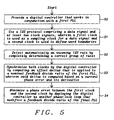
- Fig. 5 illustrates a flowchart of a method invented for a digital audio interface, which doesn't require a handover procedure when switching between audio sources and allowing to switch between audio data sources of unknown rates.
- a first step 50 describes the provision of a digital controller that works in conjunction with a first phase-lock loop.
- a next step 51 illustrates using an I2S protocol comprising a data signal and at least two clock signals, wherein a first clock is used as a sampling clock for a data signal and a second clock is used to define word boundaries.
- Step 52 describes detecting automatically an incoming I2S rate by completely determining a correct group of rates.
- Step 53 teaches synchronizing both clocks by the digital controller by computing an offset deltax that is applied to a nominal feedback divide ratio of the first PLL, wherein said deltax is computed based on a current phase error and its derivative.
- Step 54 discloses minimizing a phase error between the first clock and the second clock by deploying the digital controller as another phase-lock loop that modifies a feedback divide ratio of the first PLL.
Landscapes
- Stabilization Of Oscillater, Synchronisation, Frequency Synthesizers (AREA)
- Synchronisation In Digital Transmission Systems (AREA)
Description
- This invention relates generally to digital audio COder-DECoders (CODECs) and relates more specifically to synchronization of a master clock with digital audio signals coming from separate clock domains.
- Digital audio CODECs typically use a stable master clock as a reference and a phase-locked loop (PLL) to generate the frequencies required for processing the audio data. When used in slave mode, these devices may also be required to maintain synchronization with digital audio signals coming from a separate clock domain, These signals will not be synchronous to the master clock and they may also drift with respect to the master clock. In a complex system with a multiplicity of data sources, the signal frequencies may also change depending on the source. The slave device must therefore be capable of tracking a range of incoming data streams so that audio signal samples are not lost.
- Current systems require knowledge of the incoming audio data rate so that an appropriate "gearing ratio" can be selected. This requires some form of handover protocol when switching between audio sources and precludes either switching between audio sources on the fly or switching to an unknown audio source.
- It is a challenge for the designers of CODECs to achieve systems capable to automatically detecting a change in data-rate, selecting the correct gearing ratio, and re-establishing synchronization with the new audio source,
- There are known patents or patent publications dealing with synchronization with digital audio/video sources.
- U. S. Patent Publication (
US 2008/0198958 to Shin ) proposes an apparatus and method for compensating for a phase jump of a reference signal in a digital Phase-Locked Loop (PLL)/Frequency-Locked Loop (FLL). The apparatus includes a phase discriminator for comparing a phase of an external clock signal (i.e., the reference signal) with a phase of an internal clock signal to determine a phase difference between the two signals, a phase jump compensator, and for correcting the phase difference by using a phase jump correction value obtained in the estimation process, and a Low Pass Filter (LPF) for filtering a high-frequency component of the corrected phase difference. - U. S. Patent (
US 7,499,106 to Gudmunson et al. ) discloses a method and system for synchronizing video information derived from an asynchronously sampled video signal providing a mechanism for using asynchronous sampling in the front-end of digital video capture systems. A ratio between the sampling clock frequency and the source video clock frequency is computed via an all digital phase-lock loop (ADPLL) and either a video clock is generated from the ratio by another PLL, a number to clock converter or the ratio is used directly to provide digital synchronization information to downstream processing blocks. A sample rate converter (SRC) is provided in an interpolator that either acts as a sample position corrector at the same line rate as the received video, or by introducing an offset in the ADPLL, the video data can be converted to another line rate via the SRC. - U. S. Patent (
US 5,790,615 to Beale et al. ) describes a digital phase-lock loop network that provides input and output clock signals to a digital data receiving system generally, and particularly to a data buffer contained therein. The digital phase-lock loop network provides bit-clock synchronization using a fixed input clock and an output clock having a variable frequency that is adjusted to correspond to the average input rate of the data samples into the data buffer. The digital phase-lock loop network allows the data buffer to be operated as a temporary storage device maintaining a nominal number of data samples therein at all times by avoiding any overflow and underflow data handling conditions that may otherwise cause loss of data. The digital phase-lock loop network of the present invention is particularly suited for the Eureka-147 system, which has become a worldwide standard for digital audio broadcasting (DAB) technology. - Furthermore U. S. Patent Publication (
US 2008/0075152 to Melanson ) teaches a hybrid analog/digital phase-lock loop with high-level event synchronization providing a mechanism for generating a low-jitter clock from a timing reference that has a high jitter level and synchronizing the output clock to high-level events. A numerically-controlled analog oscillator provides a clock output and a counter divides the frequency of the clock output to provide input to a digital phase-frequency detector for detecting an on-going phase-frequency difference between the timing reference and the output of the counter. A synchronization circuit detects or receives a high-level event signal, and resets the on-going phase-frequency difference and optionally the counter to synchronize the clock output with the events. -
US2006/166627 discloses a circuit for data synchronization In devices which transmit and/or receive audio and/or video data through the staged locking of phase locked loops. -
US6201486 B1 discloses a pre-processing of the multiple sources of digital input data to be converted to analog by Digital to Analog Converters (DAC), such that differences in Input sampling rates can be accommodated. - A principal object of the present invention is to achieve systems and methods capable to automatically detecting a change in data-rate, selecting the correct gearing ratio, and re-establishing synchronization with the new audio source,
- A further object of the invention is to remove the need for a handover procedure when switching between audio sources
- A further object of the invention is to enabling a system to switch between audio data sources of unknown rates.
- A further object of the invention is to achieve a system for the automatic rate detection and tracking of digital data streams.
- A further object of the invention is to achieve a system, which applies in particular to a digital audio interface that operates at a number of well-defined and well-spaced rates, but could be applied to other similar systems.
- A further object of the invention is to remove the need to know or communicate in advance the rate at which the interface will be operating, so allowing asynchronous switching between different audio data streams.
- Moreover an object of the invention is to track deviations and drift between actual and ideal rate of date streams.
- In accordance with the objects of this invention a method for a digital audio interface, which doesn't require a handover procedure when switching between audio sources and allowing to switch between audio data sources of unknown rates, has been achieved by the features of the appended claims.
- ln accordance with the objects of this invention a digital audio interface, using an 12S protocol, without the need for a handover procedure when switching between audio sources, has been achieved by the features of the appended claims.
- In the accompanying drawings forming a material part of this description, there is shown:
-
Fig. 1 illustrates an overall block diagram of a digital l2S tracking controller and analog phase-lock loop. -
Fig. 2 shows an internal block diagram of the l2S tracking controller -
Fig. 3 shows in a table DIFFERENCE register values used to automatically detect and decode an l2S rate change. -
Fig. 4 illustrates in a table PLL clock prescaler values for l2S settings. -
Fig. 5 illustrates a flowchart of a method invented for a digital audio interface, which doesn't require a handover procedure when switching between audio sources and allowing to switch between audio data sources of unknown rates. - Systems and methods for a digital controller for automatic rate detection and tracking of audio interface clocks are disclosed.
- A digital audio interface uses a protocol known as lnter-lC Sound (l2S, which consists of (at a minimum)) two clock signals and a data signal. The first clock ("bit" clock) is used as a sampling clock for the data signal. The second clock ("word" clock) or "LR" clock) is used to define the word boundaries and can also be used to split the data between left and right audio channels. All that is significant here is that the l2S word clock runs at the sample rate of the audio data, e. g. for 44.1 kilo samples per second (ksps) CD audio data the l2S word clock runs at 44.1 kHz. The l2S word clock is simply referred to as the l2S clock in the remainder of the description.
- The present invention comprises a digital controller that works with a phase-lock loop (PLL). The PLL is a fractional-N loop, used to derive the device clock from the master clock. The digital controller itself acts as a phase-lock loop by modifying the feedback divide ratio of the PLL in order to minimize the phase error between the device clock and an arbitrary audio interface clock.
-
Fig. 1 illustrates an overall block diagram of a digital l2S tracking controller and analog phase-lock loop. The PLL comprises a phase frequency detector / charge pump unit (PFD / CP) 1, aloop filter 2, a voltage controlled oscillator (VCO) 3, afeedback divider 4, a Sigma-DeltaModulator 5, a Lock-Detect Unit 6, and thel2S tracking controller 7. ThePLL clock frequency 12 is part of the inputs to thel2S tracking controller 7. - The PLL is a fractional-N loop and the frequency of the
VCO 3 is reduced by a division by a factor N in a firstfrequency reduction block 8. ln a secondfrequency reduction block 9 the frequency of theVCO 3, which has already reduced been inblock 8, is further been reduced by factor M to accommodate to the frequency required by the device clock. In the preferred embodiment N = 4 and M = 8 since the l2S tracking controller requires a faster clock than the device clock. Other values of N and M could be chosen for this and other systems. - When the system is in lock, the
VCO clock 3 is phase locked to themaster clock 10 and is also phase-locked to thel2S clock 11. ln order to keep the overall system stable, thel2S tracking controller 7 operates with a much lower bandwidth than the analog PLL. -
Fig. 2 shows an internal block diagram of thel2S tracking controller 7. The clock from the analog PLL is divided by aprescaler 20, to reduce the highfrequency PLL signal 12 to a lower frequency by integer division, and used to increment theCOUNTER register 21 by 1.Thel2S clock 11 is used to transfer theCOUNTER 21 contents to theCAPTURE 22 block and to increment theCOMPARE register 23 by 256 (0×100).COMPARE register 23 is subtracted fromCAPTURE 22 byunit 24 to calculate the phase error (PE) 27, and this together with its derivative PE' 26, gained from block PREVIOUSPE 25, is fed into theCONTROL block 28. Once every update cycle, theCONTROL block 28 computes the offset "deltax", as shown inFig. 1 the X+ΔX input to the Sigma-Delta Modulator 5, that should be applied to the nominal feedback divide ratio of the analog PLL. When thel2S tracking controller 7 is locked, the update cycle runs at approximately 10Hz to avoid producing audible artifacts. - When the system has achieved synchronization with the
l2S clock 11, the phase error will be zero, which implies that there are exactly 256 (prescaled)PLL clock 12 cycles perl2S clock 11 cycles. TheController 28 could also be designed alternatively for other numbers of PLL clock cycles per l2S clock cycles, e.g., 128, 512, or others. A PLL clock cycle per l2S clock cycles of 256 is a preferred number of cycles as a good compromise between frequency resolution and power consumption. - The automatic detection of the 12S rate exploits the fact that there are only a limited number of valid l2S rates, e.g.8 kHz, 44.1 kHz, etc. On each l2S cycle the DIFFERENCE register 28 records by how much the
CAPTURE register 22 has changed. When the system is in synchronization theDIFFERENCE register 28 should always contain the value 256. lf this value does not equal 256, it can indicate that the incoming l2S rate has changed and, together with the current l2S rate, it can be used to compute the new l2S rate. - The DIFFERENCE register 28 values used to automatically detect and decode an l2S rate change are shown in the table of
Fig. 3 . Once the new l2S rate has been decoded, thePLL clock prescaler 20 can be updated according to the table ofFig. 4 , showing PLL clock prescaler values for 12S rate settings. - As the table of
Fig. 3 shows, thel2S tracking controller 7 is unable to distinguish between (for example) 44.1 kHz and 48.0 kHz, and it uses the same internal settings for both. However the analog PLL should lock to oneVCO 3 frequency for all 48.0 kHz rates (8.0, 12.0, 16.0, 24.0, 32.0, 48.0 and 96.0 kHz) and another VCO frequency for all 44.1 kHz rates (11.025, 22.05, 44.1 and 88.2 kHz). By setting the nominal divide ratio (seeFig. 1 ) such that the nominal VCO frequency is mid-way between the 48.0 kHz and 44.1 kHz settings, the sign of the "deltax" correction applied by thel2S tracking controller 7 to the sigma-delta modulator 7 can be used to distinguish between the two groups of rates. This allows the controller to completely determine the incoming l2S rate, and this information can be used by the rest of the system to select appropriate settings. - It is obvious that the digital controller can not only distinguish between 44.1 kHz and 48,0 kHz as shown above but also for other different l2S rates, having the same internal settings, such as 11.025 kHz and 12.0 kHz, or 22.05kHz and 24.0 kHz, etc as shown in the table of
Fig. 3 . ln summary, the correct group of l2S rates is determined by the digital controller by setting a nominal divide ratio such that a nominal frequency of a VCO of the first PLL is set mid-way between an upper and a lower end of a determined l2S rate group, having both common internal settings, and a sign of a correction applied to the first PLL is used to distinguish between both groups of rates. The PLL only ever locks the VCO to one of two frequencies, one for the 44.1 kHz group of rates (11.025, 22.05, 44.1, 88.2kHz) and one for the 48kHz group of rates (8, 12, 16, 24, 32, 48, 96kHz). So the nominal mid-way divide ratio is the same for all I2S rates - it is only determined by themaster clock frequency 10. -
Fig. 5 illustrates a flowchart of a method invented for a digital audio interface, which doesn't require a handover procedure when switching between audio sources and allowing to switch between audio data sources of unknown rates. Afirst step 50 describes the provision of a digital controller that works in conjunction with a first phase-lock loop. Anext step 51 illustrates using an I2S protocol comprising a data signal and at least two clock signals, wherein a first clock is used as a sampling clock for a data signal and a second clock is used to define word boundaries.Step 52 describes detecting automatically an incoming I2S rate by completely determining a correct group of rates.Step 53 teaches synchronizing both clocks by the digital controller by computing an offset deltax that is applied to a nominal feedback divide ratio of the first PLL, wherein said deltax is computed based on a current phase error and its derivative.Step 54 discloses minimizing a phase error between the first clock and the second clock by deploying the digital controller as another phase-lock loop that modifies a feedback divide ratio of the first PLL.
Claims (13)
- A method for a digital audio interface, allowing switching between audio data sources of unknown rates, comprising the following steps:(1) providing a digital tracking controller (7) that works in conjunction with a first fractional-N-loop PLL (1-6) which receives a master clock (10) and outputs a device clock (12);characterized in that it further comprises the steps of:(2) using an I2S protocol comprising a data signal and an I2S word clock (11) used to define word boundaries in said data signal;(3) detecting automatically an incoming I2S rate by determining a correct I2S rate group wherein an I2S rate group comprises those I2S rates which the digital audio interface can process correctly for a given set of settings - for example, frequency division ratios - within said digital audio interface, wherein said determined I2S rate group is determined by the digital tracking controller (7) by setting a nominal feedback divide ratio in the first fractional-N loop PLL (1-6) such that a nominal frequency of a VCO (3) of the first fractional-N-loop PLL (1-6) is set mid-way between an upper and a lower end of the determined I2S rate group, and a sign of an offset deltax signal applied to the first fractional-N-loop PLL (1-6) is used to distinguish between whether the incoming I2S rate is closest to the upper end or the lower end of the determined I2S rate group;(4) synchronizing the master dock (10) with the I2S word clock (11) by the digital tracking controller (7) by computing the offset deltax signal that is applied to the nominal feedback divide ratio of the first fractional-N-loop PLL, wherein said offset deltax signal is computed based on a current phase error between the master clock (10) and the I2S word clock (11) and the derivative of said current phase error; andwherein said synchronizing is achieved by minimizing the phase error between the master clock (10) and the IS2 word dock (11) by deploying the digital tracking controller (7) as another phase-lock loop that modifies the nominal feedback divide ratio of the first fractional-N-loop PLL (1-6).
- The method of claim 1 wherein said digital tracking controller (7) operates with a much lower bandwidth than the first fractional-N n-loop PLL (1-6), wherein the operating frequency of the digital tracking controller is set by integer division.
- The method of claim 1 wherein the synchronization by said digital tracking controller (7) comprises steps of:(4a) dividing a clock of the first fractional-N-loop PLL (1-6) by a prescaler (20) and using the result to increment a counter register (21) by 1;(4b) transferring the content of the counter register (21) to a capture register (22) and incrementing a compare register (23) by a defined number using the IS2 word clock (11);(4c) calculating the phase error between the master clock (10) and the 12S word clock (11) by subtracting the compare register (23) from the capture register (22) and feeding the phase error together with the derivative of said phase error into a control block (28); and(4d) computing said offset deltax signal by the control block (28) and applying said offset deltax signal to said nominal feedback divide ratio of the first PLL (1-6).
- The method of claim 3 wherein the control block (28) computes said offset deltax signal correspondent to an update cycle wherein the update cycle comprises the step of calculating the phase error between the I2S word clock (11) and the master clock (10), the step of feeding the phase error together with its derivative into the control block (28), the step of computing said offset deltax signal, the step of applying the offset deltax signal to said nominal feedback divide ratio of the first fractional-N-loop PLL, and repeating the update cycle until the phase error between the master clock and the I2S word (11) is zero..
- The method of claim 4 wherein said update cycle runs at approximately 10Hz when the voltage-controlled oscillator (3) is phase-locked to the master clock (10) and is also phase-locked to the I2S word clock (11).
- The method of claim 3 wherein said defined number is 256.
- A digital audio interface, using an I2S protocol comprising a data signal and an I2S word clock (11) allowing switching between audio data sources of unknown rates when switching between audio sources,
characterized in that it comprises:- a first fractional-N loop PLL (1-6), configured to derive a device clock (12) from a master clock (10), and- a digital tracking controller (7), acting itself as another phase-lock loop by modifying a nominal feedback divide ratio between the master clock (10) and the device clock (12) generated by the fractional-N loop PLL (1-6) in order to minimize a phase error between the device clock (12) and the I2S word dock (11), having Inputs and an output, wherein a first input is the nominal feedback divide ratio, a second Input is the I2S word clock (11), a third input is a lock detect signal from the fractional-N loop PLL (1-6), and a fourth input is the device clock (12) from the fractional-N loop PLL, and the output is an offset deltax signal applied to the nominal feedback divide ratio of the fractional-N loop PLL in order to achieve a lock between the device clock (12) and the I2S word clock (11); whereinthe offset deltax signal is computed based on a current phase error between the master clock (10) and the I2S word clock (11) and the derivative of said current phase error; and
the digital tracking controller (7) detects automatically an incoming I2S rate group, wherein an I2S rate group comprise those I2S rates which the digital audio interface can process correctly for a given set of settings - for example, frequency division ratios-within said digital audio interface, by setting the nominal feedback divide ratio such that a nominal frequency of a VCO (3) of the first fractional-N loop PLL is set mid-way between an upper and a lower end of the incoming I2S rate group. - The digital audio interface of claim 7, wherein said fractional-N loop PLL (1-6) comprises:- a phase frequency detector and charge pump unit (1) having inputs and an output, wherein a first input receives signals from the master clock, a second input is the output of a feedback divider block (4), and the output is input to a loop filter (2);- said loop fllter (2), wherein Its output is the input of a voltage controlled oscillator (3);- said voltage controlled oscillator (3), wherein its output is input to a frequency reduction block (8), to a lock detect block (6), and to a feedback divider block (4) having said nominal feedback divide ratio, wherein the system is in lock when the voltage controlled oscillator (3) is phase locked to the master clock (10) and is also phase-locked to the I2S word clock (11) and in this state a signal is sent to a lock detecting block (6) to Indicate a lock status; wherein- said feedback divider block (4) receives an input from a sigma-delta modulator (5);- said frequency reduction block (8) reduces the frequency of the signal received from the voltage-controlled oscillator by a factor N;- said Lock Detect block (6) detectes a lock of the device clock (12) to the I2S word clock (11); and- said sigma-delta modulator (5) receives inputs from said feedback divider block (4) and said digital tracking controller (7) and provides an output to said feedback divider block (4).
- The digital audio Interface of claim 8, wherein said digital tracking controller (7) comprises:- a means to prescale (20) clock signals received from said fractional-N loop PLL (1-6), wherein an output of the means to prescale (20) is connected to a means to count (21);- said means to count (21), having its output connected to a capture register (22);- said capture register (22), having its output connected to a difference register (28);- said difference register (28), which is used to decode an I2S rate change, having its output connected to an I2S_rate register;- said I2S_rate register, whose output updates a prescale factor of said means to prescale (20) dock signals, and having a clock input which is also connected to a control block (28) and to a phase error register (25, 26);- a compare register (23), which upon being clocked by said I2S word clock (11) is incremented by a digital value and whose content is subtracted from said capture register (22) to calculate the phase error between the device clock (12) and the 12S word clock (11), which is stored In the phase error register (25, 26) and a input directly to said control block (28);- said phase error register (25, 26), which calculates a derivative of a current phase error between the device clock (12) and the I2S word clock (11) and provides the derivative to said control block (28);- said control block (28), providing said offset deltax signal applied to the nominal feedback divide ratio of the fractional-N loop PLL (1-6).
- The digital audio Interface of claim 7, wherein said digital controller (7) operates with a much lower bandwidth than the fractional-N loop PLL.
- The digital audio interface of claim 7, wherein a clock signal received (8) from said fractional-N loop PLL is frequency divided by said means to prescale (20) clock signals and used to increment said means to count (21) by one.
- The digital audio interface of claim 7, wherein the I2S word clock (11) is used to transfer the content of said means to count (21) to said capture register (22) and to Increment said compare register (23) by a digital value.
- The digital audio interface of claim 12, wherein said digital value corresponds to 256.
Applications Claiming Priority (2)
| Application Number | Priority Date | Filing Date | Title |
|---|---|---|---|
| US27864509P | 2009-10-08 | 2009-10-08 | |
| US12/592,598 US8433027B2 (en) | 2009-10-08 | 2009-11-30 | Digital controller for automatic rate detection and tracking of audio interface clocks |
Publications (3)
| Publication Number | Publication Date |
|---|---|
| EP2378666A2 EP2378666A2 (en) | 2011-10-19 |
| EP2378666A3 EP2378666A3 (en) | 2012-05-30 |
| EP2378666B1 true EP2378666B1 (en) | 2013-09-25 |
Family
ID=43855474
Family Applications (1)
| Application Number | Title | Priority Date | Filing Date |
|---|---|---|---|
| EP10392003.9A Active EP2378666B1 (en) | 2009-10-08 | 2010-10-07 | Digital controller for automatic rate detection and tracking of audio interface clocks |
Country Status (2)
| Country | Link |
|---|---|
| US (1) | US8433027B2 (en) |
| EP (1) | EP2378666B1 (en) |
Families Citing this family (15)
| Publication number | Priority date | Publication date | Assignee | Title |
|---|---|---|---|---|
| EP2771973B1 (en) | 2011-10-25 | 2017-08-30 | Cirrus Logic International Semiconductor Ltd. | Asynchronous sample rate converter |
| GB2496673B (en) * | 2011-11-21 | 2014-06-11 | Wolfson Microelectronics Plc | Clock generator |
| US9281827B2 (en) | 2011-11-21 | 2016-03-08 | Cirrus Logic International Semiconductor Ltd. | Clock generator |
| CN108880750B (en) * | 2012-07-09 | 2021-07-06 | 索尼公司 | Decoding and demodulation apparatus and method, receiving apparatus and method, and communication system |
| US9906396B2 (en) | 2013-04-30 | 2018-02-27 | Sony Corporation | Coding and modulation apparatus using non-uniform constellation |
| US20160156498A1 (en) | 2013-07-05 | 2016-06-02 | Sony Corporation | Coding and modulation apparatus using non-uniform constellation |
| US9584139B2 (en) * | 2014-09-24 | 2017-02-28 | Intel IP Corporation | Phase tracker for a phase locked loop |
| CN108604979B (en) * | 2016-02-02 | 2021-05-18 | 马维尔亚洲私人有限公司 | Method and apparatus for network synchronization |
| DE102016007576B3 (en) * | 2016-06-21 | 2017-11-02 | Audi Ag | Transmission of TDM-coded data over a communication channel according to the I²S protocol |
| US20190005974A1 (en) * | 2017-06-28 | 2019-01-03 | Qualcomm Incorporated | Alignment of bi-directional multi-stream multi-rate i2s audio transmitted between integrated circuits |
| CN112306932B (en) * | 2020-11-27 | 2023-12-01 | 珠海一微半导体股份有限公司 | An interface protocol multiplexing method and chip |
| US11558170B2 (en) * | 2020-12-16 | 2023-01-17 | Synaptics Incorporated | Phase-locked loop with dual input reference and dynamic bandwidth control |
| CN114165298B (en) * | 2021-11-25 | 2024-01-09 | 盛子测控科技(沈阳市)有限责任公司 | Method and device for realizing phase-locked tracking and positioning of rotor blade by frequency multiplication and frequency division |
| CN115426564B (en) * | 2022-08-23 | 2025-07-01 | 昆山海菲曼科技集团股份有限公司 | A headphone audio amplifier for eliminating phase noise |
| TWI873541B (en) * | 2023-02-15 | 2025-02-21 | 瑞昱半導體股份有限公司 | Audio restore circuit |
Family Cites Families (8)
| Publication number | Priority date | Publication date | Assignee | Title |
|---|---|---|---|---|
| US5703539A (en) * | 1993-12-17 | 1997-12-30 | Motorola, Inc. | Apparatus and method for controlling the loop bandwidth of a phase locked loop |
| US5790615A (en) * | 1995-12-11 | 1998-08-04 | Delco Electronics Corporation | Digital phase-lock loop network |
| JP3824737B2 (en) * | 1997-05-20 | 2006-09-20 | 富士通株式会社 | Servo signal processing device |
| US6201486B1 (en) * | 1999-12-01 | 2001-03-13 | Creative Technology Ltd. | Pre-processing of multiple sample rates sources to simplify and improve multi-channel DAC design |
| US7474724B1 (en) * | 2004-10-13 | 2009-01-06 | Cirrus Logic, Inc. | Method and system for video-synchronous audio clock generation from an asynchronously sampled video signal |
| US7443213B2 (en) * | 2005-01-21 | 2008-10-28 | Thomson Licensing | Staged locking of two phase locked loops |
| US7599462B2 (en) * | 2006-09-25 | 2009-10-06 | Cirrus Logic, Inc. | Hybrid analog/digital phase-lock loop with high-level event synchronization |
| KR101055679B1 (en) * | 2007-02-16 | 2011-08-09 | 삼성전자주식회사 | Apparatus and method for synchronous phase jump compensation in a digital phase tracking loop or a frequency tracking loop |
-
2009
- 2009-11-30 US US12/592,598 patent/US8433027B2/en active Active
-
2010
- 2010-10-07 EP EP10392003.9A patent/EP2378666B1/en active Active
Also Published As
| Publication number | Publication date |
|---|---|
| US8433027B2 (en) | 2013-04-30 |
| EP2378666A2 (en) | 2011-10-19 |
| EP2378666A3 (en) | 2012-05-30 |
| US20110087347A1 (en) | 2011-04-14 |
Similar Documents
| Publication | Publication Date | Title |
|---|---|---|
| US8433027B2 (en) | Digital controller for automatic rate detection and tracking of audio interface clocks | |
| EP1129580B1 (en) | Clock recovery | |
| US8428045B2 (en) | Media clock recovery | |
| US6326851B1 (en) | Digital phase-domain PLL frequency synthesizer | |
| US7746972B1 (en) | Numerically-controlled phase-lock loop with input timing reference-dependent ratio adjustment | |
| US6052034A (en) | Method and apparatus for all digital holdover circuit | |
| WO2013126440A2 (en) | Automatic detection and compensation of frequency offset in point-to-point communication | |
| JP2002076886A (en) | Digital fractional phase detector | |
| US7558358B1 (en) | Method and apparatus for generating a clock signal according to an ideal frequency ratio | |
| CN101321294A (en) | Sound clock regenerator with accurate tracking mechanism | |
| WO2001011781A1 (en) | Clock synchronization system and method | |
| US7599462B2 (en) | Hybrid analog/digital phase-lock loop with high-level event synchronization | |
| JP2006217203A (en) | Digital pll circuit | |
| US11575498B2 (en) | Clock and data recovery circuits | |
| US20100246736A1 (en) | Clock recovery from data streams containing embedded reference clock values | |
| WO2018090037A1 (en) | Systems and methods for phase synchronization of local oscillator paths in oscillator-operated circuits | |
| EP2153523B1 (en) | Frequency synchronization | |
| CN101542959B (en) | Method, circuit and system for receiving data | |
| JP2518148B2 (en) | Clock dependent synchronization method | |
| CN103329440B (en) | Phase-frequency detection method | |
| US7158045B1 (en) | Method and apparatus for maintaining an ideal frequency ratio between numerically-controlled frequency sources | |
| WO2005086759A2 (en) | Method and apparatus for crystal drift compensation | |
| JP3542978B2 (en) | Frequency synchronization device and frequency synchronization control method | |
| JP3886392B2 (en) | Clock recovery circuit | |
| JP4651348B2 (en) | Digital audio adjustment device |
Legal Events
| Date | Code | Title | Description |
|---|---|---|---|
| AK | Designated contracting states |
Kind code of ref document: A2 Designated state(s): AL AT BE BG CH CY CZ DE DK EE ES FI FR GB GR HR HU IE IS IT LI LT LU LV MC MK MT NL NO PL PT RO RS SE SI SK SM TR |
|
| AX | Request for extension of the european patent |
Extension state: BA ME |
|
| PUAI | Public reference made under article 153(3) epc to a published international application that has entered the european phase |
Free format text: ORIGINAL CODE: 0009012 |
|
| PUAL | Search report despatched |
Free format text: ORIGINAL CODE: 0009013 |
|
| AK | Designated contracting states |
Kind code of ref document: A3 Designated state(s): AL AT BE BG CH CY CZ DE DK EE ES FI FR GB GR HR HU IE IS IT LI LT LU LV MC MK MT NL NO PL PT RO RS SE SI SK SM TR |
|
| AX | Request for extension of the european patent |
Extension state: BA ME |
|
| RIC1 | Information provided on ipc code assigned before grant |
Ipc: H03L 7/197 20060101ALI20120425BHEP Ipc: H03L 7/23 20060101AFI20120425BHEP Ipc: H03L 7/07 20060101ALI20120425BHEP Ipc: H03L 7/095 20060101ALN20120425BHEP |
|
| 17P | Request for examination filed |
Effective date: 20121127 |
|
| GRAP | Despatch of communication of intention to grant a patent |
Free format text: ORIGINAL CODE: EPIDOSNIGR1 |
|
| INTG | Intention to grant announced |
Effective date: 20130408 |
|
| RIC1 | Information provided on ipc code assigned before grant |
Ipc: H03L 7/197 20060101ALI20130325BHEP Ipc: H03L 7/095 20060101ALN20130325BHEP Ipc: H03L 7/23 20060101AFI20130325BHEP Ipc: H03L 7/07 20060101ALI20130325BHEP |
|
| GRAS | Grant fee paid |
Free format text: ORIGINAL CODE: EPIDOSNIGR3 |
|
| GRAA | (expected) grant |
Free format text: ORIGINAL CODE: 0009210 |
|
| AK | Designated contracting states |
Kind code of ref document: B1 Designated state(s): AL AT BE BG CH CY CZ DE DK EE ES FI FR GB GR HR HU IE IS IT LI LT LU LV MC MK MT NL NO PL PT RO RS SE SI SK SM TR |
|
| REG | Reference to a national code |
Ref country code: GB Ref legal event code: FG4D |
|
| REG | Reference to a national code |
Ref country code: CH Ref legal event code: EP |
|
| REG | Reference to a national code |
Ref country code: AT Ref legal event code: REF Ref document number: 634047 Country of ref document: AT Kind code of ref document: T Effective date: 20131015 |
|
| REG | Reference to a national code |
Ref country code: IE Ref legal event code: FG4D |
|
| REG | Reference to a national code |
Ref country code: DE Ref legal event code: R096 Ref document number: 602010010518 Country of ref document: DE Effective date: 20131121 |
|
| PG25 | Lapsed in a contracting state [announced via postgrant information from national office to epo] |
Ref country code: SE Free format text: LAPSE BECAUSE OF FAILURE TO SUBMIT A TRANSLATION OF THE DESCRIPTION OR TO PAY THE FEE WITHIN THE PRESCRIBED TIME-LIMIT Effective date: 20130925 Ref country code: HR Free format text: LAPSE BECAUSE OF FAILURE TO SUBMIT A TRANSLATION OF THE DESCRIPTION OR TO PAY THE FEE WITHIN THE PRESCRIBED TIME-LIMIT Effective date: 20130925 Ref country code: NO Free format text: LAPSE BECAUSE OF FAILURE TO SUBMIT A TRANSLATION OF THE DESCRIPTION OR TO PAY THE FEE WITHIN THE PRESCRIBED TIME-LIMIT Effective date: 20131225 Ref country code: LT Free format text: LAPSE BECAUSE OF FAILURE TO SUBMIT A TRANSLATION OF THE DESCRIPTION OR TO PAY THE FEE WITHIN THE PRESCRIBED TIME-LIMIT Effective date: 20130925 |
|
| REG | Reference to a national code |
Ref country code: AT Ref legal event code: MK05 Ref document number: 634047 Country of ref document: AT Kind code of ref document: T Effective date: 20130925 |
|
| REG | Reference to a national code |
Ref country code: NL Ref legal event code: VDEP Effective date: 20130925 |
|
| REG | Reference to a national code |
Ref country code: LT Ref legal event code: MG4D |
|
| PG25 | Lapsed in a contracting state [announced via postgrant information from national office to epo] |
Ref country code: LV Free format text: LAPSE BECAUSE OF FAILURE TO SUBMIT A TRANSLATION OF THE DESCRIPTION OR TO PAY THE FEE WITHIN THE PRESCRIBED TIME-LIMIT Effective date: 20130925 Ref country code: SI Free format text: LAPSE BECAUSE OF FAILURE TO SUBMIT A TRANSLATION OF THE DESCRIPTION OR TO PAY THE FEE WITHIN THE PRESCRIBED TIME-LIMIT Effective date: 20130925 Ref country code: RS Free format text: LAPSE BECAUSE OF FAILURE TO SUBMIT A TRANSLATION OF THE DESCRIPTION OR TO PAY THE FEE WITHIN THE PRESCRIBED TIME-LIMIT Effective date: 20130925 Ref country code: FI Free format text: LAPSE BECAUSE OF FAILURE TO SUBMIT A TRANSLATION OF THE DESCRIPTION OR TO PAY THE FEE WITHIN THE PRESCRIBED TIME-LIMIT Effective date: 20130925 Ref country code: GR Free format text: LAPSE BECAUSE OF FAILURE TO SUBMIT A TRANSLATION OF THE DESCRIPTION OR TO PAY THE FEE WITHIN THE PRESCRIBED TIME-LIMIT Effective date: 20131226 |
|
| PG25 | Lapsed in a contracting state [announced via postgrant information from national office to epo] |
Ref country code: BE Free format text: LAPSE BECAUSE OF FAILURE TO SUBMIT A TRANSLATION OF THE DESCRIPTION OR TO PAY THE FEE WITHIN THE PRESCRIBED TIME-LIMIT Effective date: 20130925 |
|
| PG25 | Lapsed in a contracting state [announced via postgrant information from national office to epo] |
Ref country code: NL Free format text: LAPSE BECAUSE OF FAILURE TO SUBMIT A TRANSLATION OF THE DESCRIPTION OR TO PAY THE FEE WITHIN THE PRESCRIBED TIME-LIMIT Effective date: 20130925 Ref country code: SK Free format text: LAPSE BECAUSE OF FAILURE TO SUBMIT A TRANSLATION OF THE DESCRIPTION OR TO PAY THE FEE WITHIN THE PRESCRIBED TIME-LIMIT Effective date: 20130925 Ref country code: EE Free format text: LAPSE BECAUSE OF FAILURE TO SUBMIT A TRANSLATION OF THE DESCRIPTION OR TO PAY THE FEE WITHIN THE PRESCRIBED TIME-LIMIT Effective date: 20130925 Ref country code: IS Free format text: LAPSE BECAUSE OF FAILURE TO SUBMIT A TRANSLATION OF THE DESCRIPTION OR TO PAY THE FEE WITHIN THE PRESCRIBED TIME-LIMIT Effective date: 20140125 Ref country code: CZ Free format text: LAPSE BECAUSE OF FAILURE TO SUBMIT A TRANSLATION OF THE DESCRIPTION OR TO PAY THE FEE WITHIN THE PRESCRIBED TIME-LIMIT Effective date: 20130925 Ref country code: RO Free format text: LAPSE BECAUSE OF FAILURE TO SUBMIT A TRANSLATION OF THE DESCRIPTION OR TO PAY THE FEE WITHIN THE PRESCRIBED TIME-LIMIT Effective date: 20130925 |
|
| PG25 | Lapsed in a contracting state [announced via postgrant information from national office to epo] |
Ref country code: CY Free format text: LAPSE BECAUSE OF FAILURE TO SUBMIT A TRANSLATION OF THE DESCRIPTION OR TO PAY THE FEE WITHIN THE PRESCRIBED TIME-LIMIT Effective date: 20130925 Ref country code: AT Free format text: LAPSE BECAUSE OF FAILURE TO SUBMIT A TRANSLATION OF THE DESCRIPTION OR TO PAY THE FEE WITHIN THE PRESCRIBED TIME-LIMIT Effective date: 20130925 Ref country code: ES Free format text: LAPSE BECAUSE OF FAILURE TO SUBMIT A TRANSLATION OF THE DESCRIPTION OR TO PAY THE FEE WITHIN THE PRESCRIBED TIME-LIMIT Effective date: 20130925 Ref country code: PL Free format text: LAPSE BECAUSE OF FAILURE TO SUBMIT A TRANSLATION OF THE DESCRIPTION OR TO PAY THE FEE WITHIN THE PRESCRIBED TIME-LIMIT Effective date: 20130925 |
|
| REG | Reference to a national code |
Ref country code: DE Ref legal event code: R097 Ref document number: 602010010518 Country of ref document: DE |
|
| PG25 | Lapsed in a contracting state [announced via postgrant information from national office to epo] |
Ref country code: MC Free format text: LAPSE BECAUSE OF FAILURE TO SUBMIT A TRANSLATION OF THE DESCRIPTION OR TO PAY THE FEE WITHIN THE PRESCRIBED TIME-LIMIT Effective date: 20130925 Ref country code: PT Free format text: LAPSE BECAUSE OF FAILURE TO SUBMIT A TRANSLATION OF THE DESCRIPTION OR TO PAY THE FEE WITHIN THE PRESCRIBED TIME-LIMIT Effective date: 20140127 |
|
| REG | Reference to a national code |
Ref country code: IE Ref legal event code: MM4A |
|
| PLBE | No opposition filed within time limit |
Free format text: ORIGINAL CODE: 0009261 |
|
| REG | Reference to a national code |
Ref country code: FR Ref legal event code: ST Effective date: 20140630 |
|
| STAA | Information on the status of an ep patent application or granted ep patent |
Free format text: STATUS: NO OPPOSITION FILED WITHIN TIME LIMIT |
|
| PG25 | Lapsed in a contracting state [announced via postgrant information from national office to epo] |
Ref country code: IT Free format text: LAPSE BECAUSE OF FAILURE TO SUBMIT A TRANSLATION OF THE DESCRIPTION OR TO PAY THE FEE WITHIN THE PRESCRIBED TIME-LIMIT Effective date: 20130925 Ref country code: FR Free format text: LAPSE BECAUSE OF NON-PAYMENT OF DUE FEES Effective date: 20131125 |
|
| 26N | No opposition filed |
Effective date: 20140626 |
|
| PG25 | Lapsed in a contracting state [announced via postgrant information from national office to epo] |
Ref country code: DK Free format text: LAPSE BECAUSE OF FAILURE TO SUBMIT A TRANSLATION OF THE DESCRIPTION OR TO PAY THE FEE WITHIN THE PRESCRIBED TIME-LIMIT Effective date: 20130925 |
|
| REG | Reference to a national code |
Ref country code: DE Ref legal event code: R097 Ref document number: 602010010518 Country of ref document: DE Effective date: 20140626 |
|
| PG25 | Lapsed in a contracting state [announced via postgrant information from national office to epo] |
Ref country code: IE Free format text: LAPSE BECAUSE OF NON-PAYMENT OF DUE FEES Effective date: 20131007 |
|
| PG25 | Lapsed in a contracting state [announced via postgrant information from national office to epo] |
Ref country code: SM Free format text: LAPSE BECAUSE OF FAILURE TO SUBMIT A TRANSLATION OF THE DESCRIPTION OR TO PAY THE FEE WITHIN THE PRESCRIBED TIME-LIMIT Effective date: 20130925 |
|
| REG | Reference to a national code |
Ref country code: CH Ref legal event code: PL |
|
| PG25 | Lapsed in a contracting state [announced via postgrant information from national office to epo] |
Ref country code: TR Free format text: LAPSE BECAUSE OF FAILURE TO SUBMIT A TRANSLATION OF THE DESCRIPTION OR TO PAY THE FEE WITHIN THE PRESCRIBED TIME-LIMIT Effective date: 20130925 |
|
| PG25 | Lapsed in a contracting state [announced via postgrant information from national office to epo] |
Ref country code: LI Free format text: LAPSE BECAUSE OF NON-PAYMENT OF DUE FEES Effective date: 20141031 Ref country code: CH Free format text: LAPSE BECAUSE OF NON-PAYMENT OF DUE FEES Effective date: 20141031 Ref country code: BG Free format text: LAPSE BECAUSE OF FAILURE TO SUBMIT A TRANSLATION OF THE DESCRIPTION OR TO PAY THE FEE WITHIN THE PRESCRIBED TIME-LIMIT Effective date: 20130925 Ref country code: MK Free format text: LAPSE BECAUSE OF FAILURE TO SUBMIT A TRANSLATION OF THE DESCRIPTION OR TO PAY THE FEE WITHIN THE PRESCRIBED TIME-LIMIT Effective date: 20130925 Ref country code: LU Free format text: LAPSE BECAUSE OF NON-PAYMENT OF DUE FEES Effective date: 20131007 Ref country code: HU Free format text: LAPSE BECAUSE OF FAILURE TO SUBMIT A TRANSLATION OF THE DESCRIPTION OR TO PAY THE FEE WITHIN THE PRESCRIBED TIME-LIMIT; INVALID AB INITIO Effective date: 20101007 |
|
| PG25 | Lapsed in a contracting state [announced via postgrant information from national office to epo] |
Ref country code: MT Free format text: LAPSE BECAUSE OF FAILURE TO SUBMIT A TRANSLATION OF THE DESCRIPTION OR TO PAY THE FEE WITHIN THE PRESCRIBED TIME-LIMIT Effective date: 20130925 |
|
| PG25 | Lapsed in a contracting state [announced via postgrant information from national office to epo] |
Ref country code: AL Free format text: LAPSE BECAUSE OF FAILURE TO SUBMIT A TRANSLATION OF THE DESCRIPTION OR TO PAY THE FEE WITHIN THE PRESCRIBED TIME-LIMIT Effective date: 20130925 |
|
| PGFP | Annual fee paid to national office [announced via postgrant information from national office to epo] |
Ref country code: DE Payment date: 20251020 Year of fee payment: 16 |
|
| PGFP | Annual fee paid to national office [announced via postgrant information from national office to epo] |
Ref country code: GB Payment date: 20251016 Year of fee payment: 16 |