EP2377141B1 - Electron source and cathode cup thereof - Google Patents
Electron source and cathode cup thereof Download PDFInfo
- Publication number
- EP2377141B1 EP2377141B1 EP09774972.5A EP09774972A EP2377141B1 EP 2377141 B1 EP2377141 B1 EP 2377141B1 EP 09774972 A EP09774972 A EP 09774972A EP 2377141 B1 EP2377141 B1 EP 2377141B1
- Authority
- EP
- European Patent Office
- Prior art keywords
- cavities
- cathode cup
- electron source
- electron
- electron emitter
- Prior art date
- Legal status (The legal status is an assumption and is not a legal conclusion. Google has not performed a legal analysis and makes no representation as to the accuracy of the status listed.)
- Not-in-force
Links
Images



Classifications
-
- H—ELECTRICITY
- H01—ELECTRIC ELEMENTS
- H01J—ELECTRIC DISCHARGE TUBES OR DISCHARGE LAMPS
- H01J35/00—X-ray tubes
- H01J35/02—Details
- H01J35/04—Electrodes ; Mutual position thereof; Constructional adaptations therefor
- H01J35/06—Cathodes
-
- H—ELECTRICITY
- H01—ELECTRIC ELEMENTS
- H01J—ELECTRIC DISCHARGE TUBES OR DISCHARGE LAMPS
- H01J35/00—X-ray tubes
- H01J35/02—Details
- H01J35/04—Electrodes ; Mutual position thereof; Constructional adaptations therefor
- H01J35/06—Cathodes
- H01J35/066—Details of electron optical components, e.g. cathode cups
-
- H—ELECTRICITY
- H01—ELECTRIC ELEMENTS
- H01J—ELECTRIC DISCHARGE TUBES OR DISCHARGE LAMPS
- H01J35/00—X-ray tubes
- H01J35/02—Details
- H01J35/14—Arrangements for concentrating, focusing, or directing the cathode ray
Definitions
- the invention relates to a cathode cup as well as an electron source and an X-ray system having such a cathode cup.
- Electron sources are employed for different applications such as X-ray systems like tomography (CT) and cardiovascular (CV) systems. These electron sources usually comprise thermionic emitters which emit electrons upon reaching a certain temperature.
- the filaments forming these thermionic emitters are necessarily made of metal with a high melting point, like tungsten, lanthanum or their alloys.
- These thermionic emitters are usually fixed to a cathode cup which primarily acts as an electron-optical focusing element.
- Fig. 1 shows an electron source.
- This electron source comprises a cathode cup 10 with a recess in which an electron emitter 11 is fixedly held.
- the electron emitter 11 is formed as a flat plate with a serpentine like emission area 12.
- the emission area 12 Upon applying a voltage to the electron emitter 11, the emission area 12 emits electrons.
- the emission area 12 reaches temperatures above 2000°C, in order to emit these electrons.
- the high temperature has the effect that material of the electron emitter 11 evaporates and is deposited on cold surfaces around the electron emitter 11.
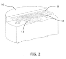
- Fig. 2 shows the electron source of Fig. 1 with deposited material.
- the material which is evaporated due to the hot temperatures of the emission area 12 creates a thin film 13 on the cathode cup surface directly face to face with the emission area 12.
- Fig. 3 shows the separation of deposited material. Due to different applications, the temperature of the cathode cup 10 changes. In case of using different materials for the cathode cup 10 and the electron emitter 11, thermo-mechanical stress due to different thermal expansion coefficients is caused. The resulting shearing force could exceed the adhesion force which leads to a separation 14 of the thin film 13 from the surface of the cathode cup 10. This separation usually starts at the borders of the thin film 13. Depending on the temperature and density distribution within the thin film 13, there is the risk that the thin film 13 bends towards the electron emitter 11 and gets in contact with it. Such a contact would change the electrical path of the current and would thus lead to drastically changed thermal and electrical properties of the electron emitter 11, which would lead to a malfunction of the electron source.
- the inventors of the present invention recognized that it is advantageous to avoid such a separation by changing the adhesion behavior of the thin film with respect to the cathode cup 10.
- a cathode cup comprising a receptacle for holding an electron emitter, wherein the cathode cup is provided at least in the area facing the electron emitter with a surface comprising a plurality of cavities.
- the main reason for the spalling effect caused by different thermal expansion coefficients is the concentration of shearing forces at the end of the thin film and its adhesion on the cathode cup surface being too low.
- the appearance of spalling of the thin film with its possible negative influence on the electron source properties can be overcome with the mentioned embodiment, because in this embodiment the adhesion behavior of the surface facing the electron emitter is increased.
- the cavities are formed in the material of the cathode cup. This provides the advantage that the cavities can be easily formed without too much effort.
- the cavities are formed in a coating covering the cathode cup at least partially.
- the cathode cup surface is covered with the coating and the cavities are formed in the coating afterwards or to cover the cathode cup surface with a coating that already comprises cavities in the form of a structure or a texture of the coating.
- the cavities are created by laser drilling. This manufacturing has the advantage that no sharp edges are generated which would act as stress concentrators, where cracks could be initialized.
- the cavities are created by milling.
- the cavities are created by sink eroding.
- the cavities are formed as depressions, the perimeters of which contact each other. This provides the advantage that the area is utilized optimally for providing the cavities.
- the receptacle comprises a recess within which the electron emitter is arranged and sockets for fixing the electron emitter.
- the cathode cup can act as an electron-optical focusing element.
- the cavities are provided between the sockets.
- This area is the part of the cathode cup which is closest to the part where electrons are emitted and therefore it is advantageous that the cavities are provided in this area.
- the invention provides an electron source and an X-ray system comprising a cathode cup, according to one of the above described embodiments. These devices offer the same advantages as mentioned above.
- the cathode cup is beneficially applicable to any field in which thermionic emitters with high emission currents are necessary.
- the gist of the invention may be seen as the gist of the invention to provide a cathode cup holding an electron emitter with a surface having improved adhesion properties at least in an area facing the electron emitter, in order to avoid the separation of deposited evaporated material.
- Fig. 4 shows an electron source according to a first embodiment of the invention.
- the illustrated electron source comprises a cathode cup 20 having a cylindrical form wherein on a face side (upper side in Fig. 4 ) the cathode cup 20 is provided with a recess having a rectangular cross-sectional area and leading along the diameter of the cylindrical form.
- the bottom face of the recess is provided with two sockets for holding an electron emitter 21.
- the electron emitter 21 is a substantially rectangular flat plate, the center area of which is forming an emitting area 22 which is formed serpentine-like by bringing in cuts having the length of approximately 80 to 90 percent of the width of the electron emitter 21 and which are alternately opened to one side or the other side of the electron emitter 21.
- the emission area 22 Upon applying a voltage to the electron emitter 21, the emission area 22 emits electrons.
- the serpentine-like form decreases the cross-sectional area along the streaming path of the current such that the resistance of the electron emitter is increased in the emitting area 22.
- the electron emitter 21 is provided on a side facing the cathode cup 20 with pins which fit into the sockets of the cathode cup 20.
- the electron emitter 21 can be fixedly held by the cathode cup 20 by fitting the pins into the sockets.
- the electron emitter 21 is made of metal with a high melting point, such as tungsten, lanthanum or their alloys.
- the surface of the cathode cup 20 facing the emitting area 22 is provided with cavities 23 which can be realized by laser drilling, milling or sink welding.
- the cavities 15 are formed between the two sockets in the form of depressions, the perimeter of which contacts each other. Even if this is the preferred form, the cavities 23 can have a plurality of possible forms, for example through holes along a vertical direction in the Figures, counterbores, bole-formed holes, conical holes narrowing to the bottom, cylindrical holes, dents, drillings, grooves, cracks, etc.
- the emitting area 22 Upon application of voltage to the electron emitter 21, the emitting area 22 is heated due to the increased resistance by the current up to temperatures above 2000°C. When this temperature is reached, electrons are emitted and emitter material is evaporated. A thin film deposits on the cathode cup surface that faces the emitting area 22, as described in connection with Fig. 2 . During this operation, the cathode cup 20 reaches temperatures of a few hundred degrees Celsius. When the electron emitter 21 is switched off, the cathode cup 20 cools down and shear-stress within the interface between the thin film of deposited material and the cathode cup 20 results. The stress maximum is located at the borders of the thin film.
- a separation of the thin film from the surface of the cathode cup 20 can be avoided by reducing the maximum shear-stress within the interface between the thin film and the surface of the cathode cup 20.
- Such a reduction of the maximum shear-stress can be achieved by splitting the pure shear-stress in case of a flat surface into a lateral (shearing) and a perpendicular (tensile or comprehensive) component.
- This is realized in this embodiment by structuring the deposition surface with cavities 23, i.e. it is realized by changing the topology of the cathode surface facing the emitter by structuring the surface with cavities having the form as described above.
- the size of the cavities 23 is optimized according to the estimated thickness of the deposited film in such a way that even in case of a film fracture, fragments of the thin film will remain within the cavities 23.
- Fig. 5 shows an electron source according to a second embodiment of the invention.
- This embodiment differentiates from the first embodiment in that the cavities 23 are not directly formed in the material of the cathode cup 20. Instead, the surface of the cathode cup 20 between the two sockets being the area face to face to the emitting area 22 is covered with a coating 24. Either this coating 24 already comprises a texture or a structure before it is applied to the cathode cup 20 which comprises cavities, or the coating 24 is applied to the cathode cup 20 and thereafter the cavities 23 are formed into the coating 24 by means of the processing mentioned in connection with the first embodiment.
Landscapes
- Electron Sources, Ion Sources (AREA)
- Cold Cathode And The Manufacture (AREA)
Description
- The invention relates to a cathode cup as well as an electron source and an X-ray system having such a cathode cup.
- Electron sources are employed for different applications such as X-ray systems like tomography (CT) and cardiovascular (CV) systems. These electron sources usually comprise thermionic emitters which emit electrons upon reaching a certain temperature. The filaments forming these thermionic emitters are necessarily made of metal with a high melting point, like tungsten, lanthanum or their alloys. These thermionic emitters are usually fixed to a cathode cup which primarily acts as an electron-optical focusing element.
- It is an object of the present invention to provide an improved cathode cup, an electron source and an X-ray system.
- This object is solved with a cathode cup, according to the independent claim.
-
Fig. 1 shows an electron source. This electron source comprises acathode cup 10 with a recess in which anelectron emitter 11 is fixedly held. Theelectron emitter 11 is formed as a flat plate with a serpentine likeemission area 12. Upon applying a voltage to theelectron emitter 11, theemission area 12 emits electrons. During the exposure time, theemission area 12 reaches temperatures above 2000°C, in order to emit these electrons. The high temperature has the effect that material of theelectron emitter 11 evaporates and is deposited on cold surfaces around theelectron emitter 11. -
Fig. 2 shows the electron source ofFig. 1 with deposited material. The material which is evaporated due to the hot temperatures of theemission area 12 creates athin film 13 on the cathode cup surface directly face to face with theemission area 12. -
Fig. 3 shows the separation of deposited material. Due to different applications, the temperature of thecathode cup 10 changes. In case of using different materials for thecathode cup 10 and theelectron emitter 11, thermo-mechanical stress due to different thermal expansion coefficients is caused. The resulting shearing force could exceed the adhesion force which leads to aseparation 14 of thethin film 13 from the surface of thecathode cup 10. This separation usually starts at the borders of thethin film 13. Depending on the temperature and density distribution within thethin film 13, there is the risk that thethin film 13 bends towards theelectron emitter 11 and gets in contact with it. Such a contact would change the electrical path of the current and would thus lead to drastically changed thermal and electrical properties of theelectron emitter 11, which would lead to a malfunction of the electron source. - The inventors of the present invention recognized that it is advantageous to avoid such a separation by changing the adhesion behavior of the thin film with respect to the
cathode cup 10. - According to an embodiment of the present invention, there is provided a cathode cup comprising a receptacle for holding an electron emitter, wherein the cathode cup is provided at least in the area facing the electron emitter with a surface comprising a plurality of cavities. The main reason for the spalling effect caused by different thermal expansion coefficients is the concentration of shearing forces at the end of the thin film and its adhesion on the cathode cup surface being too low. The appearance of spalling of the thin film with its possible negative influence on the electron source properties can be overcome with the mentioned embodiment, because in this embodiment the adhesion behavior of the surface facing the electron emitter is increased.
- According to a further embodiment, the cavities are formed in the material of the cathode cup. This provides the advantage that the cavities can be easily formed without too much effort.
- According to another embodiment, the cavities are formed in a coating covering the cathode cup at least partially. In this embodiment it is possible that the cathode cup surface is covered with the coating and the cavities are formed in the coating afterwards or to cover the cathode cup surface with a coating that already comprises cavities in the form of a structure or a texture of the coating.
- According to a further embodiment, the cavities are created by laser drilling. This manufacturing has the advantage that no sharp edges are generated which would act as stress concentrators, where cracks could be initialized.
- Alternatively, the cavities are created by milling.
- As an alternative thereto, the cavities are created by sink eroding.
- According to another embodiment, the cavities are formed as depressions, the perimeters of which contact each other. This provides the advantage that the area is utilized optimally for providing the cavities.
- According to a further embodiment, the receptacle comprises a recess within which the electron emitter is arranged and sockets for fixing the electron emitter. By providing the electron emitter within a recess, the cathode cup can act as an electron-optical focusing element.
- According to a further embodiment, the cavities are provided between the sockets. This area is the part of the cathode cup which is closest to the part where electrons are emitted and therefore it is advantageous that the cavities are provided in this area.
- Further, the invention provides an electron source and an X-ray system comprising a cathode cup, according to one of the above described embodiments. These devices offer the same advantages as mentioned above. The cathode cup is beneficially applicable to any field in which thermionic emitters with high emission currents are necessary.
- These and other aspects of the invention will be apparent from and elucidated with reference to the embodiments described hereafter.
- It may be seen as the gist of the invention to provide a cathode cup holding an electron emitter with a surface having improved adhesion properties at least in an area facing the electron emitter, in order to avoid the separation of deposited evaporated material.
-
- Fig. 1
- shows an electron source;
- Fig. 2
- shows the electron source of
Fig. 1 with deposited material; - Fig. 3
- shows the separation of deposited material;
- Fig. 4
- shows an electron source according to a first embodiment of the invention; and
- Fig. 5
- shows an electron source according to a second embodiment of the invention.
-
Fig. 4 shows an electron source according to a first embodiment of the invention. The illustrated electron source comprises acathode cup 20 having a cylindrical form wherein on a face side (upper side inFig. 4 ) thecathode cup 20 is provided with a recess having a rectangular cross-sectional area and leading along the diameter of the cylindrical form. The bottom face of the recess is provided with two sockets for holding anelectron emitter 21. Theelectron emitter 21 is a substantially rectangular flat plate, the center area of which is forming anemitting area 22 which is formed serpentine-like by bringing in cuts having the length of approximately 80 to 90 percent of the width of theelectron emitter 21 and which are alternately opened to one side or the other side of theelectron emitter 21. Upon applying a voltage to theelectron emitter 21, theemission area 22 emits electrons. For this purpose, the serpentine-like form decreases the cross-sectional area along the streaming path of the current such that the resistance of the electron emitter is increased in the emittingarea 22. Theelectron emitter 21 is provided on a side facing thecathode cup 20 with pins which fit into the sockets of thecathode cup 20. Theelectron emitter 21 can be fixedly held by thecathode cup 20 by fitting the pins into the sockets. Theelectron emitter 21 is made of metal with a high melting point, such as tungsten, lanthanum or their alloys. The surface of thecathode cup 20 facing the emittingarea 22 is provided withcavities 23 which can be realized by laser drilling, milling or sink welding. The cavities 15 are formed between the two sockets in the form of depressions, the perimeter of which contacts each other. Even if this is the preferred form, thecavities 23 can have a plurality of possible forms, for example through holes along a vertical direction in the Figures, counterbores, bole-formed holes, conical holes narrowing to the bottom, cylindrical holes, dents, drillings, grooves, cracks, etc. - Upon application of voltage to the
electron emitter 21, the emittingarea 22 is heated due to the increased resistance by the current up to temperatures above 2000°C. When this temperature is reached, electrons are emitted and emitter material is evaporated. A thin film deposits on the cathode cup surface that faces the emittingarea 22, as described in connection withFig. 2 . During this operation, thecathode cup 20 reaches temperatures of a few hundred degrees Celsius. When theelectron emitter 21 is switched off, thecathode cup 20 cools down and shear-stress within the interface between the thin film of deposited material and thecathode cup 20 results. The stress maximum is located at the borders of the thin film. According to this embodiment, a separation of the thin film from the surface of thecathode cup 20 can be avoided by reducing the maximum shear-stress within the interface between the thin film and the surface of thecathode cup 20. Such a reduction of the maximum shear-stress can be achieved by splitting the pure shear-stress in case of a flat surface into a lateral (shearing) and a perpendicular (tensile or comprehensive) component. This is realized in this embodiment by structuring the deposition surface withcavities 23, i.e. it is realized by changing the topology of the cathode surface facing the emitter by structuring the surface with cavities having the form as described above. The size of thecavities 23 is optimized according to the estimated thickness of the deposited film in such a way that even in case of a film fracture, fragments of the thin film will remain within thecavities 23. -
Fig. 5 shows an electron source according to a second embodiment of the invention. In order to avoid repetitions, only the aspects are described for this embodiment, which differ from the first embodiment. This embodiment differentiates from the first embodiment in that thecavities 23 are not directly formed in the material of thecathode cup 20. Instead, the surface of thecathode cup 20 between the two sockets being the area face to face to the emittingarea 22 is covered with acoating 24. Either thiscoating 24 already comprises a texture or a structure before it is applied to thecathode cup 20 which comprises cavities, or thecoating 24 is applied to thecathode cup 20 and thereafter thecavities 23 are formed into thecoating 24 by means of the processing mentioned in connection with the first embodiment. - While the invention has been illustrated and described in detail in the drawings and foregoing description, such illustration and description are to be considered illustrative or exemplary and not restrictive and it is not intended to limit the invention to the disclosed embodiments. The word "comprising" does not exclude other elements or steps, and the indefinite article "a" or "an" does not exclude a plurality. Any reference signs in the claims should not be construed as limiting the scope of the invention.
Claims (10)
- An electron source comprising:an electron emitter (21), anda cathode cup (20) comprising:a receptacle for holding the electron emitter (21),characterised in that the cathode cup is provided at least in the area facing the electron emitter (21) with a surface comprising a plurality of cavities (23),wherein the receptacle comprises sockets for fixing the electron emitter (21), andwherein the cavities (23) are provided between the sockets.
- The electron source according to claim 1, wherein the cavities (23) are formed in the material of the cathode cup (20).
- The electron source according to claim 1, wherein the cavities (23) are formed in a coating (24) covering the cathode cup (20) at least partially.
- The electron source according to one of the preceding claims, wherein the cavities (23) are created by laser drilling.
- The electron source according to one of claims 1 to 3, wherein the cavities (23) are created by milling.
- The electron source according to one of claims 1 to 3, wherein the cavities (23) are created by sink eroding.
- The electron source according to one of the preceding claims, wherein the cavities (23) are formed as depressions the perimeters of which contact each other.
- The electron source according to one of the preceding claims, wherein the receptacle comprises a recess within which the electron emitter (21) is arranged.
- The electron source according to one of the preceding claims, wherein an area of the electron emitter (21) having an increased electrical resistance is facing the cavities (23).
- An x-ray system comprising an electron source according to one of the preceding claims.
Priority Applications (1)
| Application Number | Priority Date | Filing Date | Title |
|---|---|---|---|
| EP09774972.5A EP2377141B1 (en) | 2008-12-08 | 2009-12-01 | Electron source and cathode cup thereof |
Applications Claiming Priority (3)
| Application Number | Priority Date | Filing Date | Title |
|---|---|---|---|
| EP08170904 | 2008-12-08 | ||
| PCT/IB2009/055432 WO2010067257A1 (en) | 2008-12-08 | 2009-12-01 | Electron source and cathode cup thereof |
| EP09774972.5A EP2377141B1 (en) | 2008-12-08 | 2009-12-01 | Electron source and cathode cup thereof |
Publications (2)
| Publication Number | Publication Date |
|---|---|
| EP2377141A1 EP2377141A1 (en) | 2011-10-19 |
| EP2377141B1 true EP2377141B1 (en) | 2014-07-16 |
Family
ID=41722734
Family Applications (1)
| Application Number | Title | Priority Date | Filing Date |
|---|---|---|---|
| EP09774972.5A Not-in-force EP2377141B1 (en) | 2008-12-08 | 2009-12-01 | Electron source and cathode cup thereof |
Country Status (5)
| Country | Link |
|---|---|
| US (1) | US8548124B2 (en) |
| EP (1) | EP2377141B1 (en) |
| JP (1) | JP5543483B2 (en) |
| CN (1) | CN102246257A (en) |
| WO (1) | WO2010067257A1 (en) |
Families Citing this family (9)
| Publication number | Priority date | Publication date | Assignee | Title |
|---|---|---|---|---|
| US9953797B2 (en) * | 2015-09-28 | 2018-04-24 | General Electric Company | Flexible flat emitter for X-ray tubes |
| JP6744116B2 (en) * | 2016-04-01 | 2020-08-19 | キヤノン電子管デバイス株式会社 | Emitter and X-ray tube |
| DE202017101961U1 (en) | 2017-04-03 | 2018-07-04 | Hofer Mechatronik Gmbh | Traktionsakkumulator, in particular elongate design with adjacently arranged lithium-ion secondary cells |
| EP3386001B1 (en) | 2017-04-03 | 2022-11-23 | hofer powertrain innovation GmbH | Traction accumulator elongated construction with secondary electrochemical cells arranged adjacent to one another and method for controlling the heat management |
| US10636608B2 (en) * | 2017-06-05 | 2020-04-28 | General Electric Company | Flat emitters with stress compensation features |
| JP7021707B2 (en) * | 2018-09-11 | 2022-02-17 | 株式会社島津製作所 | X-ray device |
| US10818466B1 (en) * | 2019-05-01 | 2020-10-27 | GE Precision Healthcare LLC | X-ray tube and cathode cup with deposition shield |
| US11581160B2 (en) | 2020-02-25 | 2023-02-14 | GE Precision Healthcare LLC | Methods and systems for x-ray tube with texturing |
| US20250292986A1 (en) * | 2024-03-18 | 2025-09-18 | GE Precision Healthcare LLC | Flat emitter with compliant supported end |
Family Cites Families (14)
| Publication number | Priority date | Publication date | Assignee | Title |
|---|---|---|---|---|
| NL30158C (en) | 1928-11-17 | |||
| GB496651A (en) | 1936-05-28 | 1938-11-28 | British Thomson Houston Co Ltd | Improvements in and relating to x-ray apparatus |
| US2471298A (en) * | 1943-10-02 | 1949-05-24 | Gen Electric X Ray Corp | Cathode cup construction |
| GB960458A (en) | 1961-06-19 | 1964-06-10 | English Electric Valve Co Ltd | Improvements in or relating to high voltage trigger tubes |
| JPS6063863A (en) | 1983-09-19 | 1985-04-12 | Hitachi Ltd | X-ray tube cathode structure |
| JPH0612598Y2 (en) * | 1987-01-19 | 1994-03-30 | 電気化学工業株式会社 | Hot cathode terminal block |
| FR2633775B1 (en) * | 1988-07-01 | 1995-11-17 | Gen Electric Cgr | RADIOGENIC TUBE WITH FLAT CATHODE AND INDIRECT HEATING |
| JPH05121362A (en) * | 1991-10-25 | 1993-05-18 | Sony Corp | ECR plasma processing equipment |
| DE4325609A1 (en) * | 1993-07-30 | 1995-02-02 | Philips Patentverwaltung | Electron tube |
| US5907595A (en) * | 1997-08-18 | 1999-05-25 | General Electric Company | Emitter-cup cathode for high-emission x-ray tube |
| DE10016125A1 (en) * | 1999-04-29 | 2000-11-02 | Siemens Ag | Thermionic emitter, especially flat emitter for driving X-ray tubes |
| JP4860202B2 (en) * | 2005-08-04 | 2012-01-25 | 浜松ホトニクス株式会社 | X-ray generator |
| ATE525740T1 (en) | 2006-05-11 | 2011-10-15 | Koninkl Philips Electronics Nv | EMITTER DESIGN THAT ALLOWS AN EMERGENCY OPERATION MODE IN CASE OF EMMITTER DAMAGE, FOR USE IN MEDICAL X-RAY TECHNOLOGY |
| JP2007305485A (en) * | 2006-05-12 | 2007-11-22 | Matsushita Electric Ind Co Ltd | Arc discharge apparatus and ion implantation apparatus using the same |
-
2009
- 2009-12-01 CN CN2009801492439A patent/CN102246257A/en active Pending
- 2009-12-01 JP JP2011539150A patent/JP5543483B2/en not_active Expired - Fee Related
- 2009-12-01 US US13/131,906 patent/US8548124B2/en not_active Expired - Fee Related
- 2009-12-01 EP EP09774972.5A patent/EP2377141B1/en not_active Not-in-force
- 2009-12-01 WO PCT/IB2009/055432 patent/WO2010067257A1/en not_active Ceased
Also Published As
| Publication number | Publication date |
|---|---|
| WO2010067257A1 (en) | 2010-06-17 |
| CN102246257A (en) | 2011-11-16 |
| JP5543483B2 (en) | 2014-07-09 |
| US8548124B2 (en) | 2013-10-01 |
| JP2012511234A (en) | 2012-05-17 |
| EP2377141A1 (en) | 2011-10-19 |
| US20110228909A1 (en) | 2011-09-22 |
Similar Documents
| Publication | Publication Date | Title |
|---|---|---|
| US8548124B2 (en) | Electron source and cathode cup thereof | |
| JP5341890B2 (en) | Thermionic electron emitter, method of making a thermionic electron emitter, and x-ray source including a thermionic electron emitter | |
| JP2008533662A (en) | Micro X-ray source | |
| KR102095268B1 (en) | Field Emission X-Ray Source Device | |
| US11915921B2 (en) | Electron source, method for manufacturing same, emitter, and device including same | |
| JP2025072670A (en) | Emitter and device including same | |
| US9928986B2 (en) | Emitter arrangement | |
| US20220093358A1 (en) | X-Ray Tube with Multi-Element Target | |
| US5155755A (en) | Anode for x-ray tubes with composite body | |
| US12633487B2 (en) | Electron source and method for manufacturing same, and emitter and device provided with same | |
| EP4131328B1 (en) | Electron source and method for manufacturing same, and emitter and device provided with same | |
| US12293893B2 (en) | Electron source, manufacturing method therefor, and device comprising electron source | |
| EP4303906B1 (en) | Emitter and device provided with same | |
| EP4503087A1 (en) | Emitter and device comprising same | |
| CN106257614A (en) | Emitter | |
| KR101631668B1 (en) | X-ray source comprising cnt yarn using filtered arc deposition and x-ray emitting apparatus using the same | |
| EP1320117A3 (en) | Method for defect and conductivity engineering of a conducting nanoscaled structure |
Legal Events
| Date | Code | Title | Description |
|---|---|---|---|
| PUAI | Public reference made under article 153(3) epc to a published international application that has entered the european phase |
Free format text: ORIGINAL CODE: 0009012 |
|
| 17P | Request for examination filed |
Effective date: 20110708 |
|
| AK | Designated contracting states |
Kind code of ref document: A1 Designated state(s): AT BE BG CH CY CZ DE DK EE ES FI FR GB GR HR HU IE IS IT LI LT LU LV MC MK MT NL NO PL PT RO SE SI SK SM TR |
|
| DAX | Request for extension of the european patent (deleted) | ||
| RAP1 | Party data changed (applicant data changed or rights of an application transferred) |
Owner name: KONINKLIJKE PHILIPS N.V. Owner name: PHILIPS INTELLECTUAL PROPERTY & STANDARDS GMBH |
|
| GRAP | Despatch of communication of intention to grant a patent |
Free format text: ORIGINAL CODE: EPIDOSNIGR1 |
|
| INTG | Intention to grant announced |
Effective date: 20140129 |
|
| GRAS | Grant fee paid |
Free format text: ORIGINAL CODE: EPIDOSNIGR3 |
|
| GRAA | (expected) grant |
Free format text: ORIGINAL CODE: 0009210 |
|
| AK | Designated contracting states |
Kind code of ref document: B1 Designated state(s): AT BE BG CH CY CZ DE DK EE ES FI FR GB GR HR HU IE IS IT LI LT LU LV MC MK MT NL NO PL PT RO SE SI SK SM TR |
|
| REG | Reference to a national code |
Ref country code: GB Ref legal event code: FG4D |
|
| REG | Reference to a national code |
Ref country code: CH Ref legal event code: EP |
|
| REG | Reference to a national code |
Ref country code: IE Ref legal event code: FG4D |
|
| REG | Reference to a national code |
Ref country code: AT Ref legal event code: REF Ref document number: 678082 Country of ref document: AT Kind code of ref document: T Effective date: 20140815 |
|
| REG | Reference to a national code |
Ref country code: DE Ref legal event code: R096 Ref document number: 602009025366 Country of ref document: DE Effective date: 20140828 |
|
| REG | Reference to a national code |
Ref country code: NL Ref legal event code: VDEP Effective date: 20140716 |
|
| REG | Reference to a national code |
Ref country code: AT Ref legal event code: MK05 Ref document number: 678082 Country of ref document: AT Kind code of ref document: T Effective date: 20140716 |
|
| REG | Reference to a national code |
Ref country code: LT Ref legal event code: MG4D |
|
| PG25 | Lapsed in a contracting state [announced via postgrant information from national office to epo] |
Ref country code: FI Free format text: LAPSE BECAUSE OF FAILURE TO SUBMIT A TRANSLATION OF THE DESCRIPTION OR TO PAY THE FEE WITHIN THE PRESCRIBED TIME-LIMIT Effective date: 20140716 Ref country code: GR Free format text: LAPSE BECAUSE OF FAILURE TO SUBMIT A TRANSLATION OF THE DESCRIPTION OR TO PAY THE FEE WITHIN THE PRESCRIBED TIME-LIMIT Effective date: 20141017 Ref country code: BG Free format text: LAPSE BECAUSE OF FAILURE TO SUBMIT A TRANSLATION OF THE DESCRIPTION OR TO PAY THE FEE WITHIN THE PRESCRIBED TIME-LIMIT Effective date: 20141016 Ref country code: ES Free format text: LAPSE BECAUSE OF FAILURE TO SUBMIT A TRANSLATION OF THE DESCRIPTION OR TO PAY THE FEE WITHIN THE PRESCRIBED TIME-LIMIT Effective date: 20140716 Ref country code: PT Free format text: LAPSE BECAUSE OF FAILURE TO SUBMIT A TRANSLATION OF THE DESCRIPTION OR TO PAY THE FEE WITHIN THE PRESCRIBED TIME-LIMIT Effective date: 20141117 Ref country code: LT Free format text: LAPSE BECAUSE OF FAILURE TO SUBMIT A TRANSLATION OF THE DESCRIPTION OR TO PAY THE FEE WITHIN THE PRESCRIBED TIME-LIMIT Effective date: 20140716 Ref country code: NO Free format text: LAPSE BECAUSE OF FAILURE TO SUBMIT A TRANSLATION OF THE DESCRIPTION OR TO PAY THE FEE WITHIN THE PRESCRIBED TIME-LIMIT Effective date: 20141016 Ref country code: SE Free format text: LAPSE BECAUSE OF FAILURE TO SUBMIT A TRANSLATION OF THE DESCRIPTION OR TO PAY THE FEE WITHIN THE PRESCRIBED TIME-LIMIT Effective date: 20140716 |
|
| PGFP | Annual fee paid to national office [announced via postgrant information from national office to epo] |
Ref country code: GB Payment date: 20141230 Year of fee payment: 6 |
|
| PG25 | Lapsed in a contracting state [announced via postgrant information from national office to epo] |
Ref country code: AT Free format text: LAPSE BECAUSE OF FAILURE TO SUBMIT A TRANSLATION OF THE DESCRIPTION OR TO PAY THE FEE WITHIN THE PRESCRIBED TIME-LIMIT Effective date: 20140716 Ref country code: NL Free format text: LAPSE BECAUSE OF FAILURE TO SUBMIT A TRANSLATION OF THE DESCRIPTION OR TO PAY THE FEE WITHIN THE PRESCRIBED TIME-LIMIT Effective date: 20140716 Ref country code: LV Free format text: LAPSE BECAUSE OF FAILURE TO SUBMIT A TRANSLATION OF THE DESCRIPTION OR TO PAY THE FEE WITHIN THE PRESCRIBED TIME-LIMIT Effective date: 20140716 Ref country code: PL Free format text: LAPSE BECAUSE OF FAILURE TO SUBMIT A TRANSLATION OF THE DESCRIPTION OR TO PAY THE FEE WITHIN THE PRESCRIBED TIME-LIMIT Effective date: 20140716 Ref country code: CY Free format text: LAPSE BECAUSE OF FAILURE TO SUBMIT A TRANSLATION OF THE DESCRIPTION OR TO PAY THE FEE WITHIN THE PRESCRIBED TIME-LIMIT Effective date: 20140716 Ref country code: IS Free format text: LAPSE BECAUSE OF FAILURE TO SUBMIT A TRANSLATION OF THE DESCRIPTION OR TO PAY THE FEE WITHIN THE PRESCRIBED TIME-LIMIT Effective date: 20141116 |
|
| REG | Reference to a national code |
Ref country code: DE Ref legal event code: R097 Ref document number: 602009025366 Country of ref document: DE |
|
| PG25 | Lapsed in a contracting state [announced via postgrant information from national office to epo] |
Ref country code: DK Free format text: LAPSE BECAUSE OF FAILURE TO SUBMIT A TRANSLATION OF THE DESCRIPTION OR TO PAY THE FEE WITHIN THE PRESCRIBED TIME-LIMIT Effective date: 20140716 Ref country code: EE Free format text: LAPSE BECAUSE OF FAILURE TO SUBMIT A TRANSLATION OF THE DESCRIPTION OR TO PAY THE FEE WITHIN THE PRESCRIBED TIME-LIMIT Effective date: 20140716 Ref country code: RO Free format text: LAPSE BECAUSE OF FAILURE TO SUBMIT A TRANSLATION OF THE DESCRIPTION OR TO PAY THE FEE WITHIN THE PRESCRIBED TIME-LIMIT Effective date: 20140716 Ref country code: SK Free format text: LAPSE BECAUSE OF FAILURE TO SUBMIT A TRANSLATION OF THE DESCRIPTION OR TO PAY THE FEE WITHIN THE PRESCRIBED TIME-LIMIT Effective date: 20140716 Ref country code: IT Free format text: LAPSE BECAUSE OF FAILURE TO SUBMIT A TRANSLATION OF THE DESCRIPTION OR TO PAY THE FEE WITHIN THE PRESCRIBED TIME-LIMIT Effective date: 20140716 Ref country code: CZ Free format text: LAPSE BECAUSE OF FAILURE TO SUBMIT A TRANSLATION OF THE DESCRIPTION OR TO PAY THE FEE WITHIN THE PRESCRIBED TIME-LIMIT Effective date: 20140716 |
|
| PLBE | No opposition filed within time limit |
Free format text: ORIGINAL CODE: 0009261 |
|
| STAA | Information on the status of an ep patent application or granted ep patent |
Free format text: STATUS: NO OPPOSITION FILED WITHIN TIME LIMIT |
|
| PGFP | Annual fee paid to national office [announced via postgrant information from national office to epo] |
Ref country code: FR Payment date: 20141230 Year of fee payment: 6 |
|
| 26N | No opposition filed |
Effective date: 20150417 |
|
| PG25 | Lapsed in a contracting state [announced via postgrant information from national office to epo] |
Ref country code: BE Free format text: LAPSE BECAUSE OF NON-PAYMENT OF DUE FEES Effective date: 20141231 |
|
| REG | Reference to a national code |
Ref country code: DE Ref legal event code: R119 Ref document number: 602009025366 Country of ref document: DE |
|
| REG | Reference to a national code |
Ref country code: DE Ref legal event code: R082 Ref document number: 602009025366 Country of ref document: DE Representative=s name: MEISSNER, BOLTE & PARTNER GBR, DE Ref country code: DE Ref legal event code: R081 Ref document number: 602009025366 Country of ref document: DE Owner name: PHILIPS GMBH, DE Free format text: FORMER OWNER: PHILIPS INTELLECTUAL PROPERTY & STANDARDS GMBH, 20099 HAMBURG, DE Ref country code: DE Ref legal event code: R082 Ref document number: 602009025366 Country of ref document: DE Representative=s name: MEISSNER BOLTE PATENTANWAELTE RECHTSANWAELTE P, DE |
|
| PG25 | Lapsed in a contracting state [announced via postgrant information from national office to epo] |
Ref country code: LU Free format text: LAPSE BECAUSE OF FAILURE TO SUBMIT A TRANSLATION OF THE DESCRIPTION OR TO PAY THE FEE WITHIN THE PRESCRIBED TIME-LIMIT Effective date: 20141201 |
|
| REG | Reference to a national code |
Ref country code: CH Ref legal event code: PL |
|
| REG | Reference to a national code |
Ref country code: IE Ref legal event code: MM4A |
|
| PG25 | Lapsed in a contracting state [announced via postgrant information from national office to epo] |
Ref country code: LI Free format text: LAPSE BECAUSE OF NON-PAYMENT OF DUE FEES Effective date: 20141231 Ref country code: IE Free format text: LAPSE BECAUSE OF NON-PAYMENT OF DUE FEES Effective date: 20141201 Ref country code: CH Free format text: LAPSE BECAUSE OF NON-PAYMENT OF DUE FEES Effective date: 20141231 Ref country code: DE Free format text: LAPSE BECAUSE OF NON-PAYMENT OF DUE FEES Effective date: 20150701 |
|
| PG25 | Lapsed in a contracting state [announced via postgrant information from national office to epo] |
Ref country code: SI Free format text: LAPSE BECAUSE OF FAILURE TO SUBMIT A TRANSLATION OF THE DESCRIPTION OR TO PAY THE FEE WITHIN THE PRESCRIBED TIME-LIMIT Effective date: 20140716 |
|
| PG25 | Lapsed in a contracting state [announced via postgrant information from national office to epo] |
Ref country code: SM Free format text: LAPSE BECAUSE OF FAILURE TO SUBMIT A TRANSLATION OF THE DESCRIPTION OR TO PAY THE FEE WITHIN THE PRESCRIBED TIME-LIMIT Effective date: 20140716 |
|
| PG25 | Lapsed in a contracting state [announced via postgrant information from national office to epo] |
Ref country code: MC Free format text: LAPSE BECAUSE OF FAILURE TO SUBMIT A TRANSLATION OF THE DESCRIPTION OR TO PAY THE FEE WITHIN THE PRESCRIBED TIME-LIMIT Effective date: 20140716 |
|
| PG25 | Lapsed in a contracting state [announced via postgrant information from national office to epo] |
Ref country code: MT Free format text: LAPSE BECAUSE OF FAILURE TO SUBMIT A TRANSLATION OF THE DESCRIPTION OR TO PAY THE FEE WITHIN THE PRESCRIBED TIME-LIMIT Effective date: 20140716 Ref country code: HU Free format text: LAPSE BECAUSE OF FAILURE TO SUBMIT A TRANSLATION OF THE DESCRIPTION OR TO PAY THE FEE WITHIN THE PRESCRIBED TIME-LIMIT; INVALID AB INITIO Effective date: 20091201 Ref country code: BE Free format text: LAPSE BECAUSE OF FAILURE TO SUBMIT A TRANSLATION OF THE DESCRIPTION OR TO PAY THE FEE WITHIN THE PRESCRIBED TIME-LIMIT Effective date: 20140716 Ref country code: HR Free format text: LAPSE BECAUSE OF FAILURE TO SUBMIT A TRANSLATION OF THE DESCRIPTION OR TO PAY THE FEE WITHIN THE PRESCRIBED TIME-LIMIT Effective date: 20140716 Ref country code: TR Free format text: LAPSE BECAUSE OF FAILURE TO SUBMIT A TRANSLATION OF THE DESCRIPTION OR TO PAY THE FEE WITHIN THE PRESCRIBED TIME-LIMIT Effective date: 20140716 |
|
| GBPC | Gb: european patent ceased through non-payment of renewal fee |
Effective date: 20151201 |
|
| REG | Reference to a national code |
Ref country code: FR Ref legal event code: ST Effective date: 20160831 |
|
| PG25 | Lapsed in a contracting state [announced via postgrant information from national office to epo] |
Ref country code: GB Free format text: LAPSE BECAUSE OF NON-PAYMENT OF DUE FEES Effective date: 20151201 |
|
| PG25 | Lapsed in a contracting state [announced via postgrant information from national office to epo] |
Ref country code: FR Free format text: LAPSE BECAUSE OF NON-PAYMENT OF DUE FEES Effective date: 20151231 |
|
| PG25 | Lapsed in a contracting state [announced via postgrant information from national office to epo] |
Ref country code: MK Free format text: LAPSE BECAUSE OF FAILURE TO SUBMIT A TRANSLATION OF THE DESCRIPTION OR TO PAY THE FEE WITHIN THE PRESCRIBED TIME-LIMIT Effective date: 20140716 |