EP2375257A2 - Resistive probing tip system for logic analyzer probing systems - Google Patents
Resistive probing tip system for logic analyzer probing systems Download PDFInfo
- Publication number
- EP2375257A2 EP2375257A2 EP11250413A EP11250413A EP2375257A2 EP 2375257 A2 EP2375257 A2 EP 2375257A2 EP 11250413 A EP11250413 A EP 11250413A EP 11250413 A EP11250413 A EP 11250413A EP 2375257 A2 EP2375257 A2 EP 2375257A2
- Authority
- EP
- European Patent Office
- Prior art keywords
- electrical contact
- exposed
- electrical contacts
- carrier
- contact assembly
- Prior art date
- Legal status (The legal status is an assumption and is not a legal conclusion. Google has not performed a legal analysis and makes no representation as to the accuracy of the status listed.)
- Withdrawn
Links
Images













Classifications
-
- G—PHYSICS
- G01—MEASURING; TESTING
- G01R—MEASURING ELECTRIC VARIABLES; MEASURING MAGNETIC VARIABLES
- G01R1/00—Details of instruments or arrangements of the types included in groups G01R5/00 - G01R13/00 and G01R31/00
- G01R1/02—General constructional details
- G01R1/06—Measuring leads; Measuring probes
- G01R1/067—Measuring probes
- G01R1/06772—High frequency probes
-
- G—PHYSICS
- G01—MEASURING; TESTING
- G01R—MEASURING ELECTRIC VARIABLES; MEASURING MAGNETIC VARIABLES
- G01R1/00—Details of instruments or arrangements of the types included in groups G01R5/00 - G01R13/00 and G01R31/00
- G01R1/02—General constructional details
- G01R1/06—Measuring leads; Measuring probes
- G01R1/067—Measuring probes
- G01R1/073—Multiple probes
- G01R1/07307—Multiple probes with individual probe elements, e.g. needles, cantilever beams or bump contacts, fixed in relation to each other, e.g. bed of nails fixture or probe card
- G01R1/07314—Multiple probes with individual probe elements, e.g. needles, cantilever beams or bump contacts, fixed in relation to each other, e.g. bed of nails fixture or probe card the body of the probe being perpendicular to test object, e.g. bed of nails or probe with bump contacts on a rigid support
-
- H—ELECTRICITY
- H01—ELECTRIC ELEMENTS
- H01R—ELECTRICALLY-CONDUCTIVE CONNECTIONS; STRUCTURAL ASSOCIATIONS OF A PLURALITY OF MUTUALLY-INSULATED ELECTRICAL CONNECTING ELEMENTS; COUPLING DEVICES; CURRENT COLLECTORS
- H01R12/00—Structural associations of a plurality of mutually-insulated electrical connecting elements, specially adapted for printed circuits, e.g. printed circuit boards [PCB], flat or ribbon cables, or like generally planar structures, e.g. terminal strips, terminal blocks; Coupling devices specially adapted for printed circuits, flat or ribbon cables, or like generally planar structures; Terminals specially adapted for contact with, or insertion into, printed circuits, flat or ribbon cables, or like generally planar structures
- H01R12/70—Coupling devices
- H01R12/71—Coupling devices for rigid printing circuits or like structures
- H01R12/712—Coupling devices for rigid printing circuits or like structures co-operating with the surface of the printed circuit or with a coupling device exclusively provided on the surface of the printed circuit
- H01R12/714—Coupling devices for rigid printing circuits or like structures co-operating with the surface of the printed circuit or with a coupling device exclusively provided on the surface of the printed circuit with contacts abutting directly the printed circuit; Button contacts therefore provided on the printed circuit
-
- H—ELECTRICITY
- H01—ELECTRIC ELEMENTS
- H01R—ELECTRICALLY-CONDUCTIVE CONNECTIONS; STRUCTURAL ASSOCIATIONS OF A PLURALITY OF MUTUALLY-INSULATED ELECTRICAL CONNECTING ELEMENTS; COUPLING DEVICES; CURRENT COLLECTORS
- H01R13/00—Details of coupling devices of the kinds covered by groups H01R12/70 or H01R24/00 - H01R33/00
- H01R13/66—Structural association with built-in electrical component
- H01R13/665—Structural association with built-in electrical component with built-in electronic circuit
- H01R13/6658—Structural association with built-in electrical component with built-in electronic circuit on printed circuit board
-
- H—ELECTRICITY
- H01—ELECTRIC ELEMENTS
- H01R—ELECTRICALLY-CONDUCTIVE CONNECTIONS; STRUCTURAL ASSOCIATIONS OF A PLURALITY OF MUTUALLY-INSULATED ELECTRICAL CONNECTING ELEMENTS; COUPLING DEVICES; CURRENT COLLECTORS
- H01R13/00—Details of coupling devices of the kinds covered by groups H01R12/70 or H01R24/00 - H01R33/00
- H01R13/66—Structural association with built-in electrical component
- H01R13/6608—Structural association with built-in electrical component with built-in single component
- H01R13/6616—Structural association with built-in electrical component with built-in single component with resistor
Definitions
- the present invention relates to resistive probing tip systems, and more particularly to resistive probing tip systems incorporated into logic analyzer probing systems for highspeed probing of a device under test.
- a prime example is a probe head with pogo pins. These provide adequate compliance, but become an unterminated stub on the circuit being tested. This unterminated stub will reflect energy back into the system under test, so a long time delay in the compliant contact is undesirable. Electrical stubs can impact the circuit being probed, so probe designers seek to minimize the stubs. The ideal probe tip would have a resistive element at the point of contact, thereby creating no stub.
- the SpiritR Compression Test Probe has mounting brackets positioned on either side of parallel rows of contact points on a circuit board of the DUT. Parallel rows of passive resistors corresponding to the parallel rows of contact points on the circuit board are embedded in a connector housing that is positioned between the mounting brackets. Each passive resistor is secured to a lower spring contact and an upper spring contact with the lower spring contact engaging one of the contact points on the circuit board and the upper spring contact engaging a corresponding contact point in a probe head. The stub length of the lower spring contact is 0.100 inches.
- the resistor has resided on a circuit board in the probe head, and the compliant contact comes into contact with the edge of the circuit board.
- the length of the contact and the amount the resistor is set back from the edge of the circuit board both contribute to the unterminated stub length.
- the distance that the resistor is set back from the edge of the circuit board is determined by circuit board manufacturing constraints.
- the edge wrap on the circuit board produces an edge that is somewhat rough and departs from planarity because of the process of routing and plating the laminated circuit board edge. Therefore, there is a need for a resistive probing tip system that enables probing at higher speeds by decreasing the stub length on the probed circuit.
- the present invention provides a resistive probing tip system usable in a logic analyzer probing system that overcomes the above-mentioned disadvantages and drawbacks of the prior art.
- the resistive probing tip system has at least a first carrier and a first electrical contact assembly.
- the first carrier has opposing surfaces with a plurality of resistors engaging the first carrier. Each of the plurality of resistors has opposing electrical contacts that are exposed at respective surfaces of the first carrier.
- the plurality of resistors may be discrete resistors disposed in apertures formed through the first carrier.
- the first carrier may also be a ceramic substrate with the plurality of resistors disposed one or both of the opposing surfaces of the substrate.
- the first electrical contact assembly has opposing surfaces with electrical contacts exposed at the respective opposing surfaces.
- the first electrical contact assembly may be formed using flex circuit material or formed using an elastomeric material having electrically conductive elastomeric contact.
- the first electrical contact assembly may also be formed using a housing having compressible spring contacts disposed therein.
- the first carrier and the first electrical contact assembly selectively mate to and mate from each other with the electrical contacts exposed at one surface of the first carrier and the electrical contacts exposed at one surface of the first electrical contact assembly contacting each other.
- the first carrier and/or the first electrical contact assembly may be selectively secured to either of a circuit board of a device under test or a probe head.
- the resistive probing tip system may also have multiple carriers having opposing surfaces.
- the multiple carriers have the same or similar construction as the first carrier.
- the first carrier and one or more of the multiple carriers selectively mate to and mate from the first electrical contact assembly.
- the electrical contacts exposed at one surface of the respective first carrier and one or more of the multiple carriers contact corresponding electrical contacts exposed at one surface of the first electrical contact assembly.
- the first carrier and one or more of the multiple carriers and/or the first electrical contact assembly may be selectively secured to either of a circuit board of a device under test or a probe head.
- the resistive probing tip system may also have multiple electrical contact assemblies having opposing surfaces.
- the multiple electrical contact assemblies have the same or similar construction as the first electrical contact assembly.
- the electrical contacts exposed at the opposing surfaces of the first electrical contact assembly, one or more of the multiple electrical contact assemblies, the first carrier and one or more of the multiple carriers selectively contact corresponding electrical contacts exposed at the mating opposing surfaces of the first electrical contact assembly, one or more of the multiple electrical contact assemblies, the first carrier and one or more of the multiple carriers.
- the first carrier or the first carrier and one or more of the multiple carriers and/or the first electrical contact assembly and/or the first electrical contact assembly and one or more of the multiple electrical contact assemblies may be selectively secured to either of a circuit board of a device under test or a probe head.
- the resistive probing tip system may be configured with the first carrier or the first and one or more of the multiple carriers disposed between the first electrical contact assembly and a second electrical contact assembly of the multiple electrical contact assemblies.
- a third electrical contact assembly of the multiple electrical contact assemblies may be included that selectively mates to and mates from at least one of the first electrical contact assembly and the second electrical contact assembly.
- a fourth electrical contact assembly of the multiple electrical contact assemblies may be included that selectively mates to and mates from the other of the first electrical contact assembly and the second electrical contact assembly.
- a logic analyzer probing system has a probe head containing at least a first circuit board having electrical contacts thereon and a resistive probing tip system having at least a first carrier and a first electrical contact assembly.
- the first carrier has opposing surfaces with a plurality of resistors engaging the first carrier. Each of the plurality of resistors has opposing electrical contacts that are exposed at respective surfaces of the first carrier.
- the plurality of resistors may be discrete resistors disposed in apertures formed through the first carrier.
- the first carrier may also be a ceramic substrate with the plurality of resistors disposed one or both of the opposing surfaces of the substrate.
- the first electrical contact assembly has opposing surfaces with electrical contacts exposed at the respective opposing surfaces.
- the first electrical contact assembly may be formed using flex circuit material or formed using an elastomeric material having electrically conductive elastomeric contact.
- the first electrical contact assembly may also be formed using a housing having compressible spring contacts disposed therein.
- the first circuit board, the first electrical contact assembly and the first carrier selectively mate to and mate from one another with the electrical contacts exposed at the surfaces of the first circuit board, the first electrical contact assembly and the first carrier contacting corresponding electrical contacts exposed at the mating surfaces of the first circuit board of the probe head, the first electrical contact assembly and the first carrier.
- a housing secures at least one of the first electrical contact assembly and the first carrier between the first circuit board of the probe head and the housing.
- the logic analyzer probing system may also have at least a second electrical contact assembly having opposing surfaces.
- the second electrical contact assembly has the same or similar construction as the first electrical contact assembly.
- the first electrical contact assembly, second electrical contact assembly and the first carrier selectively mate to and mate from one another with the electrical contacts exposed at the opposing surfaces of the first electrical contact assembly, the second electrical contact assembly and the first carrier contacting corresponding electrical contacts exposed at the mating surfaces of the first electrical contact assembly, the second electrical contact assembly and the first carrier.
- the housing receives the second electrical contact assembly or the first carrier for capturing the first carrier, the first electrical contact assembly and the second electrical contact assembly or the first electrical contact assembly and the second electrical contact assembly between the first circuit board of the probe head and the housing.
- the second electrical contact assembly may also be secured to a circuit board of a device under test having a plurality of electrical contacts.
- the electrical contacts exposed at one surface of the second electrical contact assembly selectively mates to and mates from the electrical contacts of the circuit board of the device under test and the electrical contacts exposed at the other surface of the second electrical contact assembly selectively mate to and mate from the electrical contacts of the first carrier or the first electrical contact assembly.
- the probe head of the logic analyzer probing system may also have a second circuit board having electrical contacts thereon and a second carrier.
- the second carrier has the same or similar construction as the first carrier.
- the second circuit board of the probe head, the first electrical contact assembly and the second carrier selectively mate to and mate from one another with the electrical contacts exposed the surfaces of the second circuit board of the probe head, the first electrical contact assembly and the second carrier contacting corresponding electrical contacts exposed at the mating surfaces of the second circuit board of the probe head, the first electrical contact assembly and the second carrier.
- the housing receives the first electrical contact assembly or the first and second carriers for capturing the first electrical contact assembly and the first and second carriers or the first electrical contact assembly or the first and second carriers between the first and second circuit boards of the probe head and the housing.
- a second electrical contact assembly may also be used with a second circuit board in the probe head having electrical contacts thereon and a second electrical contact assembly.
- the second electrical contact assembly has the same or similar construction as the first electrical contact assembly.
- the second electrical contact assembly selectively mates to and mates from the first and second carriers or the first electrical contact assembly with the electrical contacts exposed at the surfaces of the second electrical contact assembly contacting corresponding electrical contacts exposed at the mating surfaces of the first and second carriers or the first electrical contact assembly.
- the housing receives the second electrical contact assembly or the first and second carriers for capturing the first and second carriers, the first electrical contact assembly and the second electrical contact assembly or the first electrical contact assembly and the second electrical contact assembly between the first and second circuit boards of the probe head and the housing.
- the second electrical contact assembly may also be secured to a circuit board of a device under test having a plurality of electrical contacts.
- the electrical contacts exposed at one surface of the second electrical contact assembly selectively mates to and mates from the electrical contacts of the circuit board of the device under test and the electrical contacts exposed at the other surface of the second electrical contact assembly selectively mate to and mate from the electrical contacts of the first and second carriers or the first electrical contact assembly.
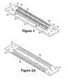
- Figure 1 is an exploded perspective view of a first embodiment of a carrier receiving discrete resistive elements usable in a resistive probing tip system according to the present invention.
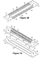
- Figures 2A and 2B are perspective views of a second embodiment of a carrier having resistive elements and electrical contacts formed thereon usable in a resistive probing tip system according to the present invention.
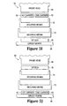
- Figure 3A is an exploded perspective view of a first embodiment of an electrical contact assembly usable in a resistive probing tip system according to the present invention.
- Figure 3B is a perspective view of a second embodiment of an electrical contact assembly usable in a resistive probing tip system according to the present invention.
- Figure 4 an exploded perspective view of an electrical contact assembly and first and second carriers usable in a resistive probing tip system according to the present invention.
- Figures 5A through 5L are various configurations using an electrical contact assembly and first or first and second carriers and in the resistive probing tip system according to the present invention.
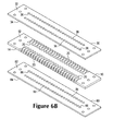
- Figure 6A through 6C are exploded perspective views of a carrier and first and second electrical contact assemblies usable in a resistive probing tip system according to the present invention.
- Figures 7A through 7L are various configurations using first and second electrical contact assemblies and a carrier in the resistive probing tip system according to the present invention.
- Figure 8A through 8C are exploded perspective views of a carrier and first, second and third electrical contact assemblies usable in a resistive probing tip system according to the present invention.
- Figures 9A through 9J are various configurations using first, second and third electrical contact assemblies and a carrier in the resistive probing tip system according to the present invention.
- Figure 10A through 10C are exploded perspective views of a carrier and first, second, third and fourth electrical contact assemblies usable in a resistive probing tip system according to the present invention.
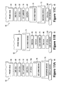
- Figures 11A through 11F are various configurations using first, second, third and fourth electrical contact assemblies and a carrier in the resistive probing tip system according to the present invention.
- Figure 12 is a first example of a logic analyzer probing system using the resistive probing tip system of the present invention.
- Figure 13 is a second example of a logic analyzer probing system using the resistive probing tip system of the present invention.
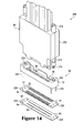
- Figure 14 is a third example of a logic analyzer probing system using the resistive probing tip system of the present invention.
- Figure 15 is a fourth example of a logic analyzer probing system using the resistive probing tip system of the present invention.
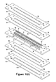
- Figure 16 is another example of a logic analyzer probing system using the resistive probing tip system of the present invention.
- FIG. 1 there is shown an exploded perspective view of a carrier 10 usable in a resistive probing tip system according to the present invention.
- the carrier 10 may be formed as a planar body having opposing surfaces 12 and 14 using a non-conductive material, such a plastic, elastomer, and the like.
- Apertures 16 are formed through the carrier 10 that extend to the opposing surfaces 12, 14.
- Discrete resistive elements 18 having electrical contacts 20 at opposing ends thereof are disposed in the apertures 16 with the electrical contacts 20 of the discrete resistive elements 18 exposed at the opposing surfaces 12, 14 of the carrier 10.
- Discrete resistive elements 18 that are suitable for use in carrier 10 include the CRCW0402 and CRCW0201 Thick Film, Rectangular Chip Resistors, manufactured and sold by Vishay Intertechnolgy, Inc., Malvern, Pennsylvania.
- a carrier 10 formed of elastomer preferably should have a durometer of approximately 70 (Shore A) in the current embodiment in order to both retain the resistive elements 18 and permit individual compliance of each resistive element 18. However, a durometer ranging from approximately 50 to approximately 100 would also be suitable.
- FIGS 2A and 2B shows perspective top and bottom views of another carrier 10 that may be formed as a substrate using a ceramic material or the like.
- the ceramic substrate carrier 10 has opposing surfaces 12, 14 with electrical contacts 20 formed on the opposing surfaces 12, 14.
- Resistive elements 22 are formed on the ceramic substrate carrier 10 with each end of the resistive elements 22 being coupled to an electrical contact 20.
- the resistive elements 22 and electrical contacts 20 are formed using well-known thick film, thin film, or other technologies.
- One of the electrical contacts 20 of each resistive element 22 is formed on one of the opposing surfaces 12, 14 of the ceramic substrate carrier 10 and the other electrical contact 20 of each resistive element 22 is formed on the other of the opposing surface 12, 14 of the ceramic substrate carrier 10.
- the electrical contacts 20 may be formed on the opposing side surfaces of the ceramic substrate carrier 10 with this alternative being equivalent to the electrical contacts 20 being formed on the opposing flat surfaces 12, 14 of the ceramic substrate carrier 10.
- a further alternative has the resistive elements 22 formed of discrete resistors with one end of each discrete resistor connected to an electrical contact 20 formed on one of the opposing side surfaces of the ceramic substrate carrier 10 and the other end of each discrete resistor connected to an electrical contact 20 formed on the other of the side surfaces of the ceramic substrate carrier 10.
- the resistive probing tip system has at least a first electrical contact assembly (first ECA) 30 as shown in Figures 3A and 3B .
- the electrical contact assembly 30 has opposing surfaces 32 and 34 with electrical contacts 36 exposed at the opposing surfaces 32, 34. Each electrical contact 36 exposed at one of the opposing surfaces 32, 34 is electrically coupled to a corresponding electrical contact 36 exposed at the other opposing surface.
- the electrical contacts 36 exposed at the opposing surfaces 32, 34 correspond to the electrical contacts 20 of the resistive elements 18, 22 exposed at the opposing surfaces 12, 14 of the carrier 10.
- the electrical contact assembly 30 is formed of a flex circuit material 38 having corresponding electrical contacts 36 formed on the opposing surfaces 32, 34 and coupled together by electrically conductive through vias.
- the flex circuit material 38 has a thickness on the order of 0.010 inches.
- the electrical contact assembly may be formed of an elastomeric material having electrically conductive contacts formed through the elastomeric material.
- multiple fine electrical wires form each of the electrical contacts with the fine electrical wires extending to the opposing surfaces 32, 34 of the electrical contact assembly 30.
- the elastomeric material has a free height on the order of 0.039 inches and a compressed height of 0.031 inches.
- Figure 3B show a further embodiment of the electrical contact assembly 30 where metal spring electrical contacts 36 are disposed in a housing 40 with the ends of the metal spring electrical contacts extending from apertures 42 formed in the opposing surfaces 32, 34 of the electrical contact assembly 30.
- metal spring electrical contacts usable in the electrical contact assembly 30 are RC Spring Probes manufactured and sold by Ardent Concepts, Inc., Hampton Beach, New Hampshire.
- the free height of the metal spring electrical contact is 0.036 inches.
- the compressed height is 0.031 inches which is set by the thickness of the housing 40 of the electrical contact assembly 30.
- Figure 4 show an alternative embodiment for the resistive probing tip system according to the present invention.
- the embodiment of Figure 4 has first and second carriers 50 and 52.
- the carriers 50, 52 are ceramic substrates having resistive elements 54 formed thereon. Electrical contacts 56 are formed on the ends of the resistive elements 54 with the electrical contacts 56 extending over the opposing side surfaces 58 and 60 of the ceramic substrate carriers 50, 52.
- the resistive elements 54 and electrical contacts 56 are formed using well-known thick film, thin film, or other technologies.
- the resistive elements 54 may be discrete resistors having opposing electrical contact 56 that are secured to a carrier 50, 52, such as a circuit board.
- the electrical contacts 56 of the discrete resistors 54 extend above opposing surfaces of the circuit board.
- the carrier or carriers 10, 50, 52 and/or the first ECA 30 may be secured to a probe head 64 of a logic analyzer probe or secured to a circuit board 66 of a device under test.
- the probe head 64 has at least a first circuit board (not shown) having electrical contacts corresponding to the resistive elements 18, 22, 54 of the carrier or carriers 10, 50, 52.
- the electrical contacts 20, 56 exposed at one of the opposing surfaces 12, 14, 58, 60 of the carrier or carriers 10, 50, 52 selectively mate to and mate from the electrical contacts 36 exposed at one of the opposing surfaces 32, 34 of the first ECA 30.
- the electrical contacts 20, 56 exposed at the other of the opposing surface 12, 14, 58, 60 of the carrier or carriers 10, 50, 52 or the electrical contacts 36 exposed at the other of the opposing surfaces 32, 34 of the first ECA 30 selectively mate to and mate from the electrical contacts on the circuit board of the probe head 64.
- the electrical contacts 20, 56 exposed at the other of the opposing surface 12, 14, 58, 60 of the carrier or carriers 10, 50, 52 or the electrical contacts 36 exposed at the other of the opposing surfaces 32, 34 of the first ECA 30 selectively mate to and mate from the electrical contacts on the circuit board 66 of the device under test.
- the capability of the carrier 10 or carriers 50, 52 and the first ECA 30 to selectively mate to and mate with one another and mate to and mate from the circuit board of the probe head 64 and/or the circuit board 66 of the device under test allows the selective replacement of the carrier or carriers and electrical contact assembly to be selectively replaced if one of them becomes inoperative.
- the first carrier 10 and the first ECA 30 are secured to the probe head 64 by a housing 70 mating with the probe head 64.
- the electrical contacts 20 exposed at one of the opposing surfaces 12, 14 of the first carrier 10 contact the electrical contacts on the circuit board in the probe head 64.
- the electrical contacts 36 exposed at one of the opposing surfaces 32, 34 of the first ECA 30 contact the electrical contacts on the circuit board 66 of the device under test when the probe head 64 is secured to the circuit board 66 of the device under test using a securing means, such as a logic probe socket housing 72.
- the electrical contacts 20 exposed at the other of the opposing surfaces 12, 14 of the first carrier 10 contact corresponding electrical contacts 36 exposed at the other of the opposing surfaces 32, 34 of the first ECA 30.
- the first carrier 10 is secured to the probe head 64 by the housing 70 and the first ECA 30 is secured to the circuit board 66 of the device under test by the socket housing 72.
- the electrical contacts 20 exposed at one of the opposing surfaces 12, 14 of the first carrier 10 contact the electrical contacts on the circuit board in the probe head 64.
- the electrical contacts 36 exposed at one of the opposing surfaces 32, 34 of the first ECA 30 contact the electrical contacts on the circuit board 66 of the device under test.
- the electrical contacts 20 exposed at the other of the opposing surfaces 12, 14 of the first carrier 10 contact corresponding electrical contacts 36 exposed at the other of the opposing surfaces 32, 34 of the first ECA 30 when the probe head 64 is inserted into the socket housing 72 on the circuit board 66.
- the first ECA 30 is secured to the probe head 64 by the housing 70 and the first carrier 10 is secured to the circuit board 66 of the device under test by the socket housing 72.
- the electrical contacts 36 exposed at one of the opposing surfaces 32, 34 of the first ECA 30 contact the electrical contacts on the circuit board in the probe head 64.
- the electrical contacts 20 exposed at one of the opposing surfaces 12, 14 of the first carrier 10 contact the electrical contacts on the circuit board 66 of the device under test.
- the electrical contacts 36 exposed at the other of the opposing surfaces 32, 34 of the first ECA 30 contact corresponding electrical contacts 20 exposed at the other of the opposing surfaces 12, 14 of the first carrier 10 when the probe head 64 is inserted into the socket housing 72 on the circuit board 66.
- the first carrier 10 and the first ECA 30 are secured to the circuit board 66 of the device under test by the socket housing 72.
- the electrical contacts 20 exposed at one of the opposing surfaces 12, 14 of the first carrier 10 contact the electrical contacts 36 exposed at the one of the opposing surfaces 32, 34 of the first ECA 30.
- the electrical contacts 36 exposed at the other of the opposing surfaces 32, 34 of the first ECA 30 contact the electrical contacts on the circuit board 66 of the device under test.
- the electrical contacts 20 exposed at the other of the opposing surfaces 12, 14 of the first carrier 10 contact corresponding the electrical contacts on the circuit board in the probe head 64 when the probe head 64 is inserted into the socket housing 72 on the circuit board 66.
- the positions of the first carrier 10 and the first ECA 30 are reversed.
- the first ECA 30 and the first carrier 10 are secured to the circuit board 66 of the device under test by the socket housing 72.
- the electrical contacts 36 exposed at one of the opposing surfaces 32, 34 of the first ECA 30 contact the electrical contacts 20 exposed at the one of the opposing surfaces 12, 14 of the first carrier 10.
- the electrical contacts 20 exposed at the other of the opposing surfaces 12, 14 of the first carrier 10 contact the electrical contacts on the circuit board 66 of the device under test.
- the electrical contacts 36 exposed at the other of the opposing surfaces 32, 34 of the first ECA 30 contact corresponding the electrical contacts on the circuit board in the probe head 64 when the probe head 64 is inserted into the socket housing 72 on the circuit board 66.
- first and second carriers 50, 52 and the first ECA 30 are secured to the probe head 64 by the housing 70 mating with the probe head 64.
- the electrical contacts 56 exposed at one of the opposing surfaces 58, 60 of the respective first and second carriers 50, 52 contact the electrical contacts on first and second circuit boards (not shown) in the probe head 64.
- the electrical contacts 56 exposed at the other opposing surfaces 58, 60 of the respective first and second carriers 50, 52 contact corresponding electrical contacts 36 on one of the opposing surfaces 32, 34 of the first ECA 30.
- the electrical contacts 36 exposed at the other of opposing surfaces 32, 34 of the first ECA 30 contact the electrical contacts on the circuit board 66 of the device under test when the probe head 64 is inserted into the socket housing 72 on the circuit board 66.
- the probe head 64 is mounted to the circuit board 66 using a securing means, such as a logic probe socket 72.
- the first and second carriers 50, 52 are secured to the probe head 64 by the housing 70 and the first ECA 30 is secured to the circuit board 66 of the device under test by the socket housing 72.
- the electrical contacts 56 exposed at one of the opposing surfaces 58, 60 of the respective first and second carriers 50, 52 contact the electrical contacts on the first and second circuit boards in the probe head 64.
- the electrical contacts 36 exposed at one of the opposing surfaces 32, 34 of the first ECA 30 contact the electrical contacts on the circuit board 66 of the device under test.
- the electrical contacts 56 exposed at the other of the opposing surfaces 58, 60 of the first and second carriers 50, 52 contact corresponding electrical contacts 36 exposed at the other of the opposing surfaces 32, 34 of the first ECA 30 when the probe head 64 is inserted into the socket housing 72 on the circuit board 66.
- the first ECA 30 is secured to the probe head 64 by the housing 70 and the first and second carriers 50, 52 are secured to the circuit board 66 of the device under test by the socket housing 72.
- the electrical contacts 36 exposed at one of the opposing surfaces 32, 34 of the first ECA 30 contact the electrical contacts on the first and second circuit board in the probe head 64.
- the electrical contacts 56 exposed at one of the opposing surfaces 58, 60 of the respective first and second carriers 50, 52 contact the electrical contacts on the circuit board 66 of the device under test.
- the electrical contacts 36 exposed at the other of the opposing surfaces 32, 34 of the first ECA 30 contact corresponding electrical contacts 56 exposed at the other of the opposing surfaces 58, 60 of the respective first and second carriers 50, 52 when the probe head 64 is inserted into the socket housing 72 on the circuit board 66.
- the first and second carriers 50, 52 and the first ECA 30 are secured to the circuit board 66 of the device under test by the socket housing 72.
- the electrical contacts 56 exposed at one of the opposing surfaces 58, 60 of the first and second carriers 50, 52 contact corresponding electrical contacts 36 exposed at one of the opposing surfaces 32, 34 of the first ECA 30.
- the electrical contacts 36 exposed at the other of the opposing surfaces 32, 34 of the first ECA 30 contact the electrical contacts on the circuit board 66 of the device under test.
- the electrical contacts 56 exposed at the other of the opposing surfaces 58, 60 of the respective first and second carriers 50, 52 contact the electrical contacts on first and second circuit boards in the probe head 64 when the probe head 64 is inserted into the socket housing 72 on the circuit board 66.
- the first ECA 30 and the first and second carriers 50, 52 are secured to the circuit board 66 of the device under test by the socket housing 72.
- the electrical contacts 36 exposed at one of the opposing surfaces 32, 34 of the first ECA 30 contact corresponding electrical contacts 56 exposed at one of the opposing surfaces 58, 60 of the first and second carriers 50, 52.
- the electrical contacts 56 exposed at the other of the opposing surfaces 58, 60 of the respective first and second carriers 50, 52 contact the electrical contacts on the circuit board 66 of the device under test.
- the electrical contacts 36 exposed at the other of the opposing surfaces 32, 34 of the first ECA 30 contact the electrical contacts on the first and second circuit boards of the probe head 64 when the probe head 64 is inserted into the socket housing 72 on the circuit board 66.
- Figures 6A , 6B and 6C show further configurations of the resistive probing tip system 62 according to the present invention.
- Figure 6A show the carrier 10 of Figure 1 disposed between the first ECA 30 and a second electrical contact assembly (second ECA) 80.
- the carrier 10 has opposing surface 12, 14 with discrete resistors 18 disposed in apertures 16 formed in the carrier 10. Electrical contacts 20 formed on the opposing ends of the discrete resistors 18 are exposed at the opposing surfaces 12, 14.
- Figures 6B and 6C show perspective top and bottom views of the previously described ceramic substrate carrier 10 disposed between the first ECA 30 and the second ECA 80.
- the ceramic substrate carrier 10 has opposing surfaces 12, 14 with electrical contacts 20 formed on the opposing surfaces.
- Resistive elements 22 are formed on the ceramic substrate carrier 10 with each resistive element 22 having one end connected to one of the electrical contacts 20 on one of the opposing surfaces 12, 14 and the other end of each resistive element 22 connected to one of the electrical contacts 20 on the other opposing surface 12, 14 of the ceramic substrate carrier 10.
- the second ECA 80 has opposing surfaces 82 and 84 with electrical contacts 86 being exposed at the opposing surfaces 82, 84. Each electrical contact 86 exposed at one of the opposing surfaces 82, 84 of the second ECA 80 is electrically coupled to a corresponding electrical contact 86 exposed at the other opposing surface 82, 84.
- the second ECA 80 is formed in the same manner as previously described for the first ECA 30.
- the electrical contacts 20 exposed at the opposing surfaces 12, 14 of the first carrier 10 selectively mate to and mate from the electrical contacts 36 exposed at one of the opposing surfaces 32, 34 of the first ECA 30 and the electrical contacts 86 exposed at one of the opposing surfaces 82, 84 of the second ECA 80.
- the electrical contacts 20 exposed at one of the opposing surface 12, 14 of the carrier 10 or the electrical contacts 36 exposed at one of the opposing surfaces 32, 34 of the first ECA 30 selectively mate to and mate from the electrical contacts on the circuit board of the probe head 64.
- the electrical contacts 20 exposed at one of the opposing surface 12, 14 of the carrier 10 or the electrical contacts 86 exposed at one of the opposing surfaces 82, 84 of the second ECA 80 selectively mate to and mate from the electrical contacts on the circuit board 66 of the device under test.
- Figures 7A-7L show various configurations of the resistive probing tip system 62 according to the present invention having the first ECA 30 and second ECA 80.
- the first carrier 10, the first ECA 30 and the second ECA 80 may be secured to the probe head 64 of a logic analyzer probe or secured to the circuit board 66 of a device under test.
- Further configurations include one of the first ECA 30 or the first carrier 10 being secured to the probe head 64 of a logic analyzer probe or secured to the circuit board 66 of a device under test.
- the first carrier 10 or one of the first ECA 30 and the second ECA 80 may be secured to the probe head 64 or to the circuit board 66 of the device under test.
- the first ECA 30 and second ECA 80 are secured to the probe head 64 by the housing 70 mating with the probe head 64.
- the electrical contacts 36 exposed at one of the opposing surfaces 32, 34 of the first ECA 30 contact the electrical contacts on the circuit board in the probe head 64.
- the electrical contacts 86 exposed at one of the opposing surfaces 82, 84 of the second ECA 80 contact the electrical contacts on the circuit board 66 of the device under test when the probe head 64 is inserted into the socket housing 72 on the circuit board 66.
- the electrical contacts 20 exposed at one of the opposing surfaces 12, 14 of the first carrier 10 contact corresponding electrical contacts 36 exposed at the other of the opposing surfaces 32, 34 of the first ECA 30.
- the electrical contacts 20 exposed at the other of the opposing surfaces 12, 14 of the first carrier 10 contact the electrical contacts 86 exposed at the other of the opposing surfaces 82, 84 of the second ECA 80.
- the first carrier 10 is position adjacent to the probe head.
- the electrical contacts 20 exposed at one of the opposing surfaces 12, 14 of the first carrier 10 contact the electrical contacts on the circuit board in the probe head 64.
- the electrical contacts 86 exposed at one of the opposing surfaces 82, 84 of the second ECA 80 contact the electrical contacts on the circuit board 66 of the device under test when the probe head 64 is inserted into the socket housing 72 on the circuit board 66.
- the electrical contacts 36 exposed at one of the opposing surfaces 32, 34 of the first ECA 30 contact corresponding electrical contacts 20 exposed at the other of the opposing surfaces 12, 14 of the first carrier 10.
- the electrical contacts 36 exposed at the other of the opposing surfaces 32, 34 of the first ECA 30 contact corresponding electrical contacts 86 exposed at the other of the opposing surface 82, 84 of the second ECA 80.
- the first carrier 10, the first ECA 80 and second ECA 80 are secured to the circuit board 66 of the device under test by the socket housing 72.
- the electrical contacts 36 exposed at one of the surfaces 32, 34 of the first ECA 30 contact the electrical contacts on the circuit board in the probe head 64 when the probe head 64 is inserted into the socket housing 72 on the circuit board 66.
- the electrical contacts 86 exposed at one of the opposing surfaces 82, 84 of the second ECA 80 contact the electrical contacts on the circuit board 66 of the device under test.
- the electrical contacts 20 exposed at one of the opposing mating surfaces 12, 14 of the first carrier 10 contact corresponding electrical contacts 36 exposed at the other of the opposing surfaces 32, 34 of the first ECA 30.
- the electrical contacts 20 exposed at the other of the opposing surfaces 12, 14 of the first carrier 10 contact corresponding electrical contacts 86 exposed at the other of the opposing surfaces 82, 84 of the second ECA 80.
- the first ECA 30 and the first carrier 10 are reversed.
- the electrical contacts 20 exposed at one of the surfaces 12, 14 of the first carrier 10 contact the electrical contacts on the circuit board in the probe head 64 when the probe head 64 is inserted into the socket housing 72 on the circuit board 66.
- the electrical contacts 86 exposed at one of the opposing surfaces 82, 84 of the second ECA 80 contact the electrical contacts on the circuit board 66 of the device under test.
- the electrical contacts 36 exposed at one of the opposing surfaces 32, 34 of the first ECA 30 contact corresponding electrical contacts 20 exposed at the other of the opposing surfaces 12, 14 of the first carrier 10.
- the electrical contacts 36 exposed at the other of the opposing surfaces 32, 34 of the first ECA 30 contact corresponding electrical contacts 86 exposed at the other of the opposing surfaces 82, 84 of the second ECA 80.
- the first carrier 10 is positioned on the circuit board 66 of the device under test.
- the electrical contacts 36 exposed at one of the opposing surfaces 32, 34 of the first ECA 30 contact the electrical contacts on the circuit board in the probe head 64 when the probe head 64 is inserted into the socket housing 72 on the circuit board 66.
- the electrical contacts 20 exposed at one of the opposing surfaces 12, 14 of the first carrier 10 contact the electrical contacts on the circuit board 66 of the device under test.
- the electrical contacts 86 exposed at one of the opposing surfaces 82, 84 of the second ECA 80 contact corresponding electrical contacts 30 exposed at the other of the opposing surfaces 32, 34 of the first ECA 30.
- the electrical contacts 86 exposed at the other of the opposing surfaces 82, 84 of the second ECA 80 contact corresponding electrical contacts 20 exposed at the other of the opposing surfaces 12, 14 of the first carrier 10.
- the first ECA 30 and the first carrier 10 are secured to the probe head 64 by the housing 70 mating with the probe head 64 and the second ECA 80 is secured to the circuit board 66 of the device under test by the socket housing 72.
- the electrical contacts 36 exposed at one of the opposing surfaces 32, 34 of the first ECA 30 contact the electrical contacts on the circuit board of the probe head 64.
- the electrical contact 86 exposed at one of the opposing surfaces 82, 84 of the second ECA 80 contact the electrical contacts on the circuit board 66 of the device under test.
- the electrical contacts 20 exposed at one of the opposing surfaces 12, 14 of the first carrier 10 contact corresponding electrical contacts 36 exposed at the other of the opposing surfaces 32, 34 of the first ECA 30.
- the electrical contacts 20 exposed at the other of the opposing surfaces 12, 14 of the first carrier 10 contact corresponding electrical contacts 86 exposed at the other of the opposing surfaces 82, 84 of the second ECA 80 when the probe head 64 is inserted into the socket housing 72 on the circuit board 66.
- the electrical contacts 36 exposed at the other of the opposing surfaces 32, 34 of the first ECA 30 contact corresponding electrical contacts 86 exposed at the other of the opposing surfaces 82, 84 of the second ECA 80 when the probe head 64 is inserted into the socket housing 72 on the circuit board 66.
- first ECA 30 and the second ECA 80 are secured to the probe head 64 by the housing 70 mating with the probe head 64 and the first carrier 10 is secured to the circuit board 66 of the device under test by the socket housing 72.
- the electrical contacts 36 exposed at one of the opposing surfaces 32, 34 of the first ECA 30 contact the electrical contacts on the circuit board of the probe head 64.
- the electrical contacts 20 exposed at one of the opposing surfaces 12, 14 of the first carrier 10 contact the electrical contacts on the circuit board 66 of the device under test.
- the electrical contacts 86 exposed at one of the opposing surfaces 82, 84 of the second ECA 80 contact corresponding electrical contacts 36 exposed at the other of the opposing surfaces 32, 34 of the first ECA 30.
- the electrical contacts 86 exposed at the other of the opposing surfaces 82, 84 of the second ECA 80 contact corresponding electrical contacts 20 exposed at the other of the opposing surfaces 12, 14 of the first carrier 10 when the probe head 64 is inserted into the socket housing 72 on the circuit board 66.
- the first ECA 30 is secured to the probe head 64 by the housing 70 mating with the probe head 64 and the first carrier 10 and the second ECA 80 are secured to the circuit board 66 of the device under test by the socket housing 72.
- the electrical contacts 36 exposed at one of the opposing surfaces 32, 34 of the first ECA 30 contact the electrical contacts on the circuit board of the probe head 64.
- the electrical contacts 86 exposed at one of the opposing surfaces 82, 84 of the second ECA 80 contact the electrical contacts on the circuit board 66 of the device under test.
- the electrical contacts 20 exposed at one of the opposing surfaces 12, 14 of the first carrier 10 contact corresponding electrical contacts 36 exposed at the other of the opposing surfaces 32, 34 of the first ECA 30 when the probe head 64 is inserted into the socket housing 72 on the circuit board 66.
- the electrical contacts 20 exposed at the other of the opposing surfaces 12, 14 of the first carrier 10 contact corresponding electrical contacts 86 exposed at the other of the opposing surfaces 82, 84 of the second ECA 80.
- the first carrier 10 is secured to the probe head 64 by the housing 70 mating with the probe head 64 and the first ECA 30 and the second ECA 80 are secured to the circuit board 66 of the device under test by the socket housing 72.
- the electrical contacts 20 exposed at one of the opposing surfaces 12, 14 of the carrier 10 contact the electrical contacts on the circuit board of the probe head 64.
- the electrical contacts 86 exposed at one of the opposing surfaces 82, 84 of the second ECA 80 contact the electrical contacts on the circuit board 66 of the device under test.
- the electrical contacts 36 exposed at one of the opposing surfaces 32, 34 of the first ECA 30 contact corresponding electrical contacts 20 exposed at the other of the opposing surfaces 12, 14 of the first carrier 10 when the probe head 64 is inserted into the socket housing 72 on the circuit board 66.
- the electrical contacts 36 exposed at the other of the opposing surfaces 32, 34 of the first ECA 30 contact corresponding electrical contacts 86 exposed at the other of the opposing surfaces 82, 84 of the second ECA 80.
- FIGS 8A , 8B and 8C show a further configuration of the resistive probing tip system 62 according to the present invention having a third electrical contact assembly (third ECA) 90.
- the third ECA 90 has opposing surfaces 92 and 94 with electrical contacts 96 being exposed at the opposing surfaces 92, 94.
- Each electrical contact 96 exposed at one of the opposing surfaces 92, 94 of the third ECA 90 is electrically coupled to a corresponding electrical contact 96 exposed at the other opposing surface 92, 94.
- the third ECA 90 is formed in the same manner as previously described for the first ECA 30.
- the third ECA 90 is preferably positioned so that the electrical contacts 96 exposed at one of the opposing surfaces 92, 94 selectively mate to and mate from the electrical contacts 36 exposed at one of the opposing surfaces 32, 34 of the first ECA 30, as shown in Figure 8A , or the corresponding electrical contacts 86 exposed at one of the opposing surfaces 82, 84 of the second ECA 80, as shown in figures 8B and 8C .
- the electrical contacts 96 exposed at one of the opposing surface 92, 94 of the third ECA 90 may selectively mate to and mate from the electrical contacts on the circuit board of the probe head 64 or the electrical contacts on the circuit board 66 of the device under test.
- Figures 9A-9J show various configurations of the resistive probing tip system 62 according to the present invention having the third ECA 90.
- the first carrier 10, the first ECA 30, the second ECA 80 and the third ECA 90 may be secured to the probe head 64 of a logic analyzer probe or secured to the circuit board 66 of a device under test.
- Further configurations include the carrier 10 and the first ECA 30 and the second ECA80 being secured to the probe head 64 of the logic analyzer probe and the third ECA 90 secured to the circuit board 66 of the device under test.
- Additional configurations secure the first ECA 30 or the third ECA 90 to the probe head 64 of the logic analyzer probe and secure the corresponding first carrier 10, the second ECA 80 and the third ECA 90 or the carrier 10, the first ECA 30 and the second ECA 80 to the circuit board 66 of the device under test.
- the first carrier 10 and the first ECA 30 or the first ECA 30 and third ECA 90 may be secured to the probe head 64 of the logic analyzer probe and the corresponding second ECA 80 and the third ECA 90 or the first carrier 10 and the second ECA 80 may be secured to the circuit board 66 of the device under test.
- the first carrier 10, the first ECA 30, the second ECA 80 and the third ECA 90 are secured to the probe head 64 by the housing 70 mating with the probe head 64.
- the electrical contacts 36 exposed at one of the opposing surfaces 32, 34 of the first ECA 30 contact the electrical contacts on the circuit board in the probe head 64.
- the electrical contacts 96 exposed at one of the opposing surfaces 92, 94 of the third ECA 90 contact the electrical contacts on the circuit board 66 of the device under test when the probe head 64 is inserted into the socket housing 72 on the circuit board 66.
- the electrical contacts 20 exposed at one of the opposing surfaces 12, 14 of the first carrier 10 contact corresponding electrical contacts 36 exposed at the other of the opposing surfaces 32, 34 of the first ECA 30.
- the electrical contacts 20 exposed at the other of the opposing surfaces 12, 14 of the first carrier 10 contact corresponding electrical contacts 86 exposed at one of the opposing surfaces 82, 84 of the second ECA 80.
- the electrical contacts 86 exposed at the other of the opposing surfaces 82, 84 of the second ECA 80 contact corresponding electrical contacts 96 exposed at the other of the opposing surfaces 92, 94 of the third ECA 90.
- the third ECA 90 is positioned above the first ECA 30.
- the electrical contacts 96 exposed at one of the opposing surfaces 92, 94 of the third ECA 90 contact the electrical contacts on the circuit board in the probe head 64.
- the electrical contacts 86 exposed at one of the opposing surfaces 82, 84 of the second ECA 80 contact the electrical contacts on the circuit board 66 of the device under test when the probe head 64 is inserted into the socket housing 72 on the circuit board 66.
- the electrical contacts 36 exposed at one of the opposing surfaces 32, 34 of the first ECA 30 contact corresponding electrical contacts 96 exposed at the other of the opposing surfaces 92, 94 of the third ECA 90.
- the electrical contacts 36 exposed at the other of the opposing surfaces 32, 34 of the first ECA 30 contact corresponding electrical contacts 20 exposed at one of the opposing surfaces 12, 14 of the first carrier 10.
- the electrical contacts 20 exposed at the other of the opposing surfaces 12, 14 of the first carrier 10 contact corresponding electrical contacts 86 exposed at the other of the opposing surfaces 82, 84 of the second ECA 80.
- the first carrier 10, the first ECA 30, the second ECA 80 and the third ECA 90 are secured to the circuit board 66 of the device under test by the socket housing 72.
- the electrical contacts 36 exposed at one of the opposing surfaces 32, 34 of the first ECA 30 contact the electrical contacts on the circuit board in the probe head 64 when the probe head 64 is inserted into the socket housing 72 on the circuit board 66 of the device under test.
- the electrical contacts 96 exposed at one of the opposing surfaces 92, 94 of the third ECA 90 contact the electrical contacts on the circuit board 66 of the device under test.
- the electrical contacts 20 exposed at one of the opposing surfaces 12, 14 of the first carrier 10 contact corresponding electrical contacts 36 exposed at the other of the opposing surfaces 32, 34 of the first ECA 30.
- the electrical contacts 20 exposed at the other of the opposing surfaces 12, 14 of the first carrier 10 contact corresponding electrical contacts 86 exposed at one of the opposing surfaces 82, 84 of the second ECA 80.
- the electrical contacts 86 exposed at the other of the opposing surfaces 82, 84 of the second ECA 80 contact corresponding electrical contacts exposed at the other of the opposing surfaces 92, 94 of the third ECA 90.
- the third ECA 90 is positioned above the first ECA 30.
- the electrical contacts 96 exposed at one of the opposing surfaces 92, 94 of the third ECA 90 contact the electrical contacts on the circuit board in the probe head 64 when the probe head 64 is inserted into the socket housing 72 on the circuit board 66.
- the electrical contacts 86 exposed at one of the opposing surfaces 82, 84 of the second ECA 80 contact the electrical contacts on the circuit board 66 of the device under test.
- the electrical contacts 36 exposed at one of the opposing surfaces 32, 34 of the first ECA 30 contact corresponding electrical contacts 96 exposed at the other of the opposing surfaces 92, 94 of the third ECA 90.
- the electrical contacts 36 exposed at the other of the opposing surfaces 32, 34 of the first ECA 30 contact corresponding electrical contacts 20 exposed at one of the opposing surfaces 12, 14 of the first carrier 10.
- the electrical contacts 20 exposed at the other of the opposing surfaces 12, 14 of the first carrier 10 contact corresponding electrical contacts 86 exposed at the other of the opposing surfaces 82, 84 of the second ECA 80.
- the first carrier 10, the first ECA 30 and the second ECA 80 are secured to the probe head 64 by the housing 70 and the third ECA 90 is secured to the circuit board 66 of the device under test by the socket housing 72.
- the electrical contacts 36 exposed at one of the opposing surfaces 32, 34 of the first ECA 30 contact the electrical contacts on the circuit board in the probe head 64.
- the electrical contacts 96 exposed at one of the opposing surfaces 92, 94 of the third ECA 90 contact the electrical contacts on the circuit board 66 of the device under test.
- the electrical contacts 20 exposed at one of the opposing surfaces 12, 14 of the first carrier 10 contact corresponding electrical contacts 36 exposed at the other of the opposing surfaces 32, 34 of the first ECA 30.
- the electrical contacts 20 exposed at the other of the opposing surfaces 12, 14 of the first carrier 10 contact corresponding electrical contacts 86 exposed at one of the opposing surfaces 82, 84 of the second ECA 80.
- the electrical contacts 86 exposed at the other of the opposing surfaces 82, 84 of the second ECA 80 contact corresponding electrical contacts exposed at the other of the opposing surfaces 92, 94 of the third ECA 90 when the probe head 64 is inserted into the socket housing 72 on the circuit board 66.
- the third ECA 90 is positioned above the first ECA 30 with the first carrier 10, the first ECA 30 and the third ECA 90 secured to the probe head 64 by the housing 70 and the second ECA 80 secured to the circuit board 66 of the device under test by the socket housing 72.
- the electrical contacts 96 exposed at one of the opposing surfaces 92, 94 of the third ECA 90 contact the electrical contacts on the circuit board in the probe head 64.
- the electrical contacts 86 exposed at one of the opposing surfaces 82, 84 of the second ECA 80 contact the electrical contacts on the circuit board 66 of the device under test.
- the electrical contacts 36 exposed at one of the opposing surfaces 32, 34 of the first ECA 30 contact corresponding electrical contacts 96 exposed at the other of the opposing surfaces 92, 94 of the third ECA 90.
- the electrical contacts 36 exposed at the other of the opposing surfaces 32, 34 of the first ECA 30 contact corresponding electrical contacts 20 exposed at one of the opposing surfaces 12, 14 of the first carrier 10.
- the electrical contacts 20 exposed at the other of the opposing surfaces 12, 14 of the first carrier 10 contact corresponding electrical contacts 86 exposed at the other of the opposing surfaces 82, 84 of the second ECA 80 when the probe head 64 is inserted into the socket housing 72 on the circuit board 66.
- the carrier 10 and the first ECA 30 are secured to the probe head 64 by the housing 70 and the second ECA 80 and the third ECA 90 are secured to the circuit board 66 of the device under test by the socket housing 72.
- the electrical contacts 36 exposed at one of the opposing surfaces 32, 34 of the first ECA 30 contact the electrical contacts on the circuit board in the probe head 64.
- the electrical contacts 96 exposed at one of the opposing surfaces 92, 94 of the third ECA 90 contact the electrical contacts on the circuit board 66 of the device under test.
- the electrical contacts 86 exposed at one of the opposing surfaces 82, 84 of the second ECA 80 contact corresponding electrical contacts 96 exposed at the other of the opposing surfaces 92, 94 of the third ECA 90.
- the electrical contacts 20 exposed at one of the opposing surfaces 12, 14 of the first carrier 10 contact corresponding electrical contacts 36 exposed at the other of the opposing surfaces 32, 34 of the first ECA 30.
- the electrical contacts 20 exposed at the other of the opposing surfaces 12, 14 of the first carrier 10 contact corresponding electrical contacts 86 exposed at the other of the opposing surfaces 82, 84 of the second ECA 80 when the probe head 64 is inserted into the socket housing 72 on the circuit board 66.
- the first ECA 30 and the third ECA 90 are secured to the probe head 64 by the housing and the first carrier 10 and the second ECA 80 are secured to the circuit board 66 of the device under test by the socket housing 72.
- the electrical contacts 96 exposed at one of the opposing surfaces 92, 94 of the third ECA 90 contact the electrical contacts on the circuit board in the probe head 64.
- the electrical contacts 86 exposed at one of the opposing surfaces 82, 84 of the second ECA 80 contact the electrical contacts on the circuit board 66 of the device under test.
- the electrical contacts 20 exposed at one of the opposing surfaces 12, 14 of the first carrier 10 contact corresponding electrical contacts 86 exposed at the other of the opposing surfaces of the second ECA 80.
- the electrical contacts 36 exposed at one of the opposing surfaces 32, 34 of the first ECA 30 contact corresponding electrical contacts 96 exposed at the other of the opposing surfaces 92, 94 of the third ECA 90.
- the electrical contacts 36 exposed at the other of the opposing surfaces 32, 34 of the first ECA 30 contact corresponding electrical contacts 20 exposed at the other of the opposing surfaces 12, 14 of the carrier 10 when the probe head 64 is inserted into the socket housing 72 on the circuit board 66.
- the first ECA 30 is secured to the probe head 64 by the housing 70 and the first carrier 10, the second ECA 80 and the third ECA 90 are secured to the circuit board 66 of the device under test by the socket housing 72.
- the electrical contacts 36 exposed at one of the opposing surfaces 32, 34 of the first ECA 30 contact the electrical contacts on the circuit board in the probe head 64.
- the electrical contacts 96 exposed at one of the opposing surfaces 92, 94 of the third ECA 90 contact the electrical contacts on the circuit board 66 of the device under test.
- the electrical contacts 86 exposed at one of the opposing surfaces 82, 84 of the second ECA 80 contact corresponding electrical contacts 96 exposed at the other of the opposing surfaces 92, 94 of the third ECA 90.
- the electrical contacts 86 exposed at the other of the opposing surfaces 82, 84 of the second ECA 80 contact corresponding electrical contact 20 exposed at one of the of the opposing surfaces 12, 14 of the first carrier 10.
- the electrical contacts 20 exposed at the other of the opposing surfaces 12, 14 of the first carrier 10 contact corresponding electrical contact 36 exposed at the other of the opposing surfaces 32, 34 of the first ECA 30 when the probe head 64 is inserted into the socket housing 72 on the circuit board 66.
- the third ECA 90 is secured to the probe head 64 by the housing 70 and the first carrier 10, the first ECA 30 and the second ECA 80 are secured to the circuit board 66 of the device under test by the socket housing 72.
- the electrical contacts 96 exposed at one of the opposing surfaces 92, 94 of the third ECA 90 contact the electrical contacts on the circuit board in the probe head 64.
- the electrical contacts 86 exposed at one of the opposing surfaces 82, 84 of the second ECA 80 contact the electrical contacts on the circuit board 66 of the device under test.
- the electrical contacts 20 exposed at one of the opposing surfaces 12, 14 of the first carrier 10 contact corresponding electrical contacts 86 exposed at the other of the opposing surfaces 82, 84 of the second ECA 80.
- the electrical contacts 20 exposed at the other of the opposing surfaces 12, 14 of the first carrier 10 contact corresponding electrical contact 36 exposed at one of the of the opposing surfaces 32, 34 of the first ECA 30.
- the electrical contacts 36 exposed at the other of the opposing surfaces 32, 34 of the first ECA 30 contact corresponding electrical contacts 96 exposed at the other of the opposing surfaces 92, 94 of the third ECA 90 when the probe head 64 is inserted into the socket housing 72 on the circuit board 66.
- FIGS 10A , 10B and 10C show a further configuration of the resistive probing tip system 62 according to the present invention having a fourth electrical contact assembly (fourth ECA) 100.
- the fourth ECA 100 has opposing surfaces 102 and 104 with electrical contacts 106 being exposed at the opposing surfaces 102, 104. Each electrical contact 106 exposed at one of the opposing surfaces 102, 104 of the fourth ECA 100 is electrically coupled to a corresponding electrical contact 106 exposed at the other opposing surface 102, 104.
- the fourth ECA 100 is formed in the same manner as previously described for the first ECA 30.
- the fourth ECA 100 is preferably positioned so that the electrical contacts 106 exposed at one of the opposing surfaces 102, 104 selectively mate to and mate from the electrical contacts 86 exposed at one of the opposing surfaces 82, 84 of the second ECA 80, as shown in Figures 10A , 10b and 10C .
- the electrical contacts 106 exposed at the other of the opposing surface 102, 104 of the fourth ECA 100 selectively mate to and mate from the electrical contacts on the circuit board 66 of the device under test.
- Figures 11A-11F show various configurations of the resistive probing tip system 62 according to the present invention having the fourth ECA 100.
- the first carrier 10, the first ECA 30, the second ECA 80, third ECA 90 and the fourth ECA 100 may be secured to the probe head 64 of a logic analyzer probe or secured to the circuit board 66 of a device under test.
- Further configurations include the first ECA 30, second ECA 80, the third ECA 90 and the first carrier 10 secured to the probe head 64 of a logic analyzer probe with the fourth ECA100 secured to the circuit board 66 of a device under test.
- first ECA 30, third ECA 90 and the first carrier 10 may be secured to the probe head 64 of a logic analyzer probe with the second ECA 80 and the fourth ECA 100 secured to the circuit board 66 of a device under test.
- first ECA 30 and the third ECA 90 may be secured to the probe head 64 of the logic analyzer probe with the first carrier 10, the second ECA 80 and the fourth ECA 100 secured to the to the circuit board 66 of a device under test.
- the third ECA 90 may be secured to the probe head 64 of the logic analyzer probe with the first carrier 10, the first ECA 30, the second ECA 80 and the fourth ECA 100 secured to the to the circuit board 66 of a device under test.
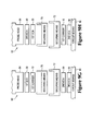
- Figure 11A shows the first carrier 10, the first ECA 30, the second ECA 80, the third ECA 90 and the fourth ECA 100 secured to the probe head 64 by the housing.
- the electrical contacts 96 exposed at one of the opposing surfaces 92, 94 of the third ECA 90 contact the electrical contacts on the circuit board in the probe head 64.
- the electrical contacts 106 exposed at one of the opposing surfaces 102, 104 of the fourth ECA 100 contact the electrical contacts on the circuit board 66 of the device under test when the probe head 64 is inserted into the socket housing 72 on the circuit board 66.
- the electrical contacts 36 exposed at one of the opposing surfaces 32, 34 of the first ECA 30 contact corresponding electrical contacts 96 exposed at the other of the opposing surfaces 92, 94 of the third ECA 90.
- the electrical contacts 36 exposed at the other of the opposing surfaces 32, 34 of the first ECA 30 contact corresponding electrical contacts 20 exposed at one of the opposing surfaces 12, 14 of the first carrier 10.
- the electrical contacts 20 exposed at the other of the opposing surfaces 12, 14 of the first carrier 10 contact corresponding electrical contacts 86 exposed at one of the opposing surfaces 82, 84 of the second ECA 80.
- the electrical contacts 86 exposed at the other of the opposing surfaces 82, 84 of the second ECA 80 contact corresponding electrical contacts 106 exposed at the other of the opposing surfaces 102, 104 of the fourth ECA 100.
- Figure 11B shows the first carrier 10, the first ECA 30, the second ECA 80, the third ECA 90 and the fourth ECA 100 secured to the circuit board 66 of the device under test by the socket housing 72.
- the electrical contacts 96 exposed at one of the opposing surfaces 92, 94 of the third ECA 90 contact the electrical contacts on the circuit board in the probe head 64 when the probe head 64 is inserted into the socket housing 72 on the circuit board 66 of the device under test.
- the electrical contacts 106 exposed at one of the opposing surfaces 102, 104 of the fourth ECA 100 contact the electrical contacts on the circuit board 66 of the device under test.
- the electrical contacts 36 exposed at one of the opposing surfaces 32, 34 of the first ECA 30 contact corresponding electrical contacts 96 exposed at the other of the opposing surfaces 92, 94 of the third ECA 90.
- the electrical contacts 36 exposed at the other of the opposing surfaces 32, 34 of the first ECA 30 contact corresponding electrical contacts 20 exposed at one of the opposing surfaces 12, 14 of the first carrier 10.
- the electrical contacts 20 exposed at the other of the opposing surfaces 12, 14 of the first carrier 10 contact corresponding electrical contacts 86 exposed at one of the opposing surfaces 82, 84 of the second ECA 80.
- the electrical contacts 86 exposed at the other of the opposing surfaces 82, 84 of the second ECA 80 contact corresponding electrical contacts 106 exposed at the other of the opposing surfaces 102, 104 of the fourth ECA 100.
- Figure 11C shows the first carrier 10, the first ECA 30, the second ECA 80 and the third ECA 90 secured to the probe head 64 by the housing 70 and the second ECA 80 and the fourth ECA 100 secured to the circuit board 66 of the device under test by the socket housing 72.
- the electrical contacts 96 exposed at one of the opposing surfaces 92, 94 of the third ECA 90 contact the electrical contacts on the circuit board in the probe head 64.
- the electrical contacts 106 exposed at one of the opposing surfaces 102, 104 of the fourth ECA 100 contact the electrical contacts on the circuit board 66 of the device under test.
- the electrical contacts 36 exposed at one of the opposing surfaces 32, 34 of the first ECA 30 contact corresponding electrical contacts 96 exposed at the other of the opposing surfaces 92, 94 of the third ECA 90.
- the electrical contacts 36 exposed at the other of the opposing surfaces 32, 34 of the first ECA 30 contact corresponding electrical contacts 20 exposed at one of the opposing surfaces 12, 14 of the first carrier 10.
- the electrical contacts 20 exposed at the other of the opposing surfaces 12, 14 of the first carrier 10 contact corresponding electrical contacts 86 exposed at one of the opposing surfaces 82, 84 of the second ECA 80.
- the electrical contacts 86 exposed at the other of the opposing surfaces 82, 84 of the second ECA 80 contact corresponding electrical contacts 106 exposed at the other of the opposing surfaces 102, 104 of the fourth ECA 100 when the probe head 64 is inserted into the socket housing 72 on the circuit board 66 of the device under test.
- Figure 11D shows the carrier 10, the first ECA 30 and the third EA90 secured to the probe head 64 by the housing 70 and the second ECA 80 and the fourth ECA 100 secured to the circuit board 66 of the device under test by the socket housing 72.
- the electrical contacts 96 exposed at one of the opposing surfaces 92, 94 of the third ECA 90 contact the electrical contacts on the circuit board in the probe head 64.
- the electrical contacts 106 exposed at one of the opposing surfaces 102, 104 of the fourth ECA 100 contact the electrical contacts on the circuit board 66 of the device under test.
- the electrical contacts 36 exposed at one of the opposing surfaces 32, 34 of the first ECA 30 contact corresponding electrical contacts 96 exposed at the other of the opposing surfaces 92, 94 of the third ECA 90.
- the electrical contacts 36 exposed at the other of the opposing surfaces 32, 34 of the first ECA 30 contact corresponding electrical contacts 20 exposed at one of the opposing surfaces 12, 14 of the first carrier 10.
- the electrical contacts 20 exposed at the other of the opposing surfaces 12, 14 of the first carrier 10 contact corresponding electrical contacts 86 exposed at one of the opposing surfaces 82, 84 of the second ECA 80 when the probe head 64 is inserted into the socket housing 72 on the circuit board 66 of the device under test.
- the electrical contacts 86 exposed at the other of the opposing surfaces 82, 84 of the second ECA 80 contact corresponding electrical contacts 106 exposed at the other of the opposing surfaces 102, 104 of the fourth ECA 100.
- FIG 11E shows the first ECA 30 and the third ECA 90 secured to the probe head 64 by the housing and the first carrier 10, second ECA 80 and the fourth ECA 100 secured to the circuit board 66 of the device under test by the socket housing 72.
- the electrical contacts 96 exposed at one of the opposing surfaces 92, 94 of the third ECA 90 contact the electrical contacts on the circuit board in the probe head 64.
- the electrical contacts 106 exposed at one of the opposing surfaces 102, 104 of the fourth ECA 100 contact the electrical contacts on the circuit board 66 of the device under test.
- the electrical contacts 36 exposed at one of the opposing surfaces 32, 34 of the first ECA 30 contact corresponding electrical contacts 96 exposed at the other of the opposing surfaces 92, 94 of the third ECA 90.
- the electrical contacts 36 exposed at the other of the opposing surfaces 32, 34 of the first ECA 30 contact corresponding electrical contacts 20 exposed at one of the opposing surfaces 12, 14 of the first carrier 10 when the probe head 64 is inserted into the socket housing 72 on the circuit board 66 of the device under test.
- the electrical contacts 20 exposed at the other of the opposing surfaces 12, 14 of the first carrier 10 contact corresponding electrical contacts 86 exposed at one of the opposing surfaces 82, 84 of the second ECA 80.
- the electrical contacts 86 exposed at the other of the opposing surfaces 82, 84 of the second ECA 80 contact corresponding electrical contacts 106 exposed at the other of the opposing surfaces 102, 104 of the fourth ECA 100.
- FIG 11F shows the third ECA 90 secured to the probe head 64 by the housing 70 and the first carrier 10, first ECA 30, second ECA 80 and the fourth ECA 100 secured to the circuit board 66 of the device under test by the socket housing 72.
- the electrical contacts 96 exposed at one of the opposing surfaces 92, 94 of the third ECA 90 contact the electrical contacts on the circuit board in the probe head 64.
- the electrical contacts 106 exposed at one of the opposing surfaces 102, 104 of the fourth ECA 100 contact the electrical contacts on the circuit board 66 of the device under test.
- the electrical contacts 36 exposed at one of the opposing surfaces 32, 34 of the first ECA 30 contact corresponding electrical contacts 96 exposed at the other of the opposing surfaces 92, 94 of the third ECA 90 when the probe head 64 is inserted into the socket housing 72 on the circuit board 66 of the device under test.
- the electrical contacts 36 exposed at the other of the opposing surfaces 32, 34 of the first ECA 30 contact corresponding electrical contacts 20 exposed at one of the opposing surfaces 12, 14 of the first carrier.
- the electrical contacts 20 exposed at the other of the opposing surfaces 12, 14 of the first carrier 10 contact corresponding electrical contacts 86 exposed at one of the opposing surfaces 82, 84 of the second ECA 80.
- the electrical contacts 86 exposed at the other of the opposing surfaces 82, 84 of the second ECA 80 contact corresponding electrical contacts 106 exposed at the other of the opposing surfaces 102, 104 of the fourth ECA 100.
- FIG. 3A and 3B The various configurations of the resistive probing tip system 62 according to the present invention are shown and described in Figures 3A and 3B , Figures 5A through 5G , Figures 6A through 6C , Figures 7A through 7L , Figures 8A through 8C , Figures 9A through 9J , Figures 10A through 10C and 11A through 11F using a first carrier 10.
- the configurations of Figures 6A through 6C , Figures 7A through 7L , Figures 8A through 8C , Figures 9A through 9J , Figures 10A through 10C and 11A through 11F may also be implemented using the first and second carriers 50, 52 as shown and described in relation to Figure 4 and Figures 5G through 5L without departing from the scope of the appended claims.
- numbered electrical contact assemblies i.e. first ECA 30, second ECA 80, third ECA 90, fourth ECA 100
- any one of the numbered electrical contact assemblies may be substituted in a position for any other of the numbered electrical contact assemblies without departing from the scope of the appended claims.
- Fig. 12 illustrates a sectional view of a first example of a logic analyzer probing system 200 using the resistive probing tip system 62 of the present invention.
- the logic analyzer probe head 64 has a substantially rectangular shaped body 202 having at least a first circuit board 204 with downward facing electrical contacts 206 formed on an edge surface thereof. Bores are formed within the body 202 adjacent to the side surfaces 208, 210 thereof that receive respective screws 212.
- the screws 212 have threaded end portions 214 the engage corresponding threaded bores (as shown in Figure 13 ) formed in the socket housing 72.
- the logic analyzer probe head 64 is positioned in the socket housing 72 with the screws 212 in the probe head 64 engaging the threaded bores in the socket housing 72. The tightening of the screws 212 in the threaded bores of the socket housing 72 secures the probe head 64 to the socket housing 72.
- the carrier 10 is shown with apertures 16 receiving the discrete resistors 18.
- the electrical contacts 20 on one end of each of the discrete resistors 18 exposed at the bottom surface 14 of the carrier 10 are positioned directly on one of the electrical contacts 216 on the circuit board 66 of the device under test.
- the electrical contacts 20 on the other end of the discrete resistors 18 exposed at the upper surface 12 of the carrier 10 mate with the electrical contacts 86 exposed at the bottom surface 84 of the second ECA 80.
- the electrical contacts 86 exposed at the top surface 82 of the second ECA 80 mate with the electrical contacts 36 exposed at the bottom surface 34 of the first ECA 30.
- the electrical contacts 36 exposed at the top surface 32 of the first ECA 30 mate with the electrical contacts 206 on the circuit board 204 of the probe head 64 when the probe head 64 is secured to the socket housing 72.
- the first ECA 30 is integrated in the socket housing 72 that secures the carrier 10 and second ECA 80 to the circuit board 66 of the device under test.
- the electrical contacts 36 of the first ECA 30 may be traditional C-shaped electrical contacts having a length of 0.10 inches. Since the stub length is minimized by the electrical contacts 20 of the discrete resistors 18 being in contact with the electrical contacts on the circuit board 66 of the device under test, the electrical contacts 36 can be optimized for their mechanical characteristics instead of being limited by stub length concerns.
- the socket housing 72 has downward extending metal pins 220 that are received in corresponding apertures 222 formed in the circuit board 66 of the device under test.
- the carrier 10 and the second ECA 80 have apertures 224 formed therein (as shown in Figure 13 ) that match the locations of the metal pins 220.
- the apertures 224 formed in the carrier 10 and the second ECA 80 are aligned with the metal pins 220 of the socket housing 72 and the apertures 222 formed in the circuit board 66 so that the carrier 10 and the second ECA 80 are captured between the socket housing 72 and the circuit board 66 when the socket housing 72 is positioned on the circuit board 66.
- the metal pins 220 of the socket housing 72 extend past the bottom surface 226 of the circuit board 66 of the device under test where solder or other types of affixing material 228 are used to secure the socket housing 72 to the circuit board 66 of the device under test.
- Figure 13 is an exploded perspective view showing a second example of a logic analyzer probing system 200 using the resistive probing tip system 62 of the present invention.
- the threaded portions 214 of screws 212 in the probe body 202 of the logic analyzer probe head 64 engage corresponding threaded bores 230 formed in the socket housing 72 for securing the probe head 64 to the socket housing 72.
- the socket housing 72 has metal pins 220 that are used to align the resistive probing tip system 62 in the logic analyzer probing system 200.
- the resistive probing tip system 62 in this example has a carrier 10 with apertures 16 formed therein that receive the discrete resistors 18.
- the electrical contacts 20 exposed the opposing ends of each of the discrete resistors 18 extend past the opposing surfaces 12, 14 of the carrier 10.
- the electrical contacts 20 on one end of the discrete resistors 18 contact the electrical contacts 36 exposed at the bottom surface 34 of the first ECA 30.
- the electrical contacts 20 on the other end of the discrete resistors 18 contact the electrical contacts 86 exposed at the top surface 82 of the second ECA 80.
- the electrical contacts 86 exposed at the bottom surface 84 of the second ECA 80 contact the electrical contacts on the circuit board 66 of the device under test.
- the socket housing 72 may include a third ECA 90 having electrical contacts 96, such as C-shaped electrical contacts or the like, that contact the electrical contacts 36 exposed at the top surface 32 of the first ECA 30.
- the electrical contacts 96 in the socket housing 72 contact the electrical contacts 206 exposed at the bottom edge of the circuit board 204 in the logic analyzer probe head 64.
- FIG 14 is an exploded perspective view showing third example of a logic analyzer probing system 200 using the resistive probing tip system 62 of the present invention.
- the first ECA 30 is disposed in the socket housing 72.
- the upward facing electrical contacts 36 shown in the socket housing 72 contact the electrical contacts 206 exposed at the bottom edge of the circuit board 204 in the logic analyzer probe head 64 when the probe head 64 is inserted into the socket housing 72.
- the bottom facing electrical contacts 36 in the socket housing 72 contact the electrical contacts 20 exposed at the upper surface 12 of the carrier 10.
- the electrical contacts 20 exposed at the bottom surface 14 of the carrier 10 contact the electrical contacts 86 exposed at the upper surface 82 of the second ECA 80.
- the electrical contacts 86 exposed at the bottom surface 84 of the second ECA 80 contact the electrical contacts exposed on the circuit board 66 of the device under test.
- FIG 15 is an exploded perspective view showing a fourth example of a logic analyzer probing system 200 using the resistive probing tip system 62 of the present invention.
- first and second carriers 50 and 52 such as described with respect to Figure 4 , that mate with first and second circuit boards 240 and 242 disposed in the body 202 probe head 64.
- Bores are formed within the body 202 adjacent to the side surfaces 208, 210 thereof that receive respective screws 212.
- the screws 212 have threaded end portions 214 the engage corresponding threaded bores 230 formed in the socket housing 72.
- the logic analyzer probe head 64 is positioned in the socket housing 72 with the screws 208 in the probe head 64 engaging the threaded bores in the socket housing 72. The tightening of the screws 208 in the threaded bores of the socket housing 72 secures the probe head 64 to the socket housing 72.
- a first ECA 30, such as described with respect to Figure 3B has electrical contacts 36 exposed at the top surface 32 that contact downward facing electrical contacts 206 formed on the edge surfaces of the circuit boards 240, 242.
- the electrical contacts 36 exposed at the bottom surface 34 of the first ECA contact the respective electrical contacts 56 exposed at the top edge surfaces 58 of the first and second carriers 50 and 52.
- the first ECA 30 and the first and second carriers 50, 52 are secured to the probe head 64 by housing 70.
- the housing 70 has lateral slots 244 formed therein with inward extending shouldered ribs 246 which support the first and second carriers 50, 52 in the lateral slots 244.
- the electrical contacts 56 exposed at the bottom edge surfaces 58 of the first and second carriers 50, 52 are exposed in the lateral slots 244.
- a second ECA 80 is formed from elastomeric material having multiple elements 248.
- Each of the elastomeric elements 248 has electrical contacts 86 formed through the elastomeric material.
- the electrical contacts 86 may be formed from multiple fine electrical wires with the fine electrical wires extending to the opposing surfaces 82, 84 of the multiple elastomeric elements 248 in the second ECA 80.
- the multiple elastomeric elements 248 of the second ECA 80 are positioned in slots 250 formed in the socket housing 72.
- the socket housing 72 is secured to the circuit board 66 of the device under test using the metal pins 220 such that the electrical contacts 86 exposed at the bottom surface 84 of the multiple elastomeric elements 248 contact the electrical contacts on the circuit board 66 of the device under test.
- the electrical contacts 86 exposed at the top surface 82 of the multiple elastomeric elements 248 contact corresponding electrical contacts 56 exposed at the bottom edge surfaces of the first and second carriers 50, 52 when the probe head 64 is inserted into the
- Figure 16 is an exploded perspective view showing another example of a logic analyzer probing system 200 using the resistive probing tip system 62 of the present invention.
- the electrical contact assembly between the circuit boards 240, 242 in the probe head 64 and the first and second carriers 50 and 52, as shown in Figure 15 is removed.
- the electrical contacts 56 exposed at the upper edge surfaces 58 of the first and second carriers 50, 52 respectively contact corresponding electrical contacts exposed at the bottom edges of the first and second circuit boards 240, 242.
- the electrical contacts56 exposed at the bottom edge surfaces of the first and second carriers 50, 52 contact the electrical contacts 36 exposed at the top surfaces 32 of the multiple elastomeric elements 248 of the first ECA 30 when the probe head is inserted in the socket housing 72.
- the electrical contacts 36 exposed at the bottom surface 34 of the multiple elastomeric elements 248 contact the electrical contacts on the circuit board 66 of the device under test.
- Some of the configurations of the resistive probing tip system 62 have two electrical contact assemblies between the electrical contacts on the circuit board 66 of the device under test and the carrier or carriers 10, 50, 52.
- the electrical contact assemblies have various heights depending on the materials used.
- An electrical contact assembly made of flex circuit material has a nominal height of 0.010 inches.
- An electrical contact assembly made of elastomeric material has a nominal free height of 0.039 inches and a nominal compressed height of 0.031 inches.
- An electrical contact assembly having metal spring electrical contacts disposed in a housing has a nominal free height of 0.036 inches and a nominal compressed height of 0.031 inches.
- Two electrical contact assemblies made of flex circuit material have a nominal height of 0.020 inches.
- a combination of a first electrical contact assembly made with flex circuit material and a second electrical contact assembly made elastomeric material or made with metal spring electrical contacts in a housing have a nominal compressed height of 0.041 1 inches.
- Two electrical contact assemblies made from either of the elastomeric material or metal spring electrical contacts disposed in a housing have a nominal compressed height of 0.062 inches.
- a logic analyzer probing system 200 of Figure 15 constructed with resistive probing tip system 62 has successfully probed device under test circuitry operating at 8 Gb/s.
- prior art logic analyzer probing systems are unable to probe device under test circuitry operating faster than 5 Gb/s. Additional increases in the speed of device under test circuitry that can be successfully probed by a logic analyzer probing system 200 constructed with the resistive probing tip system 62 are likely if the size of the discrete resistive elements 18 are reduced.
- the current resistive elements 18 of carrier 10 are comparable in size to 0402 discrete resistors. This finding indicates that a logic analyzer probing system 200 constructed with 0402 discrete resistor elements 18 can also successfully probe DUT circuits operating at 8 Gb/s.
- the logic analyzer probing system constructed with resistive elements made with 0201 discrete resistors should be able to successfully probe DUT circuits operating significantly faster than 8 Gb/s.
Landscapes
- Engineering & Computer Science (AREA)
- Microelectronics & Electronic Packaging (AREA)
- Physics & Mathematics (AREA)
- General Physics & Mathematics (AREA)
- Measuring Leads Or Probes (AREA)
Abstract
Description
- The present invention relates to resistive probing tip systems, and more particularly to resistive probing tip systems incorporated into logic analyzer probing systems for highspeed probing of a device under test.
- One of the problems with making a high speed logic analyzer probe is that the probe will perturb the system under test. These types of probes generally have input impedances of a few hundred ohms, but there is usually a short compliant contact between the electrical contact on the circuit board of the device under test (DUT) and the input resistance, which is described in
U.S. Patents 6,888,361 and6,781,391 , which are incorporated herein by reference. In multi-conductor probing applications involving logic analyzer probes or Mixed Signal Oscilloscope probes, an interconnect is employed to achieve individual compliance of each contact being tested, resulting in a stub. - A prime example is a probe head with pogo pins. These provide adequate compliance, but become an unterminated stub on the circuit being tested. This unterminated stub will reflect energy back into the system under test, so a long time delay in the compliant contact is undesirable. Electrical stubs can impact the circuit being probed, so probe designers seek to minimize the stubs. The ideal probe tip would have a resistive element at the point of contact, thereby creating no stub.
- However, existing probing methods place input resistors approximately 0.100 inches from the DUT contact points of the circuit to be probed, creating a 'stub' on the probed circuit. Two elements contribute to the 'stub length': (1) the compliant interconnect socket, and (2) limitations of placing resistors close to the edge of the circuit board of the probe head. The length of the time delay in the compliant contact is one of the factors that limit the speed at which the probe can be used.
- An example of a compliant interconnect socket is a SpiritⓇ Compression Test Probe, manufactured and sold by Samtec, Inc., New Albany, Indiana. The SpiritⓇ Compression Test Probe has mounting brackets positioned on either side of parallel rows of contact points on a circuit board of the DUT. Parallel rows of passive resistors corresponding to the parallel rows of contact points on the circuit board are embedded in a connector housing that is positioned between the mounting brackets. Each passive resistor is secured to a lower spring contact and an upper spring contact with the lower spring contact engaging one of the contact points on the circuit board and the upper spring contact engaging a corresponding contact point in a probe head. The stub length of the lower spring contact is 0.100 inches.
- In previous implementations of logic analyzer probes, the resistor has resided on a circuit board in the probe head, and the compliant contact comes into contact with the edge of the circuit board. The length of the contact and the amount the resistor is set back from the edge of the circuit board both contribute to the unterminated stub length. The distance that the resistor is set back from the edge of the circuit board is determined by circuit board manufacturing constraints. In addition, the edge wrap on the circuit board produces an edge that is somewhat rough and departs from planarity because of the process of routing and plating the laminated circuit board edge. Therefore, there is a need for a resistive probing tip system that enables probing at higher speeds by decreasing the stub length on the probed circuit.
- The present invention provides a resistive probing tip system usable in a logic analyzer probing system that overcomes the above-mentioned disadvantages and drawbacks of the prior art. The resistive probing tip system has at least a first carrier and a first electrical contact assembly. The first carrier has opposing surfaces with a plurality of resistors engaging the first carrier. Each of the plurality of resistors has opposing electrical contacts that are exposed at respective surfaces of the first carrier. The plurality of resistors may be discrete resistors disposed in apertures formed through the first carrier. The first carrier may also be a ceramic substrate with the plurality of resistors disposed one or both of the opposing surfaces of the substrate. The first electrical contact assembly has opposing surfaces with electrical contacts exposed at the respective opposing surfaces. Each electrical contact exposed at one opposing surface is electrically coupled to a corresponding electrical contact exposed at the other opposing surface. The first electrical contact assembly may be formed using flex circuit material or formed using an elastomeric material having electrically conductive elastomeric contact. The first electrical contact assembly may also be formed using a housing having compressible spring contacts disposed therein. The first carrier and the first electrical contact assembly selectively mate to and mate from each other with the electrical contacts exposed at one surface of the first carrier and the electrical contacts exposed at one surface of the first electrical contact assembly contacting each other. The first carrier and/or the first electrical contact assembly may be selectively secured to either of a circuit board of a device under test or a probe head.
- The resistive probing tip system may also have multiple carriers having opposing surfaces. The multiple carriers have the same or similar construction as the first carrier. The first carrier and one or more of the multiple carriers selectively mate to and mate from the first electrical contact assembly. The electrical contacts exposed at one surface of the respective first carrier and one or more of the multiple carriers contact corresponding electrical contacts exposed at one surface of the first electrical contact assembly. The first carrier and one or more of the multiple carriers and/or the first electrical contact assembly may be selectively secured to either of a circuit board of a device under test or a probe head.
- The resistive probing tip system may also have multiple electrical contact assemblies having opposing surfaces. The multiple electrical contact assemblies have the same or similar construction as the first electrical contact assembly. The electrical contacts exposed at the opposing surfaces of the first electrical contact assembly, one or more of the multiple electrical contact assemblies, the first carrier and one or more of the multiple carriers selectively contact corresponding electrical contacts exposed at the mating opposing surfaces of the first electrical contact assembly, one or more of the multiple electrical contact assemblies, the first carrier and one or more of the multiple carriers. The first carrier or the first carrier and one or more of the multiple carriers and/or the first electrical contact assembly and/or the first electrical contact assembly and one or more of the multiple electrical contact assemblies may be selectively secured to either of a circuit board of a device under test or a probe head.
- The resistive probing tip system may be configured with the first carrier or the first and one or more of the multiple carriers disposed between the first electrical contact assembly and a second electrical contact assembly of the multiple electrical contact assemblies. A third electrical contact assembly of the multiple electrical contact assemblies may be included that selectively mates to and mates from at least one of the first electrical contact assembly and the second electrical contact assembly. A fourth electrical contact assembly of the multiple electrical contact assemblies may be included that selectively mates to and mates from the other of the first electrical contact assembly and the second electrical contact assembly.
- A logic analyzer probing system has a probe head containing at least a first circuit board having electrical contacts thereon and a resistive probing tip system having at least a first carrier and a first electrical contact assembly. The first carrier has opposing surfaces with a plurality of resistors engaging the first carrier. Each of the plurality of resistors has opposing electrical contacts that are exposed at respective surfaces of the first carrier. The plurality of resistors may be discrete resistors disposed in apertures formed through the first carrier. The first carrier may also be a ceramic substrate with the plurality of resistors disposed one or both of the opposing surfaces of the substrate. The first electrical contact assembly has opposing surfaces with electrical contacts exposed at the respective opposing surfaces. Each electrical contact exposed at one opposing surface is electrically coupled to a corresponding electrical contact exposed at the other opposing surface. The first electrical contact assembly may be formed using flex circuit material or formed using an elastomeric material having electrically conductive elastomeric contact. The first electrical contact assembly may also be formed using a housing having compressible spring contacts disposed therein. The first circuit board, the first electrical contact assembly and the first carrier selectively mate to and mate from one another with the electrical contacts exposed at the surfaces of the first circuit board, the first electrical contact assembly and the first carrier contacting corresponding electrical contacts exposed at the mating surfaces of the first circuit board of the probe head, the first electrical contact assembly and the first carrier. A housing secures at least one of the first electrical contact assembly and the first carrier between the first circuit board of the probe head and the housing.
- The logic analyzer probing system may also have at least a second electrical contact assembly having opposing surfaces. The second electrical contact assembly has the same or similar construction as the first electrical contact assembly. The first electrical contact assembly, second electrical contact assembly and the first carrier selectively mate to and mate from one another with the electrical contacts exposed at the opposing surfaces of the first electrical contact assembly, the second electrical contact assembly and the first carrier contacting corresponding electrical contacts exposed at the mating surfaces of the first electrical contact assembly, the second electrical contact assembly and the first carrier. The housing receives the second electrical contact assembly or the first carrier for capturing the first carrier, the first electrical contact assembly and the second electrical contact assembly or the first electrical contact assembly and the second electrical contact assembly between the first circuit board of the probe head and the housing.
- The second electrical contact assembly may also be secured to a circuit board of a device under test having a plurality of electrical contacts. The electrical contacts exposed at one surface of the second electrical contact assembly selectively mates to and mates from the electrical contacts of the circuit board of the device under test and the electrical contacts exposed at the other surface of the second electrical contact assembly selectively mate to and mate from the electrical contacts of the first carrier or the first electrical contact assembly.
- The probe head of the logic analyzer probing system may also have a second circuit board having electrical contacts thereon and a second carrier. The second carrier has the same or similar construction as the first carrier. The second circuit board of the probe head, the first electrical contact assembly and the second carrier selectively mate to and mate from one another with the electrical contacts exposed the surfaces of the second circuit board of the probe head, the first electrical contact assembly and the second carrier contacting corresponding electrical contacts exposed at the mating surfaces of the second circuit board of the probe head, the first electrical contact assembly and the second carrier. The housing receives the first electrical contact assembly or the first and second carriers for capturing the first electrical contact assembly and the first and second carriers or the first electrical contact assembly or the first and second carriers between the first and second circuit boards of the probe head and the housing.
- A second electrical contact assembly may also be used with a second circuit board in the probe head having electrical contacts thereon and a second electrical contact assembly. The second electrical contact assembly has the same or similar construction as the first electrical contact assembly. The second electrical contact assembly selectively mates to and mates from the first and second carriers or the first electrical contact assembly with the electrical contacts exposed at the surfaces of the second electrical contact assembly contacting corresponding electrical contacts exposed at the mating surfaces of the first and second carriers or the first electrical contact assembly. The housing receives the second electrical contact assembly or the first and second carriers for capturing the first and second carriers, the first electrical contact assembly and the second electrical contact assembly or the first electrical contact assembly and the second electrical contact assembly between the first and second circuit boards of the probe head and the housing.
- The second electrical contact assembly may also be secured to a circuit board of a device under test having a plurality of electrical contacts. The electrical contacts exposed at one surface of the second electrical contact assembly selectively mates to and mates from the electrical contacts of the circuit board of the device under test and the electrical contacts exposed at the other surface of the second electrical contact assembly selectively mate to and mate from the electrical contacts of the first and second carriers or the first electrical contact assembly.
- The objects, advantages and other novel features of the present invention are apparent from the following detailed description when read in conjunction with the appended claims and attached drawings.
-
Figure 1 is an exploded perspective view of a first embodiment of a carrier receiving discrete resistive elements usable in a resistive probing tip system according to the present invention. -
Figures 2A and2B are perspective views of a second embodiment of a carrier having resistive elements and electrical contacts formed thereon usable in a resistive probing tip system according to the present invention. -
Figure 3A is an exploded perspective view of a first embodiment of an electrical contact assembly usable in a resistive probing tip system according to the present invention. -
Figure 3B is a perspective view of a second embodiment of an electrical contact assembly usable in a resistive probing tip system according to the present invention. -
Figure 4 an exploded perspective view of an electrical contact assembly and first and second carriers usable in a resistive probing tip system according to the present invention. -
Figures 5A through 5L are various configurations using an electrical contact assembly and first or first and second carriers and in the resistive probing tip system according to the present invention. -
Figure 6A through 6C are exploded perspective views of a carrier and first and second electrical contact assemblies usable in a resistive probing tip system according to the present invention. -
Figures 7A through 7L are various configurations using first and second electrical contact assemblies and a carrier in the resistive probing tip system according to the present invention. -
Figure 8A through 8C are exploded perspective views of a carrier and first, second and third electrical contact assemblies usable in a resistive probing tip system according to the present invention. -
Figures 9A through 9J are various configurations using first, second and third electrical contact assemblies and a carrier in the resistive probing tip system according to the present invention. -
Figure 10A through 10C are exploded perspective views of a carrier and first, second, third and fourth electrical contact assemblies usable in a resistive probing tip system according to the present invention. -
Figures 11A through 11F are various configurations using first, second, third and fourth electrical contact assemblies and a carrier in the resistive probing tip system according to the present invention. -
Figure 12 is a first example of a logic analyzer probing system using the resistive probing tip system of the present invention. -
Figure 13 is a second example of a logic analyzer probing system using the resistive probing tip system of the present invention. -
Figure 14 is a third example of a logic analyzer probing system using the resistive probing tip system of the present invention. -
Figure 15 is a fourth example of a logic analyzer probing system using the resistive probing tip system of the present invention. -
Figure 16 is another example of a logic analyzer probing system using the resistive probing tip system of the present invention. - Referring to
Figure 1 , there is shown an exploded perspective view of acarrier 10 usable in a resistive probing tip system according to the present invention. Thecarrier 10 may be formed as a planar body having opposingsurfaces Apertures 16 are formed through thecarrier 10 that extend to the opposingsurfaces resistive elements 18 havingelectrical contacts 20 at opposing ends thereof are disposed in theapertures 16 with theelectrical contacts 20 of the discreteresistive elements 18 exposed at the opposingsurfaces carrier 10. Discreteresistive elements 18 that are suitable for use incarrier 10 include the CRCW0402 and CRCW0201 Thick Film, Rectangular Chip Resistors, manufactured and sold by Vishay Intertechnolgy, Inc., Malvern, Pennsylvania. Acarrier 10 formed of elastomer preferably should have a durometer of approximately 70 (Shore A) in the current embodiment in order to both retain theresistive elements 18 and permit individual compliance of eachresistive element 18. However, a durometer ranging from approximately 50 to approximately 100 would also be suitable. -
Figures 2A and2B shows perspective top and bottom views of anothercarrier 10 that may be formed as a substrate using a ceramic material or the like. Theceramic substrate carrier 10 has opposingsurfaces electrical contacts 20 formed on the opposingsurfaces Resistive elements 22 are formed on theceramic substrate carrier 10 with each end of theresistive elements 22 being coupled to anelectrical contact 20. Theresistive elements 22 andelectrical contacts 20 are formed using well-known thick film, thin film, or other technologies. One of theelectrical contacts 20 of eachresistive element 22 is formed on one of the opposingsurfaces ceramic substrate carrier 10 and the otherelectrical contact 20 of eachresistive element 22 is formed on the other of the opposingsurface ceramic substrate carrier 10. Alternately, theelectrical contacts 20 may be formed on the opposing side surfaces of theceramic substrate carrier 10 with this alternative being equivalent to theelectrical contacts 20 being formed on the opposingflat surfaces ceramic substrate carrier 10. A further alternative has theresistive elements 22 formed of discrete resistors with one end of each discrete resistor connected to anelectrical contact 20 formed on one of the opposing side surfaces of theceramic substrate carrier 10 and the other end of each discrete resistor connected to anelectrical contact 20 formed on the other of the side surfaces of theceramic substrate carrier 10. - The resistive probing tip system according to the present invention has at least a first electrical contact assembly (first ECA) 30 as shown in
Figures 3A and3B . Theelectrical contact assembly 30 has opposingsurfaces electrical contacts 36 exposed at the opposingsurfaces electrical contact 36 exposed at one of the opposingsurfaces electrical contact 36 exposed at the other opposing surface. Theelectrical contacts 36 exposed at the opposingsurfaces electrical contacts 20 of theresistive elements surfaces carrier 10. In one embodiment, theelectrical contact assembly 30 is formed of aflex circuit material 38 having correspondingelectrical contacts 36 formed on the opposingsurfaces flex circuit material 38 has a thickness on the order of 0.010 inches. In a second embodiment, the electrical contact assembly may be formed of an elastomeric material having electrically conductive contacts formed through the elastomeric material. In one design, multiple fine electrical wires form each of the electrical contacts with the fine electrical wires extending to the opposingsurfaces electrical contact assembly 30. Preferably, the elastomeric material has a free height on the order of 0.039 inches and a compressed height of 0.031 inches.Figure 3B show a further embodiment of theelectrical contact assembly 30 where metal springelectrical contacts 36 are disposed in ahousing 40 with the ends of the metal spring electrical contacts extending fromapertures 42 formed in the opposingsurfaces electrical contact assembly 30. An example of a metal spring electrical contacts usable in theelectrical contact assembly 30 are RC Spring Probes manufactured and sold by Ardent Concepts, Inc., Hampton Beach, New Hampshire. Preferably, the free height of the metal spring electrical contact is 0.036 inches. The compressed height is 0.031 inches which is set by the thickness of thehousing 40 of theelectrical contact assembly 30. -
Figure 4 show an alternative embodiment for the resistive probing tip system according to the present invention. The embodiment ofFigure 4 has first andsecond carriers carriers resistive elements 54 formed thereon.Electrical contacts 56 are formed on the ends of theresistive elements 54 with theelectrical contacts 56 extending over the opposing side surfaces 58 and 60 of theceramic substrate carriers resistive elements 54 andelectrical contacts 56 are formed using well-known thick film, thin film, or other technologies. In an alternate embodiment, theresistive elements 54 may be discrete resistors having opposingelectrical contact 56 that are secured to acarrier electrical contacts 56 of thediscrete resistors 54 extend above opposing surfaces of the circuit board. - Referring to
Figures 5A-5L , there are shown various configurations of the resistive probingtip system 62 according to the present invention. The carrier orcarriers first ECA 30 may be secured to aprobe head 64 of a logic analyzer probe or secured to acircuit board 66 of a device under test. Theprobe head 64 has at least a first circuit board (not shown) having electrical contacts corresponding to theresistive elements carriers electrical contacts surfaces carriers electrical contacts 36 exposed at one of the opposingsurfaces first ECA 30. Theelectrical contacts surface carriers electrical contacts 36 exposed at the other of the opposingsurfaces first ECA 30 selectively mate to and mate from the electrical contacts on the circuit board of theprobe head 64. Likewise, theelectrical contacts surface carriers electrical contacts 36 exposed at the other of the opposingsurfaces first ECA 30 selectively mate to and mate from the electrical contacts on thecircuit board 66 of the device under test. The capability of thecarrier 10 orcarriers first ECA 30 to selectively mate to and mate with one another and mate to and mate from the circuit board of theprobe head 64 and/or thecircuit board 66 of the device under test allows the selective replacement of the carrier or carriers and electrical contact assembly to be selectively replaced if one of them becomes inoperative. - In
Figure 5A , thefirst carrier 10 and thefirst ECA 30 are secured to theprobe head 64 by ahousing 70 mating with theprobe head 64. Theelectrical contacts 20 exposed at one of the opposingsurfaces first carrier 10 contact the electrical contacts on the circuit board in theprobe head 64. Theelectrical contacts 36 exposed at one of the opposingsurfaces first ECA 30 contact the electrical contacts on thecircuit board 66 of the device under test when theprobe head 64 is secured to thecircuit board 66 of the device under test using a securing means, such as a logicprobe socket housing 72. Theelectrical contacts 20 exposed at the other of the opposingsurfaces first carrier 10 contact correspondingelectrical contacts 36 exposed at the other of the opposingsurfaces first ECA 30. - In
Figure 5B , the positions of thefirst carrier 10 and thefirst ECA 30 are reversed. Theelectrical contacts 36 exposed at one of the opposingsurfaces first ECA 30 contact the electrical contacts on the circuit board in theprobe head 64. Theelectrical contacts 20 exposed at one of the opposingsurfaces first carrier 10 contact the electrical contacts on thecircuit board 66 of the device under test when theprobe head 64 is inserted into thesocket housing 72 on thecircuit board 66. Theelectrical contacts 36 exposed at the other of the opposingsurfaces first ECA 30 contact correspondingelectrical contacts 20 exposed at the other of the opposingsurfaces first carrier 10. - In
Figure 5C , thefirst carrier 10 is secured to theprobe head 64 by thehousing 70 and thefirst ECA 30 is secured to thecircuit board 66 of the device under test by thesocket housing 72. Theelectrical contacts 20 exposed at one of the opposingsurfaces first carrier 10 contact the electrical contacts on the circuit board in theprobe head 64. Theelectrical contacts 36 exposed at one of the opposingsurfaces first ECA 30 contact the electrical contacts on thecircuit board 66 of the device under test. Theelectrical contacts 20 exposed at the other of the opposingsurfaces first carrier 10 contact correspondingelectrical contacts 36 exposed at the other of the opposingsurfaces first ECA 30 when theprobe head 64 is inserted into thesocket housing 72 on thecircuit board 66. - In
Figure 5D , thefirst ECA 30 is secured to theprobe head 64 by thehousing 70 and thefirst carrier 10 is secured to thecircuit board 66 of the device under test by thesocket housing 72. Theelectrical contacts 36 exposed at one of the opposingsurfaces first ECA 30 contact the electrical contacts on the circuit board in theprobe head 64. Theelectrical contacts 20 exposed at one of the opposingsurfaces first carrier 10 contact the electrical contacts on thecircuit board 66 of the device under test. Theelectrical contacts 36 exposed at the other of the opposingsurfaces first ECA 30 contact correspondingelectrical contacts 20 exposed at the other of the opposingsurfaces first carrier 10 when theprobe head 64 is inserted into thesocket housing 72 on thecircuit board 66. - In
Figure 5E , thefirst carrier 10 and thefirst ECA 30 are secured to thecircuit board 66 of the device under test by thesocket housing 72. Theelectrical contacts 20 exposed at one of the opposingsurfaces first carrier 10 contact theelectrical contacts 36 exposed at the one of the opposingsurfaces first ECA 30. Theelectrical contacts 36 exposed at the other of the opposingsurfaces first ECA 30 contact the electrical contacts on thecircuit board 66 of the device under test. Theelectrical contacts 20 exposed at the other of the opposingsurfaces first carrier 10 contact corresponding the electrical contacts on the circuit board in theprobe head 64 when theprobe head 64 is inserted into thesocket housing 72 on thecircuit board 66. - In
Figure 5F , the positions of thefirst carrier 10 and thefirst ECA 30 are reversed. Thefirst ECA 30 and thefirst carrier 10 are secured to thecircuit board 66 of the device under test by thesocket housing 72. Theelectrical contacts 36 exposed at one of the opposingsurfaces first ECA 30 contact theelectrical contacts 20 exposed at the one of the opposingsurfaces first carrier 10. Theelectrical contacts 20 exposed at the other of the opposingsurfaces first carrier 10 contact the electrical contacts on thecircuit board 66 of the device under test. Theelectrical contacts 36 exposed at the other of the opposingsurfaces first ECA 30 contact corresponding the electrical contacts on the circuit board in theprobe head 64 when theprobe head 64 is inserted into thesocket housing 72 on thecircuit board 66. - In
Figure 5G , first andsecond carriers first ECA 30 are secured to theprobe head 64 by thehousing 70 mating with theprobe head 64. Theelectrical contacts 56 exposed at one of the opposingsurfaces second carriers probe head 64. Theelectrical contacts 56 exposed at the other opposingsurfaces second carriers electrical contacts 36 on one of the opposingsurfaces first ECA 30. Theelectrical contacts 36 exposed at the other of opposingsurfaces first ECA 30 contact the electrical contacts on thecircuit board 66 of the device under test when theprobe head 64 is inserted into thesocket housing 72 on thecircuit board 66. As with the previous configurations, theprobe head 64 is mounted to thecircuit board 66 using a securing means, such as alogic probe socket 72. - In
Figure 5H , the positions of the first andsecond carriers first ECA 30 are reversed. Theelectrical contacts 36 exposed at one of the opposingsurfaces first ECA 30 contact the electrical contacts on the first and second circuit board in theprobe head 64. Theelectrical contacts 36 exposed at the other of the opposingsurfaces first ECA 30 contact correspondingelectrical contacts 56 exposed at the other of the opposingsurfaces second carriers electrical contacts 56 exposed at the other of the opposingsurfaces second carriers circuit board 66 of the device under test when theprobe head 64 is inserted into thesocket housing 72 on thecircuit board 66. - In
Figure 5I , the first andsecond carriers probe head 64 by thehousing 70 and thefirst ECA 30 is secured to thecircuit board 66 of the device under test by thesocket housing 72. Theelectrical contacts 56 exposed at one of the opposingsurfaces second carriers probe head 64. Theelectrical contacts 36 exposed at one of the opposingsurfaces first ECA 30 contact the electrical contacts on thecircuit board 66 of the device under test. Theelectrical contacts 56 exposed at the other of the opposingsurfaces second carriers electrical contacts 36 exposed at the other of the opposingsurfaces first ECA 30 when theprobe head 64 is inserted into thesocket housing 72 on thecircuit board 66. - In
Figure 5J , thefirst ECA 30 is secured to theprobe head 64 by thehousing 70 and the first andsecond carriers circuit board 66 of the device under test by thesocket housing 72. Theelectrical contacts 36 exposed at one of the opposingsurfaces first ECA 30 contact the electrical contacts on the first and second circuit board in theprobe head 64. Theelectrical contacts 56 exposed at one of the opposingsurfaces second carriers circuit board 66 of the device under test. Theelectrical contacts 36 exposed at the other of the opposingsurfaces first ECA 30 contact correspondingelectrical contacts 56 exposed at the other of the opposingsurfaces second carriers probe head 64 is inserted into thesocket housing 72 on thecircuit board 66. - In
Figure 5K , the first andsecond carriers first ECA 30 are secured to thecircuit board 66 of the device under test by thesocket housing 72. Theelectrical contacts 56 exposed at one of the opposingsurfaces second carriers electrical contacts 36 exposed at one of the opposingsurfaces first ECA 30. Theelectrical contacts 36 exposed at the other of the opposingsurfaces first ECA 30 contact the electrical contacts on thecircuit board 66 of the device under test. Theelectrical contacts 56 exposed at the other of the opposingsurfaces second carriers probe head 64 when theprobe head 64 is inserted into thesocket housing 72 on thecircuit board 66. - In
Figure 5L , thefirst ECA 30 and the first andsecond carriers circuit board 66 of the device under test by thesocket housing 72. Theelectrical contacts 36 exposed at one of the opposingsurfaces first ECA 30 contact correspondingelectrical contacts 56 exposed at one of the opposingsurfaces second carriers electrical contacts 56 exposed at the other of the opposingsurfaces second carriers circuit board 66 of the device under test. Theelectrical contacts 36 exposed at the other of the opposingsurfaces first ECA 30 contact the electrical contacts on the first and second circuit boards of theprobe head 64 when theprobe head 64 is inserted into thesocket housing 72 on thecircuit board 66. -
Figures 6A ,6B and6C show further configurations of the resistive probingtip system 62 according to the present invention.Figure 6A show thecarrier 10 ofFigure 1 disposed between thefirst ECA 30 and a second electrical contact assembly (second ECA) 80. Thecarrier 10 has opposingsurface discrete resistors 18 disposed inapertures 16 formed in thecarrier 10.Electrical contacts 20 formed on the opposing ends of thediscrete resistors 18 are exposed at the opposingsurfaces Figures 6B and6C show perspective top and bottom views of the previously describedceramic substrate carrier 10 disposed between thefirst ECA 30 and thesecond ECA 80. Theceramic substrate carrier 10 has opposingsurfaces electrical contacts 20 formed on the opposing surfaces.Resistive elements 22 are formed on theceramic substrate carrier 10 with eachresistive element 22 having one end connected to one of theelectrical contacts 20 on one of the opposingsurfaces resistive element 22 connected to one of theelectrical contacts 20 on the other opposingsurface ceramic substrate carrier 10. Thesecond ECA 80 has opposingsurfaces electrical contacts 86 being exposed at the opposingsurfaces electrical contact 86 exposed at one of the opposingsurfaces second ECA 80 is electrically coupled to a correspondingelectrical contact 86 exposed at the other opposingsurface second ECA 80 is formed in the same manner as previously described for thefirst ECA 30. - The
electrical contacts 20 exposed at the opposingsurfaces first carrier 10 selectively mate to and mate from theelectrical contacts 36 exposed at one of the opposingsurfaces first ECA 30 and theelectrical contacts 86 exposed at one of the opposingsurfaces second ECA 80. Theelectrical contacts 20 exposed at one of the opposingsurface carrier 10 or theelectrical contacts 36 exposed at one of the opposingsurfaces first ECA 30 selectively mate to and mate from the electrical contacts on the circuit board of theprobe head 64. Likewise, theelectrical contacts 20 exposed at one of the opposingsurface carrier 10 or theelectrical contacts 86 exposed at one of the opposingsurfaces second ECA 80 selectively mate to and mate from the electrical contacts on thecircuit board 66 of the device under test. -
Figures 7A-7L show various configurations of the resistive probingtip system 62 according to the present invention having thefirst ECA 30 andsecond ECA 80. In these configurations, thefirst carrier 10, thefirst ECA 30 and thesecond ECA 80 may be secured to theprobe head 64 of a logic analyzer probe or secured to thecircuit board 66 of a device under test. Further configurations include one of thefirst ECA 30 or thefirst carrier 10 being secured to theprobe head 64 of a logic analyzer probe or secured to thecircuit board 66 of a device under test. Also, thefirst carrier 10 or one of thefirst ECA 30 and thesecond ECA 80 may be secured to theprobe head 64 or to thecircuit board 66 of the device under test. - In
Figures 7A, 7B and 7C thefirst carrier 10, thefirst ECA 30 andsecond ECA 80 are secured to theprobe head 64 by thehousing 70 mating with theprobe head 64. InFigure 7A , theelectrical contacts 36 exposed at one of the opposingsurfaces first ECA 30 contact the electrical contacts on the circuit board in theprobe head 64. Theelectrical contacts 86 exposed at one of the opposingsurfaces second ECA 80 contact the electrical contacts on thecircuit board 66 of the device under test when theprobe head 64 is inserted into thesocket housing 72 on thecircuit board 66. Theelectrical contacts 20 exposed at one of the opposingsurfaces first carrier 10 contact correspondingelectrical contacts 36 exposed at the other of the opposingsurfaces first ECA 30. Theelectrical contacts 20 exposed at the other of the opposingsurfaces first carrier 10 contact theelectrical contacts 86 exposed at the other of the opposingsurfaces second ECA 80. - In
Figure 7B , the positions of thefirst carrier 10 and thesecond ECA 80 are reversed. Theelectrical contacts 36 exposed at one of the opposingsurfaces first ECA 30 contact the electrical contacts on the circuit board in theprobe head 64. Theelectrical contacts 20 exposed at one of the opposingsurfaces first carrier 10 contact the electrical contacts on thecircuit board 66 of the device under test when theprobe head 64 is inserted into thesocket housing 72 on thecircuit board 66. Theelectrical contacts 86 exposed at one of the opposingsurfaces second ECA 80 contact correspondingelectrical contacts 36 exposed at the other of the opposingsurfaces first ECA 30. Theelectrical contacts 86 exposed at the other of the opposingsurfaces second ECA 80 contact correspondingelectrical contacts 20 exposed at the other of the opposingsurfaces first carrier 10. - In
Figure 7C , thefirst carrier 10 is position adjacent to the probe head. Theelectrical contacts 20 exposed at one of the opposingsurfaces first carrier 10 contact the electrical contacts on the circuit board in theprobe head 64. Theelectrical contacts 86 exposed at one of the opposingsurfaces second ECA 80 contact the electrical contacts on thecircuit board 66 of the device under test when theprobe head 64 is inserted into thesocket housing 72 on thecircuit board 66. Theelectrical contacts 36 exposed at one of the opposingsurfaces first ECA 30 contact correspondingelectrical contacts 20 exposed at the other of the opposingsurfaces first carrier 10. Theelectrical contacts 36 exposed at the other of the opposingsurfaces first ECA 30 contact correspondingelectrical contacts 86 exposed at the other of the opposingsurface second ECA 80. - In
Figures 7D, 7E and 7F , thefirst carrier 10, thefirst ECA 80 andsecond ECA 80 are secured to thecircuit board 66 of the device under test by thesocket housing 72. InFigure 7D , theelectrical contacts 36 exposed at one of thesurfaces first ECA 30 contact the electrical contacts on the circuit board in theprobe head 64 when theprobe head 64 is inserted into thesocket housing 72 on thecircuit board 66. Theelectrical contacts 86 exposed at one of the opposingsurfaces second ECA 80 contact the electrical contacts on thecircuit board 66 of the device under test. Theelectrical contacts 20 exposed at one of the opposing mating surfaces 12, 14 of thefirst carrier 10 contact correspondingelectrical contacts 36 exposed at the other of the opposingsurfaces first ECA 30. Theelectrical contacts 20 exposed at the other of the opposingsurfaces first carrier 10 contact correspondingelectrical contacts 86 exposed at the other of the opposingsurfaces second ECA 80. - In
Figure 7E , thefirst ECA 30 and thefirst carrier 10 are reversed. Theelectrical contacts 20 exposed at one of thesurfaces first carrier 10 contact the electrical contacts on the circuit board in theprobe head 64 when theprobe head 64 is inserted into thesocket housing 72 on thecircuit board 66. Theelectrical contacts 86 exposed at one of the opposingsurfaces second ECA 80 contact the electrical contacts on thecircuit board 66 of the device under test. Theelectrical contacts 36 exposed at one of the opposingsurfaces first ECA 30 contact correspondingelectrical contacts 20 exposed at the other of the opposingsurfaces first carrier 10. Theelectrical contacts 36 exposed at the other of the opposingsurfaces first ECA 30 contact correspondingelectrical contacts 86 exposed at the other of the opposingsurfaces second ECA 80. - In
Figure 7F , thefirst carrier 10 is positioned on thecircuit board 66 of the device under test. Theelectrical contacts 36 exposed at one of the opposingsurfaces first ECA 30 contact the electrical contacts on the circuit board in theprobe head 64 when theprobe head 64 is inserted into thesocket housing 72 on thecircuit board 66. Theelectrical contacts 20 exposed at one of the opposingsurfaces first carrier 10 contact the electrical contacts on thecircuit board 66 of the device under test. Theelectrical contacts 86 exposed at one of the opposingsurfaces second ECA 80 contact correspondingelectrical contacts 30 exposed at the other of the opposingsurfaces first ECA 30. Theelectrical contacts 86 exposed at the other of the opposingsurfaces second ECA 80 contact correspondingelectrical contacts 20 exposed at the other of the opposingsurfaces first carrier 10. - In
Figure 7G , thefirst ECA 30 and thefirst carrier 10 are secured to theprobe head 64 by thehousing 70 mating with theprobe head 64 and thesecond ECA 80 is secured to thecircuit board 66 of the device under test by thesocket housing 72. Theelectrical contacts 36 exposed at one of the opposingsurfaces first ECA 30 contact the electrical contacts on the circuit board of theprobe head 64. Theelectrical contact 86 exposed at one of the opposingsurfaces second ECA 80 contact the electrical contacts on thecircuit board 66 of the device under test. Theelectrical contacts 20 exposed at one of the opposingsurfaces first carrier 10 contact correspondingelectrical contacts 36 exposed at the other of the opposingsurfaces first ECA 30. Theelectrical contacts 20 exposed at the other of the opposingsurfaces first carrier 10 contact correspondingelectrical contacts 86 exposed at the other of the opposingsurfaces second ECA 80 when theprobe head 64 is inserted into thesocket housing 72 on thecircuit board 66. - In
Figure 7H , the positions of thefirst carrier 10 and thefirst ECA 30 are reversed. Theelectrical contacts 20 exposed at one of the opposingsurfaces first carrier 10 contact the electrical contacts on the circuit board of theprobe head 64. Theelectrical contacts 86 exposed at one of the opposingsurfaces second ECA 80 contact the electrical contacts on thecircuit board 66 of the device under test. Theelectrical contacts 36 exposed at one of the opposingsurfaces first ECA 30 contact correspondingelectrical contacts 20 exposed at the other of the opposingsurfaces first carrier 10. Theelectrical contacts 36 exposed at the other of the opposingsurfaces first ECA 30 contact correspondingelectrical contacts 86 exposed at the other of the opposingsurfaces second ECA 80 when theprobe head 64 is inserted into thesocket housing 72 on thecircuit board 66. - In
Figure 7I ,first ECA 30 and thesecond ECA 80 are secured to theprobe head 64 by thehousing 70 mating with theprobe head 64 and thefirst carrier 10 is secured to thecircuit board 66 of the device under test by thesocket housing 72. Theelectrical contacts 36 exposed at one of the opposingsurfaces first ECA 30 contact the electrical contacts on the circuit board of theprobe head 64. Theelectrical contacts 20 exposed at one of the opposingsurfaces first carrier 10 contact the electrical contacts on thecircuit board 66 of the device under test. Theelectrical contacts 86 exposed at one of the opposingsurfaces second ECA 80 contact correspondingelectrical contacts 36 exposed at the other of the opposingsurfaces electrical contacts 86 exposed at the other of the opposingsurfaces second ECA 80 contact correspondingelectrical contacts 20 exposed at the other of the opposingsurfaces first carrier 10 when theprobe head 64 is inserted into thesocket housing 72 on thecircuit board 66. - In
Figure 7J , thefirst ECA 30 is secured to theprobe head 64 by thehousing 70 mating with theprobe head 64 and thefirst carrier 10 and thesecond ECA 80 are secured to thecircuit board 66 of the device under test by thesocket housing 72. Theelectrical contacts 36 exposed at one of the opposingsurfaces first ECA 30 contact the electrical contacts on the circuit board of theprobe head 64. Theelectrical contacts 86 exposed at one of the opposingsurfaces second ECA 80 contact the electrical contacts on thecircuit board 66 of the device under test. Theelectrical contacts 20 exposed at one of the opposingsurfaces first carrier 10 contact correspondingelectrical contacts 36 exposed at the other of the opposingsurfaces first ECA 30 when theprobe head 64 is inserted into thesocket housing 72 on thecircuit board 66. Theelectrical contacts 20 exposed at the other of the opposingsurfaces first carrier 10 contact correspondingelectrical contacts 86 exposed at the other of the opposingsurfaces second ECA 80. - In
Figure 7K , the positions of thefirst carrier 10 and thesecond ECA 80 are reversed. Theelectrical contacts 36 exposed at one of the opposingsurfaces first ECA 30 contact the electrical contacts on the circuit board of theprobe head 64. Theelectrical contacts 20 exposed at one of the opposingsurfaces first carrier 10 contact the electrical contacts on thecircuit board 66 of the device under test. Theelectrical contacts 86 exposed at one of the opposingsurfaces second ECA 80 contact correspondingelectrical contacts 36 exposed at the other of the opposingsurfaces first ECA 30 when theprobe head 64 is inserted into thesocket housing 72 on thecircuit board 66. Theelectrical contacts 86 exposed at the other of the opposingsurfaces second ECA 80 contact correspondingelectrical contacts 20 exposed at the other of the opposingsurfaces first carrier 10. - In
Figure 7L , thefirst carrier 10 is secured to theprobe head 64 by thehousing 70 mating with theprobe head 64 and thefirst ECA 30 and thesecond ECA 80 are secured to thecircuit board 66 of the device under test by thesocket housing 72. Theelectrical contacts 20 exposed at one of the opposingsurfaces carrier 10 contact the electrical contacts on the circuit board of theprobe head 64. Theelectrical contacts 86 exposed at one of the opposingsurfaces second ECA 80 contact the electrical contacts on thecircuit board 66 of the device under test. Theelectrical contacts 36 exposed at one of the opposingsurfaces first ECA 30 contact correspondingelectrical contacts 20 exposed at the other of the opposingsurfaces first carrier 10 when theprobe head 64 is inserted into thesocket housing 72 on thecircuit board 66. Theelectrical contacts 36 exposed at the other of the opposingsurfaces first ECA 30 contact correspondingelectrical contacts 86 exposed at the other of the opposingsurfaces second ECA 80. -
Figures 8A ,8B and8C show a further configuration of the resistive probingtip system 62 according to the present invention having a third electrical contact assembly (third ECA) 90. Thethird ECA 90 has opposingsurfaces electrical contacts 96 being exposed at the opposingsurfaces electrical contact 96 exposed at one of the opposingsurfaces third ECA 90 is electrically coupled to a correspondingelectrical contact 96 exposed at the other opposingsurface third ECA 90 is formed in the same manner as previously described for thefirst ECA 30. Thethird ECA 90 is preferably positioned so that theelectrical contacts 96 exposed at one of the opposingsurfaces electrical contacts 36 exposed at one of the opposingsurfaces first ECA 30, as shown inFigure 8A , or the correspondingelectrical contacts 86 exposed at one of the opposingsurfaces second ECA 80, as shown infigures 8B and8C . Theelectrical contacts 96 exposed at one of the opposingsurface third ECA 90 may selectively mate to and mate from the electrical contacts on the circuit board of theprobe head 64 or the electrical contacts on thecircuit board 66 of the device under test. -
Figures 9A-9J show various configurations of the resistive probingtip system 62 according to the present invention having thethird ECA 90. In these configurations, thefirst carrier 10, thefirst ECA 30, thesecond ECA 80 and thethird ECA 90 may be secured to theprobe head 64 of a logic analyzer probe or secured to thecircuit board 66 of a device under test. Further configurations include thecarrier 10 and thefirst ECA 30 and the second ECA80 being secured to theprobe head 64 of the logic analyzer probe and thethird ECA 90 secured to thecircuit board 66 of the device under test. Additional configurations secure thefirst ECA 30 or thethird ECA 90 to theprobe head 64 of the logic analyzer probe and secure the correspondingfirst carrier 10, thesecond ECA 80 and thethird ECA 90 or thecarrier 10, thefirst ECA 30 and thesecond ECA 80 to thecircuit board 66 of the device under test. Also, thefirst carrier 10 and thefirst ECA 30 or thefirst ECA 30 andthird ECA 90 may be secured to theprobe head 64 of the logic analyzer probe and the correspondingsecond ECA 80 and thethird ECA 90 or thefirst carrier 10 and thesecond ECA 80 may be secured to thecircuit board 66 of the device under test. - In
Figures 9A and 9B thefirst carrier 10, thefirst ECA 30, thesecond ECA 80 and thethird ECA 90 are secured to theprobe head 64 by thehousing 70 mating with theprobe head 64. InFigure 9A , theelectrical contacts 36 exposed at one of the opposingsurfaces first ECA 30 contact the electrical contacts on the circuit board in theprobe head 64. Theelectrical contacts 96 exposed at one of the opposingsurfaces third ECA 90 contact the electrical contacts on thecircuit board 66 of the device under test when theprobe head 64 is inserted into thesocket housing 72 on thecircuit board 66. Theelectrical contacts 20 exposed at one of the opposingsurfaces first carrier 10 contact correspondingelectrical contacts 36 exposed at the other of the opposingsurfaces first ECA 30. Theelectrical contacts 20 exposed at the other of the opposingsurfaces first carrier 10 contact correspondingelectrical contacts 86 exposed at one of the opposingsurfaces second ECA 80. Theelectrical contacts 86 exposed at the other of the opposingsurfaces second ECA 80 contact correspondingelectrical contacts 96 exposed at the other of the opposingsurfaces third ECA 90. - In
Figure 9B , thethird ECA 90 is positioned above thefirst ECA 30. Theelectrical contacts 96 exposed at one of the opposingsurfaces third ECA 90 contact the electrical contacts on the circuit board in theprobe head 64. Theelectrical contacts 86 exposed at one of the opposingsurfaces second ECA 80 contact the electrical contacts on thecircuit board 66 of the device under test when theprobe head 64 is inserted into thesocket housing 72 on thecircuit board 66. Theelectrical contacts 36 exposed at one of the opposingsurfaces first ECA 30 contact correspondingelectrical contacts 96 exposed at the other of the opposingsurfaces third ECA 90. Theelectrical contacts 36 exposed at the other of the opposingsurfaces first ECA 30 contact correspondingelectrical contacts 20 exposed at one of the opposingsurfaces first carrier 10. Theelectrical contacts 20 exposed at the other of the opposingsurfaces first carrier 10 contact correspondingelectrical contacts 86 exposed at the other of the opposingsurfaces second ECA 80. - In
Figures 9C and9D thefirst carrier 10, thefirst ECA 30, thesecond ECA 80 and thethird ECA 90 are secured to thecircuit board 66 of the device under test by thesocket housing 72. InFigure 9C , theelectrical contacts 36 exposed at one of the opposingsurfaces first ECA 30 contact the electrical contacts on the circuit board in theprobe head 64 when theprobe head 64 is inserted into thesocket housing 72 on thecircuit board 66 of the device under test. Theelectrical contacts 96 exposed at one of the opposingsurfaces third ECA 90 contact the electrical contacts on thecircuit board 66 of the device under test. Theelectrical contacts 20 exposed at one of the opposingsurfaces first carrier 10 contact correspondingelectrical contacts 36 exposed at the other of the opposingsurfaces first ECA 30. Theelectrical contacts 20 exposed at the other of the opposingsurfaces first carrier 10 contact correspondingelectrical contacts 86 exposed at one of the opposingsurfaces second ECA 80. Theelectrical contacts 86 exposed at the other of the opposingsurfaces second ECA 80 contact corresponding electrical contacts exposed at the other of the opposingsurfaces third ECA 90. - In
Figure 9D , thethird ECA 90 is positioned above thefirst ECA 30. Theelectrical contacts 96 exposed at one of the opposingsurfaces third ECA 90 contact the electrical contacts on the circuit board in theprobe head 64 when theprobe head 64 is inserted into thesocket housing 72 on thecircuit board 66. Theelectrical contacts 86 exposed at one of the opposingsurfaces second ECA 80 contact the electrical contacts on thecircuit board 66 of the device under test. Theelectrical contacts 36 exposed at one of the opposingsurfaces first ECA 30 contact correspondingelectrical contacts 96 exposed at the other of the opposingsurfaces third ECA 90. Theelectrical contacts 36 exposed at the other of the opposingsurfaces first ECA 30 contact correspondingelectrical contacts 20 exposed at one of the opposingsurfaces first carrier 10. Theelectrical contacts 20 exposed at the other of the opposingsurfaces first carrier 10 contact correspondingelectrical contacts 86 exposed at the other of the opposingsurfaces second ECA 80. - In
Figure 9E , thefirst carrier 10, thefirst ECA 30 and thesecond ECA 80 are secured to theprobe head 64 by thehousing 70 and thethird ECA 90 is secured to thecircuit board 66 of the device under test by thesocket housing 72. Theelectrical contacts 36 exposed at one of the opposingsurfaces first ECA 30 contact the electrical contacts on the circuit board in theprobe head 64. Theelectrical contacts 96 exposed at one of the opposingsurfaces third ECA 90 contact the electrical contacts on thecircuit board 66 of the device under test. Theelectrical contacts 20 exposed at one of the opposingsurfaces first carrier 10 contact correspondingelectrical contacts 36 exposed at the other of the opposingsurfaces first ECA 30. Theelectrical contacts 20 exposed at the other of the opposingsurfaces first carrier 10 contact correspondingelectrical contacts 86 exposed at one of the opposingsurfaces second ECA 80. Theelectrical contacts 86 exposed at the other of the opposingsurfaces second ECA 80 contact corresponding electrical contacts exposed at the other of the opposingsurfaces third ECA 90 when theprobe head 64 is inserted into thesocket housing 72 on thecircuit board 66. - In
Figure 9F , thethird ECA 90 is positioned above thefirst ECA 30 with thefirst carrier 10, thefirst ECA 30 and thethird ECA 90 secured to theprobe head 64 by thehousing 70 and thesecond ECA 80 secured to thecircuit board 66 of the device under test by thesocket housing 72. Theelectrical contacts 96 exposed at one of the opposingsurfaces third ECA 90 contact the electrical contacts on the circuit board in theprobe head 64. Theelectrical contacts 86 exposed at one of the opposingsurfaces second ECA 80 contact the electrical contacts on thecircuit board 66 of the device under test. Theelectrical contacts 36 exposed at one of the opposingsurfaces first ECA 30 contact correspondingelectrical contacts 96 exposed at the other of the opposingsurfaces third ECA 90. Theelectrical contacts 36 exposed at the other of the opposingsurfaces first ECA 30 contact correspondingelectrical contacts 20 exposed at one of the opposingsurfaces first carrier 10. Theelectrical contacts 20 exposed at the other of the opposingsurfaces first carrier 10 contact correspondingelectrical contacts 86 exposed at the other of the opposingsurfaces second ECA 80 when theprobe head 64 is inserted into thesocket housing 72 on thecircuit board 66. - In
Figure 9G , thecarrier 10 and thefirst ECA 30 are secured to theprobe head 64 by thehousing 70 and thesecond ECA 80 and thethird ECA 90 are secured to thecircuit board 66 of the device under test by thesocket housing 72. Theelectrical contacts 36 exposed at one of the opposingsurfaces first ECA 30 contact the electrical contacts on the circuit board in theprobe head 64. Theelectrical contacts 96 exposed at one of the opposingsurfaces third ECA 90 contact the electrical contacts on thecircuit board 66 of the device under test. Theelectrical contacts 86 exposed at one of the opposingsurfaces second ECA 80 contact correspondingelectrical contacts 96 exposed at the other of the opposingsurfaces third ECA 90. Theelectrical contacts 20 exposed at one of the opposingsurfaces first carrier 10 contact correspondingelectrical contacts 36 exposed at the other of the opposingsurfaces first ECA 30. Theelectrical contacts 20 exposed at the other of the opposingsurfaces first carrier 10 contact correspondingelectrical contacts 86 exposed at the other of the opposingsurfaces second ECA 80 when theprobe head 64 is inserted into thesocket housing 72 on thecircuit board 66. - In
Figure 9H , thefirst ECA 30 and thethird ECA 90 are secured to theprobe head 64 by the housing and thefirst carrier 10 and thesecond ECA 80 are secured to thecircuit board 66 of the device under test by thesocket housing 72. Theelectrical contacts 96 exposed at one of the opposingsurfaces third ECA 90 contact the electrical contacts on the circuit board in theprobe head 64. Theelectrical contacts 86 exposed at one of the opposingsurfaces second ECA 80 contact the electrical contacts on thecircuit board 66 of the device under test. Theelectrical contacts 20 exposed at one of the opposingsurfaces first carrier 10 contact correspondingelectrical contacts 86 exposed at the other of the opposing surfaces of thesecond ECA 80. Theelectrical contacts 36 exposed at one of the opposingsurfaces first ECA 30 contact correspondingelectrical contacts 96 exposed at the other of the opposingsurfaces third ECA 90. Theelectrical contacts 36 exposed at the other of the opposingsurfaces first ECA 30 contact correspondingelectrical contacts 20 exposed at the other of the opposingsurfaces carrier 10 when theprobe head 64 is inserted into thesocket housing 72 on thecircuit board 66. - In
Figure 9I , thefirst ECA 30 is secured to theprobe head 64 by thehousing 70 and thefirst carrier 10, thesecond ECA 80 and thethird ECA 90 are secured to thecircuit board 66 of the device under test by thesocket housing 72. Theelectrical contacts 36 exposed at one of the opposingsurfaces first ECA 30 contact the electrical contacts on the circuit board in theprobe head 64. Theelectrical contacts 96 exposed at one of the opposingsurfaces third ECA 90 contact the electrical contacts on thecircuit board 66 of the device under test. Theelectrical contacts 86 exposed at one of the opposingsurfaces second ECA 80 contact correspondingelectrical contacts 96 exposed at the other of the opposingsurfaces third ECA 90. Theelectrical contacts 86 exposed at the other of the opposingsurfaces second ECA 80 contact correspondingelectrical contact 20 exposed at one of the of the opposingsurfaces first carrier 10. Theelectrical contacts 20 exposed at the other of the opposingsurfaces first carrier 10 contact correspondingelectrical contact 36 exposed at the other of the opposingsurfaces first ECA 30 when theprobe head 64 is inserted into thesocket housing 72 on thecircuit board 66. - In
Figure 9J , thethird ECA 90 is secured to theprobe head 64 by thehousing 70 and thefirst carrier 10, thefirst ECA 30 and thesecond ECA 80 are secured to thecircuit board 66 of the device under test by thesocket housing 72. Theelectrical contacts 96 exposed at one of the opposingsurfaces third ECA 90 contact the electrical contacts on the circuit board in theprobe head 64. Theelectrical contacts 86 exposed at one of the opposingsurfaces second ECA 80 contact the electrical contacts on thecircuit board 66 of the device under test. Theelectrical contacts 20 exposed at one of the opposingsurfaces first carrier 10 contact correspondingelectrical contacts 86 exposed at the other of the opposingsurfaces second ECA 80. Theelectrical contacts 20 exposed at the other of the opposingsurfaces first carrier 10 contact correspondingelectrical contact 36 exposed at one of the of the opposingsurfaces first ECA 30. Theelectrical contacts 36 exposed at the other of the opposingsurfaces first ECA 30 contact correspondingelectrical contacts 96 exposed at the other of the opposingsurfaces third ECA 90 when theprobe head 64 is inserted into thesocket housing 72 on thecircuit board 66. -
Figures 10A ,10B and10C show a further configuration of the resistive probingtip system 62 according to the present invention having a fourth electrical contact assembly (fourth ECA) 100. Thefourth ECA 100 has opposingsurfaces electrical contacts 106 being exposed at the opposingsurfaces electrical contact 106 exposed at one of the opposingsurfaces fourth ECA 100 is electrically coupled to a correspondingelectrical contact 106 exposed at the other opposingsurface fourth ECA 100 is formed in the same manner as previously described for thefirst ECA 30. Thefourth ECA 100 is preferably positioned so that theelectrical contacts 106 exposed at one of the opposingsurfaces electrical contacts 86 exposed at one of the opposingsurfaces second ECA 80, as shown inFigures 10A ,10b and10C . Theelectrical contacts 106 exposed at the other of the opposingsurface fourth ECA 100 selectively mate to and mate from the electrical contacts on thecircuit board 66 of the device under test. -
Figures 11A-11F show various configurations of the resistive probingtip system 62 according to the present invention having thefourth ECA 100. In these configurations, thefirst carrier 10, thefirst ECA 30, thesecond ECA 80,third ECA 90 and thefourth ECA 100 may be secured to theprobe head 64 of a logic analyzer probe or secured to thecircuit board 66 of a device under test. Further configurations include thefirst ECA 30,second ECA 80, thethird ECA 90 and thefirst carrier 10 secured to theprobe head 64 of a logic analyzer probe with the fourth ECA100 secured to thecircuit board 66 of a device under test. In addition, thefirst ECA 30,third ECA 90 and thefirst carrier 10 may be secured to theprobe head 64 of a logic analyzer probe with thesecond ECA 80 and thefourth ECA 100 secured to thecircuit board 66 of a device under test. Also, thefirst ECA 30 and thethird ECA 90 may be secured to theprobe head 64 of the logic analyzer probe with thefirst carrier 10, thesecond ECA 80 and thefourth ECA 100 secured to the to thecircuit board 66 of a device under test. Additionally, thethird ECA 90 may be secured to theprobe head 64 of the logic analyzer probe with thefirst carrier 10, thefirst ECA 30, thesecond ECA 80 and thefourth ECA 100 secured to the to thecircuit board 66 of a device under test. -
Figure 11A shows thefirst carrier 10, thefirst ECA 30, thesecond ECA 80, thethird ECA 90 and thefourth ECA 100 secured to theprobe head 64 by the housing. Theelectrical contacts 96 exposed at one of the opposingsurfaces third ECA 90 contact the electrical contacts on the circuit board in theprobe head 64. Theelectrical contacts 106 exposed at one of the opposingsurfaces fourth ECA 100 contact the electrical contacts on thecircuit board 66 of the device under test when theprobe head 64 is inserted into thesocket housing 72 on thecircuit board 66. Theelectrical contacts 36 exposed at one of the opposingsurfaces first ECA 30 contact correspondingelectrical contacts 96 exposed at the other of the opposingsurfaces third ECA 90. Theelectrical contacts 36 exposed at the other of the opposingsurfaces first ECA 30 contact correspondingelectrical contacts 20 exposed at one of the opposingsurfaces first carrier 10. Theelectrical contacts 20 exposed at the other of the opposingsurfaces first carrier 10 contact correspondingelectrical contacts 86 exposed at one of the opposingsurfaces second ECA 80. Theelectrical contacts 86 exposed at the other of the opposingsurfaces second ECA 80 contact correspondingelectrical contacts 106 exposed at the other of the opposingsurfaces fourth ECA 100. -
Figure 11B shows thefirst carrier 10, thefirst ECA 30, thesecond ECA 80, thethird ECA 90 and thefourth ECA 100 secured to thecircuit board 66 of the device under test by thesocket housing 72. Theelectrical contacts 96 exposed at one of the opposingsurfaces third ECA 90 contact the electrical contacts on the circuit board in theprobe head 64 when theprobe head 64 is inserted into thesocket housing 72 on thecircuit board 66 of the device under test. Theelectrical contacts 106 exposed at one of the opposingsurfaces fourth ECA 100 contact the electrical contacts on thecircuit board 66 of the device under test. Theelectrical contacts 36 exposed at one of the opposingsurfaces first ECA 30 contact correspondingelectrical contacts 96 exposed at the other of the opposingsurfaces third ECA 90. Theelectrical contacts 36 exposed at the other of the opposingsurfaces first ECA 30 contact correspondingelectrical contacts 20 exposed at one of the opposingsurfaces first carrier 10. Theelectrical contacts 20 exposed at the other of the opposingsurfaces first carrier 10 contact correspondingelectrical contacts 86 exposed at one of the opposingsurfaces second ECA 80. Theelectrical contacts 86 exposed at the other of the opposingsurfaces second ECA 80 contact correspondingelectrical contacts 106 exposed at the other of the opposingsurfaces fourth ECA 100. -
Figure 11C shows thefirst carrier 10, thefirst ECA 30, thesecond ECA 80 and thethird ECA 90 secured to theprobe head 64 by thehousing 70 and thesecond ECA 80 and thefourth ECA 100 secured to thecircuit board 66 of the device under test by thesocket housing 72. Theelectrical contacts 96 exposed at one of the opposingsurfaces third ECA 90 contact the electrical contacts on the circuit board in theprobe head 64. Theelectrical contacts 106 exposed at one of the opposingsurfaces fourth ECA 100 contact the electrical contacts on thecircuit board 66 of the device under test. Theelectrical contacts 36 exposed at one of the opposingsurfaces first ECA 30 contact correspondingelectrical contacts 96 exposed at the other of the opposingsurfaces third ECA 90. Theelectrical contacts 36 exposed at the other of the opposingsurfaces first ECA 30 contact correspondingelectrical contacts 20 exposed at one of the opposingsurfaces first carrier 10. Theelectrical contacts 20 exposed at the other of the opposingsurfaces first carrier 10 contact correspondingelectrical contacts 86 exposed at one of the opposingsurfaces second ECA 80. Theelectrical contacts 86 exposed at the other of the opposingsurfaces second ECA 80 contact correspondingelectrical contacts 106 exposed at the other of the opposingsurfaces fourth ECA 100 when theprobe head 64 is inserted into thesocket housing 72 on thecircuit board 66 of the device under test. -
Figure 11D shows thecarrier 10, thefirst ECA 30 and the third EA90 secured to theprobe head 64 by thehousing 70 and thesecond ECA 80 and thefourth ECA 100 secured to thecircuit board 66 of the device under test by thesocket housing 72. Theelectrical contacts 96 exposed at one of the opposingsurfaces third ECA 90 contact the electrical contacts on the circuit board in theprobe head 64. Theelectrical contacts 106 exposed at one of the opposingsurfaces fourth ECA 100 contact the electrical contacts on thecircuit board 66 of the device under test. Theelectrical contacts 36 exposed at one of the opposingsurfaces first ECA 30 contact correspondingelectrical contacts 96 exposed at the other of the opposingsurfaces third ECA 90. Theelectrical contacts 36 exposed at the other of the opposingsurfaces first ECA 30 contact correspondingelectrical contacts 20 exposed at one of the opposingsurfaces first carrier 10. Theelectrical contacts 20 exposed at the other of the opposingsurfaces first carrier 10 contact correspondingelectrical contacts 86 exposed at one of the opposingsurfaces second ECA 80 when theprobe head 64 is inserted into thesocket housing 72 on thecircuit board 66 of the device under test. Theelectrical contacts 86 exposed at the other of the opposingsurfaces second ECA 80 contact correspondingelectrical contacts 106 exposed at the other of the opposingsurfaces fourth ECA 100. - In
Figure 11E shows thefirst ECA 30 and thethird ECA 90 secured to theprobe head 64 by the housing and thefirst carrier 10,second ECA 80 and thefourth ECA 100 secured to thecircuit board 66 of the device under test by thesocket housing 72. Theelectrical contacts 96 exposed at one of the opposingsurfaces third ECA 90 contact the electrical contacts on the circuit board in theprobe head 64. Theelectrical contacts 106 exposed at one of the opposingsurfaces fourth ECA 100 contact the electrical contacts on thecircuit board 66 of the device under test. Theelectrical contacts 36 exposed at one of the opposingsurfaces first ECA 30 contact correspondingelectrical contacts 96 exposed at the other of the opposingsurfaces third ECA 90. Theelectrical contacts 36 exposed at the other of the opposingsurfaces first ECA 30 contact correspondingelectrical contacts 20 exposed at one of the opposingsurfaces first carrier 10 when theprobe head 64 is inserted into thesocket housing 72 on thecircuit board 66 of the device under test. Theelectrical contacts 20 exposed at the other of the opposingsurfaces first carrier 10 contact correspondingelectrical contacts 86 exposed at one of the opposingsurfaces second ECA 80. Theelectrical contacts 86 exposed at the other of the opposingsurfaces second ECA 80 contact correspondingelectrical contacts 106 exposed at the other of the opposingsurfaces fourth ECA 100. - In
Figure 11F shows thethird ECA 90 secured to theprobe head 64 by thehousing 70 and thefirst carrier 10,first ECA 30,second ECA 80 and thefourth ECA 100 secured to thecircuit board 66 of the device under test by thesocket housing 72. Theelectrical contacts 96 exposed at one of the opposingsurfaces third ECA 90 contact the electrical contacts on the circuit board in theprobe head 64. Theelectrical contacts 106 exposed at one of the opposingsurfaces fourth ECA 100 contact the electrical contacts on thecircuit board 66 of the device under test. Theelectrical contacts 36 exposed at one of the opposingsurfaces first ECA 30 contact correspondingelectrical contacts 96 exposed at the other of the opposingsurfaces third ECA 90 when theprobe head 64 is inserted into thesocket housing 72 on thecircuit board 66 of the device under test. Theelectrical contacts 36 exposed at the other of the opposingsurfaces first ECA 30 contact correspondingelectrical contacts 20 exposed at one of the opposingsurfaces electrical contacts 20 exposed at the other of the opposingsurfaces first carrier 10 contact correspondingelectrical contacts 86 exposed at one of the opposingsurfaces second ECA 80. Theelectrical contacts 86 exposed at the other of the opposingsurfaces second ECA 80 contact correspondingelectrical contacts 106 exposed at the other of the opposingsurfaces fourth ECA 100. - The various configurations of the resistive probing
tip system 62 according to the present invention are shown and described inFigures 3A and3B ,Figures 5A through 5G ,Figures 6A through 6C ,Figures 7A through 7L ,Figures 8A through 8C ,Figures 9A through 9J ,Figures 10A through 10C and11A through 11F using afirst carrier 10. The configurations ofFigures 6A through 6C ,Figures 7A through 7L ,Figures 8A through 8C ,Figures 9A through 9J ,Figures 10A through 10C and11A through 11F may also be implemented using the first andsecond carriers Figure 4 andFigures 5G through 5L without departing from the scope of the appended claims. Further, the present invention has been described with specific reference to numbered electrical contact assemblies (i.e.first ECA 30,second ECA 80,third ECA 90, fourth ECA 100) positioned at particular locations in the resistive probingtip system 62. It is understood that any one of the numbered electrical contact assemblies may be substituted in a position for any other of the numbered electrical contact assemblies without departing from the scope of the appended claims. In addition, there are no unterminated stubs on the electrical contacts of thecircuit board 66 of the device under test that can affect the circuits of the device under test when the carrier orcarriers electrical contact assemblies probing tip systems 62 are secured in theprobe head 64. -
Fig. 12 illustrates a sectional view of a first example of a logicanalyzer probing system 200 using the resistive probingtip system 62 of the present invention. The logicanalyzer probe head 64 has a substantially rectangular shapedbody 202 having at least afirst circuit board 204 with downward facingelectrical contacts 206 formed on an edge surface thereof. Bores are formed within thebody 202 adjacent to the side surfaces 208, 210 thereof that receiverespective screws 212. Thescrews 212 have threadedend portions 214 the engage corresponding threaded bores (as shown inFigure 13 ) formed in thesocket housing 72. The logicanalyzer probe head 64 is positioned in thesocket housing 72 with thescrews 212 in theprobe head 64 engaging the threaded bores in thesocket housing 72. The tightening of thescrews 212 in the threaded bores of thesocket housing 72 secures theprobe head 64 to thesocket housing 72. - The
carrier 10 is shown withapertures 16 receiving thediscrete resistors 18. Theelectrical contacts 20 on one end of each of thediscrete resistors 18 exposed at thebottom surface 14 of thecarrier 10 are positioned directly on one of theelectrical contacts 216 on thecircuit board 66 of the device under test. Theelectrical contacts 20 on the other end of thediscrete resistors 18 exposed at theupper surface 12 of thecarrier 10 mate with theelectrical contacts 86 exposed at thebottom surface 84 of thesecond ECA 80. Theelectrical contacts 86 exposed at thetop surface 82 of thesecond ECA 80 mate with theelectrical contacts 36 exposed at thebottom surface 34 of thefirst ECA 30. Theelectrical contacts 36 exposed at thetop surface 32 of thefirst ECA 30 mate with theelectrical contacts 206 on thecircuit board 204 of theprobe head 64 when theprobe head 64 is secured to thesocket housing 72. In this example, thefirst ECA 30 is integrated in thesocket housing 72 that secures thecarrier 10 andsecond ECA 80 to thecircuit board 66 of the device under test. Theelectrical contacts 36 of thefirst ECA 30 may be traditional C-shaped electrical contacts having a length of 0.10 inches. Since the stub length is minimized by theelectrical contacts 20 of thediscrete resistors 18 being in contact with the electrical contacts on thecircuit board 66 of the device under test, theelectrical contacts 36 can be optimized for their mechanical characteristics instead of being limited by stub length concerns. - The
socket housing 72 has downward extendingmetal pins 220 that are received in correspondingapertures 222 formed in thecircuit board 66 of the device under test. Thecarrier 10 and thesecond ECA 80 haveapertures 224 formed therein (as shown inFigure 13 ) that match the locations of the metal pins 220. Theapertures 224 formed in thecarrier 10 and thesecond ECA 80 are aligned with the metal pins 220 of thesocket housing 72 and theapertures 222 formed in thecircuit board 66 so that thecarrier 10 and thesecond ECA 80 are captured between thesocket housing 72 and thecircuit board 66 when thesocket housing 72 is positioned on thecircuit board 66. The metal pins 220 of thesocket housing 72 extend past thebottom surface 226 of thecircuit board 66 of the device under test where solder or other types of affixingmaterial 228 are used to secure thesocket housing 72 to thecircuit board 66 of the device under test. -
Figure 13 is an exploded perspective view showing a second example of a logicanalyzer probing system 200 using the resistive probingtip system 62 of the present invention. The threadedportions 214 ofscrews 212 in theprobe body 202 of the logicanalyzer probe head 64 engage corresponding threadedbores 230 formed in thesocket housing 72 for securing theprobe head 64 to thesocket housing 72. Thesocket housing 72 hasmetal pins 220 that are used to align the resistive probingtip system 62 in the logicanalyzer probing system 200. The resistiveprobing tip system 62 in this example has acarrier 10 withapertures 16 formed therein that receive thediscrete resistors 18. Theelectrical contacts 20 exposed the opposing ends of each of thediscrete resistors 18 extend past the opposingsurfaces carrier 10. Theelectrical contacts 20 on one end of thediscrete resistors 18 contact theelectrical contacts 36 exposed at thebottom surface 34 of thefirst ECA 30. Theelectrical contacts 20 on the other end of thediscrete resistors 18 contact theelectrical contacts 86 exposed at thetop surface 82 of thesecond ECA 80. Theelectrical contacts 86 exposed at thebottom surface 84 of thesecond ECA 80 contact the electrical contacts on thecircuit board 66 of the device under test. Thesocket housing 72 may include athird ECA 90 havingelectrical contacts 96, such as C-shaped electrical contacts or the like, that contact theelectrical contacts 36 exposed at thetop surface 32 of thefirst ECA 30. Theelectrical contacts 96 in thesocket housing 72 contact theelectrical contacts 206 exposed at the bottom edge of thecircuit board 204 in the logicanalyzer probe head 64. -
Figure 14 is an exploded perspective view showing third example of a logicanalyzer probing system 200 using the resistive probingtip system 62 of the present invention. Thefirst ECA 30 is disposed in thesocket housing 72. The upward facingelectrical contacts 36 shown in thesocket housing 72 contact theelectrical contacts 206 exposed at the bottom edge of thecircuit board 204 in the logicanalyzer probe head 64 when theprobe head 64 is inserted into thesocket housing 72. The bottom facingelectrical contacts 36 in thesocket housing 72 contact theelectrical contacts 20 exposed at theupper surface 12 of thecarrier 10. Theelectrical contacts 20 exposed at thebottom surface 14 of thecarrier 10 contact theelectrical contacts 86 exposed at theupper surface 82 of thesecond ECA 80. Theelectrical contacts 86 exposed at thebottom surface 84 of thesecond ECA 80 contact the electrical contacts exposed on thecircuit board 66 of the device under test. - It is understood that the electrical contact assemblies described in
Figure 12 ,13 and14 may take the form of the previously shown electrical contact assemblies inFigures 3A and3B and described in paragraph [0038]. Further, it is understood that other carrier designs may be substituted for thecarriers 10 shown and described inFigures 12 ,13 and14 . -
Figure 15 is an exploded perspective view showing a fourth example of a logicanalyzer probing system 200 using the resistive probingtip system 62 of the present invention. In this example, there are first andsecond carriers Figure 4 , that mate with first andsecond circuit boards body 202probe head 64. Bores are formed within thebody 202 adjacent to the side surfaces 208, 210 thereof that receiverespective screws 212. Thescrews 212 have threadedend portions 214 the engage corresponding threadedbores 230 formed in thesocket housing 72. The logicanalyzer probe head 64 is positioned in thesocket housing 72 with thescrews 208 in theprobe head 64 engaging the threaded bores in thesocket housing 72. The tightening of thescrews 208 in the threaded bores of thesocket housing 72 secures theprobe head 64 to thesocket housing 72. - A
first ECA 30, such as described with respect toFigure 3B , haselectrical contacts 36 exposed at thetop surface 32 that contact downward facingelectrical contacts 206 formed on the edge surfaces of thecircuit boards electrical contacts 36 exposed at thebottom surface 34 of the first ECA contact the respectiveelectrical contacts 56 exposed at the top edge surfaces 58 of the first andsecond carriers first ECA 30 and the first andsecond carriers probe head 64 byhousing 70. Thehousing 70 haslateral slots 244 formed therein with inward extending shoulderedribs 246 which support the first andsecond carriers lateral slots 244. Theelectrical contacts 56 exposed at the bottom edge surfaces 58 of the first andsecond carriers lateral slots 244. - A
second ECA 80 is formed from elastomeric material havingmultiple elements 248. Each of theelastomeric elements 248 haselectrical contacts 86 formed through the elastomeric material. Theelectrical contacts 86 may be formed from multiple fine electrical wires with the fine electrical wires extending to the opposingsurfaces elastomeric elements 248 in thesecond ECA 80. The multipleelastomeric elements 248 of thesecond ECA 80 are positioned inslots 250 formed in thesocket housing 72. Thesocket housing 72 is secured to thecircuit board 66 of the device under test using the metal pins 220 such that theelectrical contacts 86 exposed at thebottom surface 84 of the multipleelastomeric elements 248 contact the electrical contacts on thecircuit board 66 of the device under test. Theelectrical contacts 86 exposed at thetop surface 82 of the multipleelastomeric elements 248 contact correspondingelectrical contacts 56 exposed at the bottom edge surfaces of the first andsecond carriers probe head 64 is inserted into thesocket housing 72. -
Figure 16 is an exploded perspective view showing another example of a logicanalyzer probing system 200 using the resistive probingtip system 62 of the present invention. In this example, the electrical contact assembly between thecircuit boards probe head 64 and the first andsecond carriers Figure 15 , is removed. Theelectrical contacts 56 exposed at the upper edge surfaces 58 of the first andsecond carriers second circuit boards second carriers electrical contacts 36 exposed at thetop surfaces 32 of the multipleelastomeric elements 248 of thefirst ECA 30 when the probe head is inserted in thesocket housing 72. Theelectrical contacts 36 exposed at thebottom surface 34 of the multipleelastomeric elements 248 contact the electrical contacts on thecircuit board 66 of the device under test. - Some of the configurations of the resistive probing
tip system 62 have two electrical contact assemblies between the electrical contacts on thecircuit board 66 of the device under test and the carrier orcarriers circuit board 66 of the device under test and theresistive elements carriers - A logic
analyzer probing system 200 ofFigure 15 constructed with resistive probingtip system 62 has successfully probed device under test circuitry operating at 8 Gb/s. In contrast, prior art logic analyzer probing systems are unable to probe device under test circuitry operating faster than 5 Gb/s. Additional increases in the speed of device under test circuitry that can be successfully probed by a logicanalyzer probing system 200 constructed with the resistive probingtip system 62 are likely if the size of the discreteresistive elements 18 are reduced. The currentresistive elements 18 ofcarrier 10 are comparable in size to 0402 discrete resistors. This finding indicates that a logicanalyzer probing system 200 constructed with 0402discrete resistor elements 18 can also successfully probe DUT circuits operating at 8 Gb/s. Furthermore, the logic analyzer probing system constructed with resistive elements made with 0201 discrete resistors should be able to successfully probe DUT circuits operating significantly faster than 8 Gb/s. - While current embodiments of the resistive probing tip system usable in a logic analyzer probing system have been described in detail, it should be apparent that modifications and variations thereto are possible, all of which fall within the true spirit and scope of the invention. With respect to the above description then, it is to be realized that the optimum dimensional relationships for the parts of the invention, to include variations in size, materials, shape, form, function and manner of operation, assembly and use, are deemed readily apparent and obvious to one skilled in the art, and all equivalent relationships to those illustrated in the drawings and described in the specification are intended to be encompassed by the present invention.
- Therefore, the foregoing is considered as illustrative only of the principles of the invention. Further, since numerous modifications and changes will readily occur to those skilled in the art, it is not desired to limit the invention to the exact construction and operation shown and described, and accordingly, all suitable modifications and equivalents may be resorted to, falling within the scope of the invention.
- The use of the conjunction "or" in the following claims is to be understood in the inclusive sense (i.e., one, or the other, or both alternatives). Moreover, it should be noted that while both alternatives may be present simultaneously, such simultaneous presence is not required.
Claims (15)
- A resistive probing tip system comprising:at least a first carrier having opposing surfacesa plurality of resistors engaging the first carrier with each resistor having opposing electrical contacts exposed at respective opposing surfaces of the first carrier;at least a first electrical contact assembly having opposing surfaces with electrical contacts exposed at the respective opposing surfaces with each electrical contact exposed at one opposing surface electrically coupled to a corresponding electrical contact exposed at the other opposing surface;the first carrier and the first electrical contact assembly selectively mating to and mating from each other with the electrical contacts exposed at one surface of the first carrier and the electrical contact exposed at one surface of the first electrical contact assembly contacting each other; andmeans for selectively securing at least one of the first carrier or the first electrical contact assembly to at least one of a circuit board or a probe head.
- The resistive probing tip system as recited in claim 1 further comprising:multiple carriers having opposing surfaces;a plurality of resistors engaging each of the multiple carriers with each resistor having opposing electrical contacts exposed at respective opposing surfaces of each of the multiple carriers;the first carrier and one or more of the multiple carriers selectively mating to and mating from the first electrical contact assembly with the electrical contacts exposed at one surface of the first carrier and one or more of the multiple carriers contacting corresponding electrical contacts exposed at one surface of the first electrical contact assembly; andmeans for selectively securing at least one of the first carrier and one or more of the multiple carriers or the first electrical contact assembly to at least one of the circuit board or the probe head.
- The resistive probing tip system as recited in claim 1 wherein the first electrical contact assembly is formed from at least one of a flex circuit, a housing having compressible spring contacts disposed therein, or an elastomeric material having electrically conductive elastomeric contact.
- A resistive probing tip system comprising:at least a first carrier having opposing surfacesa plurality of resistors engaging the first carrier with each resistor having opposing electrical contacts exposed at respective opposing surfaces of the first carrier;a first electrical contact assembly having opposing surfaces with electrical contacts exposed at the respective opposing surfaces with each electrical contact exposed at one opposing surface electrically coupled to a corresponding electrical contact exposed at the other opposing surface;a second electrical contact assembly having opposing surfaces with electrical contacts exposed at the respective opposing surfaces with each electrical contact exposed at one opposing surface electrically coupled to a corresponding electrical contact exposed at the other opposing surface;the first carrier, the first electrical contact assembly and the second electrical contact assembly selectively mating to and mating from one another with the electrical contacts exposed at the opposing surfaces of the first carrier, first electrical contact assembly and the second electrical contact assembly selectively contacting corresponding electrical contacts exposed at the mating opposing surfaces of the first carrier, first electrical contact assembly and the second electrical contact assembly; andmeans for selectively securing at least one of the first carrier, the first electrical contact assembly or the second electrical contact assembly to at least one of a circuit board or a probe head.
- The resistive probing tip system as recited in claim 4 wherein the first carrier is disposed between the first and second electrical contact assemblies and a third electrical contact assembly selectively mates to and mates from at least one of the first electrical contact assemblies and the second electrical contact assemblies.
- The resistive probing tip system as recited in claim 4 wherein the first carrier is disposed between the first and second electrical contact assemblies and a third electrical contact assembly mates to and mates from one of the first electrical contact assemblies and the second electrical contact assemblies and a fourth electrical contact assembly mates to and mates from the other of the first electrical contact assemblies and the second electrical contact assemblies.
- The resistive probing tip system as recited in claim 4 further comprising:at least a second carrier having opposing surfaces;a plurality of resistors engaging the second carrier with each resistor having opposing electrical contacts exposed at respective opposing surfaces of the second carrier;the first carrier and the second carrier selectively mating to and mating from at least one of the first electrical contact assembly and the second electrical contact assembly with the electrical contacts exposed at the opposing surfaces of the first and second carriers, first electrical contact assembly and the second electrical contact assembly selectively contacting corresponding electrical contacts exposed at the mating opposing surfaces of the first and second carriers, first electrical contact assembly and the second electrical contact assembly; andmeans for selectively securing at least one of the first and second carriers, the first electrical contact assembly or the second electrical contact assembly to at least one of the circuit board or the probe head.
- The resistive probing tip system as recited in claim 7 wherein the first and second carriers are disposed between the first and second electrical contact assemblies and a third electrical contact assembly selectively mates to and mates from at least one of the first electrical contact assemblies and the second electrical contact assemblies.
- The resistive probing tip system as recited in claim 7 wherein the first and second carriers are disposed between the first and second electrical contact assemblies and a third electrical contact assembly mates to and mates from one of the first electrical contact assemblies and the second electrical contact assemblies and a fourth electrical contact assembly mates to and mates from the other of the first electrical contact assemblies and the second electrical contact assemblies.
- A logic analyzer probing system comprising:a probe head containing at least a first circuit board having electrical contacts thereon;at least a first electrical contact assembly having opposing surfaces with electrical contacts exposed at the respective opposing surfaces with each electrical contact exposed at one opposing surface electrically coupled to a corresponding electrical contact exposed at the other opposing surface;at least a first carrier having opposing surfaces and a plurality of resistors engaging the first carrier with each resistor having opposing electrical contacts exposed at the respective opposing surface of the first carrier;the first circuit board of the probe head, the first electrical contact assembly and the first carrier selectively mating to and mating from one another with the electrical contacts exposed at the surfaces of the first circuit board of the probe head, the first electrical contact assembly and the first carrier contacting corresponding electrical contacts exposed at the mating surfaces of the first circuit board of the probe head, the first electrical contact assembly and the first carrier; anda housing secured to the probe head receiving at least one of the first carrier and first electrical contact assembly for capturing at least one of the first electrical contact assembly and the first carrier between the first circuit board of the probe head and the housing.
- The logic analyzer probing system as recited in claim 10 further comprising:a second circuit board having electrical contacts thereon contained in the probe head;at least a second carrier having opposing surfaces and a plurality of resistors engaging the second carrier with each resistor having opposing electrical contacts exposed at the respective opposing surface of the second carrier;the second circuit board of the probe head, the first electrical contact assembly and the second carrier selectively mating to and mating from one another with the electrical contacts exposed surfaces of the second circuit board of the probe head, the first electrical contact assembly and the second carrier contacting corresponding electrical contacts exposed at the mating surfaces of the second circuit board of the probe head, the first electrical contact assembly and the second carrier; andthe housing receiving the first electrical contact assembly or the first and second carriers for capturing the first electrical contact assembly and the first and second carriers or the first electrical contact assembly or the first and second carriers between the first and second circuit boards of the probe head and the housing.
- The logic analyzer probing system as recited in claim 10 further comprising:at least a second electrical contact assembly having opposing surfaces with electrical contacts exposed at the respective opposing surfaces with each electrical contact exposed at one opposing surface electrically coupled to a corresponding electrical contact exposed at the other opposing surface;the first electrical contact assembly, second electrical contact assembly and the first carrier selectively mating to and mating from one another with the electrical contacts exposed at the opposing surfaces of the first electrical contact assembly, the second electrical contact assembly and the first carrier contacting corresponding electrical contacts exposed at the mating surfaces of the first electrical contact assembly, the second electrical contact assembly and the first carrier; andthe housing receiving the second electrical contact assembly or the first carrier for capturing the first carrier, the first electrical contact assembly and the second electrical contact assembly or the first electrical contact assembly and the second electrical contact assembly between the first circuit board of the probe head and the housing.
- The logic analyzer probing system as recited in claim 11 further comprising:at least a second electrical contact assembly having opposing surfaces with electrical contacts exposed at the respective opposing surfaces, each electrical contact exposed at one opposing surface electrically coupled to a corresponding electrical contact exposed at the other opposing surface;the second electrical contact assembly selectively mating to and mating from the first and second carriers or the first electrical contact assembly with the electrical contacts exposed at the surfaces of the second electrical contact assembly contacting corresponding electrical contacts exposed at the mating surfaces of the first and second carriers or the first electrical contact assembly; andthe housing receiving the second electrical contact assembly or the first and second carriers for capturing the first and second carriers, the first electrical contact assembly and the second electrical contact assembly or the first electrical contact assembly and the second electrical contact assembly between the first and second circuit boards of the probe head and the housing.
- The logic analyzer probing system as recited in claim 10 further comprising a second electrical contact assembly having opposing surfaces with electrical contacts exposed at the respective opposing surfaces, each electrical contact exposed at one opposing surface electrically coupled to a corresponding electrical contact exposed at the other opposing surface, the second electrical contact assembly being secured to a circuit board of a device under test having a plurality of electrical contacts with the electrical contacts exposed at one surface of the second electrical contact assembly selectively mating to and mating from the electrical contacts of the circuit board of the device under test and the electrical contacts exposed at the other surface of the second electrical contact assembly selectively mating to and mating from the electrical contacts of the first carrier.
- The logic analyzer probing system as recited in claim 11 further comprising a second electrical contact assembly having opposing surfaces with electrical contacts exposed at the respective opposing surfaces, each electrical contact exposed at one opposing surface electrically coupled to a corresponding electrical contact exposed at the other opposing surface, the second electrical contact assembly being secured to a circuit board of a device under test having a plurality of electrical contacts with the electrical contacts exposed at one surface of the second electrical contact assembly selectively mating to and mating from the electrical contacts of the circuit board of the device under test and the electrical contacts exposed at the other surface of the second electrical contact assembly selectively mating to and mated from the electrical contacts of the first and second carriers.
Applications Claiming Priority (3)
| Application Number | Priority Date | Filing Date | Title |
|---|---|---|---|
| US31967810P | 2010-03-31 | 2010-03-31 | |
| US31967410P | 2010-03-31 | 2010-03-31 | |
| US13/075,425 US8963568B2 (en) | 2010-03-31 | 2011-03-30 | Resistive probing tip system for logic analyzer probing system |
Publications (2)
| Publication Number | Publication Date |
|---|---|
| EP2375257A2 true EP2375257A2 (en) | 2011-10-12 |
| EP2375257A3 EP2375257A3 (en) | 2014-08-20 |
Family
ID=44118363
Family Applications (1)
| Application Number | Title | Priority Date | Filing Date |
|---|---|---|---|
| EP11250413.9A Withdrawn EP2375257A3 (en) | 2010-03-31 | 2011-03-31 | Resistive probing tip system for logic analyzer probing systems |
Country Status (3)
| Country | Link |
|---|---|
| US (1) | US8963568B2 (en) |
| EP (1) | EP2375257A3 (en) |
| JP (1) | JP6105832B2 (en) |
Cited By (1)
| Publication number | Priority date | Publication date | Assignee | Title |
|---|---|---|---|---|
| EP2725369A3 (en) * | 2012-10-26 | 2017-03-08 | Tektronix, Inc. | Connector for selectively coupling an electrical load to a device under test |
Families Citing this family (1)
| Publication number | Priority date | Publication date | Assignee | Title |
|---|---|---|---|---|
| US11493549B2 (en) * | 2020-06-16 | 2022-11-08 | Hewlett Packard Enterprise Development Lp | System and method for performing loopback test on PCIe interface |
Citations (3)
| Publication number | Priority date | Publication date | Assignee | Title |
|---|---|---|---|---|
| US20030107388A1 (en) * | 2001-12-12 | 2003-06-12 | Reed Gary W. | Multi-channel, low input capacitance signal probe and probe head |
| US6888361B1 (en) | 2004-03-12 | 2005-05-03 | Tektronix, Inc. | High density logic analyzer probing system |
| US20060267606A1 (en) * | 2005-05-31 | 2006-11-30 | Joseph Groshong | Signal probe and probe assembly |
Family Cites Families (11)
| Publication number | Priority date | Publication date | Assignee | Title |
|---|---|---|---|---|
| US4771236A (en) * | 1985-12-16 | 1988-09-13 | Banks Sherman M | Multilayered printed circuit board type resistor isolated tray for stress testing integrated circuits and method of making same |
| US4853626A (en) * | 1987-03-10 | 1989-08-01 | Xilinx, Inc. | Emulator probe assembly for programmable logic devices |
| US6030254A (en) * | 1998-05-01 | 2000-02-29 | Hewlett-Packard Company | Edge connector interposing probe |
| JP3383267B2 (en) * | 2000-05-16 | 2003-03-04 | 山一電機株式会社 | IC wafer inspection equipment |
| US6783371B2 (en) * | 2001-04-17 | 2004-08-31 | Agilent Technologies, Inc. | Solder-down printed circuit board connection structure |
| US6636058B2 (en) * | 2001-12-12 | 2003-10-21 | Tektronix, Inc. | Adapter for a multi-channel, low input capacitance signal probe |
| US7202678B2 (en) | 2003-12-18 | 2007-04-10 | Lecroy Corporation | Resistive probe tips |
| US7056134B2 (en) | 2004-05-27 | 2006-06-06 | Tektronix, Inc. | Attachable/detachable probing tip system for a measurement probing system |
| US7145352B2 (en) * | 2004-08-13 | 2006-12-05 | Agilent Technologies, Inc. | Apparatus, method, and kit for probing a pattern of points on a printed circuit board |
| JP2007010408A (en) * | 2005-06-29 | 2007-01-18 | Oki Electric Ind Co Ltd | Semiconductor measuring device |
| CN101455131B (en) | 2006-05-22 | 2011-04-06 | 日本电气株式会社 | Circuit board device, wiring board connecting method, and circuit board module device |
-
2011
- 2011-03-30 US US13/075,425 patent/US8963568B2/en not_active Expired - Fee Related
- 2011-03-31 JP JP2011080198A patent/JP6105832B2/en not_active Expired - Fee Related
- 2011-03-31 EP EP11250413.9A patent/EP2375257A3/en not_active Withdrawn
Patent Citations (4)
| Publication number | Priority date | Publication date | Assignee | Title |
|---|---|---|---|---|
| US20030107388A1 (en) * | 2001-12-12 | 2003-06-12 | Reed Gary W. | Multi-channel, low input capacitance signal probe and probe head |
| US6781391B2 (en) | 2001-12-12 | 2004-08-24 | Tektronix, Inc. | Multi-channel, low input capacitance signal probe and probe head |
| US6888361B1 (en) | 2004-03-12 | 2005-05-03 | Tektronix, Inc. | High density logic analyzer probing system |
| US20060267606A1 (en) * | 2005-05-31 | 2006-11-30 | Joseph Groshong | Signal probe and probe assembly |
Cited By (1)
| Publication number | Priority date | Publication date | Assignee | Title |
|---|---|---|---|---|
| EP2725369A3 (en) * | 2012-10-26 | 2017-03-08 | Tektronix, Inc. | Connector for selectively coupling an electrical load to a device under test |
Also Published As
| Publication number | Publication date |
|---|---|
| US8963568B2 (en) | 2015-02-24 |
| EP2375257A3 (en) | 2014-08-20 |
| US20110241714A1 (en) | 2011-10-06 |
| JP2011215147A (en) | 2011-10-27 |
| JP6105832B2 (en) | 2017-03-29 |
Similar Documents
| Publication | Publication Date | Title |
|---|---|---|
| US6476626B2 (en) | Probe contact system having planarity adjustment mechanism | |
| US20040051541A1 (en) | Contact structure with flexible cable and probe contact assembly using same | |
| JP2002062315A (en) | Contact structure | |
| EP2463666A2 (en) | Electronic device test set and contact used therein | |
| US6338629B1 (en) | Electrical connecting device | |
| TW201224464A (en) | Electrically conductive pins for microcircuit tester | |
| US9261535B2 (en) | Active probe adaptor | |
| KR101539212B1 (en) | Electric circuit arrangement having an MID-circuit mount and a connection interface connected thereto | |
| KR100988814B1 (en) | Probe for probe card and manufacturing method thereof | |
| US6674297B1 (en) | Micro compliant interconnect apparatus for integrated circuit devices | |
| US7525329B2 (en) | Electrical connecting apparatus | |
| WO2011041158A1 (en) | Ic device testing socket | |
| US20030134526A1 (en) | Chip test device used for testing a chip packaged by ball grid array (BGA) technology | |
| US8963568B2 (en) | Resistive probing tip system for logic analyzer probing system | |
| CN101009237A (en) | Insert with support for semiconductor package and assembly | |
| JP3558298B2 (en) | Electrode assembly, IC socket, IC tester, and method of manufacturing electrode assembly | |
| US8714988B1 (en) | Connector for selectively coupling an electrical load to a device under test | |
| US7924036B2 (en) | Contactor assembly for integrated circuit testing | |
| KR101157366B1 (en) | High temperature ceramic die package and dut board socket | |
| JP3604233B2 (en) | Inspection head | |
| US20030199208A1 (en) | Surface mount probe point socket and system | |
| KR100522753B1 (en) | Modular Socket Of Integrated Circuit | |
| TWI304887B (en) | Horizontal testing disk applied for testing passive components and testing apparatus utilizing the disk | |
| KR100771476B1 (en) | Electrical connection device | |
| JPH0580146B2 (en) |
Legal Events
| Date | Code | Title | Description |
|---|---|---|---|
| PUAI | Public reference made under article 153(3) epc to a published international application that has entered the european phase |
Free format text: ORIGINAL CODE: 0009012 |
|
| AK | Designated contracting states |
Kind code of ref document: A2 Designated state(s): AL AT BE BG CH CY CZ DE DK EE ES FI FR GB GR HR HU IE IS IT LI LT LU LV MC MK MT NL NO PL PT RO RS SE SI SK SM TR |
|
| AX | Request for extension of the european patent |
Extension state: BA ME |
|
| PUAL | Search report despatched |
Free format text: ORIGINAL CODE: 0009013 |
|
| AK | Designated contracting states |
Kind code of ref document: A3 Designated state(s): AL AT BE BG CH CY CZ DE DK EE ES FI FR GB GR HR HU IE IS IT LI LT LU LV MC MK MT NL NO PL PT RO RS SE SI SK SM TR |
|
| AX | Request for extension of the european patent |
Extension state: BA ME |
|
| RIC1 | Information provided on ipc code assigned before grant |
Ipc: H01R 12/71 20110101ALI20140715BHEP Ipc: G01R 1/073 20060101ALI20140715BHEP Ipc: G01R 1/067 20060101AFI20140715BHEP |
|
| 17P | Request for examination filed |
Effective date: 20150213 |
|
| RBV | Designated contracting states (corrected) |
Designated state(s): AL AT BE BG CH CY CZ DE DK EE ES FI FR GB GR HR HU IE IS IT LI LT LU LV MC MK MT NL NO PL PT RO RS SE SI SK SM TR |
|
| 17Q | First examination report despatched |
Effective date: 20180326 |
|
| RIC1 | Information provided on ipc code assigned before grant |
Ipc: G01R 1/073 20060101ALI20181210BHEP Ipc: H01R 12/71 20110101ALI20181210BHEP Ipc: G01R 1/067 20060101AFI20181210BHEP Ipc: H01R 13/66 20060101ALI20181210BHEP |
|
| GRAP | Despatch of communication of intention to grant a patent |
Free format text: ORIGINAL CODE: EPIDOSNIGR1 |
|
| INTG | Intention to grant announced |
Effective date: 20190125 |
|
| INTG | Intention to grant announced |
Effective date: 20190125 |
|
| STAA | Information on the status of an ep patent application or granted ep patent |
Free format text: STATUS: THE APPLICATION IS DEEMED TO BE WITHDRAWN |
|
| 18D | Application deemed to be withdrawn |
Effective date: 20190605 |