EP2372778A2 - Solar cell - Google Patents
Solar cell Download PDFInfo
- Publication number
- EP2372778A2 EP2372778A2 EP11250393A EP11250393A EP2372778A2 EP 2372778 A2 EP2372778 A2 EP 2372778A2 EP 11250393 A EP11250393 A EP 11250393A EP 11250393 A EP11250393 A EP 11250393A EP 2372778 A2 EP2372778 A2 EP 2372778A2
- Authority
- EP
- European Patent Office
- Prior art keywords
- conductivity
- semiconductor layer
- type semiconductor
- electrode
- solar cell
- Prior art date
- Legal status (The legal status is an assumption and is not a legal conclusion. Google has not performed a legal analysis and makes no representation as to the accuracy of the status listed.)
- Withdrawn
Links
- 239000004065 semiconductor Substances 0.000 claims abstract description 74
- XUIMIQQOPSSXEZ-UHFFFAOYSA-N Silicon Chemical compound [Si] XUIMIQQOPSSXEZ-UHFFFAOYSA-N 0.000 description 13
- 229910052710 silicon Inorganic materials 0.000 description 13
- 239000010703 silicon Substances 0.000 description 13
- 239000000758 substrate Substances 0.000 description 11
- BQCADISMDOOEFD-UHFFFAOYSA-N Silver Chemical compound [Ag] BQCADISMDOOEFD-UHFFFAOYSA-N 0.000 description 9
- 229910052709 silver Inorganic materials 0.000 description 9
- 239000004332 silver Substances 0.000 description 9
- 238000000034 method Methods 0.000 description 7
- 238000010248 power generation Methods 0.000 description 7
- 239000010949 copper Substances 0.000 description 5
- 239000010408 film Substances 0.000 description 5
- 229910052738 indium Inorganic materials 0.000 description 4
- 229910052797 bismuth Inorganic materials 0.000 description 3
- JCXGWMGPZLAOME-UHFFFAOYSA-N bismuth atom Chemical compound [Bi] JCXGWMGPZLAOME-UHFFFAOYSA-N 0.000 description 3
- DVRDHUBQLOKMHZ-UHFFFAOYSA-N chalcopyrite Chemical compound [S-2].[S-2].[Fe+2].[Cu+2] DVRDHUBQLOKMHZ-UHFFFAOYSA-N 0.000 description 3
- 229910052951 chalcopyrite Inorganic materials 0.000 description 3
- 238000005553 drilling Methods 0.000 description 3
- 230000000694 effects Effects 0.000 description 3
- 229910052733 gallium Inorganic materials 0.000 description 3
- 239000011159 matrix material Substances 0.000 description 3
- 229910052751 metal Inorganic materials 0.000 description 3
- 239000002184 metal Substances 0.000 description 3
- 229910052782 aluminium Inorganic materials 0.000 description 2
- 229910021417 amorphous silicon Inorganic materials 0.000 description 2
- 150000001875 compounds Chemical class 0.000 description 2
- 229910052802 copper Inorganic materials 0.000 description 2
- 239000013078 crystal Substances 0.000 description 2
- 229910021419 crystalline silicon Inorganic materials 0.000 description 2
- 239000007769 metal material Substances 0.000 description 2
- 239000002245 particle Substances 0.000 description 2
- 229910021420 polycrystalline silicon Inorganic materials 0.000 description 2
- 229910052711 selenium Inorganic materials 0.000 description 2
- 239000000126 substance Substances 0.000 description 2
- 229910052717 sulfur Inorganic materials 0.000 description 2
- 239000011800 void material Substances 0.000 description 2
- RYGMFSIKBFXOCR-UHFFFAOYSA-N Copper Chemical compound [Cu] RYGMFSIKBFXOCR-UHFFFAOYSA-N 0.000 description 1
- 229910001218 Gallium arsenide Inorganic materials 0.000 description 1
- 229910000530 Gallium indium arsenide Inorganic materials 0.000 description 1
- ATJFFYVFTNAWJD-UHFFFAOYSA-N Tin Chemical compound [Sn] ATJFFYVFTNAWJD-UHFFFAOYSA-N 0.000 description 1
- XAGFODPZIPBFFR-UHFFFAOYSA-N aluminium Chemical compound [Al] XAGFODPZIPBFFR-UHFFFAOYSA-N 0.000 description 1
- 230000015572 biosynthetic process Effects 0.000 description 1
- 239000004020 conductor Substances 0.000 description 1
- 238000001312 dry etching Methods 0.000 description 1
- 238000010292 electrical insulation Methods 0.000 description 1
- 230000007613 environmental effect Effects 0.000 description 1
- APFVFJFRJDLVQX-UHFFFAOYSA-N indium atom Chemical compound [In] APFVFJFRJDLVQX-UHFFFAOYSA-N 0.000 description 1
- 238000004519 manufacturing process Methods 0.000 description 1
- 239000000463 material Substances 0.000 description 1
- 230000008018 melting Effects 0.000 description 1
- 238000002844 melting Methods 0.000 description 1
- 229910021424 microcrystalline silicon Inorganic materials 0.000 description 1
- 229910021421 monocrystalline silicon Inorganic materials 0.000 description 1
- 239000002105 nanoparticle Substances 0.000 description 1
- 239000000843 powder Substances 0.000 description 1
- 230000001681 protective effect Effects 0.000 description 1
- 238000005215 recombination Methods 0.000 description 1
- 230000006798 recombination Effects 0.000 description 1
- 238000007711 solidification Methods 0.000 description 1
- 230000008023 solidification Effects 0.000 description 1
- 239000010409 thin film Substances 0.000 description 1
Images

Classifications
-
- H—ELECTRICITY
- H01—ELECTRIC ELEMENTS
- H01L—SEMICONDUCTOR DEVICES NOT COVERED BY CLASS H10
- H01L31/00—Semiconductor devices sensitive to infrared radiation, light, electromagnetic radiation of shorter wavelength or corpuscular radiation and specially adapted either for the conversion of the energy of such radiation into electrical energy or for the control of electrical energy by such radiation; Processes or apparatus specially adapted for the manufacture or treatment thereof or of parts thereof; Details thereof
- H01L31/04—Semiconductor devices sensitive to infrared radiation, light, electromagnetic radiation of shorter wavelength or corpuscular radiation and specially adapted either for the conversion of the energy of such radiation into electrical energy or for the control of electrical energy by such radiation; Processes or apparatus specially adapted for the manufacture or treatment thereof or of parts thereof; Details thereof adapted as photovoltaic [PV] conversion devices
- H01L31/06—Semiconductor devices sensitive to infrared radiation, light, electromagnetic radiation of shorter wavelength or corpuscular radiation and specially adapted either for the conversion of the energy of such radiation into electrical energy or for the control of electrical energy by such radiation; Processes or apparatus specially adapted for the manufacture or treatment thereof or of parts thereof; Details thereof adapted as photovoltaic [PV] conversion devices characterised by potential barriers
-
- H—ELECTRICITY
- H01—ELECTRIC ELEMENTS
- H01L—SEMICONDUCTOR DEVICES NOT COVERED BY CLASS H10
- H01L31/00—Semiconductor devices sensitive to infrared radiation, light, electromagnetic radiation of shorter wavelength or corpuscular radiation and specially adapted either for the conversion of the energy of such radiation into electrical energy or for the control of electrical energy by such radiation; Processes or apparatus specially adapted for the manufacture or treatment thereof or of parts thereof; Details thereof
- H01L31/02—Details
- H01L31/0224—Electrodes
- H01L31/022408—Electrodes for devices characterised by at least one potential jump barrier or surface barrier
- H01L31/022425—Electrodes for devices characterised by at least one potential jump barrier or surface barrier for solar cells
- H01L31/022441—Electrode arrangements specially adapted for back-contact solar cells
- H01L31/02245—Electrode arrangements specially adapted for back-contact solar cells for metallisation wrap-through [MWT] type solar cells
-
- H—ELECTRICITY
- H01—ELECTRIC ELEMENTS
- H01L—SEMICONDUCTOR DEVICES NOT COVERED BY CLASS H10
- H01L31/00—Semiconductor devices sensitive to infrared radiation, light, electromagnetic radiation of shorter wavelength or corpuscular radiation and specially adapted either for the conversion of the energy of such radiation into electrical energy or for the control of electrical energy by such radiation; Processes or apparatus specially adapted for the manufacture or treatment thereof or of parts thereof; Details thereof
- H01L31/02—Details
- H01L31/0224—Electrodes
-
- H—ELECTRICITY
- H01—ELECTRIC ELEMENTS
- H01L—SEMICONDUCTOR DEVICES NOT COVERED BY CLASS H10
- H01L31/00—Semiconductor devices sensitive to infrared radiation, light, electromagnetic radiation of shorter wavelength or corpuscular radiation and specially adapted either for the conversion of the energy of such radiation into electrical energy or for the control of electrical energy by such radiation; Processes or apparatus specially adapted for the manufacture or treatment thereof or of parts thereof; Details thereof
- H01L31/04—Semiconductor devices sensitive to infrared radiation, light, electromagnetic radiation of shorter wavelength or corpuscular radiation and specially adapted either for the conversion of the energy of such radiation into electrical energy or for the control of electrical energy by such radiation; Processes or apparatus specially adapted for the manufacture or treatment thereof or of parts thereof; Details thereof adapted as photovoltaic [PV] conversion devices
-
- Y—GENERAL TAGGING OF NEW TECHNOLOGICAL DEVELOPMENTS; GENERAL TAGGING OF CROSS-SECTIONAL TECHNOLOGIES SPANNING OVER SEVERAL SECTIONS OF THE IPC; TECHNICAL SUBJECTS COVERED BY FORMER USPC CROSS-REFERENCE ART COLLECTIONS [XRACs] AND DIGESTS
- Y02—TECHNOLOGIES OR APPLICATIONS FOR MITIGATION OR ADAPTATION AGAINST CLIMATE CHANGE
- Y02E—REDUCTION OF GREENHOUSE GAS [GHG] EMISSIONS, RELATED TO ENERGY GENERATION, TRANSMISSION OR DISTRIBUTION
- Y02E10/00—Energy generation through renewable energy sources
- Y02E10/50—Photovoltaic [PV] energy
- Y02E10/546—Polycrystalline silicon PV cells
-
- Y—GENERAL TAGGING OF NEW TECHNOLOGICAL DEVELOPMENTS; GENERAL TAGGING OF CROSS-SECTIONAL TECHNOLOGIES SPANNING OVER SEVERAL SECTIONS OF THE IPC; TECHNICAL SUBJECTS COVERED BY FORMER USPC CROSS-REFERENCE ART COLLECTIONS [XRACs] AND DIGESTS
- Y02—TECHNOLOGIES OR APPLICATIONS FOR MITIGATION OR ADAPTATION AGAINST CLIMATE CHANGE
- Y02E—REDUCTION OF GREENHOUSE GAS [GHG] EMISSIONS, RELATED TO ENERGY GENERATION, TRANSMISSION OR DISTRIBUTION
- Y02E10/00—Energy generation through renewable energy sources
- Y02E10/50—Photovoltaic [PV] energy
- Y02E10/547—Monocrystalline silicon PV cells
Definitions
- An antireflection film 7 (or a protective film) is formed on a first major surface intended to serve as the light-receiving surface of the first conductivity-type semiconductor layer 1.
- a p+ layer 6 is formed on a second major surface opposite from the light-receiving surface of the second conductivity-type semiconductor layer 2.
- the second electrode 4 On the back side of the second conductivity-type semiconductor layer 2, there is formed the second electrode 4.
Landscapes
- Engineering & Computer Science (AREA)
- Life Sciences & Earth Sciences (AREA)
- Sustainable Development (AREA)
- Sustainable Energy (AREA)
- Physics & Mathematics (AREA)
- Condensed Matter Physics & Semiconductors (AREA)
- Electromagnetism (AREA)
- General Physics & Mathematics (AREA)
- Computer Hardware Design (AREA)
- Microelectronics & Electronic Packaging (AREA)
- Power Engineering (AREA)
- Photovoltaic Devices (AREA)
Abstract
A solar cell includes a first conductivity-type semiconductor layer, a second conductivity-type semiconductor layer, a first electrode, and a second electrode. The first conductivity-type semiconductor layer has a front side intended to serve as a light-receiving surface. The second conductivity-type semiconductor layer is disposed on a back side of the first conductivity-type semiconductor layer, forming a p-n junction together with the first conductivity-type semiconductor layer. The first electrode passes through the second conductivity-type semiconductor layer toward the first conductivity-type semiconductor layer with a tip extending into and ending within the first conductivity-type semiconductor layer. The second electrode is disposed at a back side of the solar cell.
Description
- The present invention relates to a solar cell.
- Recently, expectations for solar cells as a next-generation energy source have been rapidly raised, particularly, in view of global environmental issues. The variety of solar cells is quite wide, including a silicon-type, a compound-type, an organic-type, a dye-sensitized solar cell, and so on.
- Among them, the most well-known is a silicon solar cell, in which, for example, an n+ layer is formed at a light-receiving surface of a p-type silicon substrate being a semiconductor substrate, whereby the p-type silicon substrate and the n+ layer forms a p-n junction, as disclosed in Japanese Unexamined Patent Application Publication Nos.
2009-123761 2008-270743 - An antireflection film and silver electrodes are respectively formed on a first major surface being the light-receiving surface of the p-type silicon substrate. These silver electrodes are composed of a bus bar electrode for connection to an interconnector and a finger electrode extending from the bus bar electrode. A p+ layer is formed on a second major surface opposite from the light-receiving surface of the p-type silicon substrate. On the back side of the p-type silicon substrate, there are formed an aluminum electrode and silver electrodes for connection to the interconnector, respectively.
- In the above structure, however, there is a problem that incident light can be blocked by the silver electrodes, the bus bar electrodes, and the finger electrodes on the first major surface, causing a loss due to the shadow, while carrier recombination loss occurs beneath the silver electrodes.
- As a means for solving the problem, Japanese Unexamined Patent Application Publication Nos.
2009-123761 2008-270743 - Even in the case of employing the above through electrode structure, however, incident light can be blocked by the silver electrodes, causing a loss due to the shadow. As a natural consequence, this reduces power generation efficiency.
- Moreover, since a plurality of silver electrodes should be arranged at intervals on the first major surface in the form of stripe, there is a limit in increasing the area of a single solar cell.
- It is an object of the present invention to provide a solar cell having high light-receiving efficiency and power generation efficiency per unit area.
- It is another object of the present invention to provide a solar cell suitable for increasing the area.
- In order to achieve the above object, a solar cell according to the present invention comprises a first conductivity-type semiconductor layer, a second conductivity-type semiconductor layer, a first electrode, and a second electrode. The first conductivity-type semiconductor layer has a front side intended to serve as a light-receiving surface, while the second conductivity-type semiconductor layer is disposed on a back side of the first conductivity-type semiconductor layer, forming a p-n junction together with the first conductivity-type semiconductor layer.
- The first electrode passes through the second conductivity-type semiconductor layer toward the first conductivity-type semiconductor layer with a tip extending into and ending within the first conductivity-type semiconductor layer, while the second electrode is disposed at a back side of the solar cell.
- As described above, since the second conductivity-type semiconductor layer is disposed on a back side of the first conductivity-type semiconductor layer, forming a p-n junction together with the first conductivity-type semiconductor layer, incident sunlight energy can be transformed into a photoelectromotive force.
- Since the first electrode passes through the second conductivity-type semiconductor layer toward the first conductivity-type semiconductor layer with a tip extending into and ending within the first conductivity-type semiconductor layer, the first electrode does not appear on the light-receiving surface. Accordingly, the first electrode does not block the incident light to cause a loss due to the shadow. This makes it possible to realize a solar cell having high light-receiving efficiency and power generation efficiency per unit area.
- Moreover, since the first electrode has a current collecting effect on the first conductivity-type semiconductor layer, the conventionally indispensable light-receiving surface electrode becomes unnecessary, eliminating the limit in increasing the area. A large-area solar cell can be realized by arranging the first electrodes at proper intervals, for example, in a matrix form.
- Furthermore, since the first electrode passes through the second conductivity-type semiconductor layer toward the first conductivity-type semiconductor layer, its connection to the outside can be located at the back side of the solar cell. The second electrode is located at the back side of the solar cell from the first. Therefore, all electrodes such as bus bar electrodes and finger electrodes can be processed at the back side, preventing the incident light from being blocked by them to cause a loss due to the shadow. This makes it possible to realize a solar cell having high light-receiving efficiency and power generation efficiency per unit area.
- According to the present invention, as described above, there can be obtained the following effects:
- (a) To provide a solar cell having high light-receiving efficiency and power generation efficiency per unit area; and
- (b) To provide a solar cell suitable for increasing the area.
- The present invention will be more fully understood from the detailed description given hereinbelow and the accompanying drawings which are given by way of illustration only, and thus not to be considered as limiting the present invention.
-
-
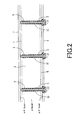
Fig. 1 is a plan view of a part of a solar cell according to the present invention as seen from a light-receiving surface side; and -
Fig. 2 is a sectional view taken along line II-II inFig. 1 . -
Figs. 1 and2 illustrate a typical example of a crystalline silicon solar cell comprising a first conductivity-type semiconductor layer 1, a second conductivity-type semiconductor layer 2, afirst electrode 3, and a second electrode 4. - The first conductivity-
type semiconductor layer 1 has a front side intended to serve as a light-receiving surface, while the second conductivity-type semiconductor layer 2 is disposed on the back side of the first conductivity-type semiconductor layer 1, forming a p-n junction together with the first conductivity-type semiconductor layer 1. More specifically, the second conductivity-type semiconductor layer 2 is a p-type silicon substrate, and the first conductivity-type semiconductor layer 1 being an n+ layer is formed at a light-receiving surface of the second conductivity-type semiconductor layer 2. Thus, the second conductivity-type semiconductor layer 2 being the p-type silicon substrate and the first conductivity-type semiconductor layer 1 being the n+ layer form the p-n junction. The second conductivity-type semiconductor layer 2 is most preferably a silicon crystal, but may also be a polycrystalline silicon or amorphous silicon. - The method for forming the first conductivity-
type semiconductor layer 1 being the n+ layer on the second conductivity-type semiconductor layer 2 being the p-type silicon substrate is well known as disclosed in Japanese Unexamined Patent Application Publication No.2009-123761 - An antireflection film 7 (or a protective film) is formed on a first major surface intended to serve as the light-receiving surface of the first conductivity-
type semiconductor layer 1. On the other hand, ap+ layer 6 is formed on a second major surface opposite from the light-receiving surface of the second conductivity-type semiconductor layer 2. On the back side of the second conductivity-type semiconductor layer 2, there is formed the second electrode 4. - The above structure can also be found in conventional solar cells. The present invention is characterized by the
first electrode 3. Thefirst electrode 3 passes through the second conductivity-type semiconductor layer 2 toward the first conductivity-type semiconductor layer 1 with a tip extending into and ending within the first conductivity-type semiconductor layer 1. Thefirst electrode 3 is covered with aninsulating film 5 at a portion that requires electrical insulation, for example, at a portion passing through the second conductivity-type semiconductor layer 2 and at a rear-end portion close to the second electrode 4. The tip extending into the first conductivity-type semiconductor layer 1 is not covered with theinsulating film 5. In the figure, the tip surface of thefirst electrode 3 is located at the same level as the surface of the first conductivity-type semiconductor layer 1 but may be slightly lowered. Arear end 31 of thefirst electrode 3 can be used as a terminal. - In the illustrated embodiment, the
first electrode 3 is formed by filling a conductive material into aminute hole 30 passing through the second conductivity-type semiconductor layer 2 and reaching the first conductivity-type semiconductor layer 1. Preferably, theminute holes 30 are distributed at a given area density. On an XY-plane of thesubstrate 1, preferably, theminute holes 30 are arranged at a given pitch distance Px, Py in a matrix form. The number of rows and the number of columns are arbitrary. Theminute hole 30 may have a hole diameter on the order of µ m. The pitch distance may be of such an order, too. - The
minute hole 30 can easily be formed by using a well-known drilling technique such as laser drilling process or chemical drilling process. Thefirst electrode 3 can be formed by filling a conductive paste or a molten metal into theminute hole 30 thus drilled. This process enables formation of densefirst electrodes 3 without leaving any void in the minute holes 30. A more desirable result can be obtained by hardening them while keeping the pressure. - The above pressure-filling type fabrication process belongs to a stamping and makes the cost of equipment considerably less expensive and requires less processing time, as compared with a conventional dry-etching process using an ICP-RIE. Thus, it is possible to achieve a low-cost solar cell.
- The
first electrode 3 may be formed by using a conductive paste, as described above, but is preferably formed by using a molten metal from the viewpoint of improving electrical characteristics and quality of the electrode itself. In this case, major examples of metal materials to be used include bismuth (Bi), indium (In), tin (Sn), and copper (Cu). Particularly, if bismuth (Bi) is contained, densefirst electrodes 3 can be formed without leaving any void or cavity in the minute holes 30 because of volume expansion characteristics of the bismuth (Bi) at the time of solidification. The molten metal may be prepared by melting powder of particles (nanoparticles) which are made of the above metal materials as aggregate of polycrystalline substances with a particle size of 1 µ m or less and a crystal size of 200 nm or less. - In the solar cell according to the present invention, as described above, since the p-n junction is formed between the second conductivity-
type semiconductor layer 2 and the first conductivity-type semiconductor layer 1, sunlight energy incident on the light-receiving surface can be transformed into a photoelectromotive force. - Here, since the
first electrode 3 passes through the second conductivity-type semiconductor layer 2 toward the first conductivity-type semiconductor layer 1 with a tip extending into and ending within the first conductivity-type semiconductor layer 1, thefirst electrode 3 does not appear on the light-receiving surface. Accordingly, thefirst electrode 3 does not block the incident light to cause a loss due to the shadow. This makes it possible to realize a solar cell having high light-receiving efficiency and power generation efficiency per unit area. - Moreover, since the
first electrode 3 has a current collecting effect on the first conductivity-type semiconductor layer 1, the conventionally indispensable light-receiving surface electrode becomes unnecessary, eliminating the limit in increasing the area. A large-area solar cell can be realized by arranging thefirst electrodes 3 at proper intervals, for example, in a matrix form. - Furthermore, since the
first electrode 3 passes through the second conductivity-type semiconductor layer 2 toward the first conductivity-type semiconductor layer 1, its connection to the outside can be located at the back side of the solar cell. The second electrode 4 is located at the back side of the solar cell from the first. Therefore, all electrodes such as bus bar electrodes and finger electrodes can be processed at the back side, preventing the incident light from being blocked by them to cause a loss due to the shadow. This makes it possible to realize a solar cell having high light-receiving efficiency and power generation efficiency per unit area. - The present invention is not limited to the crystalline silicon solar cell illustrated in the embodiment but is applicable to various types of solar cells, including a solar cell using a compound-semiconductor (e.g., CIGS), a solar cell using an organic semiconductor, and a multijunction solar cell having a plurality of p-n junctions, for example.
- Examples of silicon solar cells include a monocrystalline silicon type, a polycrystalline silicon type, a microcrystalline silicon type, an amorphous silicon type, and a thin-film silicon type, and also known are a hybrid type (HIT type) and so on.
- Examples of compound solar cells include an InGaAs solar cell, a GaAs-based solar cell, and a CIS-based (chalcopyrite-based) solar cell. The CIS-based (chalcopyrite-based) solar cell is the one using as a material of a light absorbing layer a I-III-VI group compound, called chalcopyrite, including Cu, In, Ga, Al, Se, S and so on, typified by Cu(In, Ga)Se2, Cu(In, Ga)(Se, S)2, and CuInS2, which are abbreviated as CIGS, CIGSS, and CIS, respectively.
- The present invention is applicable to any case, and in its application, the tip of the
first electrode 3 must be kept within the first conductivity-type semiconductor layer 1 so as to prevent the tip from projecting from the surface of the first conductivity-type semiconductor layer 1 that is closest to the light incidence surface. - While the present invention has been particularly shown and described with respect to preferred embodiments thereof, it will be understood by those skilled in the art that various changes in form and detail may be made therein without departing from the spirit, scope and teaching of the invention.
Claims (1)
- A solar cell comprising a first conductivity-type semiconductor layer (1), a second conductivity-type semiconductor layer (2), a first electrode (3), and a second electrode (4),
the first conductivity-type semiconductor layer (1) having a front side intended to serve as a light-receiving surface,
the second conductivity-type semiconductor layer (2) being disposed on a back side of the first conductivity-type semiconductor layer (1), forming a p-n junction together with the first conductivity-type semiconductor layer (1),
the first electrode (3) passing through the second conductivity-type semiconductor layer (2) toward the first conductivity-type semiconductor layer (1) with a tip extending into and ending within the first conductivity-type semiconductor layer (1),
the second electrode (4) being disposed at a back side of the solar cell.
Applications Claiming Priority (1)
| Application Number | Priority Date | Filing Date | Title |
|---|---|---|---|
| JP2010074919A JP2011210802A (en) | 2010-03-29 | 2010-03-29 | Solar cell |
Publications (1)
| Publication Number | Publication Date |
|---|---|
| EP2372778A2 true EP2372778A2 (en) | 2011-10-05 |
Family
ID=44280931
Family Applications (1)
| Application Number | Title | Priority Date | Filing Date |
|---|---|---|---|
| EP11250393A Withdrawn EP2372778A2 (en) | 2010-03-29 | 2011-03-28 | Solar cell |
Country Status (6)
| Country | Link |
|---|---|
| US (1) | US20110232740A1 (en) |
| EP (1) | EP2372778A2 (en) |
| JP (1) | JP2011210802A (en) |
| KR (1) | KR20110109900A (en) |
| CN (1) | CN102208457A (en) |
| TW (1) | TW201145540A (en) |
Families Citing this family (5)
| Publication number | Priority date | Publication date | Assignee | Title |
|---|---|---|---|---|
| JP5896378B2 (en) * | 2012-08-30 | 2016-03-30 | 日立造船株式会社 | CNT solar cell |
| JP2016058408A (en) * | 2013-01-31 | 2016-04-21 | パナソニック株式会社 | Photovoltaic device |
| CN105405909B (en) * | 2015-12-18 | 2017-01-25 | 英利能源(中国)有限公司 | MWT (Metallization Wrap Through) solar battery |
| CN111244231A (en) * | 2020-01-21 | 2020-06-05 | 浙江晶科能源有限公司 | Novel solar cell, preparation method thereof and photovoltaic system |
| CN112310233B (en) * | 2020-10-16 | 2022-06-14 | 泰州隆基乐叶光伏科技有限公司 | Solar cell, production method and cell module |
Citations (2)
| Publication number | Priority date | Publication date | Assignee | Title |
|---|---|---|---|---|
| JP2008270743A (en) | 2007-03-29 | 2008-11-06 | Kyocera Corp | Solar cell module |
| JP2009123761A (en) | 2007-11-12 | 2009-06-04 | Sharp Corp | Photoelectric conversion element and method for manufacturing the same |
Family Cites Families (11)
| Publication number | Priority date | Publication date | Assignee | Title |
|---|---|---|---|---|
| US5468652A (en) * | 1993-07-14 | 1995-11-21 | Sandia Corporation | Method of making a back contacted solar cell |
| AUPM483494A0 (en) * | 1994-03-31 | 1994-04-28 | Pacific Solar Pty Limited | Multiple layer thin film solar cells |
| US7170001B2 (en) * | 2003-06-26 | 2007-01-30 | Advent Solar, Inc. | Fabrication of back-contacted silicon solar cells using thermomigration to create conductive vias |
| US20060130891A1 (en) * | 2004-10-29 | 2006-06-22 | Carlson David E | Back-contact photovoltaic cells |
| US20070023082A1 (en) * | 2005-07-28 | 2007-02-01 | Venkatesan Manivannan | Compositionally-graded back contact photovoltaic devices and methods of fabricating such devices |
| KR101212198B1 (en) * | 2006-04-06 | 2012-12-13 | 삼성에스디아이 주식회사 | Solar cell |
| DE102006027737A1 (en) * | 2006-06-10 | 2007-12-20 | Hahn-Meitner-Institut Berlin Gmbh | Unilaterally contacted solar cell with plated-through holes and method of manufacture |
| CN101017858A (en) * | 2007-01-10 | 2007-08-15 | 北京市太阳能研究所有限公司 | A back contact solar battery and its making method |
| US20090283145A1 (en) * | 2008-05-13 | 2009-11-19 | Kim Yun-Gi | Semiconductor Solar Cells Having Front Surface Electrodes |
| GB0820684D0 (en) * | 2008-11-12 | 2008-12-17 | Silicon Cpv Plc | Photovoltaic solar cells |
| US8115097B2 (en) * | 2009-11-19 | 2012-02-14 | International Business Machines Corporation | Grid-line-free contact for a photovoltaic cell |
-
2010
- 2010-03-29 JP JP2010074919A patent/JP2011210802A/en active Pending
-
2011
- 2011-02-10 US US13/024,455 patent/US20110232740A1/en not_active Abandoned
- 2011-03-23 KR KR1020110025809A patent/KR20110109900A/en not_active Application Discontinuation
- 2011-03-28 EP EP11250393A patent/EP2372778A2/en not_active Withdrawn
- 2011-03-28 TW TW100110507A patent/TW201145540A/en unknown
- 2011-03-28 CN CN2011100755084A patent/CN102208457A/en active Pending
Patent Citations (2)
| Publication number | Priority date | Publication date | Assignee | Title |
|---|---|---|---|---|
| JP2008270743A (en) | 2007-03-29 | 2008-11-06 | Kyocera Corp | Solar cell module |
| JP2009123761A (en) | 2007-11-12 | 2009-06-04 | Sharp Corp | Photoelectric conversion element and method for manufacturing the same |
Also Published As
| Publication number | Publication date |
|---|---|
| TW201145540A (en) | 2011-12-16 |
| JP2011210802A (en) | 2011-10-20 |
| CN102208457A (en) | 2011-10-05 |
| KR20110109900A (en) | 2011-10-06 |
| US20110232740A1 (en) | 2011-09-29 |
Similar Documents
| Publication | Publication Date | Title |
|---|---|---|
| EP2253023B1 (en) | Solar module | |
| KR101440896B1 (en) | Thin film solar cell module and manufacturing method thereof | |
| US20140246070A1 (en) | Thin film solar module having series connection and method for the series connection of thin film solar cells | |
| US20130118569A1 (en) | Method for forming thin film solar cell with buffer-free fabrication process | |
| EP2485272A2 (en) | Solar power generation apparatus and manufacturing method thereof | |
| EP2372778A2 (en) | Solar cell | |
| US20220416107A1 (en) | Bifacial tandem photovoltaic cells and modules | |
| Benda | Photovoltaics towards terawatts–progress in photovoltaic cells and modules | |
| KR20150045309A (en) | Solar cell module | |
| Khoshsirat et al. | Copper-Indium-Gallium-Diselenide (CIGS) nanocrystalline bulk semiconductor as the absorber layer and its current technological trend and optimization | |
| US20110005585A1 (en) | Laser-Scribing Method to Make a Bifacial Thin Film Solar Cell and the Structure Thereof | |
| CN115249750B (en) | Photovoltaic cell, manufacturing method thereof and photovoltaic module | |
| WO2011014559A2 (en) | Lattice-matched chalcogenide multi-junction photovoltaic cell | |
| Söderström et al. | Low cost high energy yield solar module lines and its applications | |
| CN110459619B (en) | Selenium antimony sulfide battery pack and preparation method thereof | |
| Wirth | Photovoltaic Module Technology | |
| KR101241718B1 (en) | Solar cell module and method of fabricating the same | |
| US20120145232A1 (en) | Solar cell having improved rear contact | |
| EP2528106A1 (en) | Photovoltaic power generation device and manufacturing method thereof | |
| EP2876694A1 (en) | Solar cell | |
| CN112133787A (en) | Copper indium gallium selenide thin-film solar cell module and preparation method thereof | |
| Benda | Crystalline silicon cells and modules in present photovoltaics. | |
| EP3803985B1 (en) | Solar modul with an enlarged aperture area | |
| KR101273015B1 (en) | Solar cell apparatus and method of fabricating the same | |
| EP2251909A2 (en) | Solar cell structure and manufacturing method thereof |
Legal Events
| Date | Code | Title | Description |
|---|---|---|---|
| PUAI | Public reference made under article 153(3) epc to a published international application that has entered the european phase |
Free format text: ORIGINAL CODE: 0009012 |
|
| AK | Designated contracting states |
Kind code of ref document: A2 Designated state(s): AL AT BE BG CH CY CZ DE DK EE ES FI FR GB GR HR HU IE IS IT LI LT LU LV MC MK MT NL NO PL PT RO RS SE SI SK SM TR |
|
| AX | Request for extension of the european patent |
Extension state: BA ME |
|
| RAP1 | Party data changed (applicant data changed or rights of an application transferred) |
Owner name: NAPRA CO., LTD. |
|
| STAA | Information on the status of an ep patent application or granted ep patent |
Free format text: STATUS: THE APPLICATION IS DEEMED TO BE WITHDRAWN |
|
| 18D | Application deemed to be withdrawn |
Effective date: 20151001 |