EP2372508A2 - Improvements in or relating to optical navigation devices - Google Patents
Improvements in or relating to optical navigation devices Download PDFInfo
- Publication number
- EP2372508A2 EP2372508A2 EP11159021A EP11159021A EP2372508A2 EP 2372508 A2 EP2372508 A2 EP 2372508A2 EP 11159021 A EP11159021 A EP 11159021A EP 11159021 A EP11159021 A EP 11159021A EP 2372508 A2 EP2372508 A2 EP 2372508A2
- Authority
- EP
- European Patent Office
- Prior art keywords
- imaging
- imaging device
- illumination
- optical
- source
- Prior art date
- Legal status (The legal status is an assumption and is not a legal conclusion. Google has not performed a legal analysis and makes no representation as to the accuracy of the status listed.)
- Withdrawn
Links
Images


Classifications
-
- G—PHYSICS
- G06—COMPUTING OR CALCULATING; COUNTING
- G06F—ELECTRIC DIGITAL DATA PROCESSING
- G06F3/00—Input arrangements for transferring data to be processed into a form capable of being handled by the computer; Output arrangements for transferring data from processing unit to output unit, e.g. interface arrangements
- G06F3/01—Input arrangements or combined input and output arrangements for interaction between user and computer
- G06F3/03—Arrangements for converting the position or the displacement of a member into a coded form
- G06F3/041—Digitisers, e.g. for touch screens or touch pads, characterised by the transducing means
- G06F3/042—Digitisers, e.g. for touch screens or touch pads, characterised by the transducing means by opto-electronic means
-
- G—PHYSICS
- G06—COMPUTING OR CALCULATING; COUNTING
- G06F—ELECTRIC DIGITAL DATA PROCESSING
- G06F3/00—Input arrangements for transferring data to be processed into a form capable of being handled by the computer; Output arrangements for transferring data from processing unit to output unit, e.g. interface arrangements
- G06F3/01—Input arrangements or combined input and output arrangements for interaction between user and computer
- G06F3/03—Arrangements for converting the position or the displacement of a member into a coded form
- G06F3/0304—Detection arrangements using opto-electronic means
- G06F3/0317—Detection arrangements using opto-electronic means in co-operation with a patterned surface, e.g. absolute position or relative movement detection for an optical mouse or pen positioned with respect to a coded surface
-
- G—PHYSICS
- G06—COMPUTING OR CALCULATING; COUNTING
- G06F—ELECTRIC DIGITAL DATA PROCESSING
- G06F2203/00—Indexing scheme relating to G06F3/00 - G06F3/048
- G06F2203/041—Indexing scheme relating to G06F3/041 - G06F3/045
- G06F2203/04109—FTIR in optical digitiser, i.e. touch detection by frustrating the total internal reflection within an optical waveguide due to changes of optical properties or deformation at the touch location
Definitions
- the present invention relates to improvements in or relating to optical navigation devices such as, for example, optical mice.
- Computer devices are becoming ever smaller and full computing functionality can be found on phones and smart phones and other personal digital assistants (PDA). As the computer devices become smaller so the various features of the computer devices must also become smaller. This includes a requirement for smaller input systems for the user to enter inputs into the device.
- One such input system is an optical navigation device. Many computer devices, large and small, are equipped with optical navigation devices. However, with the smaller computer devices, minimizing the size of the optical navigation device can often be restrictive and problematic.
- Custom shaped illumination includes aesthetic and optical effects on the surface of the mouse which can have different uses.
- the present invention provides a method and system as set out in the accompanying claims.
- an imaging device of the type having an imaging surface and a sensor, wherein the imaging surface is illuminated by a first source and reflects at least some of the illumination to the sensor to detect an image, the imaging device having a predetermined width and an optical path passing therethrough, wherein the imaging device is also illuminated by a second source and wherein the illumination of the second source is directed to one or more predetermined regions on or near the imaging surface to produce an optical effect associated with the imaging surface.
- the present invention offers a number of benefits.
- the present invention provides a predetermined region on the surface of the element which can be used to show optical and aesthetic effects. These effects can be design related or of practical use.
- the effects are brought about by forming an optical element in a particular manner. The form ensures that the device remains thin and does not cost much to implement.
- the present invention relates to an imaging device associated with an optical navigation device.
- the optical navigation device is a mouse of small-scale which is intended to be operated by means of frustrated total internal reflection (F-TIR) in order to recognize the movement of a finger on an imaging surface.
- F-TIR frustrated total internal reflection
- This type of mouse is herein referred to as a fingermouse.
- Figure 1 a shows an example of a fingermouse 100 in accordance with the prior art.
- the fingermouse includes a base 102; an imaging element shown generally at 104; an LED 106 and a sensor 108.
- the top surface 110 of the imaging element 104 is a frustrated total internal reflection (F-TIR) surface.
- the imaging element includes a collimating lens 112 between the LED and the imaging element and an imaging lens 114 between the imaging element and the sensor.
- the imaging element further includes two total internal reflection mirror elements 116 which direct illumination from the collimating lens to the frustrated total internal reflection surface and then from the frustrated total internal reflection surface to the imaging lens.
- the lower surface 118 of the imaging element is substantially flat.
- Figure 1b shows the frustrated total internal reflection surface 110 with the LED 106 and the sensor 108 there below as viewed from above.
- the present invention provides custom shaped illumination, such as a ring, other shape or perimeter, to an optical device such as a fingermouse.
- custom shaped illumination such as a ring, other shape or perimeter
- an optical device such as a fingermouse.
- This is achieved by using a single light source, such as an LED and changing the shape of the imaging element. This enables the light source to be collimated onto an edge of the imaging element.
- the custom shaped illumination can be used to brighten the fingermouse and give rise to a number of aesthetic or optical effects. These effects can include showing logos; colors or moods on the mouse which are in tune with the phone or camera design, etc. Other uses include improved backlighting and illumination making the mouse easier to use in bad lighting conditions. Referring to figure 2 , the imaging element 200 of an optical device in accordance with an embodiment of the invention is shown.
- the imaging element 200 is illuminated by LED 202.
- the imaging element includes a curved surface 204, which is shaped in a predetermined manner, to ensure that illumination from the light source will be directed to certain areas of the top surface of the imaging element.
- the areas on the top surface are roughened areas 206 which scatter illumination from the source.
- the roughened surface is rough to the touch and can be any appropriate shape or size although in a preferred embodiment the roughened surface forms a circular ring or a square perimeter around the edge of the imaging element.
- a mask 208 is positioned to prevent illumination from the light source heading directly to the top surface of the imaging element.
- the mask can be replaced by an appropriate coating on the curved surface 204.
- the curved surface may be roughened so that additional backlighting is provided by the LED 202 at the top surface of the imaging element.
- the mask can incorporate a number of holes, forming a pattern, and coupled to a roughened curved surface to thereby produce a logo display on the top surface of the optical element when the mask is illuminated by the LED 202.
- Figure 3 shows a further embodiment of an optical element 300.
- the optical element 300 is illuminated by light source 302 and includes a mask 304.
- the various aspects of the light source and mask are equivalent to the earlier embodiment.
- the imaging element 300 includes a total internal reflection surface 306 which ensures that more light is directed to the roughened surface than in the figure 2 embodiment.
- the figure 3 embodiment includes one internal reflection surface 306 but it will be appreciated that a further surface can be provided on the opposite side.
- the optical element (200 or 300) can be made from any transparent material. However, due to the complexity of the various surfaces and shapes thereof a moldable material is preferred. Possible materials include polycarbonate, acrylics such as poly (methyl methacrylate) PMMA,
- Lexan 121 R Makrolon 2405, glass, Polyethylene, PVB (Polyvinyl butyral) or any other appropriate material.
- the optical imaging device includes an optical element 402, which may be shaped as previously described, or in any other appropriate shape.
- the device also includes a first light source 404, the illumination of which is focused onto a mousing surface 406 on the top surface of optical element 402.
- the mousing surface 406 responds to movement of a finger or other appropriate pointing device on the surface to set up the F-TIR of the illumination which are detected by the sensor 408.
- the F-TIR surface can reflect, absorb or scatter the illumination.
- the optical devices include a second light source 410 and a mask 412.
- the mask can be replaced by a coating on the curved surface 414 of the optical element 402 or by other appropriate means as earlier described.
- the illumination from the second light source is blocked from the mousing surface 406 by means of the mask. Any illumination that is not blocked by the mask is directed to roughened surfaces 416 around the edge of the optical element 402 by means of the shape and configuration of the optical element.
- the mousing surface 406 shows a reflection of the mask 418 and a ring 420 defining the roughened surface.
- the ring 420 comprises an upper ring 422 and a lower half ring 424.
- the ring is shown as straight sided with curved corners but could be any other shape including fully circular or any other straight edged form or perimeter depending on the optical element shape and any user requirements.
- the brightness of the ring 418 will depend upon the configuration of the optics of the fingermouse and could be dark or similar to the half rings depending on the shape, nature and orientation of the optical elements.
- FIG 5a a further embodiment of an optical device 500 is shown.
- the majority of the elements in the second embodiment are equivalent to those in the first embodiment of figure 4 and will not be described in further detail.
- the optical element 502 is formed in a different manner having a gap 504 between the upper surface of the optical element and the input and output end of the optical element for the purposes of illuminating the mousing surface 506. This gap provides a surface which refracts backlight to the roughened surface and changes the appearance of the mouse.
- the single LED in the centre may be changed for a combination of the several LEDs of different colors to allow for dynamic color change of the ring illumination.
- the orientation of the LED in the embodiment shown in figures 4 and 5 has the illumination being directed generally upwards.
- An alternative arrangement as shown in figure 6 provides a side emitting LED instead of the standard LED. This allows a greater degree of illumination to be collimated onto the ring surface and the LED can be closer to the optical element thereby reducing the size of the optical device.
- the optical element is formed accordingly to ensure the illumination travels in the required manner.
- the optical element may be of any form shape or size and adaptation may be made to accommodate different orientations of LED and other elements within the device.
- the sole requirement is that there are essentially two illumination sources: one from the first LED to illuminate a mousing surface and a second that enables illumination of a ring or other shape on the upper surface of the optical element.
- the examples presented here in have shown entire rings around the edge of the optical elements; however it would be appreciated that gaps may occur by positioning of certain masking elements to give different patterns.
- the illumination for mouse action is shown by a solid line and the illumination for custom shaped ring illumination is shown by a dotted line.
- the distance between the mousing surface and under the first LED or sensor in the present embodiment is in the region of 2.5 mm.
- This distance is the thickness of the imaging device and can vary between 2 mm and 3 mm. Ideally the thickness is not generally greater than 5 mm.
- the imaging device can be formed from a single piece molding.
- the molding includes each of the individual optical elements shown in the diagrams.
- the imaging device could alternatively be made in other appropriate ways with different optical elements which produce the same optical effect.
- the imaging device may also be made from a number of different elements, rather than a single molding.
- the technique for forming the imaging device may include techniques other than molding, such as replication, stamping, embossing or machining.
- the sensor is of any appropriate type and may be a CMOS sensor having an array of pixels for measuring reflected light at different locations to produce an image.
- the illumination sources are, for example, LEDs which may be of any appropriate type and may generate a source in the "optical" or non-optical ranges. Accordingly, reference to optics and optical are intended to cover wavelengths which are not in the human visible range.
- the optics which takes the illumination from the source to the imaging surface may be of any appropriate type.
- the imaging device is intended for use in an optical navigation device; however it will be appreciated that the imaging device could be used in any appropriate device, for example fingerprint reader or Lab-on-chip / Bio-Optical sensor systems (which detect chemi-fluorescence for medical and /or bio-testing applications).
- the optical navigation device may be used in any suitable devices such as a mobile or smart telephone, other personal or communications devices, a computer, a remote controller, access modules for doors and the like, a camera or any other suitable device.
Landscapes
- Engineering & Computer Science (AREA)
- General Engineering & Computer Science (AREA)
- Theoretical Computer Science (AREA)
- Human Computer Interaction (AREA)
- Physics & Mathematics (AREA)
- General Physics & Mathematics (AREA)
- Position Input By Displaying (AREA)
- Image Input (AREA)
- Geophysics And Detection Of Objects (AREA)
- Measurement Of Optical Distance (AREA)
- Length Measuring Devices By Optical Means (AREA)
Abstract
Description
- The present invention relates to improvements in or relating to optical navigation devices such as, for example, optical mice.
- Computer devices are becoming ever smaller and full computing functionality can be found on phones and smart phones and other personal digital assistants (PDA). As the computer devices become smaller so the various features of the computer devices must also become smaller. This includes a requirement for smaller input systems for the user to enter inputs into the device. One such input system is an optical navigation device. Many computer devices, large and small, are equipped with optical navigation devices. However, with the smaller computer devices, minimizing the size of the optical navigation device can often be restrictive and problematic.
- A number of devices have been proposed which offer thin thickness optical navigation devices. These have had some success but the designs have generally not solved all problems associated with thin imaging devices.
- One problem which remains unresolved is providing custom shaped illumination on optical devices, such as a fingermouse without having to resort to expensive or bulky options. Custom shaped illumination includes aesthetic and optical effects on the surface of the mouse which can have different uses.
- Previously lightpipes have been proposed as a means of custom shaping illumination. However, such lightpipes require a lot of space, typically several mm which would not be suitable for thin optical devices.
- It is an object of the present invention to overcome at least some of the problems associated with the prior art.
- It is a further object of the present invention to provide an optical navigation device having custom shaped illumination which does not add bulk or costs to the manufacture of the optical navigation device.
- The present invention provides a method and system as set out in the accompanying claims.
- According to one aspect of the present invention there is provided an imaging device of the type having an imaging surface and a sensor, wherein the imaging surface is illuminated by a first source and reflects at least some of the illumination to the sensor to detect an image, the imaging device having a predetermined width and an optical path passing therethrough, wherein the imaging device is also illuminated by a second source and wherein the illumination of the second source is directed to one or more predetermined regions on or near the imaging surface to produce an optical effect associated with the imaging surface.
- The present invention offers a number of benefits. The present invention provides a predetermined region on the surface of the element which can be used to show optical and aesthetic effects. These effects can be design related or of practical use. The effects are brought about by forming an optical element in a particular manner. The form ensures that the device remains thin and does not cost much to implement.
- Reference will now be made, by way of example, to the accompanying drawings, in which:
-
Figure 1 a is a cross-sectional diagram of an imaging device for an optical navigation device, in accordance with the prior art; -
Figure 1b is a view of the top surface of thefigure 1 a device; -
Figure 2 is a cross-sectional view of one imaging element for an optical navigation device, in accordance with an embodiment of the present invention; -
Figure 3 is a cross-sectional view of an alternative imaging element for an optical navigation device, in accordance with an embodiment of the present invention; -
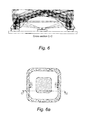
Figure 4a is a cross-sectional diagram of an imaging device for an optical navigation device, in accordance with an embodiment of the present invention; - Figure 4b is a top view of the
figure 4a device; -
Figure 5a is a cross-sectional diagram of an imaging device for an optical navigation device, in accordance with an embodiment of the present invention; - Figure 5b is a top view of the
figure 5a device; -
Figure 6a is a cross-sectional diagram of an imaging device for an optical navigation device, in accordance with an embodiment of the present invention; - Figure 6b is a top view of the
figure 6a device. - The present invention relates to an imaging device associated with an optical navigation device. The optical navigation device is a mouse of small-scale which is intended to be operated by means of frustrated total internal reflection (F-TIR) in order to recognize the movement of a finger on an imaging surface. This type of mouse is herein referred to as a fingermouse.
-
Figure 1 a shows an example of afingermouse 100 in accordance with the prior art. The fingermouse includes abase 102; an imaging element shown generally at 104; anLED 106 and asensor 108. Thetop surface 110 of theimaging element 104 is a frustrated total internal reflection (F-TIR) surface. In addition, the imaging element includes acollimating lens 112 between the LED and the imaging element and animaging lens 114 between the imaging element and the sensor. The imaging element further includes two total internalreflection mirror elements 116 which direct illumination from the collimating lens to the frustrated total internal reflection surface and then from the frustrated total internal reflection surface to the imaging lens. Thelower surface 118 of the imaging element is substantially flat. -
Figure 1b shows the frustrated totalinternal reflection surface 110 with theLED 106 and thesensor 108 there below as viewed from above. - The present invention provides custom shaped illumination, such as a ring, other shape or perimeter, to an optical device such as a fingermouse. This is achieved by using a single light source, such as an LED and changing the shape of the imaging element. This enables the light source to be collimated onto an edge of the imaging element. The custom shaped illumination can be used to brighten the fingermouse and give rise to a number of aesthetic or optical effects. These effects can include showing logos; colors or moods on the mouse which are in tune with the phone or camera design, etc. Other uses include improved backlighting and illumination making the mouse easier to use in bad lighting conditions. Referring to
figure 2 , theimaging element 200 of an optical device in accordance with an embodiment of the invention is shown. Theimaging element 200 is illuminated byLED 202. The imaging element includes acurved surface 204, which is shaped in a predetermined manner, to ensure that illumination from the light source will be directed to certain areas of the top surface of the imaging element. The areas on the top surface are roughenedareas 206 which scatter illumination from the source. The roughened surface is rough to the touch and can be any appropriate shape or size although in a preferred embodiment the roughened surface forms a circular ring or a square perimeter around the edge of the imaging element. - A
mask 208 is positioned to prevent illumination from the light source heading directly to the top surface of the imaging element. The mask can be replaced by an appropriate coating on thecurved surface 204. In an alternative arrangement, the curved surface may be roughened so that additional backlighting is provided by theLED 202 at the top surface of the imaging element. In a still further embodiment the mask can incorporate a number of holes, forming a pattern, and coupled to a roughened curved surface to thereby produce a logo display on the top surface of the optical element when the mask is illuminated by theLED 202. -
Figure 3 shows a further embodiment of anoptical element 300. Theoptical element 300 is illuminated bylight source 302 and includes amask 304. The various aspects of the light source and mask are equivalent to the earlier embodiment. Theimaging element 300 includes a totalinternal reflection surface 306 which ensures that more light is directed to the roughened surface than in thefigure 2 embodiment. Thefigure 3 embodiment includes oneinternal reflection surface 306 but it will be appreciated that a further surface can be provided on the opposite side. The optical element (200 or 300) can be made from any transparent material. However, due to the complexity of the various surfaces and shapes thereof a moldable material is preferred. Possible materials include polycarbonate, acrylics such as poly (methyl methacrylate) PMMA, - Lexan 121 R, Makrolon 2405, glass, Polyethylene, PVB (Polyvinyl butyral) or any other appropriate material.
- Referring to
figure 4a an optical imaging device is shown generally at 400. The optical imaging device includes anoptical element 402, which may be shaped as previously described, or in any other appropriate shape. The device also includes a firstlight source 404, the illumination of which is focused onto a mousingsurface 406 on the top surface ofoptical element 402. The mousingsurface 406 responds to movement of a finger or other appropriate pointing device on the surface to set up the F-TIR of the illumination which are detected by thesensor 408. The F-TIR surface can reflect, absorb or scatter the illumination. The optical devices include a secondlight source 410 and amask 412. The mask can be replaced by a coating on thecurved surface 414 of theoptical element 402 or by other appropriate means as earlier described. The illumination from the second light source is blocked from the mousingsurface 406 by means of the mask. Any illumination that is not blocked by the mask is directed to roughenedsurfaces 416 around the edge of theoptical element 402 by means of the shape and configuration of the optical element. - As can be seen in figure 4b the mousing
surface 406 shows a reflection of themask 418 and aring 420 defining the roughened surface. Thering 420 comprises anupper ring 422 and alower half ring 424. The ring is shown as straight sided with curved corners but could be any other shape including fully circular or any other straight edged form or perimeter depending on the optical element shape and any user requirements. The brightness of thering 418 will depend upon the configuration of the optics of the fingermouse and could be dark or similar to the half rings depending on the shape, nature and orientation of the optical elements. - Referring to
figure 5a a further embodiment of anoptical device 500 is shown. The majority of the elements in the second embodiment are equivalent to those in the first embodiment offigure 4 and will not be described in further detail. In the present embodiment theoptical element 502 is formed in a different manner having agap 504 between the upper surface of the optical element and the input and output end of the optical element for the purposes of illuminating themousing surface 506. This gap provides a surface which refracts backlight to the roughened surface and changes the appearance of the mouse. - It is possible to include more than one second source of illumination, for example two or more different colored LEDs. These can be separated from one another by an appropriate barrier. The result is a multicolored surface having different regions of the roughened surface being of different colors.
- In an alternative embodiment the single LED in the centre may be changed for a combination of the several LEDs of different colors to allow for dynamic color change of the ring illumination. The orientation of the LED in the embodiment shown in
figures 4 and5 has the illumination being directed generally upwards. An alternative arrangement as shown infigure 6 provides a side emitting LED instead of the standard LED. This allows a greater degree of illumination to be collimated onto the ring surface and the LED can be closer to the optical element thereby reducing the size of the optical device. In the side emitting light LED embodiment the optical element is formed accordingly to ensure the illumination travels in the required manner. - The optical element may be of any form shape or size and adaptation may be made to accommodate different orientations of LED and other elements within the device. The sole requirement is that there are essentially two illumination sources: one from the first LED to illuminate a mousing surface and a second that enables illumination of a ring or other shape on the upper surface of the optical element. The examples presented here in have shown entire rings around the edge of the optical elements; however it would be appreciated that gaps may occur by positioning of certain masking elements to give different patterns.
- In the diagrams the illumination for mouse action is shown by a solid line and the illumination for custom shaped ring illumination is shown by a dotted line.
- The distance between the mousing surface and under the first LED or sensor in the present embodiment is in the region of 2.5 mm. This distance is the thickness of the imaging device and can vary between 2 mm and 3 mm. Ideally the thickness is not generally greater than 5 mm. The imaging device can be formed from a single piece molding. The molding includes each of the individual optical elements shown in the diagrams. The imaging device could alternatively be made in other appropriate ways with different optical elements which produce the same optical effect. The imaging device may also be made from a number of different elements, rather than a single molding. The technique for forming the imaging device may include techniques other than molding, such as replication, stamping, embossing or machining.
- The sensor is of any appropriate type and may be a CMOS sensor having an array of pixels for measuring reflected light at different locations to produce an image.
- The illumination sources are, for example, LEDs which may be of any appropriate type and may generate a source in the "optical" or non-optical ranges. Accordingly, reference to optics and optical are intended to cover wavelengths which are not in the human visible range. The optics which takes the illumination from the source to the imaging surface may be of any appropriate type.
- The imaging device is intended for use in an optical navigation device; however it will be appreciated that the imaging device could be used in any appropriate device, for example fingerprint reader or Lab-on-chip / Bio-Optical sensor systems (which detect chemi-fluorescence for medical and /or bio-testing applications).
- The optical navigation device may be used in any suitable devices such as a mobile or smart telephone, other personal or communications devices, a computer, a remote controller, access modules for doors and the like, a camera or any other suitable device.
- There are many variations of the present invention which will be appreciated by the person skilled in the art and which are included within the scope of the present invention.
Claims (20)
- An imaging device of the type having an imaging surface and a sensor, wherein the imaging surface is illuminated by a first source and reflects at least some of the illumination to the sensor to detect an image, the imaging device having a predetermined width and an optical path passing therethrough, wherein the imaging device is also illuminated by a second source and wherein the illumination of the second source is directed to one or more predetermined regions on or near the imaging surface to produce an optical effect associated with the imaging surface.
- The imaging device of claim 1, wherein the illumination from the first source is reflected, absorbed or scattered by movement of a pointer moving relative to the imaging surface.
- The imaging device of claim 1 or claim 2, wherein the illumination from the second source is collimated by the shape of the imaging device to the one or more predetermined regions.
- The imaging device of claim 3, wherein the imaging device includes a lower curved surface for assisting with the collimation.
- The imaging device of any preceding claim, wherein the illumination from the second source does not directly reach the imaging surface.
- The imaging device of claim 5, wherein the imaging device includes a mask or a coating for preventing the second source directly illuminating the imaging surface.
- The imaging device of any preceding claim, wherein predetermined regions form an illuminated perimeter around the imaging surface.
- The imaging device of claim 7, wherein the perimeter is roughened to the touch.
- The imaging device of any preceding claim, formed from a single formed element.
- The imaging device of claim 9, wherein the single element is molded.
- A device including an imaging device, according to any preceding claim.
- The device of claim 11, in the form of an optical navigation device.
- The device of claim 12, wherein the optical navigation device is a mouse.
- The device of claim 13, wherein the mouse is a fingermouse.
- An apparatus including the device of any one of claims 11 to 14.
- The apparatus of claim 15, wherein the apparatus is a computer.
- The apparatus of claim 15, wherein the apparatus is a phone.
- The apparatus of claim 15, wherein the apparatus is a camera.
- The apparatus of claim 15, wherein the apparatus is a smart phone.
- The apparatus of claim 15, wherein the apparatus is a remote controller.
Applications Claiming Priority (1)
| Application Number | Priority Date | Filing Date | Title |
|---|---|---|---|
| GB201004810A GB201004810D0 (en) | 2010-03-23 | 2010-03-23 | Improvements in or relating to optical navigation devices |
Publications (2)
| Publication Number | Publication Date |
|---|---|
| EP2372508A2 true EP2372508A2 (en) | 2011-10-05 |
| EP2372508A3 EP2372508A3 (en) | 2013-01-09 |
Family
ID=42228159
Family Applications (1)
| Application Number | Title | Priority Date | Filing Date |
|---|---|---|---|
| EP11159021A Withdrawn EP2372508A3 (en) | 2010-03-23 | 2011-03-21 | Improvements in or relating to optical navigation devices |
Country Status (4)
| Country | Link |
|---|---|
| US (1) | US8988391B2 (en) |
| EP (1) | EP2372508A3 (en) |
| CN (1) | CN102253734B (en) |
| GB (1) | GB201004810D0 (en) |
Families Citing this family (8)
| Publication number | Priority date | Publication date | Assignee | Title |
|---|---|---|---|---|
| GB2494629A (en) * | 2011-09-09 | 2013-03-20 | St Microelectronics Res & Dev | Optical navigation device with sleep mode and active mode |
| US8553235B1 (en) * | 2012-01-18 | 2013-10-08 | Wen-Chieh Geoffrey Lee | High resolution and high sensitivity optically activated touch sensing device using multiple color light sources |
| US10210412B2 (en) | 2014-03-13 | 2019-02-19 | Pixart Imaging Inc. | Optical encoder capable of identifying absolute positions and operating method thereof |
| US10380445B2 (en) | 2014-03-13 | 2019-08-13 | Pixart Imaging Inc. | Optical encoder capable of identifying absolute positions and operating method thereof |
| TWI584158B (en) * | 2015-04-17 | 2017-05-21 | 原相科技股份有限公司 | Optical navigation chip, optical navigation module and optical encoder |
| EP3767448A3 (en) | 2015-01-07 | 2021-04-07 | Samsung Electronics Co., Ltd. | Display device and operating method thereof |
| WO2016111555A2 (en) * | 2015-01-07 | 2016-07-14 | Samsung Electronics Co., Ltd. | Bendable user terminal device and method for displaying thereof |
| US10976560B2 (en) | 2018-07-26 | 2021-04-13 | Pixart Imaging Inc. | Navigation device, illumination system and light beam shaping optics thereof |
Family Cites Families (25)
| Publication number | Priority date | Publication date | Assignee | Title |
|---|---|---|---|---|
| IL67722A0 (en) * | 1982-02-05 | 1983-05-15 | Plessey Overseas | Container with memory |
| US6061177A (en) * | 1996-12-19 | 2000-05-09 | Fujimoto; Kenneth Noboru | Integrated computer display and graphical input apparatus and method |
| EP0860755B1 (en) * | 1997-02-20 | 2002-06-12 | Asulab S.A. | Device for uniformly illuminating the dial of a display apparatus |
| US20010038381A1 (en) * | 1997-11-17 | 2001-11-08 | Richard W. Griencewic | Illuminated pointing device for a computer |
| US6590176B2 (en) * | 2001-03-12 | 2003-07-08 | Joseph W. Cole | Push-button type electrical switch |
| JP4100155B2 (en) * | 2002-12-05 | 2008-06-11 | オムロン株式会社 | Luminescent light source, luminescent light source array, and apparatus using the luminescent light source |
| EP1437677A1 (en) * | 2002-12-30 | 2004-07-14 | Nokia Corporation | Optical user interface for controlling portable electric device |
| US20070152977A1 (en) * | 2005-12-30 | 2007-07-05 | Apple Computer, Inc. | Illuminated touchpad |
| CN1619050A (en) * | 2003-11-17 | 2005-05-25 | 蒋亮健 | Electric iron temperature controlling identifying character display device |
| TWM259236U (en) | 2004-05-31 | 2005-03-11 | Wistron Corp | Electronic device |
| US7705835B2 (en) * | 2005-03-28 | 2010-04-27 | Adam Eikman | Photonic touch screen apparatus and method of use |
| US20060256086A1 (en) * | 2005-05-12 | 2006-11-16 | Tong Xie | Integrated optical mouse |
| JP2007226439A (en) | 2006-02-22 | 2007-09-06 | Sharp Corp | Display device and electronic device |
| US8441467B2 (en) * | 2006-08-03 | 2013-05-14 | Perceptive Pixel Inc. | Multi-touch sensing display through frustrated total internal reflection |
| WO2009020940A2 (en) * | 2007-08-03 | 2009-02-12 | Perceptive Pixel, Inc. | Multi-touch sensing through frustrated total internal reflection |
| KR101407300B1 (en) * | 2007-11-19 | 2014-06-13 | 엘지디스플레이 주식회사 | Multi touch flat display module |
| US8106885B2 (en) * | 2007-12-19 | 2012-01-31 | Research In Motion Limited | Input mechanism for handheld electronic communication device |
| US9213450B2 (en) * | 2008-11-17 | 2015-12-15 | Tpk Touch Solutions Inc. | Touch sensor |
| CN201348769Y (en) * | 2009-01-15 | 2009-11-18 | 苏州达方电子有限公司 | Transparent mouse |
| GB2470553A (en) * | 2009-05-26 | 2010-12-01 | St Microelectronics Ltd | Optical computer input with single frustrated total internal reflection mousing surface |
| TWM381126U (en) * | 2009-11-20 | 2010-05-21 | Micro Star Int Co Ltd | Electronic device with optical touch-controlled module |
| US8390569B2 (en) * | 2009-11-25 | 2013-03-05 | Research In Motion Limited | Optical trackpad module and method of using same |
| US8937598B2 (en) * | 2010-02-25 | 2015-01-20 | Blackberry Limited | Illuminated optical navigation module |
| US20110205179A1 (en) * | 2010-02-25 | 2011-08-25 | Research In Motion Limited | Three-dimensional illuminated area for optical navigation |
| GB2480621A (en) * | 2010-05-25 | 2011-11-30 | St Microelectronics | Calibration of optical navigation devices in ambient light conditions |
-
2010
- 2010-03-23 GB GB201004810A patent/GB201004810D0/en not_active Ceased
-
2011
- 2011-03-21 EP EP11159021A patent/EP2372508A3/en not_active Withdrawn
- 2011-03-22 US US13/053,520 patent/US8988391B2/en not_active Expired - Fee Related
- 2011-03-23 CN CN201110113333.1A patent/CN102253734B/en not_active Expired - Fee Related
Non-Patent Citations (1)
| Title |
|---|
| None |
Also Published As
| Publication number | Publication date |
|---|---|
| US8988391B2 (en) | 2015-03-24 |
| US20110234541A1 (en) | 2011-09-29 |
| CN102253734B (en) | 2017-05-10 |
| EP2372508A3 (en) | 2013-01-09 |
| CN102253734A (en) | 2011-11-23 |
| GB201004810D0 (en) | 2010-05-05 |
Similar Documents
| Publication | Publication Date | Title |
|---|---|---|
| US8988391B2 (en) | Optical navigation devices | |
| US9971084B2 (en) | Illumination structure for uniform illumination of keys | |
| TWI604492B (en) | Back light module and luminous keyboard applied to a luminous keyboard | |
| EP3260956B1 (en) | Non-contact input device and method | |
| KR102436320B1 (en) | Proximity and illuminance sensor, portable terminal including the same | |
| TWI730658B (en) | Backlight module applied to display panel | |
| CN102081483B (en) | Optical sensing module | |
| WO2012172302A1 (en) | Optical navigation device | |
| US10984969B1 (en) | Uniform illumination of keys on a flexible substrate | |
| TWI448973B (en) | A light guide module that improves image contrast | |
| WO2016183490A1 (en) | Uniform illumination of keys | |
| CN107688804B (en) | Image capturing device | |
| TWI585655B (en) | Optical plate structure for a touch panel, and touch display panel and touch liquid crystal display panel including the same | |
| EP2423793A2 (en) | Optical navigation device | |
| WO2018145322A1 (en) | Sensing device and terminal device | |
| CN209343363U (en) | Fingerprint Recognition Module | |
| EP2343634A2 (en) | Improvements in or relating to optical navigation devices | |
| US8537263B2 (en) | Optical navigation devices and associated methods | |
| TWI529563B (en) | Motion trajectory capturing device and motion trajectory capturing module thereof | |
| CN208672986U (en) | Backlight modules, liquid crystal display modules and electronic devices | |
| JP5196661B2 (en) | Light guide and pushbutton switch member using the same | |
| US11209294B2 (en) | Thin proximity sensing device | |
| US20130114296A1 (en) | Light guide apparatus and electronic device using the same | |
| TWI395245B (en) | Variable illuminating push-button device | |
| TWI585643B (en) | Electronic device |
Legal Events
| Date | Code | Title | Description |
|---|---|---|---|
| PUAI | Public reference made under article 153(3) epc to a published international application that has entered the european phase |
Free format text: ORIGINAL CODE: 0009012 |
|
| AK | Designated contracting states |
Kind code of ref document: A2 Designated state(s): AL AT BE BG CH CY CZ DE DK EE ES FI FR GB GR HR HU IE IS IT LI LT LU LV MC MK MT NL NO PL PT RO RS SE SI SK SM TR |
|
| AX | Request for extension of the european patent |
Extension state: BA ME |
|
| PUAL | Search report despatched |
Free format text: ORIGINAL CODE: 0009013 |
|
| AK | Designated contracting states |
Kind code of ref document: A3 Designated state(s): AL AT BE BG CH CY CZ DE DK EE ES FI FR GB GR HR HU IE IS IT LI LT LU LV MC MK MT NL NO PL PT RO RS SE SI SK SM TR |
|
| AX | Request for extension of the european patent |
Extension state: BA ME |
|
| RIC1 | Information provided on ipc code assigned before grant |
Ipc: G06F 3/033 20130101ALI20121130BHEP Ipc: G06F 3/042 20060101AFI20121130BHEP Ipc: G06F 3/03 20060101ALI20121130BHEP |
|
| 17P | Request for examination filed |
Effective date: 20130709 |
|
| RBV | Designated contracting states (corrected) |
Designated state(s): AL AT BE BG CH CY CZ DE DK EE ES FI FR GB GR HR HU IE IS IT LI LT LU LV MC MK MT NL NO PL PT RO RS SE SI SK SM TR |
|
| 17Q | First examination report despatched |
Effective date: 20131030 |
|
| STAA | Information on the status of an ep patent application or granted ep patent |
Free format text: STATUS: THE APPLICATION IS DEEMED TO BE WITHDRAWN |
|
| 18D | Application deemed to be withdrawn |
Effective date: 20151001 |