EP2372382A1 - Magnetic sensor, magnetic detector, and magnetic head - Google Patents
Magnetic sensor, magnetic detector, and magnetic head Download PDFInfo
- Publication number
- EP2372382A1 EP2372382A1 EP11153309A EP11153309A EP2372382A1 EP 2372382 A1 EP2372382 A1 EP 2372382A1 EP 11153309 A EP11153309 A EP 11153309A EP 11153309 A EP11153309 A EP 11153309A EP 2372382 A1 EP2372382 A1 EP 2372382A1
- Authority
- EP
- European Patent Office
- Prior art keywords
- magnetic
- channel
- hole
- layer
- magnetic sensor
- Prior art date
- Legal status (The legal status is an assumption and is not a legal conclusion. Google has not performed a legal analysis and makes no representation as to the accuracy of the status listed.)
- Granted
Links
- 230000005291 magnetic effect Effects 0.000 title claims abstract description 231
- 230000005294 ferromagnetic effect Effects 0.000 claims abstract description 95
- 230000005415 magnetization Effects 0.000 claims description 28
- 230000004888 barrier function Effects 0.000 claims description 24
- 230000005290 antiferromagnetic effect Effects 0.000 claims description 8
- 229910045601 alloy Inorganic materials 0.000 claims description 6
- 239000000956 alloy Substances 0.000 claims description 6
- 229910052742 iron Inorganic materials 0.000 claims description 6
- 229910052751 metal Inorganic materials 0.000 claims description 6
- 239000002184 metal Substances 0.000 claims description 6
- 229910052759 nickel Inorganic materials 0.000 claims description 5
- 239000004065 semiconductor Substances 0.000 claims description 5
- 229910001218 Gallium arsenide Inorganic materials 0.000 claims description 4
- 229910052804 chromium Inorganic materials 0.000 claims description 3
- 150000001875 compounds Chemical class 0.000 claims description 3
- 229910052748 manganese Inorganic materials 0.000 claims description 3
- 239000010410 layer Substances 0.000 description 204
- 230000004907 flux Effects 0.000 description 19
- XLOMVQKBTHCTTD-UHFFFAOYSA-N Zinc monoxide Chemical compound [Zn]=O XLOMVQKBTHCTTD-UHFFFAOYSA-N 0.000 description 6
- 230000000694 effects Effects 0.000 description 5
- 238000001514 detection method Methods 0.000 description 4
- 238000009792 diffusion process Methods 0.000 description 4
- 150000002500 ions Chemical class 0.000 description 4
- 238000000034 method Methods 0.000 description 4
- 238000001451 molecular beam epitaxy Methods 0.000 description 4
- 239000000758 substrate Substances 0.000 description 4
- 230000002401 inhibitory effect Effects 0.000 description 3
- 239000000463 material Substances 0.000 description 3
- 230000004044 response Effects 0.000 description 3
- 239000011787 zinc oxide Substances 0.000 description 3
- 240000006829 Ficus sundaica Species 0.000 description 2
- 206010028980 Neoplasm Diseases 0.000 description 2
- 238000000137 annealing Methods 0.000 description 2
- 201000011510 cancer Diseases 0.000 description 2
- 238000010894 electron beam technology Methods 0.000 description 2
- 239000003302 ferromagnetic material Substances 0.000 description 2
- 238000009877 rendering Methods 0.000 description 2
- 230000035945 sensitivity Effects 0.000 description 2
- FRWYFWZENXDZMU-UHFFFAOYSA-N 2-iodoquinoline Chemical compound C1=CC=CC2=NC(I)=CC=C21 FRWYFWZENXDZMU-UHFFFAOYSA-N 0.000 description 1
- 230000005355 Hall effect Effects 0.000 description 1
- GWEVSGVZZGPLCZ-UHFFFAOYSA-N Titan oxide Chemical compound O=[Ti]=O GWEVSGVZZGPLCZ-UHFFFAOYSA-N 0.000 description 1
- 238000009825 accumulation Methods 0.000 description 1
- 238000005452 bending Methods 0.000 description 1
- LTPBRCUWZOMYOC-UHFFFAOYSA-N beryllium oxide Inorganic materials O=[Be] LTPBRCUWZOMYOC-UHFFFAOYSA-N 0.000 description 1
- 230000000903 blocking effect Effects 0.000 description 1
- 230000008859 change Effects 0.000 description 1
- 239000004020 conductor Substances 0.000 description 1
- 239000000470 constituent Substances 0.000 description 1
- 230000008878 coupling Effects 0.000 description 1
- 238000010168 coupling process Methods 0.000 description 1
- 238000005859 coupling reaction Methods 0.000 description 1
- 230000007423 decrease Effects 0.000 description 1
- 230000003247 decreasing effect Effects 0.000 description 1
- 230000005358 geomagnetic field Effects 0.000 description 1
- 239000011810 insulating material Substances 0.000 description 1
- 239000012212 insulator Substances 0.000 description 1
- 239000007788 liquid Substances 0.000 description 1
- CPLXHLVBOLITMK-UHFFFAOYSA-N magnesium oxide Inorganic materials [Mg]=O CPLXHLVBOLITMK-UHFFFAOYSA-N 0.000 description 1
- 239000000395 magnesium oxide Substances 0.000 description 1
- AXZKOIWUVFPNLO-UHFFFAOYSA-N magnesium;oxygen(2-) Chemical compound [O-2].[Mg+2] AXZKOIWUVFPNLO-UHFFFAOYSA-N 0.000 description 1
- 230000005381 magnetic domain Effects 0.000 description 1
- 239000000696 magnetic material Substances 0.000 description 1
- 238000004519 manufacturing process Methods 0.000 description 1
- TWNQGVIAIRXVLR-UHFFFAOYSA-N oxo(oxoalumanyloxy)alumane Chemical compound O=[Al]O[Al]=O TWNQGVIAIRXVLR-UHFFFAOYSA-N 0.000 description 1
- 238000000206 photolithography Methods 0.000 description 1
- 229910000702 sendust Inorganic materials 0.000 description 1
- 239000002356 single layer Substances 0.000 description 1
- 238000000992 sputter etching Methods 0.000 description 1
- 239000000126 substance Substances 0.000 description 1
- OGIDPMRJRNCKJF-UHFFFAOYSA-N titanium oxide Inorganic materials [Ti]=O OGIDPMRJRNCKJF-UHFFFAOYSA-N 0.000 description 1
- 238000005406 washing Methods 0.000 description 1
Images




Classifications
-
- G—PHYSICS
- G01—MEASURING; TESTING
- G01R—MEASURING ELECTRIC VARIABLES; MEASURING MAGNETIC VARIABLES
- G01R33/00—Arrangements or instruments for measuring magnetic variables
- G01R33/12—Measuring magnetic properties of articles or specimens of solids or fluids
- G01R33/1284—Spin resolved measurements; Influencing spins during measurements, e.g. in spintronics devices
-
- B—PERFORMING OPERATIONS; TRANSPORTING
- B82—NANOTECHNOLOGY
- B82Y—SPECIFIC USES OR APPLICATIONS OF NANOSTRUCTURES; MEASUREMENT OR ANALYSIS OF NANOSTRUCTURES; MANUFACTURE OR TREATMENT OF NANOSTRUCTURES
- B82Y25/00—Nanomagnetism, e.g. magnetoimpedance, anisotropic magnetoresistance, giant magnetoresistance or tunneling magnetoresistance
-
- G—PHYSICS
- G01—MEASURING; TESTING
- G01R—MEASURING ELECTRIC VARIABLES; MEASURING MAGNETIC VARIABLES
- G01R33/00—Arrangements or instruments for measuring magnetic variables
- G01R33/02—Measuring direction or magnitude of magnetic fields or magnetic flux
- G01R33/06—Measuring direction or magnitude of magnetic fields or magnetic flux using galvano-magnetic devices
- G01R33/09—Magnetoresistive devices
- G01R33/093—Magnetoresistive devices using multilayer structures, e.g. giant magnetoresistance sensors
-
- G—PHYSICS
- G11—INFORMATION STORAGE
- G11B—INFORMATION STORAGE BASED ON RELATIVE MOVEMENT BETWEEN RECORD CARRIER AND TRANSDUCER
- G11B5/00—Recording by magnetisation or demagnetisation of a record carrier; Reproducing by magnetic means; Record carriers therefor
- G11B5/127—Structure or manufacture of heads, e.g. inductive
- G11B5/33—Structure or manufacture of flux-sensitive heads, i.e. for reproduction only; Combination of such heads with means for recording or erasing only
- G11B5/39—Structure or manufacture of flux-sensitive heads, i.e. for reproduction only; Combination of such heads with means for recording or erasing only using magneto-resistive devices or effects
- G11B2005/3996—Structure or manufacture of flux-sensitive heads, i.e. for reproduction only; Combination of such heads with means for recording or erasing only using magneto-resistive devices or effects large or giant magnetoresistive effects [GMR], e.g. as generated in spin-valve [SV] devices
-
- G—PHYSICS
- G11—INFORMATION STORAGE
- G11B—INFORMATION STORAGE BASED ON RELATIVE MOVEMENT BETWEEN RECORD CARRIER AND TRANSDUCER
- G11B5/00—Recording by magnetisation or demagnetisation of a record carrier; Reproducing by magnetic means; Record carriers therefor
- G11B5/127—Structure or manufacture of heads, e.g. inductive
- G11B5/33—Structure or manufacture of flux-sensitive heads, i.e. for reproduction only; Combination of such heads with means for recording or erasing only
- G11B5/39—Structure or manufacture of flux-sensitive heads, i.e. for reproduction only; Combination of such heads with means for recording or erasing only using magneto-resistive devices or effects
- G11B5/3903—Structure or manufacture of flux-sensitive heads, i.e. for reproduction only; Combination of such heads with means for recording or erasing only using magneto-resistive devices or effects using magnetic thin film layers or their effects, the films being part of integrated structures
- G11B5/3906—Details related to the use of magnetic thin film layers or to their effects
- G11B5/3909—Arrangements using a magnetic tunnel junction
Definitions
- the present invention relates to a magnetic sensor, a magnetic detector, and a magnetic head.
- Magnetic field detection devices of this type have been in use for HDD heads for detecting magnetic fields from minute areas, sensors for detecting the geomagnetic field, and the like.
- the magnetic field detection devices used for the HDD heads have been made finer.
- techniques for finely dividing the devices have been approaching their limits.
- finely dividing the devices has increased the device resistance, thereby hindering lower power consumption and higher speed operation. That is, there has been a trade-off between making magnetic fluxes from minute areas detectable and inhibiting the device resistance from increasing.
- the magnetic sensor in accordance with the present invention comprises a channel, a ferromagnetic body and first and second reference electrodes on the channel, a magnetic shield covering a part of the channel opposing the ferromagnetic body, and an insulating film disposed between the channel and the magnetic shield, wherein the magnetic shield has a through-hole extending toward the part of the channel opposing the ferromagnetic body.
- the ferromagnetic body functions not only as an injecting electrode for injecting spins into the channel but also as a receiving electrode for receiving the spins from the channel.
- the channel functions as a part accumulating the spins injected from the ferromagnetic body.
- the magnetic shield covering the part of the channel opposing the ferromagnetic body is provided with a through-hole extending toward the part of the channel opposing the ferromagnetic body.
- a voltage output or resistance output in response to the external magnetic field can be read by electrically connecting one of a current supply and an output meter to the ferromagnetic body and first reference electrode and electrically connecting the other to the ferromagnetic body and second reference electrode, whereby a value corresponding to the degree of rotation of spins depending on whether the external magnetic field exists or not can be detected.
- magnetic fluxes can be detected from a minute area corresponding to the size of the above-mentioned through-hole.
- the magnetic fluxes can be detected without making the size of the ferromagnetic body smaller, whereby the device resistance can be inhibited from being increased by finely dividing the ferromagnetic body. Since the insulating film is disposed between the channel and the magnetic shield, the magnetic shield can be inhibited from absorbing the spins.
- the through-hole has a whole cross section opposing the channel as seen from the axial direction of the through-hole.
- external magnetic fields can be read more accurately from desirable areas.
- the through-hole may have a bottom part having a diameter smaller than that of a top part thereof. That is, the through-hole may have a tapered side face.
- magnetic fluxes caused by external magnetic fields cannot be absorbed by the magnetic shield when obliquely incident on the channel. Therefore, the angle of incidence of external magnetic fields can be changed according to the taper angle of the tapered side face.
- the channel has a bent form, and the through-hole is disposed so as to oppose an outer side face of a bend of the channel.
- an area for reading magnetic fluxes of external magnetic fields and the like can be made compact.
- the ferromagnetic body has a direction of magnetization pinned by an antiferromagnetic body disposed on the ferromagnetic body.
- the direction of magnetization of the ferromagnetic body can be provided with unidirectional anisotropy. This can yield the ferromagnetic body having a higher coercive force in one direction than when no antiferromagnetic body is provided.
- the magnetic sensor further comprises a permanent magnet for supplying the through-hole with a magnetic field oriented in the axial direction of the through-hole.
- a permanent magnet for supplying the through-hole with a magnetic field oriented in the axial direction of the through-hole.
- an output peak appears when the external magnetic field to be inspected is zero.
- the output peak position can be shifted, so that an output peak can be generated when the external magnetic field is not zero.
- the ferromagnetic body is made of a metal selected from the group consisting of Cr, Mn, Co, Fe, and Ni, an alloy containing at least one element selected from the group, or a compound containing at least one element selected from the group and at least one element selected from the group consisting of B, C, N, Si, and Ge.
- They are ferromagnetic materials with high spin polarizability and thus can favorably achieve a function as a spin-injecting or spin-receiving electrode.
- the channel is made of a semiconductor containing at least one of Si, Ge, GaAs, C, and ZnO.
- a semiconductor has a relatively large spin-diffusion length, whereby spins can favorably be accumulated within the channel.
- a barrier layer is formed between the ferromagnetic body and the channel. This makes it possible for a large number of spin-polarized electrons to be injected from the ferromagnetic body into the channel, whereby the potential output of the magnetic sensor can be enhanced.
- a magnetic detector comprises a plurality of such magnetic sensors.
- respective outputs of the magnetic sensors can be combined.
- Such a magnetic detector can be employed in a biosensor for detecting cancer cells and the like, for example.
- a magnetic head may comprise a reading head part having the above-mentioned magnetic sensor and a recording head part for writing. This can provide a new magnetic head utilizing the so-called Hanle effect.
- the present invention can provide a magnetic sensor which can detect magnetic fluxes from minute areas and inhibit the device resistance from increasing.
- Fig. 1 is a top plan view of a magnetic sensor
- Fig. 1 is a top plan view of the magnetic sensor in accordance with the first embodiment.
- Fig. 2 is a sectional view taken along the line II-II of Fig. 1 .
- a magnetic sensor 1 comprises a channel layer 7, a ferromagnetic layer 12, and a magnetic shield layer and detects external magnetic fields along the Z axis.
- the channel layer 7 functions as a part accumulating spins injected from the ferromagnetic layer 12.
- the channel layer 7 has a rectangular form as seen from the thickness direction of the channel layer 7.
- the channel layer 7 may be doped with ions for rendering it electrically conductive.
- the ion content may be 1.0 ⁇ 10 15 to 1.0 ⁇ 10 22 cm -3 , for example.
- the channel layer 7 is made of a material having a long spin life, an example of which is a semiconductor containing at least one of Si, Ge, GaAs, C, and ZnO.
- the ferromagnetic layer 12 functions not only as an injecting electrode for injecting spins into the channel layer 7 but also as a receiving electrode for detecting the spins within the channel layer.
- the ferromagnetic layer 12 is disposed on a first region 71 of the channel layer 7.
- the ferromagnetic layer 12 has a rectangular parallelepiped form whose longer axis is oriented in the Y axis.
- the direction of magnetization G 1 of the ferromagnetic layer 12 is nonparallel to the direction of magnetization B of an external magnetic field B.
- the ferromagnetic layer 12 is made of a ferromagnetic material.
- the magnetic shield layer covers a part of the channel layer 7 opposing the ferromagnetic layer 12.
- the magnetic shield layer covers the surface of the channel layer 7 at least partly while interposing an insulating film (e.g., insulating film 7a) therebetween, thereby blocking external magnetic fields from entering the channel layer 7.
- the magnetic shield layer covers a part about the first region 71 which opposes the ferromagnetic layer 12.
- the example illustrated in Fig. 2 uses a lower magnetic shield layer S1 as the magnetic shield layer.
- the lower magnetic shield layer S1 is disposed under the channel layer 7.
- the magnetic shield layer has a through-hole H extending toward the part of the channel layer 7 opposing the ferromagnetic layer 12.
- the through-hole H is used for applying an external magnetic field to the channel layer 7.
- the through-hole H is formed in the lower magnetic shield layer S1 and arranged so as to oppose the lower face of the first region 71 of the channel layer 7.
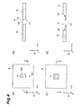
- Fig. 4(a) is a top plan view illustrating an example of the through-hole H formed in the magnetic shield layer S.
- the through-hole H can attain various forms, an example of which is a rectangle.
- the through-hole H has an oblong form as seen from the thickness direction of the magnetic shield layer S (the Z axis).
- letting the shorter-side length (X-axis length) D1 of the through-hole H be 0.003 to 0.3 ⁇ m, for example, its longer-side length (Y-axis length) D2 may be 0.01 to 1 ⁇ m, for example.
- Fig. 4(b) is a sectional view taken along the line B1-B1 of Fig. 4(a) .
- the bottom part h1 of the through-hole H may have a size identical to that of its top part h2.
- the through-hole H extends vertically toward the channel layer 7.
- Examples of the material for the magnetic shield layer include soft magnetic materials such as alloys containing Ni and Fe, sendust, alloys containing Fe and Co, and alloys containing Fe, Co, and Ni.
- the magnetic sensor 1 further comprises a first reference electrode 20A and a second reference electrode 20B.
- the first reference electrode 20A is disposed on a second region 72 of the channel layer 7.
- the second reference electrode 20B is disposed on a third region 73 of the channel layer 7.
- Each of the first and second reference electrodes 20A, 20B is made of an electrically conductive material, which is constituted by a nonmagnetic metal, such as A1, having a resistance lower than that of Si.
- the first region 71 exists between the second and third regions 72, 73 of the channel layer 7. That is, the first reference electrode 20A, ferromagnetic layer 12, and second reference electrode 20B are arranged in this order with predetermined gaps along the X axis on the channel layer 7.
- the distance between the first reference electrode 20A and the ferromagnetic layer 12 is longer than the spin-diffusion length by which electrons can keep their spins in the channel layer 7.
- the distance between the second reference electrode 20B and the ferromagnetic layer 12 is also longer than the spin-diffusion length in the channel layer 7. This structure can inhibit the first and second reference electrodes 20A, 20B from absorbing spins and lowering output.
- the channel layer 7 is made of Si
- the spin-diffusion length is about 2.5 ⁇ m, for example.
- the magnetic sensor 1 further comprises a barrier layer 81.
- the barrier layer 81 is disposed between the channel layer 7 and the ferromagnetic layer 12. This makes it possible for a large number of spin-polarized electrons to be injected from the ferromagnetic layer 12 into the channel layer 7, whereby the potential output of the magnetic sensor can be enhanced.
- the barrier layer 81 is a tunnel barrier made of a film of an insulating material.
- the barrier layer 81 is constituted by a single layer in the example illustrated in Fig. 2 but may have a multilayer structure constructed by a plurality of layers. For example, layers made of magnesium oxide, aluminum oxide, titanium oxide, zinc oxide, and beryllium oxide may be used as the barrier layer 81.
- the barrier layer 81 has a thickness of 3 nm or less.
- the barrier layer 81 has a thickness of 0.4 nm or more.
- the magnetic sensor 1 further comprises an insulating film (or insulator).
- the insulating film functions to prevent the channel layer 7 from being exposed and insulate the channel layer 7 electrically and magnetically.
- the insulating film exists between the magnetic shield layer and the channel layer 7. This is effective in inhibiting the spin flow flowing through the channel layer 7 from flowing out to the magnetic shield layer in particular.
- the insulating film covers a necessary region on a surface (e.g., a lower, side, or upper face) of the channel layer 7. In the example illustrated in Fig. 2 , insulating films 7a, 7b are disposed on the lower and upper faces of the channel layer 7, respectively.
- the insulating film 7b is arranged on the upper face of the region existing between the second and third regions 72, 73. Leads connecting with the first reference electrode 20A, ferromagnetic layer 12, and second reference electrode 20B can be restrained from absorbing spins of the channel layer 7 when arranged on the insulating film 7b. When the leads are placed on the insulating film 7b, currents can also be kept from flowing from the leads to the channel layer 7.
- the lower magnetic shield layer S1 is disposed on the lower face of the channel layer 7 with the insulating film 7a interposed therebetween.
- alignment marks are formed on a substrate prepared beforehand.
- a substrate an AlTiC substrate may be used, for example.
- the lower magnetic shield layer S1 is formed on the substrate.
- the insulating film 7a is formed on the lower magnetic shield layer S 1 by molecular beam epitaxy (MBE), for example.
- MBE molecular beam epitaxy
- the channel layer 7 is formed on the insulating film 7a by MBE, for example.
- Ions for rendering the channel layer 7 electrically conductive are injected therein, so as to adjust the conductive characteristic of the channel layer 7.
- the ions are diffused by thermal annealing when necessary.
- attached substances, organic matters, and oxide films are washed away from the surface of the channel layer 7.
- a diluted HF solution is used as a washing liquid.
- a barrier film to become the barrier layer 81 and a ferromagnetic film to become the ferromagnetic layer 12 are formed in this order on the channel layer 7 by MBE, for example.
- An antiferromagnetic layer may further be formed on the ferromagnetic layer 12 by MBE, for example, when necessary.
- annealing under a magnetic field is carried out in order to pin the direction of magnetization of the ferromagnetic layer 1.
- the barrier film and ferromagnetic film are processed through a mask by an electron beam (EB) method, for example. This forms the ferromagnetic layer 12 on the barrier layer 81 on the first second region 71 of the channel layer 7.
- unnecessary barrier and ferromagnetic films formed on the channel layer 7 are removed by ion milling, for example.
- the insulating film 7b is formed on the channel layer 7 free of the unnecessary barrier and ferromagnetic films. Also, the insulating film 7b is removed from the second and third regions 72, 73 of the channel layer 7, and the first and second reference electrodes 20A, 20B are formed there, respectively.
- the first and second reference electrodes 20A, 20B are formed by Al, for example.
- the lower magnetic shield layer S1 is formed so as to cover the part (i.e., the first region 71) of the channel layer 7 opposing the ferromagnetic layer 12 while interposing the insulating film 7a therebetween.
- the lower magnetic shield layer S1 is formed so as to cover regions adjacent to the first region 71 of the channel layer 7 as well.
- the lower magnetic shield layer S1 is provided with the through-hole H for magnetic fluxes from external magnetic fields to enter.
- the through-hole H can be formed by photolithography, for example. The foregoing method can produce the magnetic sensor 1 illustrated in Figs. 1 and 2 .
- Fig. 3 is a side view for explaining operations of the magnetic sensor 1 in accordance with the first embodiment.
- the direction of magnetization of the ferromagnetic layer 12 is pinned.
- the direction of magnetization G1 of the ferromagnetic layer 12 (along the X axis in the example illustrated in Fig. 3 ) is pinned nonparallel to the magnetic field direction of the external magnetic field B (the Z axis in the example illustrated in Fig. 3 ).
- connecting the ferromagnetic layer 12 and first reference electrode 20A to a current supply 70 can cause a detection current to flow through the ferromagnetic layer 12.
- a current flows from the ferromagnetic layer 12, which is a ferromagnetic body, to the nonmagnetic channel layer 7 through the barrier layer 81, electrons having a spin oriented in the direction corresponding to the direction of magnetization G1 of the ferromagnetic layer 12 are injected into the channel layer 7.
- the injected spins accumulate within the channel layer 7.
- the resistance output or voltage output attains a local extreme value when the external magnetic field B is zero.
- the local extreme value may be a local maximum or local minimum depending on the direction of the current or magnetization.
- the output can be evaluated by an output meter such as a voltmeter 80 connected to the ferromagnetic layer 12 and second reference electrode 20B.
- the direction of spins of the channel layer 7 rotates, thus failing to orient in the direction of magnetization G1 of the ferromagnetic layer 12.
- the resistance output or voltage output becomes less than a local maximum when the external magnetic field B is applied in the case where the local maximum would be attained if the external magnetic field B were zero, and more than a local minimum when the external magnetic field B is applied in the case where the local minimum would be attained if the external magnetic field B were zero.
- the output peak appears when the external magnetic field B is zero, and the output decreases as the external magnetic field B is increased or decreased. That is, the output varies depending on whether there is the external magnetic field B or not, whereby the magnetic sensor 1 in accordance with this embodiment can be used as a magnetic detection device.
- the through-hole H formed in the magnetic shield layer minute magnetic fluxes corresponding to the size of the through-hole H can be detected.
- the resolution is determined by the size of the through-hole H, whereby magnetic fluxes can be detected from small areas without finely dividing the size of the ferromagnetic layer 12. Therefore, the device resistance can also be inhibited from being increased by finely dividing the ferromagnetic layer 12.
- the magnetic sensor of the present invention yields the output peak when the external magnetic field is zero as mentioned above.
- the output peak appears at a zero point where magnetic fields of a magnetic domain wall cancel each other out, whereby it can be determined that inversion has occurred there.
- the magnetic sensor of the present invention is also characterized by its lack of hysteresis.
- Fig. 4(c) is a top plan view illustrating a mode of the through-hole in the magnetic shield layer S.
- Fig. 4(d) is a sectional view taken along the line D-D of Fig. 4(c) .
- the bottom part h1 of the through-hole H may have a diameter smaller than that of the top part h2 of the through-hole H. That is, the through-hole H may have a tapered side face.
- Fig. 5(a) is a top plan view illustrating a mode of the through-hole in the magnetic shield layer S.
- Fig. 5(b) is a sectional view taken along the line B2-B2 of Fig. 5(a).
- Fig. 5(c) is a sectional view taken along the line C-C of Fig. 5(a) .
- the through-hole H has a rectangular form as seen from the thickness direction of the magnetic shield layer S (the Z axis)
- its shorter sides may be provided with tapered side faces while keeping the longer sides free of tapered side faces. That is, as illustrated in Fig.
- the bottom part h1 may have the same diameter as with the top part h2 in the longer-side direction of the through-hole H.
- the bottom part h1 of the through-hole H may have a diameter smaller than that of the top part h2 of the through-hole H as illustrated in Fig. 5(c) . This can also change the angle of incidence of the external magnetic field B according to the taper angle ⁇ .
- the magnetic sensor further comprises a permanent magnet for supplying the through-hole H with a magnetic field oriented in the axial direction of the through-hole H.
- Fig. 6 is a top plan view illustrating an example in which the magnetic sensor is equipped with a permanent magnet.
- the magnetic sensor 1 illustrated in Fig. 6 further comprises a permanent magnet 8 on the insulating film 7b formed on the upper face of the channel layer 7.
- the permanent magnet 8 is adapted to generate a magnetic field Zl oriented in the axial direction of the through-hole H ( ⁇ Z directions in the example of Fig. 6 ) and applies a magnetic field oriented in the axial direction of the through-hole H ( ⁇ Z directions) to the first region 71 of the channel layer 7.
- the output peak can be issued when the external magnetic field B is not zero by applying a magnetic field to the channel layer 7 with the permanent magnet 8.
- the ferromagnetic layer 12 and the permanent magnet 8 are arranged with a gap therebetween in order to prevent them from magnetically coupling with each other.
- an insulating film may be provided between the ferromagnetic layer 12 and the permanent magnet 8.
- the through-hole H may be formed in a side magnetic shield layer covering a side face of the channel layer 7, for example.
- Fig. 7 is a side view illustrating Modified Example 1 of the magnetic sensor.
- the through-hole H is formed in a side magnetic shield layer S10.
- This magnetic sensor 2 detects external magnetic fields along the Y axis.
- the through-hole H is arranged such as to oppose a side face of the channel layer 7 existing in the region under the ferromagnetic layer 12. That is, when the through-hole H is formed in the side magnetic shield layer S, no through-hole is formed in the lower magnetic shield layer. As a consequence, external magnetic fields can be read from the side face of the channel layer 7.
- the direction of magnetization G4 of the ferromagnetic layer 12 (the Z axis in the example of Fig. 7 ) is nonparallel to the direction of magnetization of the applied external magnetic field (e.g., the Y axis) in this case as well.
- the channel layer 7 may have a form other than rectangles when seen from the thickness direction.
- Fig. 8 is a top plan view illustrating Modified Example 2 of the magnetic sensor.
- Fig. 9 is a side view illustrating a cross section taken along the line J-J of Fig. 8 .
- the channel layer 7 has a bent form as seen from the thickness direction of the channel layer 7 (the Z axis).
- the magnetic sensor 3 illustrated in Fig. 8 detects external magnetic fields along the Y axis.
- the channel layer 7 is disposed under the insulating film 7b and thus is not depicted in Fig. 8 .
- the through-hole H is arranged such as to oppose an outer side face KS of a bend K of the channel layer 7 having the bent form.
- the through-hole H is provided in a side magnetic shield layer S11 covering a side face of the channel layer 7.
- the outer side face KS of the bend K of the channel layer 7 is made flat, and the side magnetic shield layer S11 is formed along the outer side face KS.
- the surface for reading external magnetic fields is flat, so that magnetic fields can easily be detected when this flat surface KS opposes a surface to be read of a recording medium, for example.
- Figs. 8 and 9 illustrate an example in which the direction of magnetization G5 of the ferromagnetic layer 12 is pinned to the X axis. In this case, external magnetic fields can be applied from the Y axis, for example.
- the permanent magnet 8 may further be arranged such as to oppose the upper and lower faces of the bend K of the channel layer 7, thereby feeding the through-hole H with a magnetic field oriented in the Y axis.
- a magnetic detector may comprise a plurality of such magnetic sensors. In this case, respective outputs of the magnetic sensors can be combined.
- Such a magnetic detector can be employed in a biosensor for detecting cancer cells and the like, for example.
- a plurality of such magnetic sensors may be arranged in parallel or laminated, so as to form a magnetic detector.
- Fig. 10 is a side view illustrating Modified Example 3 of the magnetic sensor. As an example, Fig. 10 illustrates a structure in which a plurality of magnetic sensors 3 each depicted in Fig. 9 are laminated.
- the magnetic field for pinning the direction of magnetization of the ferromagnetic layer 12 is greater than the external magnetic field B to be evaluated. This allows the external magnetic field B to be detected stably.
- the above-mentioned magnetic sensor can be employed in a reading head part in a magnetic head equipped with a recording head part for writing, for example. This makes it possible to provide a magnetic head which can detect magnetic fluxes from minute areas of recording media and the like, for example.
- the current supply 70 and the output meter may exchange their places. That is, the ferromagnetic layer 12 and first reference electrode 20A may be connected to the output meter, while making the ferromagnetic layer 12 and second reference electrode 20B connect with the current supply 70. In this case, the ferromagnetic layer 12 functions as receiving and injecting electrodes.
- the barrier layer 81 is a tunnel barrier made of an insulating film.
- the barrier layer 81 may be a tunnel barrier made of a metal film. In this case, it may constitute a Schottky barrier between the semiconductor channel layer 7 and the metal barrier layer 81.
- the direction of magnetization of the ferromagnetic layer 12 may be pinned by an antiferromagnetic body disposed on the ferromagnetic layer 12.
- the above-mentioned magnetic sensor may further comprise an antiferromagnetic layer, disposed on the ferromagnetic layer 12, for pinning the direction of magnetization. This can yield the ferromagnetic layer 12 having a higher coercive force in one direction than when no antiferromagnetic layer is provided.
- the direction of spins injected into the channel layer 7 rotates about the axis of the applied magnetic field. If the axial direction of the through-hole is parallel to the direction of magnetization of the ferromagnetic layer, no rotation will occur in the direction of spins in response to the external magnetic field applied, thus making it hard to detect magnetic fluxes. Hence, such magnetic fluxes can be detected favorably when the axial direction of the through-hole H is nonparallel to the direction of magnetization of the ferromagnetic layer 12.
- the direction of magnetization of the ferromagnetic layer 12 may be parallel to its surface opposing the channel layer 7 as in Fig. 3 or 8 or perpendicular thereto as in Fig. 7 .
- each of the channel, ferromagnetic body, and magnetic shield may be made spherical or circular cylindrical, for example.
Landscapes
- Physics & Mathematics (AREA)
- Condensed Matter Physics & Semiconductors (AREA)
- General Physics & Mathematics (AREA)
- Chemical & Material Sciences (AREA)
- Engineering & Computer Science (AREA)
- Nanotechnology (AREA)
- Crystallography & Structural Chemistry (AREA)
- Hall/Mr Elements (AREA)
- Measuring Magnetic Variables (AREA)
- Magnetic Heads (AREA)
Abstract
Description
- The present invention relates to a magnetic sensor, a magnetic detector, and a magnetic head.
- Various devices for detecting external magnetic fields have conventionally been known, examples of which include Hall effect devices, MI (Magneto Impedance) devices, MR (Magneto Resistive) devices, GMR (Giant Magneto Resistive) devices, TMR (Tunnel Magneto Resistive) devices, and spin accumulation devices (see Japanese Patent Application Laid-Open No.
2007-299467 - For detecting magnetic fluxes from a smaller area, the magnetic field detection devices used for the HDD heads have been made finer. However, techniques for finely dividing the devices have been approaching their limits. On the other hand, finely dividing the devices has increased the device resistance, thereby hindering lower power consumption and higher speed operation. That is, there has been a trade-off between making magnetic fluxes from minute areas detectable and inhibiting the device resistance from increasing.
- For solving the problem mentioned above, it is an object of the present invention to provide a magnetic sensor which can detect magnetic fluxes from minute areas and inhibit the device resistance from increasing.
- For achieving the above-mentioned object, the magnetic sensor in accordance with the present invention comprises a channel, a ferromagnetic body and first and second reference electrodes on the channel, a magnetic shield covering a part of the channel opposing the ferromagnetic body, and an insulating film disposed between the channel and the magnetic shield, wherein the magnetic shield has a through-hole extending toward the part of the channel opposing the ferromagnetic body.
- The ferromagnetic body functions not only as an injecting electrode for injecting spins into the channel but also as a receiving electrode for receiving the spins from the channel. The channel functions as a part accumulating the spins injected from the ferromagnetic body. In this magnetic sensor, the magnetic shield covering the part of the channel opposing the ferromagnetic body is provided with a through-hole extending toward the part of the channel opposing the ferromagnetic body. When an external magnetic field is applied to the channel through the through-hole, the spins accumulated in the channel rotate their direction about the axis of the applied magnetic field (so-called Hanle effect). When no external magnetic field is applied to the channel, on the other hand, the spins accumulate within the channel as they are without changing their direction within the channel. Therefore, a voltage output or resistance output in response to the external magnetic field can be read by electrically connecting one of a current supply and an output meter to the ferromagnetic body and first reference electrode and electrically connecting the other to the ferromagnetic body and second reference electrode, whereby a value corresponding to the degree of rotation of spins depending on whether the external magnetic field exists or not can be detected. Hence, magnetic fluxes can be detected from a minute area corresponding to the size of the above-mentioned through-hole. Here, the magnetic fluxes can be detected without making the size of the ferromagnetic body smaller, whereby the device resistance can be inhibited from being increased by finely dividing the ferromagnetic body. Since the insulating film is disposed between the channel and the magnetic shield, the magnetic shield can be inhibited from absorbing the spins.
- Preferably, an axial direction of the through-hole is nonparallel to a direction of magnetization of the ferromagnetic body.
- When an external magnetic field is applied to the channel through the through-hole, spins within the channel rotate their direction about the axis of the applied magnetic field as mentioned above. If the axial direction of the through-hole and the direction of magnetization of the ferromagnetic body are parallel to each other, the spins will not rotate their direction in response to the external magnetic flux applied thereto, thus making it hard to detect magnetic fluxes. Hence, such magnetic fluxes can favorably be detected when the axial direction of the through-hole and the direction of magnetization of the ferromagnetic body are nonparallel to each other.
- Preferably, the through-hole has a whole cross section opposing the channel as seen from the axial direction of the through-hole. In this case, external magnetic fields can be read more accurately from desirable areas.
- The through-hole may have a bottom part having a diameter smaller than that of a top part thereof. That is, the through-hole may have a tapered side face. In this case, magnetic fluxes caused by external magnetic fields cannot be absorbed by the magnetic shield when obliquely incident on the channel. Therefore, the angle of incidence of external magnetic fields can be changed according to the taper angle of the tapered side face.
- Preferably, the channel has a bent form, and the through-hole is disposed so as to oppose an outer side face of a bend of the channel. In this case, an area for reading magnetic fluxes of external magnetic fields and the like can be made compact.
- Preferably, the ferromagnetic body has a direction of magnetization pinned by an antiferromagnetic body disposed on the ferromagnetic body.
- When the ferromagnetic body is exchange-coupled with an antiferromagnetic body, the direction of magnetization of the ferromagnetic body can be provided with unidirectional anisotropy. This can yield the ferromagnetic body having a higher coercive force in one direction than when no antiferromagnetic body is provided.
- Preferably, the magnetic sensor further comprises a permanent magnet for supplying the through-hole with a magnetic field oriented in the axial direction of the through-hole. In the case where no magnetic field is applied to a channel layer by the permanent magnet, an output peak appears when the external magnetic field to be inspected is zero. When the magnetic field is applied to the channel layer by the permanent magnet, by contrast, the output peak position can be shifted, so that an output peak can be generated when the external magnetic field is not zero.
- Preferably, the ferromagnetic body is made of a metal selected from the group consisting of Cr, Mn, Co, Fe, and Ni, an alloy containing at least one element selected from the group, or a compound containing at least one element selected from the group and at least one element selected from the group consisting of B, C, N, Si, and Ge. They are ferromagnetic materials with high spin polarizability and thus can favorably achieve a function as a spin-injecting or spin-receiving electrode.
- Preferably, the channel is made of a semiconductor containing at least one of Si, Ge, GaAs, C, and ZnO. Such a semiconductor has a relatively large spin-diffusion length, whereby spins can favorably be accumulated within the channel.
- Preferably, a barrier layer is formed between the ferromagnetic body and the channel. This makes it possible for a large number of spin-polarized electrons to be injected from the ferromagnetic body into the channel, whereby the potential output of the magnetic sensor can be enhanced.
- Preferably, a magnetic detector comprises a plurality of such magnetic sensors. In this case, respective outputs of the magnetic sensors can be combined. Such a magnetic detector can be employed in a biosensor for detecting cancer cells and the like, for example.
- A magnetic head may comprise a reading head part having the above-mentioned magnetic sensor and a recording head part for writing. This can provide a new magnetic head utilizing the so-called Hanle effect.
- The present invention can provide a magnetic sensor which can detect magnetic fluxes from minute areas and inhibit the device resistance from increasing.
-
Fig. 1 is a top plan view of a magnetic sensor; -
Fig. 2 is a sectional view taken along the line II-II ofFig. 1 ; -
Fig. 3 is a side view for explaining effects of the magnetic sensor; -
Fig. 4(a) is a top plan view illustrating an example of a through-hole formed in a magnetic shield layer,Fig. 4(b) is a sectional view taken along the line B1-B1 ofFig. 4(a), Fig. 4(c) is a top plan view illustrating an example of the through-hole formed in the magnetic shield layer, andFig. 4(d) is a sectional view taken along the line D-D ofFig. 4(c) ; -
Fig. 5(a) is a top plan view illustrating an example of the through-hole formed in the magnetic shield layer,Fig. 5(b) is a sectional view taken along the line B2-B2 ofFig. 5(a), and Fig. 5(c) is a sectional view taken along the line C-C ofFig. 5(a) ; -
Fig. 6 is a top plan view illustrating an example of the magnetic sensor equipped with a permanent magnet; -
Fig. 7 is a side view illustrating Modified Example 1 of the magnetic sensor; -
Fig. 8 is a side view illustrating Modified Example 2 of the magnetic sensor; -
Fig. 9 is a side view illustrating a cross section taken along the line J-J ofFig. 8 ; and -
Fig. 10 is a side view illustrating Modified Example 3 of the magnetic sensor. - In the following, preferred embodiments of the magnetic sensor in accordance with the present invention will be explained in detail with reference to the drawings. An XYZ orthogonal coordination system is illustrated in the drawings.
-
Fig. 1 is a top plan view of the magnetic sensor in accordance with the first embodiment.Fig. 2 is a sectional view taken along the line II-II ofFig. 1 . - As illustrated in
Fig. 2 , amagnetic sensor 1 comprises achannel layer 7, aferromagnetic layer 12, and a magnetic shield layer and detects external magnetic fields along the Z axis. - The
channel layer 7 functions as a part accumulating spins injected from theferromagnetic layer 12. In the example illustrated inFig. 1 , thechannel layer 7 has a rectangular form as seen from the thickness direction of thechannel layer 7. Thechannel layer 7 may be doped with ions for rendering it electrically conductive. The ion content may be 1.0 × 10¹⁵ to 1.0 × 1022 cm-3, for example. Preferably, thechannel layer 7 is made of a material having a long spin life, an example of which is a semiconductor containing at least one of Si, Ge, GaAs, C, and ZnO. - The
ferromagnetic layer 12 functions not only as an injecting electrode for injecting spins into thechannel layer 7 but also as a receiving electrode for detecting the spins within the channel layer. Theferromagnetic layer 12 is disposed on afirst region 71 of thechannel layer 7. Theferromagnetic layer 12 has a rectangular parallelepiped form whose longer axis is oriented in the Y axis. Preferably, as illustrated inFig. 2 , the direction ofmagnetization G 1 of theferromagnetic layer 12 is nonparallel to the direction of magnetization B of an external magnetic field B. Theferromagnetic layer 12 is made of a ferromagnetic material. Theferromagnetic layer 12 may be made of a metal selected from the group consisting of Cr, Mn, Co, Fe, and Ni, an alloy containing at least one element selected from the group, or a compound containing at least one element selected from the group and at least one element selected from the group consisting of B, C, N, Si, and Ge, for example. - The magnetic shield layer covers a part of the
channel layer 7 opposing theferromagnetic layer 12. The magnetic shield layer covers the surface of thechannel layer 7 at least partly while interposing an insulating film (e.g., insulatingfilm 7a) therebetween, thereby blocking external magnetic fields from entering thechannel layer 7. In particular, the magnetic shield layer covers a part about thefirst region 71 which opposes theferromagnetic layer 12. The example illustrated inFig. 2 uses a lower magnetic shield layer S1 as the magnetic shield layer. The lower magnetic shield layer S1 is disposed under thechannel layer 7. - The magnetic shield layer has a through-hole H extending toward the part of the
channel layer 7 opposing theferromagnetic layer 12. The through-hole H is used for applying an external magnetic field to thechannel layer 7. In the example illustrated inFig. 2 , the through-hole H is formed in the lower magnetic shield layer S1 and arranged so as to oppose the lower face of thefirst region 71 of thechannel layer 7. - Preferably, as seen from the axial direction of the through-hole H (e.g., the Z axis in the example of
Fig. 1 ), the whole cross section of the through-hole H opposes thechannel layer 7. That is, the through-hole H is kept from extending off from thechannel layer 7 as seen from the axial direction of the through-hole H. This makes it possible to read external magnetic fields more accurately. -
Fig. 4(a) is a top plan view illustrating an example of the through-hole H formed in the magnetic shield layer S. As seen from the thickness direction of the magnetic shield layer S (the Z axis), the through-hole H can attain various forms, an example of which is a rectangle. In the example illustrated inFig. 4(a) , the through-hole H has an oblong form as seen from the thickness direction of the magnetic shield layer S (the Z axis). In this case, letting the shorter-side length (X-axis length) D1 of the through-hole H be 0.003 to 0.3 µm, for example, its longer-side length (Y-axis length) D2 may be 0.01 to 1 µm, for example. -
Fig. 4(b) is a sectional view taken along the line B1-B1 ofFig. 4(a) . As illustrated inFig. 4(b) , the bottom part h1 of the through-hole H may have a size identical to that of its top part h2. In this case, the through-hole H extends vertically toward thechannel layer 7. - Examples of the material for the magnetic shield layer include soft magnetic materials such as alloys containing Ni and Fe, sendust, alloys containing Fe and Co, and alloys containing Fe, Co, and Ni.
- The
magnetic sensor 1 further comprises afirst reference electrode 20A and asecond reference electrode 20B. Thefirst reference electrode 20A is disposed on asecond region 72 of thechannel layer 7. Thesecond reference electrode 20B is disposed on athird region 73 of thechannel layer 7. Each of the first andsecond reference electrodes Fig. 2 , thefirst region 71 exists between the second andthird regions channel layer 7. That is, thefirst reference electrode 20A,ferromagnetic layer 12, andsecond reference electrode 20B are arranged in this order with predetermined gaps along the X axis on thechannel layer 7. - The distance between the
first reference electrode 20A and theferromagnetic layer 12 is longer than the spin-diffusion length by which electrons can keep their spins in thechannel layer 7. The distance between thesecond reference electrode 20B and theferromagnetic layer 12 is also longer than the spin-diffusion length in thechannel layer 7. This structure can inhibit the first andsecond reference electrodes channel layer 7 is made of Si, the spin-diffusion length is about 2.5 µm, for example. - The
magnetic sensor 1 further comprises abarrier layer 81. Thebarrier layer 81 is disposed between thechannel layer 7 and theferromagnetic layer 12. This makes it possible for a large number of spin-polarized electrons to be injected from theferromagnetic layer 12 into thechannel layer 7, whereby the potential output of the magnetic sensor can be enhanced. For example, thebarrier layer 81 is a tunnel barrier made of a film of an insulating material. Thebarrier layer 81 is constituted by a single layer in the example illustrated inFig. 2 but may have a multilayer structure constructed by a plurality of layers. For example, layers made of magnesium oxide, aluminum oxide, titanium oxide, zinc oxide, and beryllium oxide may be used as thebarrier layer 81. Preferably, from the viewpoint of making it function as a tunnel insulating layer by inhibiting the resistance from increasing, thebarrier layer 81 has a thickness of 3 nm or less. Preferably, in view of one atomic layer thickness, thebarrier layer 81 has a thickness of 0.4 nm or more. - The
magnetic sensor 1 further comprises an insulating film (or insulator). The insulating film functions to prevent thechannel layer 7 from being exposed and insulate thechannel layer 7 electrically and magnetically. Preferably, the insulating film exists between the magnetic shield layer and thechannel layer 7. This is effective in inhibiting the spin flow flowing through thechannel layer 7 from flowing out to the magnetic shield layer in particular. Preferably, the insulating film covers a necessary region on a surface (e.g., a lower, side, or upper face) of thechannel layer 7. In the example illustrated inFig. 2 , insulatingfilms channel layer 7, respectively. Specifically, the insulatingfilm 7b is arranged on the upper face of the region existing between the second andthird regions first reference electrode 20A,ferromagnetic layer 12, andsecond reference electrode 20B can be restrained from absorbing spins of thechannel layer 7 when arranged on the insulatingfilm 7b. When the leads are placed on the insulatingfilm 7b, currents can also be kept from flowing from the leads to thechannel layer 7. - When the insulating film exists, the lower magnetic shield layer S1 is disposed on the lower face of the
channel layer 7 with the insulatingfilm 7a interposed therebetween. - An example of a method for manufacturing the
magnetic sensor 1 in accordance with this embodiment will now be explained. First, alignment marks are formed on a substrate prepared beforehand. As a substrate, an AlTiC substrate may be used, for example. With reference to the alignment marks, the lower magnetic shield layer S1 is formed on the substrate. Subsequently, the insulatingfilm 7a is formed on the lower magneticshield layer S 1 by molecular beam epitaxy (MBE), for example. - Next, the
channel layer 7 is formed on the insulatingfilm 7a by MBE, for example. Ions for rendering thechannel layer 7 electrically conductive are injected therein, so as to adjust the conductive characteristic of thechannel layer 7. Thereafter, the ions are diffused by thermal annealing when necessary. Subsequently, attached substances, organic matters, and oxide films are washed away from the surface of thechannel layer 7. For example, a diluted HF solution is used as a washing liquid. - Thereafter, a barrier film to become the
barrier layer 81 and a ferromagnetic film to become theferromagnetic layer 12 are formed in this order on thechannel layer 7 by MBE, for example. An antiferromagnetic layer may further be formed on theferromagnetic layer 12 by MBE, for example, when necessary. Subsequently, annealing under a magnetic field is carried out in order to pin the direction of magnetization of theferromagnetic layer 1. Then, the barrier film and ferromagnetic film are processed through a mask by an electron beam (EB) method, for example. This forms theferromagnetic layer 12 on thebarrier layer 81 on the firstsecond region 71 of thechannel layer 7. Thereafter, unnecessary barrier and ferromagnetic films formed on thechannel layer 7 are removed by ion milling, for example. - Next, the insulating
film 7b is formed on thechannel layer 7 free of the unnecessary barrier and ferromagnetic films. Also, the insulatingfilm 7b is removed from the second andthird regions channel layer 7, and the first andsecond reference electrodes second reference electrodes - Also, the lower magnetic shield layer S1 is formed so as to cover the part (i.e., the first region 71) of the
channel layer 7 opposing theferromagnetic layer 12 while interposing the insulatingfilm 7a therebetween. In the example illustrated inFig. 2 , the lower magnetic shield layer S1 is formed so as to cover regions adjacent to thefirst region 71 of thechannel layer 7 as well. Then, the lower magnetic shield layer S1 is provided with the through-hole H for magnetic fluxes from external magnetic fields to enter. The through-hole H can be formed by photolithography, for example. The foregoing method can produce themagnetic sensor 1 illustrated inFigs. 1 and2 . - Operations and effects of the
magnetic sensor 1 in accordance with this embodiment will now be explained.Fig. 3 is a side view for explaining operations of themagnetic sensor 1 in accordance with the first embodiment. To begin with, the direction of magnetization of theferromagnetic layer 12 is pinned. The direction of magnetization G1 of the ferromagnetic layer 12 (along the X axis in the example illustrated inFig. 3 ) is pinned nonparallel to the magnetic field direction of the external magnetic field B (the Z axis in the example illustrated inFig. 3 ). - For example, connecting the
ferromagnetic layer 12 andfirst reference electrode 20A to acurrent supply 70 can cause a detection current to flow through theferromagnetic layer 12. When a current flows from theferromagnetic layer 12, which is a ferromagnetic body, to thenonmagnetic channel layer 7 through thebarrier layer 81, electrons having a spin oriented in the direction corresponding to the direction of magnetization G1 of theferromagnetic layer 12 are injected into thechannel layer 7. The injected spins accumulate within thechannel layer 7. - Here, when no external magnetic field B is applied to the
channel layer 7, i.e., when the external magnetic field B is zero, the spins of electrons within thechannel layer 7 do not rotate. Therefore, the spins oriented in the preset direction of magnetization G1 of theferromagnetic layer 12 are detected by theferromagnetic layer 12. Hence, the resistance output or voltage output attains a local extreme value when the external magnetic field B is zero. The local extreme value may be a local maximum or local minimum depending on the direction of the current or magnetization. The output can be evaluated by an output meter such as avoltmeter 80 connected to theferromagnetic layer 12 andsecond reference electrode 20B. - On the other hand, a case where the external magnetic field B is applied from the through-hole H to the
channel layer 7 will now be considered. When the external magnetic field B is applied, the direction of spins injected into thechannel layer 7 rotates about the axial direction of the external magnetic field B (the Z axis in the example illustrated inFig. 3 ) (i.e., so-called Hanle effect). The example illustrated inFig. 3 shows a state where the direction of spins P1 is oriented in the Y axis. The relative angle between the direction of thus rotated spins P1 and the preset direction of magnetization G1 of theferromagnetic layer 12, i.e., spin of electrons, determines the voltage output and resistance output of the interface between thechannel layer 7 and theferromagnetic layer 12. When the external magnetic field B is applied, the direction of spins of thechannel layer 7 rotates, thus failing to orient in the direction of magnetization G1 of theferromagnetic layer 12. Therefore, the resistance output or voltage output becomes less than a local maximum when the external magnetic field B is applied in the case where the local maximum would be attained if the external magnetic field B were zero, and more than a local minimum when the external magnetic field B is applied in the case where the local minimum would be attained if the external magnetic field B were zero. - Hence, in the
magnetic sensor 1, the output peak appears when the external magnetic field B is zero, and the output decreases as the external magnetic field B is increased or decreased. That is, the output varies depending on whether there is the external magnetic field B or not, whereby themagnetic sensor 1 in accordance with this embodiment can be used as a magnetic detection device. - Thus, using the through-hole H formed in the magnetic shield layer, minute magnetic fluxes corresponding to the size of the through-hole H can be detected. Here, the resolution is determined by the size of the through-hole H, whereby magnetic fluxes can be detected from small areas without finely dividing the size of the
ferromagnetic layer 12. Therefore, the device resistance can also be inhibited from being increased by finely dividing theferromagnetic layer 12. - While conventional magnetic sensors utilizing spins exhibit output peaks according to relative angles between the directions of magnetization of free and pinned magnetization layers when they are parallel or antiparallel to each other, the magnetic sensor of the present invention yields the output peak when the external magnetic field is zero as mentioned above. When reading a positive/negative timing of the external magnetic field by employing the magnetic sensor of the present invention in a magnetic head or the like, for example, the output peak appears at a zero point where magnetic fields of a magnetic domain wall cancel each other out, whereby it can be determined that inversion has occurred there. The magnetic sensor of the present invention is also characterized by its lack of hysteresis.
- Though a preferred embodiment of the present invention has been explained in detail in the foregoing, the present invention is not limited thereto. For example, the through-hole H is not restricted to the form mentioned above.
Fig. 4(c) is a top plan view illustrating a mode of the through-hole in the magnetic shield layer S.Fig. 4(d) is a sectional view taken along the line D-D ofFig. 4(c) . As illustrated inFig. 4(c) , the bottom part h1 of the through-hole H may have a diameter smaller than that of the top part h2 of the through-hole H. That is, the through-hole H may have a tapered side face. In this case, magnetic fluxes caused by the external magnetic field B cannot be absorbed by the magnetic shield layer S when obliquely incident on the upper face of thechannel layer 7. Therefore, the angle of incidence of the external magnetic field B can be changed according to the taper angle θ. -
Fig. 5(a) is a top plan view illustrating a mode of the through-hole in the magnetic shield layer S.Fig. 5(b) is a sectional view taken along the line B2-B2 ofFig. 5(a). Fig. 5(c) is a sectional view taken along the line C-C ofFig. 5(a) . As illustrated inFig. 5(a) , when the through-hole H has a rectangular form as seen from the thickness direction of the magnetic shield layer S (the Z axis), its shorter sides may be provided with tapered side faces while keeping the longer sides free of tapered side faces. That is, as illustrated inFig. 5(b) , the bottom part h1 may have the same diameter as with the top part h2 in the longer-side direction of the through-hole H. In the shorter-side direction of the through-hole H, on the other hand, the bottom part h1 of the through-hole H may have a diameter smaller than that of the top part h2 of the through-hole H as illustrated inFig. 5(c) . This can also change the angle of incidence of the external magnetic field B according to the taper angle θ. - Preferably, the magnetic sensor further comprises a permanent magnet for supplying the through-hole H with a magnetic field oriented in the axial direction of the through-hole H.
Fig. 6 is a top plan view illustrating an example in which the magnetic sensor is equipped with a permanent magnet. Themagnetic sensor 1 illustrated inFig. 6 further comprises apermanent magnet 8 on the insulatingfilm 7b formed on the upper face of thechannel layer 7. Thepermanent magnet 8 is adapted to generate a magnetic field Zl oriented in the axial direction of the through-hole H (±Z directions in the example ofFig. 6 ) and applies a magnetic field oriented in the axial direction of the through-hole H (±Z directions) to thefirst region 71 of thechannel layer 7. While an output peak appears when the external magnetic field B to be detected is zero in the case where no magnetic field is applied to thechannel layer 7 by thepermanent magnet 8, the output peak can be issued when the external magnetic field B is not zero by applying a magnetic field to thechannel layer 7 with thepermanent magnet 8. As illustrated inFig. 6 , theferromagnetic layer 12 and thepermanent magnet 8 are arranged with a gap therebetween in order to prevent them from magnetically coupling with each other. Alternatively, an insulating film may be provided between theferromagnetic layer 12 and thepermanent magnet 8. - The through-hole H may be formed in a side magnetic shield layer covering a side face of the
channel layer 7, for example.Fig. 7 is a side view illustrating Modified Example 1 of the magnetic sensor. In the magnetic sensor 2 illustrated inFig. 7 , the through-hole H is formed in a side magnetic shield layer S10. This magnetic sensor 2 detects external magnetic fields along the Y axis. The through-hole H is arranged such as to oppose a side face of thechannel layer 7 existing in the region under theferromagnetic layer 12. That is, when the through-hole H is formed in the side magnetic shield layer S, no through-hole is formed in the lower magnetic shield layer. As a consequence, external magnetic fields can be read from the side face of thechannel layer 7. It will be preferred if the direction of magnetization G4 of the ferromagnetic layer 12 (the Z axis in the example ofFig. 7 ) is nonparallel to the direction of magnetization of the applied external magnetic field (e.g., the Y axis) in this case as well. - The
channel layer 7 may have a form other than rectangles when seen from the thickness direction.Fig. 8 is a top plan view illustrating Modified Example 2 of the magnetic sensor.Fig. 9 is a side view illustrating a cross section taken along the line J-J ofFig. 8 . In themagnetic sensor 3 illustrated inFig. 8 , thechannel layer 7 has a bent form as seen from the thickness direction of the channel layer 7 (the Z axis). Themagnetic sensor 3 illustrated inFig. 8 detects external magnetic fields along the Y axis. Thechannel layer 7 is disposed under the insulatingfilm 7b and thus is not depicted inFig. 8 . In this case, the through-hole H is arranged such as to oppose an outer side face KS of a bend K of thechannel layer 7 having the bent form. In the example illustrated inFigs. 8 and9 , the through-hole H is provided in a side magnetic shield layer S11 covering a side face of thechannel layer 7. Thus bending thechannel layer 7 and arranging the through-hole H such as to make it oppose the outer side face KS of the bend K allows a region for reading magnetic fluxes of the external magnetic field B and the like to be made compact. - Preferably, as illustrated in
Fig. 8 , the outer side face KS of the bend K of thechannel layer 7 is made flat, and the side magnetic shield layer S11 is formed along the outer side face KS. In this case, the surface for reading external magnetic fields is flat, so that magnetic fields can easily be detected when this flat surface KS opposes a surface to be read of a recording medium, for example.Figs. 8 and9 illustrate an example in which the direction of magnetization G5 of theferromagnetic layer 12 is pinned to the X axis. In this case, external magnetic fields can be applied from the Y axis, for example. Thepermanent magnet 8 may further be arranged such as to oppose the upper and lower faces of the bend K of thechannel layer 7, thereby feeding the through-hole H with a magnetic field oriented in the Y axis. - A magnetic detector may comprise a plurality of such magnetic sensors. In this case, respective outputs of the magnetic sensors can be combined. Such a magnetic detector can be employed in a biosensor for detecting cancer cells and the like, for example. For instance, a plurality of such magnetic sensors may be arranged in parallel or laminated, so as to form a magnetic detector.
Fig. 10 is a side view illustrating Modified Example 3 of the magnetic sensor. As an example,Fig. 10 illustrates a structure in which a plurality ofmagnetic sensors 3 each depicted inFig. 9 are laminated. - Preferably, the magnetic field for pinning the direction of magnetization of the
ferromagnetic layer 12 is greater than the external magnetic field B to be evaluated. This allows the external magnetic field B to be detected stably. - The above-mentioned magnetic sensor can be employed in a reading head part in a magnetic head equipped with a recording head part for writing, for example. This makes it possible to provide a magnetic head which can detect magnetic fluxes from minute areas of recording media and the like, for example.
- The
current supply 70 and the output meter (e.g., voltmeter 80) may exchange their places. That is, theferromagnetic layer 12 andfirst reference electrode 20A may be connected to the output meter, while making theferromagnetic layer 12 andsecond reference electrode 20B connect with thecurrent supply 70. In this case, theferromagnetic layer 12 functions as receiving and injecting electrodes. - The foregoing illustrates an example in which the
barrier layer 81 is a tunnel barrier made of an insulating film. However, thebarrier layer 81 may be a tunnel barrier made of a metal film. In this case, it may constitute a Schottky barrier between thesemiconductor channel layer 7 and themetal barrier layer 81. - The direction of magnetization of the
ferromagnetic layer 12 may be pinned by an antiferromagnetic body disposed on theferromagnetic layer 12. For example, the above-mentioned magnetic sensor may further comprise an antiferromagnetic layer, disposed on theferromagnetic layer 12, for pinning the direction of magnetization. This can yield theferromagnetic layer 12 having a higher coercive force in one direction than when no antiferromagnetic layer is provided. - As mentioned above, when the external magnetic field B is applied to the
channel layer 7 from the through-hole H, the direction of spins injected into thechannel layer 7 rotates about the axis of the applied magnetic field. If the axial direction of the through-hole is parallel to the direction of magnetization of the ferromagnetic layer, no rotation will occur in the direction of spins in response to the external magnetic field applied, thus making it hard to detect magnetic fluxes. Hence, such magnetic fluxes can be detected favorably when the axial direction of the through-hole H is nonparallel to the direction of magnetization of theferromagnetic layer 12. - The direction of magnetization of the
ferromagnetic layer 12 may be parallel to its surface opposing thechannel layer 7 as inFig. 3 or8 or perpendicular thereto as inFig. 7 . - Since the half width of the peak of voltage output or resistance output with respect to the external magnetic field is in proportion to the reciprocal of the spin life in the
channel layer 7, the magnetic field sensitivity becomes better as the spin life is longer. Examples of materials having a long spin life usable in thechannel layer 7 include Si and GaAs, in which Si is preferred in particular. Though the magnetic field sensitivity becomes inferior, a wider range of magnetic fields can be detected when the spin life in thechannel layer 7 is shorter. - While the foregoing is explained with reference to examples in which the
channel layer 7,ferromagnetic layer 12, and magnetic shield layer are so-called layers, the present invention is not limited thereto. Various modes of channels, ferromagnetic bodies, and magnetic shields can replace thechannel layer 7,ferromagnetic layer 12, and magnetic shield layer as long as they are usable as constituents for the above-mentioned magnetic sensor. In this case, each of the channel, ferromagnetic body, and magnetic shield may be made spherical or circular cylindrical, for example. - 1, 2, 3 ... magnetic sensor; 7 ... channel layer; 7a, 7b... insulating film; 8... permanent magnet; 12 ... ferromagnetic layer; 20A ... first reference electrode; 20B ... second reference electrode; S1... lower magnetic shield layer;
S 10,S 11... side magnetic shield layer; H... through-hole; 81... barrier layer; K...bend
Claims (12)
- A magnetic sensor comprising:a channel;a ferromagnetic body and first and second reference electrodes on the channel;a magnetic shield covering a part of the channel opposing the ferromagnetic body; andan insulating film disposed between the channel and the magnetic shield;wherein the magnetic shield has a through-hole extending toward the part of the channel opposing the ferromagnetic body.
- A magnetic sensor according to claim 1, wherein an axial direction of the through-hole is nonparallel to a direction of magnetization of the ferromagnetic body.
- A magnetic sensor according to claim 1 or 2, wherein the through-hole has a whole cross section opposing the channel as seen from an axial direction of the through-hole.
- A magnetic sensor according to one of claims 1 to 3,
wherein the through-hole has a bottom part having a size smaller than that of a top part thereof. - A magnetic sensor according to one of claims 1 to 4,
wherein the channel has a bent form; and
wherein the through-hole is disposed so as to oppose an outer side face of a bend of the channel. - A magnetic sensor according to one of claims 1 to 5,
wherein the ferromagnetic body has a direction of magnetization pinned by an antiferromagnetic body disposed on the ferromagnetic body. - A magnetic sensor according to one of claims 1 to 6, further comprising a permanent magnet for supplying the through-hole with a magnetic field oriented in an axial direction of the through-hole.
- A magnetic sensor according to one of claims 1 to 7,
wherein the ferromagnetic body is made of a metal selected from the group consisting of Cr, Mn, Co, Fe, and Ni, an alloy containing at least one element selected from the group, or a compound containing at least one element selected from the group and at least one element selected from the group consisting of B, C, N, Si, and Ge. - A magnetic sensor according to one of claims 1 to 8,
wherein the channel is made of a semiconductor containing at least one of Si, Ge, GaAs, C, and ZnO. - A magnetic sensor according to one of claims 1 to 9,
wherein a barrier layer is formed between the ferromagnetic body and the channel. - A magnetic detector comprising a plurality of magnetic sensors according to one of claims 1 to 10.
- A magnetic head comprising a reading head part having the magnetic sensor according to one of claims 1 to 10 and a recording head part for writing.
Applications Claiming Priority (1)
| Application Number | Priority Date | Filing Date | Title |
|---|---|---|---|
| JP2010038854A JP5338714B2 (en) | 2010-02-24 | 2010-02-24 | Magnetic sensor, magnetic detection device, and magnetic head |
Publications (2)
| Publication Number | Publication Date |
|---|---|
| EP2372382A1 true EP2372382A1 (en) | 2011-10-05 |
| EP2372382B1 EP2372382B1 (en) | 2013-08-28 |
Family
ID=43825238
Family Applications (1)
| Application Number | Title | Priority Date | Filing Date |
|---|---|---|---|
| EP11153309.7A Not-in-force EP2372382B1 (en) | 2010-02-24 | 2011-02-04 | Magnetic sensor, magnetic detector, and magnetic head |
Country Status (3)
| Country | Link |
|---|---|
| US (1) | US8488282B2 (en) |
| EP (1) | EP2372382B1 (en) |
| JP (1) | JP5338714B2 (en) |
Cited By (1)
| Publication number | Priority date | Publication date | Assignee | Title |
|---|---|---|---|---|
| CN109597007A (en) * | 2019-01-07 | 2019-04-09 | 武汉钢铁有限公司 | Semi-open circuit device, measuring system and measuring method for magnetic property testing of non-oriented silicon steel |
Families Citing this family (6)
| Publication number | Priority date | Publication date | Assignee | Title |
|---|---|---|---|---|
| JP6037050B2 (en) * | 2013-11-20 | 2016-11-30 | Tdk株式会社 | Magnetoresistive element, Spin-MOSFET, magnetic sensor, and magnetic head |
| JP5920510B1 (en) * | 2015-03-25 | 2016-05-18 | Tdk株式会社 | Magnet member |
| US10551215B2 (en) | 2015-06-11 | 2020-02-04 | Analog Devices Global Unlimited Company | Systems, circuits and methods for determining a position of a movable object |
| US10145906B2 (en) | 2015-12-17 | 2018-12-04 | Analog Devices Global | Devices, systems and methods including magnetic structures |
| DE102018009162A1 (en) * | 2018-11-22 | 2020-05-28 | Tdk-Micronas Gmbh | Semiconductor sensor structure |
| US11282538B1 (en) | 2021-01-11 | 2022-03-22 | Seagate Technology Llc | Non-local spin valve sensor for high linear density |
Citations (3)
| Publication number | Priority date | Publication date | Assignee | Title |
|---|---|---|---|---|
| DE202005012932U1 (en) * | 2005-08-16 | 2005-11-10 | Schön, Hendrik | Organic spin transistor, has contact which injects spin-polarized charge carriers into active organic layer, with charge carriers controlled by voltage applied to gate electrode |
| JP2007299467A (en) | 2006-04-28 | 2007-11-15 | Hitachi Ltd | Magnetic read head |
| US20090034131A1 (en) * | 2007-08-02 | 2009-02-05 | Hitachi, Ltd. | Magnetic reading head and magnetic recording apparatus |
Family Cites Families (15)
| Publication number | Priority date | Publication date | Assignee | Title |
|---|---|---|---|---|
| JPH07296340A (en) * | 1994-04-26 | 1995-11-10 | Sumitomo Metal Ind Ltd | Magnetoresistive effect element and thin-film magnetic head using the element |
| JP2002298312A (en) * | 2001-03-28 | 2002-10-11 | Hitachi Ltd | Magnetic head and method of manufacturing the same |
| DE10128135A1 (en) | 2001-06-09 | 2002-12-19 | Bosch Gmbh Robert | Magneto-resistive layer arrangement used in a GMR sensor element, an AMR sensor element or a gradiometer comprises a non-magnetic electrically conducting intermediate layer arranged between magnetic layers, and a hard magnetic layer |
| JP2003069109A (en) | 2001-08-30 | 2003-03-07 | Sony Corp | Magnetoresistive effect magnetic sensor, magnetoresistive effect magnetic head, magnetic reproducing device, and methods of manufacturing the sensor and head |
| JP2003281705A (en) * | 2002-03-25 | 2003-10-03 | Hitachi Ltd | Magnetic head, magnetic head gimbal assembly, magnetic recording / reproducing device, and magnetic memory |
| JP4487472B2 (en) * | 2002-07-05 | 2010-06-23 | 株式会社日立製作所 | Magnetoresistive element, magnetic head including the same, magnetic recording apparatus, and magnetic memory |
| JP4147118B2 (en) * | 2003-01-15 | 2008-09-10 | 株式会社日立製作所 | Three-terminal magnetic head and magnetic recording / reproducing apparatus equipped with the same |
| JP4128938B2 (en) * | 2003-10-28 | 2008-07-30 | 株式会社日立製作所 | Magnetic head and magnetic recording / reproducing apparatus |
| JP4934582B2 (en) * | 2007-12-25 | 2012-05-16 | 株式会社日立製作所 | Magnetic sensor, magnetic head and magnetic memory using spin Hall effect element |
| JP4703660B2 (en) * | 2008-01-11 | 2011-06-15 | 株式会社東芝 | Spin MOS field effect transistor |
| JP2010020826A (en) * | 2008-07-09 | 2010-01-28 | Tdk Corp | Magnetic sensor |
| JP5338711B2 (en) * | 2010-02-23 | 2013-11-13 | Tdk株式会社 | Magnetic sensor, magnetic detection device, and magnetic head |
| JP2011222546A (en) * | 2010-04-02 | 2011-11-04 | Tdk Corp | Spin conduction element |
| JP2012039010A (en) * | 2010-08-10 | 2012-02-23 | Tdk Corp | Magnetic sensor and magnetic detection apparatus |
| JP5565238B2 (en) * | 2010-09-24 | 2014-08-06 | Tdk株式会社 | Magnetic sensor and magnetic head |
-
2010
- 2010-02-24 JP JP2010038854A patent/JP5338714B2/en not_active Expired - Fee Related
-
2011
- 2011-01-31 US US13/017,935 patent/US8488282B2/en not_active Expired - Fee Related
- 2011-02-04 EP EP11153309.7A patent/EP2372382B1/en not_active Not-in-force
Patent Citations (3)
| Publication number | Priority date | Publication date | Assignee | Title |
|---|---|---|---|---|
| DE202005012932U1 (en) * | 2005-08-16 | 2005-11-10 | Schön, Hendrik | Organic spin transistor, has contact which injects spin-polarized charge carriers into active organic layer, with charge carriers controlled by voltage applied to gate electrode |
| JP2007299467A (en) | 2006-04-28 | 2007-11-15 | Hitachi Ltd | Magnetic read head |
| US20090034131A1 (en) * | 2007-08-02 | 2009-02-05 | Hitachi, Ltd. | Magnetic reading head and magnetic recording apparatus |
Cited By (2)
| Publication number | Priority date | Publication date | Assignee | Title |
|---|---|---|---|---|
| CN109597007A (en) * | 2019-01-07 | 2019-04-09 | 武汉钢铁有限公司 | Semi-open circuit device, measuring system and measuring method for magnetic property testing of non-oriented silicon steel |
| CN109597007B (en) * | 2019-01-07 | 2021-03-19 | 武汉钢铁有限公司 | Semi-open type device, measuring system and measuring method for detecting magnetic performance of non-oriented silicon steel |
Also Published As
| Publication number | Publication date |
|---|---|
| JP2011176108A (en) | 2011-09-08 |
| EP2372382B1 (en) | 2013-08-28 |
| US8488282B2 (en) | 2013-07-16 |
| US20110205666A1 (en) | 2011-08-25 |
| JP5338714B2 (en) | 2013-11-13 |
Similar Documents
| Publication | Publication Date | Title |
|---|---|---|
| EP2372381B1 (en) | Magnetic Sensor, Magnetic Detector, and Magnetic Head | |
| JP5764684B2 (en) | Magnetic reading sensor using spin Hall effect | |
| US8085513B2 (en) | Magnetic sensor | |
| US7602591B2 (en) | Exchange-coupled free layer with out-of-plane magnetization | |
| US6667862B2 (en) | Magnetoresistive read head having permanent magnet on top of magnetoresistive element | |
| US8502332B2 (en) | Magnetic sensor and magnetic head | |
| US7093347B2 (en) | Method of making a current-perpendicular to the plane (CPP) magnetoresistive (MR) sensor | |
| EP2372382B1 (en) | Magnetic sensor, magnetic detector, and magnetic head | |
| US8339750B2 (en) | Spin accumulation magnetic sensor | |
| US8861136B2 (en) | Spin conduction element and magnetic sensor and magnetic head using spin conduction | |
| US7280323B2 (en) | Magnetoresistance effect element and magnetic head | |
| US20070002503A1 (en) | Composite free layer for stabilizing magnetoresistive head | |
| US9110124B2 (en) | Magnetic sensor and magnetic detection apparatus | |
| US6807033B2 (en) | Magnetic sensor with reduced wing region magnetic sensitivity | |
| JP2011222546A (en) | Spin conduction element | |
| JP5254514B2 (en) | Magnetoresistive detector or memory element with reduced electromagnetic switching field | |
| US8665568B2 (en) | Magnetic sensor | |
| US20080247097A1 (en) | Magnetoresistance effect element and magnetic head | |
| US6493196B1 (en) | Spin-valve magnetoresistive sensor and magnetic head having such a spin-valve magnetoresistive sensor | |
| US7440239B2 (en) | Magneto-resistance effect element and reproducing head |
Legal Events
| Date | Code | Title | Description |
|---|---|---|---|
| PUAI | Public reference made under article 153(3) epc to a published international application that has entered the european phase |
Free format text: ORIGINAL CODE: 0009012 |
|
| 17P | Request for examination filed |
Effective date: 20110204 |
|
| AK | Designated contracting states |
Kind code of ref document: A1 Designated state(s): AL AT BE BG CH CY CZ DE DK EE ES FI FR GB GR HR HU IE IS IT LI LT LU LV MC MK MT NL NO PL PT RO RS SE SI SK SM TR |
|
| AX | Request for extension of the european patent |
Extension state: BA ME |
|
| GRAP | Despatch of communication of intention to grant a patent |
Free format text: ORIGINAL CODE: EPIDOSNIGR1 |
|
| RIC1 | Information provided on ipc code assigned before grant |
Ipc: G01R 33/12 20060101ALI20130219BHEP Ipc: G01R 33/09 20060101AFI20130219BHEP |
|
| GRAS | Grant fee paid |
Free format text: ORIGINAL CODE: EPIDOSNIGR3 |
|
| GRAA | (expected) grant |
Free format text: ORIGINAL CODE: 0009210 |
|
| AK | Designated contracting states |
Kind code of ref document: B1 Designated state(s): AL AT BE BG CH CY CZ DE DK EE ES FI FR GB GR HR HU IE IS IT LI LT LU LV MC MK MT NL NO PL PT RO RS SE SI SK SM TR |
|
| REG | Reference to a national code |
Ref country code: GB Ref legal event code: FG4D |
|
| REG | Reference to a national code |
Ref country code: CH Ref legal event code: EP |
|
| REG | Reference to a national code |
Ref country code: AT Ref legal event code: REF Ref document number: 629634 Country of ref document: AT Kind code of ref document: T Effective date: 20130915 |
|
| REG | Reference to a national code |
Ref country code: IE Ref legal event code: FG4D |
|
| REG | Reference to a national code |
Ref country code: DE Ref legal event code: R096 Ref document number: 602011002754 Country of ref document: DE Effective date: 20131024 |
|
| REG | Reference to a national code |
Ref country code: AT Ref legal event code: MK05 Ref document number: 629634 Country of ref document: AT Kind code of ref document: T Effective date: 20130828 |
|
| REG | Reference to a national code |
Ref country code: LT Ref legal event code: MG4D |
|
| REG | Reference to a national code |
Ref country code: NL Ref legal event code: VDEP Effective date: 20130828 |
|
| PG25 | Lapsed in a contracting state [announced via postgrant information from national office to epo] |
Ref country code: NO Free format text: LAPSE BECAUSE OF FAILURE TO SUBMIT A TRANSLATION OF THE DESCRIPTION OR TO PAY THE FEE WITHIN THE PRESCRIBED TIME-LIMIT Effective date: 20131128 Ref country code: PT Free format text: LAPSE BECAUSE OF FAILURE TO SUBMIT A TRANSLATION OF THE DESCRIPTION OR TO PAY THE FEE WITHIN THE PRESCRIBED TIME-LIMIT Effective date: 20131230 Ref country code: SE Free format text: LAPSE BECAUSE OF FAILURE TO SUBMIT A TRANSLATION OF THE DESCRIPTION OR TO PAY THE FEE WITHIN THE PRESCRIBED TIME-LIMIT Effective date: 20130828 Ref country code: IS Free format text: LAPSE BECAUSE OF FAILURE TO SUBMIT A TRANSLATION OF THE DESCRIPTION OR TO PAY THE FEE WITHIN THE PRESCRIBED TIME-LIMIT Effective date: 20131228 Ref country code: HR Free format text: LAPSE BECAUSE OF FAILURE TO SUBMIT A TRANSLATION OF THE DESCRIPTION OR TO PAY THE FEE WITHIN THE PRESCRIBED TIME-LIMIT Effective date: 20130828 Ref country code: LT Free format text: LAPSE BECAUSE OF FAILURE TO SUBMIT A TRANSLATION OF THE DESCRIPTION OR TO PAY THE FEE WITHIN THE PRESCRIBED TIME-LIMIT Effective date: 20130828 Ref country code: AT Free format text: LAPSE BECAUSE OF FAILURE TO SUBMIT A TRANSLATION OF THE DESCRIPTION OR TO PAY THE FEE WITHIN THE PRESCRIBED TIME-LIMIT Effective date: 20130828 Ref country code: CY Free format text: LAPSE BECAUSE OF FAILURE TO SUBMIT A TRANSLATION OF THE DESCRIPTION OR TO PAY THE FEE WITHIN THE PRESCRIBED TIME-LIMIT Effective date: 20130619 |
|
| REG | Reference to a national code |
Ref country code: NL Ref legal event code: VDEP Effective date: 20130828 |
|
| PG25 | Lapsed in a contracting state [announced via postgrant information from national office to epo] |
Ref country code: LV Free format text: LAPSE BECAUSE OF FAILURE TO SUBMIT A TRANSLATION OF THE DESCRIPTION OR TO PAY THE FEE WITHIN THE PRESCRIBED TIME-LIMIT Effective date: 20130828 Ref country code: GR Free format text: LAPSE BECAUSE OF FAILURE TO SUBMIT A TRANSLATION OF THE DESCRIPTION OR TO PAY THE FEE WITHIN THE PRESCRIBED TIME-LIMIT Effective date: 20131129 Ref country code: FI Free format text: LAPSE BECAUSE OF FAILURE TO SUBMIT A TRANSLATION OF THE DESCRIPTION OR TO PAY THE FEE WITHIN THE PRESCRIBED TIME-LIMIT Effective date: 20130828 Ref country code: PL Free format text: LAPSE BECAUSE OF FAILURE TO SUBMIT A TRANSLATION OF THE DESCRIPTION OR TO PAY THE FEE WITHIN THE PRESCRIBED TIME-LIMIT Effective date: 20130828 Ref country code: BE Free format text: LAPSE BECAUSE OF FAILURE TO SUBMIT A TRANSLATION OF THE DESCRIPTION OR TO PAY THE FEE WITHIN THE PRESCRIBED TIME-LIMIT Effective date: 20130828 Ref country code: SI Free format text: LAPSE BECAUSE OF FAILURE TO SUBMIT A TRANSLATION OF THE DESCRIPTION OR TO PAY THE FEE WITHIN THE PRESCRIBED TIME-LIMIT Effective date: 20130828 |
|
| PG25 | Lapsed in a contracting state [announced via postgrant information from national office to epo] |
Ref country code: CY Free format text: LAPSE BECAUSE OF FAILURE TO SUBMIT A TRANSLATION OF THE DESCRIPTION OR TO PAY THE FEE WITHIN THE PRESCRIBED TIME-LIMIT Effective date: 20130828 |
|
| PG25 | Lapsed in a contracting state [announced via postgrant information from national office to epo] |
Ref country code: DK Free format text: LAPSE BECAUSE OF FAILURE TO SUBMIT A TRANSLATION OF THE DESCRIPTION OR TO PAY THE FEE WITHIN THE PRESCRIBED TIME-LIMIT Effective date: 20130828 Ref country code: SK Free format text: LAPSE BECAUSE OF FAILURE TO SUBMIT A TRANSLATION OF THE DESCRIPTION OR TO PAY THE FEE WITHIN THE PRESCRIBED TIME-LIMIT Effective date: 20130828 Ref country code: CZ Free format text: LAPSE BECAUSE OF FAILURE TO SUBMIT A TRANSLATION OF THE DESCRIPTION OR TO PAY THE FEE WITHIN THE PRESCRIBED TIME-LIMIT Effective date: 20130828 Ref country code: NL Free format text: LAPSE BECAUSE OF FAILURE TO SUBMIT A TRANSLATION OF THE DESCRIPTION OR TO PAY THE FEE WITHIN THE PRESCRIBED TIME-LIMIT Effective date: 20130828 Ref country code: RO Free format text: LAPSE BECAUSE OF FAILURE TO SUBMIT A TRANSLATION OF THE DESCRIPTION OR TO PAY THE FEE WITHIN THE PRESCRIBED TIME-LIMIT Effective date: 20130828 Ref country code: EE Free format text: LAPSE BECAUSE OF FAILURE TO SUBMIT A TRANSLATION OF THE DESCRIPTION OR TO PAY THE FEE WITHIN THE PRESCRIBED TIME-LIMIT Effective date: 20130828 |
|
| PG25 | Lapsed in a contracting state [announced via postgrant information from national office to epo] |
Ref country code: IT Free format text: LAPSE BECAUSE OF FAILURE TO SUBMIT A TRANSLATION OF THE DESCRIPTION OR TO PAY THE FEE WITHIN THE PRESCRIBED TIME-LIMIT Effective date: 20130828 Ref country code: ES Free format text: LAPSE BECAUSE OF FAILURE TO SUBMIT A TRANSLATION OF THE DESCRIPTION OR TO PAY THE FEE WITHIN THE PRESCRIBED TIME-LIMIT Effective date: 20130828 |
|
| REG | Reference to a national code |
Ref country code: DE Ref legal event code: R097 Ref document number: 602011002754 Country of ref document: DE |
|
| PLBE | No opposition filed within time limit |
Free format text: ORIGINAL CODE: 0009261 |
|
| STAA | Information on the status of an ep patent application or granted ep patent |
Free format text: STATUS: NO OPPOSITION FILED WITHIN TIME LIMIT |
|
| 26N | No opposition filed |
Effective date: 20140530 |
|
| REG | Reference to a national code |
Ref country code: DE Ref legal event code: R097 Ref document number: 602011002754 Country of ref document: DE Effective date: 20140530 |
|
| PG25 | Lapsed in a contracting state [announced via postgrant information from national office to epo] |
Ref country code: MC Free format text: LAPSE BECAUSE OF FAILURE TO SUBMIT A TRANSLATION OF THE DESCRIPTION OR TO PAY THE FEE WITHIN THE PRESCRIBED TIME-LIMIT Effective date: 20130828 Ref country code: LU Free format text: LAPSE BECAUSE OF FAILURE TO SUBMIT A TRANSLATION OF THE DESCRIPTION OR TO PAY THE FEE WITHIN THE PRESCRIBED TIME-LIMIT Effective date: 20140204 |
|
| REG | Reference to a national code |
Ref country code: CH Ref legal event code: PL |
|
| PG25 | Lapsed in a contracting state [announced via postgrant information from national office to epo] |
Ref country code: LI Free format text: LAPSE BECAUSE OF NON-PAYMENT OF DUE FEES Effective date: 20140228 Ref country code: CH Free format text: LAPSE BECAUSE OF NON-PAYMENT OF DUE FEES Effective date: 20140228 |
|
| REG | Reference to a national code |
Ref country code: FR Ref legal event code: ST Effective date: 20141031 |
|
| REG | Reference to a national code |
Ref country code: IE Ref legal event code: MM4A |
|
| PG25 | Lapsed in a contracting state [announced via postgrant information from national office to epo] |
Ref country code: IE Free format text: LAPSE BECAUSE OF NON-PAYMENT OF DUE FEES Effective date: 20140204 Ref country code: FR Free format text: LAPSE BECAUSE OF NON-PAYMENT OF DUE FEES Effective date: 20140228 |
|
| GBPC | Gb: european patent ceased through non-payment of renewal fee |
Effective date: 20150204 |
|
| PG25 | Lapsed in a contracting state [announced via postgrant information from national office to epo] |
Ref country code: GB Free format text: LAPSE BECAUSE OF NON-PAYMENT OF DUE FEES Effective date: 20150204 |
|
| PG25 | Lapsed in a contracting state [announced via postgrant information from national office to epo] |
Ref country code: MT Free format text: LAPSE BECAUSE OF FAILURE TO SUBMIT A TRANSLATION OF THE DESCRIPTION OR TO PAY THE FEE WITHIN THE PRESCRIBED TIME-LIMIT Effective date: 20130828 |
|
| PG25 | Lapsed in a contracting state [announced via postgrant information from national office to epo] |
Ref country code: SM Free format text: LAPSE BECAUSE OF FAILURE TO SUBMIT A TRANSLATION OF THE DESCRIPTION OR TO PAY THE FEE WITHIN THE PRESCRIBED TIME-LIMIT Effective date: 20130828 |
|
| PG25 | Lapsed in a contracting state [announced via postgrant information from national office to epo] |
Ref country code: BG Free format text: LAPSE BECAUSE OF FAILURE TO SUBMIT A TRANSLATION OF THE DESCRIPTION OR TO PAY THE FEE WITHIN THE PRESCRIBED TIME-LIMIT Effective date: 20130828 Ref country code: RS Free format text: LAPSE BECAUSE OF FAILURE TO SUBMIT A TRANSLATION OF THE DESCRIPTION OR TO PAY THE FEE WITHIN THE PRESCRIBED TIME-LIMIT Effective date: 20130828 |
|
| PG25 | Lapsed in a contracting state [announced via postgrant information from national office to epo] |
Ref country code: TR Free format text: LAPSE BECAUSE OF FAILURE TO SUBMIT A TRANSLATION OF THE DESCRIPTION OR TO PAY THE FEE WITHIN THE PRESCRIBED TIME-LIMIT Effective date: 20130828 Ref country code: HU Free format text: LAPSE BECAUSE OF FAILURE TO SUBMIT A TRANSLATION OF THE DESCRIPTION OR TO PAY THE FEE WITHIN THE PRESCRIBED TIME-LIMIT; INVALID AB INITIO Effective date: 20110204 |
|
| PG25 | Lapsed in a contracting state [announced via postgrant information from national office to epo] |
Ref country code: MK Free format text: LAPSE BECAUSE OF FAILURE TO SUBMIT A TRANSLATION OF THE DESCRIPTION OR TO PAY THE FEE WITHIN THE PRESCRIBED TIME-LIMIT Effective date: 20130828 |
|
| PG25 | Lapsed in a contracting state [announced via postgrant information from national office to epo] |
Ref country code: AL Free format text: LAPSE BECAUSE OF FAILURE TO SUBMIT A TRANSLATION OF THE DESCRIPTION OR TO PAY THE FEE WITHIN THE PRESCRIBED TIME-LIMIT Effective date: 20130828 |
|
| PGFP | Annual fee paid to national office [announced via postgrant information from national office to epo] |
Ref country code: DE Payment date: 20200121 Year of fee payment: 10 |
|
| REG | Reference to a national code |
Ref country code: DE Ref legal event code: R119 Ref document number: 602011002754 Country of ref document: DE |
|
| PG25 | Lapsed in a contracting state [announced via postgrant information from national office to epo] |
Ref country code: DE Free format text: LAPSE BECAUSE OF NON-PAYMENT OF DUE FEES Effective date: 20210901 |