EP2371003B1 - Leistungs-mos-transistoranordnung - Google Patents
Leistungs-mos-transistoranordnung Download PDFInfo
- Publication number
- EP2371003B1 EP2371003B1 EP08875951.9A EP08875951A EP2371003B1 EP 2371003 B1 EP2371003 B1 EP 2371003B1 EP 08875951 A EP08875951 A EP 08875951A EP 2371003 B1 EP2371003 B1 EP 2371003B1
- Authority
- EP
- European Patent Office
- Prior art keywords
- region
- switch device
- conductive layer
- power switch
- transistor
- Prior art date
- Legal status (The legal status is an assumption and is not a legal conclusion. Google has not performed a legal analysis and makes no representation as to the accuracy of the status listed.)
- Active
Links
Images


Classifications
-
- H—ELECTRICITY
- H10—SEMICONDUCTOR DEVICES; ELECTRIC SOLID-STATE DEVICES NOT OTHERWISE PROVIDED FOR
- H10D—INORGANIC ELECTRIC SEMICONDUCTOR DEVICES
- H10D84/00—Integrated devices formed in or on semiconductor substrates that comprise only semiconducting layers, e.g. on Si wafers or on GaAs-on-Si wafers
- H10D84/101—Integrated devices comprising main components and built-in components, e.g. IGBT having built-in freewheel diode
- H10D84/141—VDMOS having built-in components
- H10D84/148—VDMOS having built-in components the built-in components being breakdown diodes, e.g. Zener diodes
-
- H—ELECTRICITY
- H10—SEMICONDUCTOR DEVICES; ELECTRIC SOLID-STATE DEVICES NOT OTHERWISE PROVIDED FOR
- H10D—INORGANIC ELECTRIC SEMICONDUCTOR DEVICES
- H10D30/00—Field-effect transistors [FET]
- H10D30/60—Insulated-gate field-effect transistors [IGFET]
- H10D30/64—Double-diffused metal-oxide semiconductor [DMOS] FETs
- H10D30/66—Vertical DMOS [VDMOS] FETs
-
- H—ELECTRICITY
- H10—SEMICONDUCTOR DEVICES; ELECTRIC SOLID-STATE DEVICES NOT OTHERWISE PROVIDED FOR
- H10D—INORGANIC ELECTRIC SEMICONDUCTOR DEVICES
- H10D62/00—Semiconductor bodies, or regions thereof, of devices having potential barriers
- H10D62/10—Shapes, relative sizes or dispositions of the regions of the semiconductor bodies; Shapes of the semiconductor bodies
- H10D62/124—Shapes, relative sizes or dispositions of the regions of semiconductor bodies or of junctions between the regions
- H10D62/126—Top-view geometrical layouts of the regions or the junctions
- H10D62/127—Top-view geometrical layouts of the regions or the junctions of cellular field-effect devices, e.g. multicellular DMOS transistors or IGBTs
-
- H—ELECTRICITY
- H10—SEMICONDUCTOR DEVICES; ELECTRIC SOLID-STATE DEVICES NOT OTHERWISE PROVIDED FOR
- H10D—INORGANIC ELECTRIC SEMICONDUCTOR DEVICES
- H10D62/00—Semiconductor bodies, or regions thereof, of devices having potential barriers
- H10D62/10—Shapes, relative sizes or dispositions of the regions of the semiconductor bodies; Shapes of the semiconductor bodies
- H10D62/17—Semiconductor regions connected to electrodes not carrying current to be rectified, amplified or switched, e.g. channel regions
- H10D62/393—Body regions of DMOS transistors or IGBTs
-
- H—ELECTRICITY
- H10—SEMICONDUCTOR DEVICES; ELECTRIC SOLID-STATE DEVICES NOT OTHERWISE PROVIDED FOR
- H10W—GENERIC PACKAGES, INTERCONNECTIONS, CONNECTORS OR OTHER CONSTRUCTIONAL DETAILS OF DEVICES COVERED BY CLASS H10
- H10W72/00—Interconnections or connectors in packages
- H10W72/50—Bond wires
- H10W72/531—Shapes of wire connectors
- H10W72/5363—Shapes of wire connectors the connected ends being wedge-shaped
-
- H—ELECTRICITY
- H10—SEMICONDUCTOR DEVICES; ELECTRIC SOLID-STATE DEVICES NOT OTHERWISE PROVIDED FOR
- H10W—GENERIC PACKAGES, INTERCONNECTIONS, CONNECTORS OR OTHER CONSTRUCTIONAL DETAILS OF DEVICES COVERED BY CLASS H10
- H10W72/00—Interconnections or connectors in packages
- H10W72/50—Bond wires
- H10W72/541—Dispositions of bond wires
- H10W72/5449—Dispositions of bond wires not being orthogonal to a side surface of the chip, e.g. fan-out arrangements
-
- H—ELECTRICITY
- H10—SEMICONDUCTOR DEVICES; ELECTRIC SOLID-STATE DEVICES NOT OTHERWISE PROVIDED FOR
- H10W—GENERIC PACKAGES, INTERCONNECTIONS, CONNECTORS OR OTHER CONSTRUCTIONAL DETAILS OF DEVICES COVERED BY CLASS H10
- H10W72/00—Interconnections or connectors in packages
- H10W72/50—Bond wires
- H10W72/541—Dispositions of bond wires
- H10W72/5453—Dispositions of bond wires connecting between multiple bond pads on a chip, e.g. daisy chain
-
- H—ELECTRICITY
- H10—SEMICONDUCTOR DEVICES; ELECTRIC SOLID-STATE DEVICES NOT OTHERWISE PROVIDED FOR
- H10W—GENERIC PACKAGES, INTERCONNECTIONS, CONNECTORS OR OTHER CONSTRUCTIONAL DETAILS OF DEVICES COVERED BY CLASS H10
- H10W72/00—Interconnections or connectors in packages
- H10W72/50—Bond wires
- H10W72/59—Bond pads specially adapted therefor
-
- H—ELECTRICITY
- H10—SEMICONDUCTOR DEVICES; ELECTRIC SOLID-STATE DEVICES NOT OTHERWISE PROVIDED FOR
- H10W—GENERIC PACKAGES, INTERCONNECTIONS, CONNECTORS OR OTHER CONSTRUCTIONAL DETAILS OF DEVICES COVERED BY CLASS H10
- H10W72/00—Interconnections or connectors in packages
- H10W72/90—Bond pads, in general
-
- H—ELECTRICITY
- H10—SEMICONDUCTOR DEVICES; ELECTRIC SOLID-STATE DEVICES NOT OTHERWISE PROVIDED FOR
- H10W—GENERIC PACKAGES, INTERCONNECTIONS, CONNECTORS OR OTHER CONSTRUCTIONAL DETAILS OF DEVICES COVERED BY CLASS H10
- H10W72/00—Interconnections or connectors in packages
- H10W72/90—Bond pads, in general
- H10W72/921—Structures or relative sizes of bond pads
- H10W72/926—Multiple bond pads having different sizes
-
- H—ELECTRICITY
- H10—SEMICONDUCTOR DEVICES; ELECTRIC SOLID-STATE DEVICES NOT OTHERWISE PROVIDED FOR
- H10W—GENERIC PACKAGES, INTERCONNECTIONS, CONNECTORS OR OTHER CONSTRUCTIONAL DETAILS OF DEVICES COVERED BY CLASS H10
- H10W72/00—Interconnections or connectors in packages
- H10W72/90—Bond pads, in general
- H10W72/931—Shapes of bond pads
- H10W72/932—Plan-view shape, i.e. in top view
-
- H—ELECTRICITY
- H10—SEMICONDUCTOR DEVICES; ELECTRIC SOLID-STATE DEVICES NOT OTHERWISE PROVIDED FOR
- H10W—GENERIC PACKAGES, INTERCONNECTIONS, CONNECTORS OR OTHER CONSTRUCTIONAL DETAILS OF DEVICES COVERED BY CLASS H10
- H10W72/00—Interconnections or connectors in packages
- H10W72/90—Bond pads, in general
- H10W72/931—Shapes of bond pads
- H10W72/934—Cross-sectional shape, i.e. in side view
Definitions
- This invention relates to a transistor power switch device.
- US patent application publication US 2006-0145252 describes a transistor power switch device comprising an array of vertical insulated gate 'MOSFET's.
- the operating characteristics of the transistor power switch device are basically very satisfactory, for example in terms of ON resistance and stand-off voltage. Like other transistor power switch devices it is subject to avalanche breakdown in certain circumstances, however.
- Avalanche breakdown is a phenomenon that can occur in both insulating and semiconducting materials. It is a form of electric current multiplication that can allow very large currents to flow within materials which are otherwise good insulators when the electric field in the material is great enough to accelerate free electrons to the point that, when the electrons strike atoms in the material, they can knock other electrons free. The number of free electrons is thus increased rapidly as newly generated particles become part of the process. This phenomenon can pose an upper limit on operating voltages since the associated electric fields can induce the electric current multiplication and cause excessive (if not unlimited) current flow and destruction of the device.
- Avalanche breakdown of a transistor power switch is liable to be caused by unclamped inductive switching ('UIS').
- Power transistors such as metal-oxide-silicon field-effect power transistors ('power MOSFET's) inherently have extremely fast switching speeds. The fast switching speeds can lead to device stress not normally encountered in slower switching circuits. In fact, switching speeds may be so fast that at device turn-off, a small parasitic inductance in the circuit can lead to significant over-voltage transients. If the resulting voltage transient is large enough, the switching transistor may be forced into avalanche, such as drain-to-source avalanche in the case of a MOSFET. Transistors may be required to withstand large numbers of repetitive avalanche breakdown occurrences without failure.
- US patent application publication 20070176231 A1 describes a MOSFET transistor power switch device in which some of the transistor cells have different mesa (regions between trench gates) sizes.
- a heavy body etch is utilized in larger transistor cells to reduce the pinched-base resistance. This etch removes silicon in the mesa region, which is then replaced with lower-impedance aluminum.
- a number of smaller transistor cells that do not receive this etch are used to increase device current capacity.
- Avalanche current is directed to the larger, lower pinched base cells by ensuring these cells have a lower BVDSS breakdown voltage, giving a measure of avalanche protection to the smaller cells.
- Patent Specifications EP1093168 , DE3540433 , JP61080860 and EP1909326 disclose other configurations of semiconductor switch devices.
- the present invention provides a transistor power switch device and power switch apparatus as described in the accompanying claims.
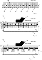
- Figures 1 to 3 show a transistor power switch device 100 of the kind described in US patent application publication US 2006-0145252 , comprising an array of base cells each comprising vertical insulated gate metal-oxide-silicon field-effect transistors ('MOSFET's) 108.
- a device of this kind is made with a high cell density, having several hundred-thousand or even several million cells per square centimeter of active semiconductor substrate, so as to reduce the on-state resistance, while avoiding comparable deterioration of the breakdown and unclamped inductive switching ('UIS') voltages.
- 'UIS' unclamped inductive switching
- the transistor power switch device 100 is an n-type device, although p-type devices are also possible.
- the transistor power switch device 100 comprises a semiconductor body formed from a substrate 101 of a first semiconductor type, in this example n-type, presenting opposite first and second faces 104 and 106.
- the transistor power switch device 100 further comprises an array of vertical transistor elements 108 which, in operation, carries current between said first and second faces 104,106.
- a drain electrode 112 contacts at the second face 106 an n-type drain region 102 formed in the substrate 101 which is shared by the transistor elements 108 and a source electrode 110 deposited on the first face 104 contacts the separate n-type source dopant regions 114 of the vertical transistor elements 108.
- the transistor elements 108 of the array comprise at the first face 104 an array of first current carrying transistor regions 114 of a first semiconductor type, in this example n-type source dopant regions, and at least one second current carrying transistor region of a second semiconductor type opposite to the first type, in this example a p-type region, interposed between the first semiconductor source regions and the second face 106.
- the second region in the substrate 101 comprises a lightly doped p-type high voltage ('PHV') body or well, region 122 and a more heavily doped p-type doped ('PSD') region 124 within the PHV region 122, together with boron protection implant ('BPI') regions 126 interposed between the PSD regions 124 and the source regions 114.
- the MOSFET base cells 108 may comprise second, body, regions which are separate from each other, in this example, the body regions merge together between and underneath the first, source regions 114 to form a single body region 122.
- the array of vertical MOSFET base cells 108 also comprises a gate electrode 116 for switchably controlling flow of said current in the body region 122.
- the gate electrodes are elements of a single gate electrode layer.
- the electrodes are not necessarily metallic but may be made of other conductive materials, such as polysilicon, for example.
- the drain region 102 of the substrate, the p regions 122,124,126 and the source regions 114 emerge at the face 104 of the substrate.
- the gate electrode 116 is insulated from the face 104 by an insulating layer 118 and the gate electrode 116 is insulated from the source electrode 110 by an insulating layer 120 with insulating spacers 121 insulating the edges of the gate electrode 116.
- the block consisting of the layers 118,116,120 is referred to as the "gate stack".
- the transistor power switch device 100 of US patent application publication US 2006-0145252 can provide a robust UIS immunity especially because the body regions are merged to provide a single PHV body region 122.
- a parasitic bipolar npn transistor can be activated.
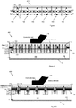
- Figures 4 to 6 illustrate an example of a transistor power switch device 400, in accordance with an example of an embodiment of the present invention.
- the source region 114 of each of the vertical transistor elements 108 contacting the conductive layer 110 comprises a plurality of arms at the first face 104.
- the arms extend, in this example from a common origin, radially towards an arm of a source region 114 of an adjacent vertical transistor element 108 of the array, the at least one body region 122, 124, 126 extend around and under the arms of the source regions 114 and, within each of the source regions, extend upwards (through the layer of the source region 114) to contact the conductive layer 110 at the first face 104 at a contact position 402 adjacent to an end of each of the arms of the source regions 114.
- the at least one body region 122, 124, 126 also extends upwards, within each of the source regions, (through the layer of the source region) to contact the conductive layer 110 at the first face 104 at a contact position 404 central to the source region 114 of the respective vertical transistor element 108.
- the transistor power switch device 400 has similarities to the device 100 but has PSD contacts 402 provided by the PSD region 124 emerging at the face 104 within the base cells at the ends of the arms of the base cells as well as at their centres 404, in this case providing four additional PSD contacts 402 to the source electrode 110.
- the gate stack and source region shapes are modified at the ends of the branches as illustrated in the Fig.4 .
- These additional PSD contacts increase the avalanche current capability that the FETs can withstand without activating parasitic bipolar npn transistors.
- the source region 114 of each of the vertical transistor elements 108 contacting the conductive layer 110 comprises a plurality of arms extending radially at the first face 104 towards an arm of a source region 114 of an adjacent vertical transistor element 108 of the array.
- the PHV body region 122 extends around and under the arms of the source regions 114.
- the PHV body region 122 is connected to the conductive layer 110 through the PSD regions 124 and the BPI regions 126, within each of the source regions, the BPI regions extend upwards, through the layers above the BPI regions, to contact the conductive layer 110 at the first face 104 at a PSD 124 contact position 402 adjacent to an end of each of the arms of the source regions 114 of the vertical transistor elements 108.
- the PHV body region 122 is also connected to the conductive layer 110 through the PSD regions 124 and the BPI regions 126, extending up within each of the source regions to contact the conductive layer 110 at the first face 104 at a contact position 404 central to each of the source regions 114 of the vertical transistor elements 108.
- the end of each of the arms of the source regions 114 is enlarged at the first face 104 around the contact position 402.
- the gate stack and the source regions 114 of the base MOSFET cells 108 are formed in the shape of crosses with elongate arms and enlarged rounded ends to the arms.
- the arms each have a smallest width at a position remote from the ends and at the enlarged rounded ends the arm has a position with a larger width than the smallest width. More in particular, in the shown example the arm has a maximum width at a location at the enlarged rounded ends.
- the second, body or well, region in the substrate 101 comprises a lightly doped p-type high voltage ('PHV') body region 122 and an array of more heavily doped p-type doped ('PSD') regions 124 within the PHV body region 122.
- the PHV region is formed, for example by diffusing dopant into the substrate from the face 104 after forming the gate layers 116, 118 and 120, using the gate stack as a mask to auto-align separate PHV regions of the base cells with the openings in the gate stack and then causing the dopant to spread a controlled distance vertically and laterally in the substrate so that the separate PHV regions of the base cells merge together between cells to form a continuous PHV body region 122.
- p-type dopant is blanket implanted in the openings in the gate stack at positions aligned with the future source regions 114 to form boron protection implant body regions ('BPI') 126 which will present a layer under the face of the source regions 114, the BPI regions emerging at the face 104 within the ends and centre of the source regions 114 of each base cell to prevent the punch through effect at the end of the arms.
- 'BPI' boron protection implant body regions
- the source regions 114 are formed after forming the merged PHV region.
- the source regions 114 may be formed by photo-masking circular PSD contact areas 402 in the enlarged ends and in a circular PSD contact area 404 in the centre of each of the cross-shaped gate layer openings of the base cells at the face 104 and implanting and diffusing n-type dopant into the substrate from the face 104 in the openings in the gate stack except in the circular PSD contact areas 402 and 404. Then the PSD body contact regions 124 are formed by implantation. The implanted n-type and p-type dopants are simultaneously activated by annealing.
- the source electrode 110 covers the array of MOSFET base cells 108 continuously, apart from an area for contact to the gate electrode 116, and makes electrical contact, through the openings in the gate stack 116-120, with the source regions 114 and also with the PHV region 124 through the BPI regions 126 at the contacts 402 and 404 and through the PSD regions 124 to ensure that there is no bias voltage to trigger the parasitic source-body-drain bipolar junction transistor structure even at the ends of the arms of the cross-shaped base cells.
- the gate electrode 116 overlaps the PHV body region 124 at the face 104 so that, in operation, a positive voltage applied to it relative to the source electrode 110 will create an inversion layer in the body region 122 forming a channel in the PHV region 122 at the face 104 under the gate electrode, the channel conducting the on current of the device when a positive voltage is applied to the drain electrode 112 relative to the source electrode 114.
- the on current flows up from the drain electrode 112 towards the face 104 adjacent the pn junction between the drain region 102 and the PHV body region 122 and then through the channels under the gate electrode to the source regions 114 of all the FETs 108.
- the gate electrode may be a single layer common to all the base cells 108 or may comprise more than one layer with suitable electrical connections.
- a contact (not shown in Figures 1 to 3 or 4 to 6 ) to the gate electrode may be present at an edge of the device 100 or 400.
- a contact to the drain electrode 112 may be made through the mounting of the device 100 or 400 to its casing (not shown in Figures 1 to 3 or 4 to 6 ).
- An electrical connection can made to the source electrode 110 by bonding an electrical connection lead 128 to the conductive layer of the source electrode 110 at a position directly over the MOSFETs 108.
- the electrical connection lead 128 is a bonding wire.
- the drain-source voltage reverse biases the p-n junctions between the PHV body region 122 and the drain region 102 in the substrate 101.
- the voltage increases, due to UIS for example, to a value at which the p-n junctions between the PHV body regions 122 and the drain region 102 exceed a threshold value, the p-n junctions break down due to the avalanche effect, as shown by the vertical arrows in Figures 2 , 5 and 6 .
- the electrical connections 402 of the PHV region 122 to the source electrode 110 through the PSD and BPI regions at the ends of the arms of the source regions 114 prevent the establishment of a voltage gradient along the arms of the source regions 114 in the PHV region 122 due to leakage currents, for example.
- the electrical connections 404 of the PHV region 122 to the source electrode 110 at the centres of the source regions contribute further to preventing such a voltage gradient.
- the avalanche current capability of switch device of Figures 4 to 6 is increased in the off state relative to the otherwise comparable device of Figures 1 to 3 .
- the gate stack is interposed between the source electrode 110 and the substrate 101 and limits the area of the source electrode 110 that is intimately in contact with the substrate 101. Not only does this limitation of contact area concentrate the flow of current, increasing the local current density and localising the generation of heat due to the flow of current through the electrically resistive material of the substrate, but in addition the electrical insulation of the gate stack is also a thermal insulation, limiting the capacity of the source electrode material to extract the heat generated.
- the heating effect is substantial, since the current flowing through the device 400 in UIS conditions can reach several hundred Amperes for a source-drain voltage of 30 V in one example.
- Figures 7 to 9 illustrate a transistor power switch device 700 in accordance with an example of an embodiment of the invention, comprising an array of vertical insulated gate metal-oxide-silicon field-effect transistors ('MOSFET's) 108 similar to the transistors of Figures 4 to 6 .
- the device 700 includes a reverse biased vertical avalanche diode 702 in the semiconductor body 101 electrically in parallel with the array of transistors 108 for conducting breakdown current between the faces 104 and 106 of the device 700 in the off state of the device, the diode 702 having a first current carrying region 704 in contact with the conductive source electrode layer 110, and a second semiconductor region 706 which is electrically connected with the second face 106 and which is situated under the first current carrying region 704.
- 'MOSFET's vertical insulated gate metal-oxide-silicon field-effect transistors
- the first current carrying region 704 of the repetitive avalanche diode 702 is of the same second conductivity type as the p regions 122 to 126 of the MOSFETs 108, and the second semiconductor region 706 is of the same first conductivity type as the drain regions 102 of the MOSFETs 108, in this example n-type.
- the gate 116 is biased positively relative to the source electrode 110 by a voltage slightly greater than the threshold voltage Vth of the MOSFETs 108 and the drain electrode is biased positively relative to the source electrode 110, the repetitive avalanche diode 702 being reverse biased in this condition.
- the current passes first vertically up from the drain electrode 112 in the drain region 102 towards the face 104 at the perimeters of the PHV body regions 122 then laterally through the channel under the gate electrode in the PHV region 122 at the perimeters of the source regions 114 of the MOSFETs 108.
- avalanche current through the diode 702 passes first vertically through the second current carrying region 706 in the substrate 101, then through the layers of the first current carrying region 704, presenting a short current conduction path, as shown by the thick arrows in Figures 8 and 9 , minimising heat generation.
- Avalanche current in the MOSFETs 108 also passes vertically, through the p regions 122, 124 and 126, but is restricted to an aggregate area at the face 104 less than the total area of the array of MOSFETs 108 by the interposed gate stack 116 to 120, as shown by the thin arrows in Figures 8 and 9 .
- the conductive source electrode layer 110 covers the avalanche diode 702 as well as the MOSFETs 108 and electrical and thermal contact of the first current carrying region 704 with the conductive electrode layer 110 is continuous over substantially the whole area of the first current carrying region 704 of the diode 702 at the face 104, unimpeded by any layer of insulator material.
- the avalanche diode 702 is dimensioned to withstand repetitive avalanche currents and will be referred to hereinafter as a repetitive avalanche diode 702. Accordingly, current density is minimised and evacuation through the source electrode 110 of heat generated in the diode 702 by the current is maximised.
- the first current carrying region 704 of the diode 702 comprises a lightly doped p-type PHV body region 708, a more heavily doped PSD region 710 within the PHV region 708 and a BPI region 712 extending from the PSD region 710 to the face 104 and contacting the source electrode 110.
- the PHV body region 708, the PSD region 710 and the BPI region 712 are formed simultaneously with the manufacturing steps of the PHV body region 122, the PSD region 124 and the BPI region 126 of the MOSFETs 108, using appropriate masking.
- Figure 10 shows an example of the equivalent electrical circuit 1000 of the device 700, illustrating one out of a total of M MOSFET base cells and one out of a total of N repetitive avalanche diodes.
- a node 1002 represents the n-type side of the p-n junction between the NSD source region 114 of the MOSFET 108 and the PHV body region 122, the p-type side being represented by a node 1004 and the p-n junction by a diode 1006.
- a resistor Rsource represents the resistance of the material of the source region 114 in series between the node 1002 and the source electrode 110.
- a node 1008 represents the n-type side of the p-n junction between the n-type drain region 102 of the MOSFETs 108 and the PHV body region 122, the p-type side being represented by the node 1004 and the p-n junction by a diode 1010.
- a resistor Rdrain represents the resistance of the material of the drain region 102 in series between the node 1008 and the drain electrode 112.
- a resistor Rbulk represents the resistance of the material of the PHV, PSD and BPI p regions 122, 124 and 126 in series between the p-type sides of the p-n junctions represented by diodes 1004 and 1010 and the connection with the source electrode 110.
- the repetitive avalanche diode 702 is connected electrically in parallel with the array of transistors 108 for conducting breakdown current in the off state of the device between the drain electrode 112 and the source electrode 110 at the second and first faces 106 and 104 respectively.
- the p-n junction between the n-type region 706 of the repetitive avalanche diode 702 and its p-type region 704 is represented by a diode 1012, the n-type side being connected to the node 1008.
- a resistor 1014 represents the resistance of the material of the p region 704 in series between the p-type side of the p-n junction represented by diode 1012 and the connection with the source electrode 110.
- the p region 704 forms a first current carrying region in contact with the conductive source electrode layer 110 and the n-type region 706 of the repetitive avalanche diode 702 forms a second semiconductor region electrically connected with the drain electrode 112 at the second face 106.
- the electrical connection lead 128 is bonded to the conductive layer of the source electrode 110 at a position over the first current carrying region 704 of the repetitive avalanche diode 702, as shown in Figures 8 and 9 .
- the electrical connection lead 128 comprises a wire extending away from the conductive layer of the source electrode 110 so as to dissipate heat from the diode 702.
- the repetitive avalanche diode 702 which has a breakdown voltage less than vertical MOSFETs 108 but as the avalanche current continues, the repetitive avalanche diode 702 increases in temperature, its breakdown voltage increases and the MOSFETs 108 participate to a greater extent in conducting avalanche current between the drain and source electrodes 112 and 110.
- the area of the diode 702 and, more specifically, the area of its p region 704 at the first face 104 and contacting the source electrode conductive layer 110 is adapted to the diameter of the connection lead and the length of the bond to the contact and is several orders of magnitude greater than areas of the individual MOSFETs 108.
- an individual MOSFET base cell 108 measures 50 to 100 ⁇ m 2 and the electrical connection lead wire 128 is approximately 250 to 380 ⁇ m diameter, whereas the diode 702 measures 500 000 ⁇ m 2 .
- the device 700 comprises, in the semiconductor body 101 on a single die, a plurality of the reverse biased repetitive avalanche diodes 702 each of which is surrounded by one or more arrays of MOSFET cells.
- Figure 11 shows an example of a device 1100 of this kind, comprising fourteen diodes 702.
- the device 1100 comprises ten diodes 702 and six hundred thousand MOSFET cells 108.
- the device 1200 comprises a respective wire electrical connection lead 128 bonded to the conductive layer of the source electrode 110 at a position 1202 over the first current carrying regions 704 of each of the repetitive avalanche diodes 702.
- a single wire electrical connection lead 128 is bonded to the conductive layer of the source electrode 110 at a position over each of the repetitive avalanche diodes.
- the device 1300 comprises one or more of the wire electrical connection leads 128 bonded to the conductive layer of the source electrode 110 at a plurality of positions 1302 over the first current carrying regions of more than one of the repetitive avalanche diodes 702.
- the same wire electrical connection lead 128 is bonded over two of the repetitive avalanche diodes 702.
- electrically conductive contact bumps are grown on the source electrode 110 over the repetitive avalanche diodes 702 and then contacted by connections 128.
- Various electrical connection materials can be used over the conductive layer of the source electrode 110 such as aluminium ribbon, copper stud, gold or solder bumps.
- Figure 14 shows a comparison of the results of UIS repetitive avalanche tests on a transistor power switch device 400 of the kind illustrated in Figures 4 to 6 , illustrated by the dotted line 1400 with the results of a similar test on a transistor power switch device 700 of the kind illustrated in Figures 7 to 9 of the same die size and similar manufacturing process, illustrated by the full line 1402.
- An improvement of a factor of ten in the robustness of the device is obtained. It will be appreciated that using a part of the die area for the diodes 702 reduces the die area available for the MOSFETs 108, which could increase the on-resistance Rdson of the switching device 700 compared to that of the device 400.
- the improvement in UIS robustness of the device 700 compared to that of the device 400 enables its various operating characteristics to be adjusted to a different compromise, compensating the increase in Rdson.
- connections may be any type of connection suitable to transfer signals from or to the respective nodes, units or devices, for example via intermediate devices. Accordingly, unless implied or stated otherwise the connections may for example be direct connections or indirect connections.
- the semiconductor substrate described herein can be any semiconductor material or combinations of materials, such as gallium arsenide, silicon germanium, silicon-on-insulator (SOI), silicon, mono-crystalline silicon, the like, and combinations of the above.
- SOI silicon-on-insulator
- illustrated hardware elements may be circuitry located on a single integrated circuit or within a same device or may include a plurality of separate integrated circuits or separate devices interconnected with each other. Also, hardware elements in an embodiment of the invention may be replaced by software or code representations in an embodiment of the invention.
Landscapes
- Insulated Gate Type Field-Effect Transistor (AREA)
- Metal-Oxide And Bipolar Metal-Oxide Semiconductor Integrated Circuits (AREA)
- Semiconductor Integrated Circuits (AREA)
Claims (11)
- Eine Transistor Leistungsschalter Vorrichtung (400, 700) aufweisend
einen Halbleiterkörper (101), welcher eine gegenüberliegende erste und zweite Fläche (104, 106) präsentiert,
wobei die Schalter Vorrichtung aufweist einen Array von vertikalen Feldeffekt Transistorelementen (108) zum Leiten von Strom zwischen der ersten und zweiten Fläche (104, 106),
wobei der Array von Transistorelementen (108) aufweist bei der ersten Fläche (104) einen Array von Sourceregionen (114) von einem ersten Halbleitertyp,
wobei zumindest eine Körperregion (122, 124, 126) von einem zweiten Halbleitertyp gegenüberliegend zu dem ersten Typ ist, welcher eingeschoben ist zwischen die Sourceregionen (114) und die zweiter Fläche (106),
wobei zumindest eine Drainregion (102) von dem ersten Halbleitertyp elektrisch verbunden ist mit der zweiten Fläche (106), und
wobei zumindest eine Steuerelektrode (116) zum schaltbaren Steuern ist von Fluss von dem Strom durch die zumindest eine Körperregion (122, 124, 126), und
wobei eine leitfähige Schicht (110) die Sourceregion (114) kontaktiert und isoliert ist von der Steuerelektrode (116) mittels zumindest einer isolierenden Schicht (120, 121),
wobei die Sourceregion (114) von jedem der vertikalen Transistorelementen (108) kontaktierend die leitfähige Schicht (110) ausgebildet ist in der Form von einem Kreuz und aufweist eine Mehrzahl von Armen, welche sich erstrecken radial über die erste Fläche (104) zu einem Arm von einer Sourecregion (114) von einem danebenliegenden vertikalen Transistorelement (108) von dem Array,
wobei zumindest eine Körperregion (122, 124, 126) sich erstreckt um und unter den Armen von den Sourceregionen (114) und ineinander übergeht zwischen den vertikalen Transistorelementen (108) zum Ausbilden einer kontinuierlichen Körperregion, und
wobei die zumindest eine Körperregion (122, 124, 126) sich erstreckt hinauf in jede von den Sourceregionen zum Kontaktieren der leitfähigen Schicht (110) bei der ersten Fläche (104), dadurch gekennzeichnet, dass die zumindest eine Körperregion (122, 124, 126) kontaktiert die leitfähige Schicht (110) bei Kontaktpositionen (402),
wobei jede Kontaktposition (402) danebenliegend ist zu einem Ende von jedem der Arme von den Sourceregionen (114). - Eine Transistor Leistungsschalter Vorrichtung wie in Anspruch 1 beansprucht,
wobei die zumindest eine Körperregion (122, 124, 126) zusätzlich sich erstreckt hinauf in jede der Sourceregionen zum Kontaktieren der leitfähigen Schicht (110) bei der ersten Fläche (104) bei einer Kontaktposition (404), welche zentral ist zu jeder von den Sourceregionen (114) von den vertikalen Transistorelementen (108). - Eine Transistor Leistungsschalter Vorrichtung wie in Anspruch 1 oder 2 beansprucht, wobei das Ende von jedem von den Armen von den Sourceregionen (114) erweitert ist bei der ersten Fläche (104) herum um die Kontaktposition (114).
- Eine Transistor Leistungsschalter Vorrichtung wie in irgendeinem vorherigen Anspruch beansprucht, wobei die Schalter Vorrichtung zusätzlich aufweist zumindest eine reverse vorgepolte vertikale Avalanchediode (702) in dem Halbleiterkörper (101), welcher elektrisch verbunden ist parallel mit dem Array von Transistoren (108) zum Leiten von Durchbruchstrom zwischen der ersten und der zweiten Fläche (104, 106) in dem Aus-Zustand von der Vorrichtung und aufweisend eine ersten stromleitende Dioderegion (704) von dem zweiten Halbleitertyp in Kontakt mit der ersten Fläche (104) und mit der leitfähigen Schicht (110) und eine zweite Halbleiterregion (706) von dem ersten Halbleitertyp, welcher elektrisch verbunden sind mit der zweiten Fläche (106).
- Eine Transistor Leistungsschalter Vorrichtung wie in Anspruch 4 beansprucht, und beinhaltend eine elektrische Verbindungsleitung (128), welche verbunden ist zu der leitfähigen Schicht (110), bei einer Position über die erste stromleitende Diodenregion (704).
- Eine Transistor Leistungsschalter Vorrichtung wie in Anspruch 5 beansprucht, wobei die elektrische Verbindungsleitung (128) aufweist ein Kabel, welches sich erstreckt weg von der leitfähigen Schicht (110), um zu Dissipieren Wärme von der Diode (702).
- Eine Transistor Leistungsschalter Vorrichtung wie in Anspruch 5 beansprucht, wobei die elektrische Verbindungsleitung (128) aufweist einen Kontakterhebung oben auf der leitfähigen Schicht (110), um zu Dissipieren Wärme von der Diode (402).
- Eine Transistor Leistungsschalter Vorrichtung wie in Anspruch 5 oder 6 beansprucht, und beinhaltend
in dem Halbleiterkörper (101) eine Mehrzahl von reversen vorgepolten Avalanchedioden (702),
wobei zumindest eine von den elektrischen Verbindungsleitungen (128) verbunden ist zu der leitfähigen Schicht (110) über die ersten stromleitenden Diodenregionen (704) von jeder von den Avalanchedioden (702). - Eine Transistor Leistungsschalter Vorrichtung wie in Anspruch 7 beansprucht, wobei zumindest eine von den elektrischen Verbindungsleitungen (128) verbunden ist zu der leitfähigen Schicht (110) bei einer Mehrzahl von Positionen über die ersten stromleitenden Dioderegionen (704) von mehr als einer von den Avalanchedioden (702).
- Eine Transistor Leistungsschalter Vorrichtung wie in irgendeinem der Ansprüche 4 bis 9 beansprucht, wobei die ersten stromleitende Transistorregionen (114) jeweils die leitfähige Schicht (110) über einen Bereich kontaktiert, welcher im Wesentlichen niedriger ist als ein Bereich, über welchen die erste stromleitende Dioderegion (704) von der reversen vorgepolten Avalanchediode (702) die leitfähige Schicht (110) kontaktiert.
- Eine Transistor Leistungsschalter Vorrichtung wie in irgendeinem der Ansprüche 4 bis 10 beansprucht, wobei die reverse vorgepolte Avalanchediode (702) eine Durchbruchspannung hat, welche niedriger ist als die vertikalen Transistorelemente von dem Array.
Applications Claiming Priority (1)
| Application Number | Priority Date | Filing Date | Title |
|---|---|---|---|
| PCT/IB2008/055656 WO2010061245A1 (en) | 2008-11-27 | 2008-11-27 | Power mos transistor device |
Publications (2)
| Publication Number | Publication Date |
|---|---|
| EP2371003A1 EP2371003A1 (de) | 2011-10-05 |
| EP2371003B1 true EP2371003B1 (de) | 2018-07-04 |
Family
ID=40651650
Family Applications (1)
| Application Number | Title | Priority Date | Filing Date |
|---|---|---|---|
| EP08875951.9A Active EP2371003B1 (de) | 2008-11-27 | 2008-11-27 | Leistungs-mos-transistoranordnung |
Country Status (4)
| Country | Link |
|---|---|
| US (1) | US8604560B2 (de) |
| EP (1) | EP2371003B1 (de) |
| TW (1) | TWI521692B (de) |
| WO (1) | WO2010061245A1 (de) |
Families Citing this family (3)
| Publication number | Priority date | Publication date | Assignee | Title |
|---|---|---|---|---|
| WO2010061244A1 (en) * | 2008-11-27 | 2010-06-03 | Freescale Semiconductor, Inc. | Power mos transistor device and switch apparatus comprising the same |
| CN102473724B (zh) | 2009-08-18 | 2015-02-18 | 飞思卡尔半导体公司 | 晶体管功率开关器件及测量其特性的方法 |
| DE102015112502B4 (de) * | 2015-07-30 | 2021-11-04 | Infineon Technologies Ag | Halbleiterbauelemente |
Family Cites Families (9)
| Publication number | Priority date | Publication date | Assignee | Title |
|---|---|---|---|---|
| JPS6180860A (ja) | 1984-09-28 | 1986-04-24 | Hitachi Ltd | パワ−mosfet |
| JP2572210B2 (ja) | 1984-11-20 | 1997-01-16 | 三菱電機株式会社 | 縦型パワ−mos電界効果型半導体装置 |
| JPS62235785A (ja) | 1986-04-07 | 1987-10-15 | Nec Corp | 縦型電界効果トランジスタ |
| JP4666708B2 (ja) | 1999-10-13 | 2011-04-06 | 新電元工業株式会社 | 電界効果トランジスタ |
| FR2833776B1 (fr) | 2001-10-09 | 2005-09-09 | Valeo Equip Electr Moteur | Alternateur a pont de redressement, notamment pour vehicule automobile |
| EP1387408A1 (de) | 2002-06-12 | 2004-02-04 | Motorola, Inc. | Leistungshalbleiteranordnung und Verfahren zu deren Herstellung |
| JP4167294B2 (ja) | 2005-07-26 | 2008-10-15 | 松下電器産業株式会社 | 半導体素子及び電気機器 |
| US7667265B2 (en) | 2006-01-30 | 2010-02-23 | Fairchild Semiconductor Corporation | Varying mesa dimensions in high cell density trench MOSFET |
| WO2010061244A1 (en) | 2008-11-27 | 2010-06-03 | Freescale Semiconductor, Inc. | Power mos transistor device and switch apparatus comprising the same |
-
2008
- 2008-11-27 US US13/129,516 patent/US8604560B2/en active Active
- 2008-11-27 EP EP08875951.9A patent/EP2371003B1/de active Active
- 2008-11-27 WO PCT/IB2008/055656 patent/WO2010061245A1/en not_active Ceased
-
2009
- 2009-11-27 TW TW098140693A patent/TWI521692B/zh active
Non-Patent Citations (1)
| Title |
|---|
| None * |
Also Published As
| Publication number | Publication date |
|---|---|
| TWI521692B (zh) | 2016-02-11 |
| US8604560B2 (en) | 2013-12-10 |
| EP2371003A1 (de) | 2011-10-05 |
| TW201030969A (en) | 2010-08-16 |
| US20110227146A1 (en) | 2011-09-22 |
| WO2010061245A1 (en) | 2010-06-03 |
Similar Documents
| Publication | Publication Date | Title |
|---|---|---|
| US7902604B2 (en) | Configuration of gate to drain (GD) clamp and ESD protection circuit for power device breakdown protection | |
| US10249759B2 (en) | Connection arrangements for integrated lateral diffusion field effect transistors | |
| EP3249815B1 (de) | Schaltungsanordnung zum schnellen abschalten einer bidirektionalen schaltvorrichtung | |
| US8482031B2 (en) | Lateral insulated gate bipolar transistors (LIGBTS) | |
| US10957686B2 (en) | Semiconductor device including an integrated resistor and method of producing thereof | |
| JP4185157B2 (ja) | 半導体素子及び電気機器 | |
| CN111201611B (zh) | 具有高dv/dt能力的功率开关装置及制造这种装置的方法 | |
| US20220278027A1 (en) | Connection arrangements for integrated lateral diffusion field effect transistors having a backside contact | |
| US9620498B2 (en) | Configuration of gate to drain (GD) clamp and ESD protection circuit for power device breakdown protection | |
| US8530953B2 (en) | Power MOS transistor device and switch apparatus comprising the same | |
| CN109643728A (zh) | 半导体装置 | |
| KR102832585B1 (ko) | 센서 소자를 갖는 넓은 밴드갭 반도체 디바이스 | |
| EP2371003B1 (de) | Leistungs-mos-transistoranordnung | |
| CN104253152A (zh) | 一种igbt及其制造方法 | |
| EP3016142A1 (de) | Igbt mit eingebauter diode und herstellungsverfahren dafür | |
| US11482615B2 (en) | Super-junction power MOSFET device with improved ruggedness, and method of manufacturing | |
| US20260104295A1 (en) | Circuitry for allowing multiple sensors on a semiconductor die to share a common sensor pad |
Legal Events
| Date | Code | Title | Description |
|---|---|---|---|
| PUAI | Public reference made under article 153(3) epc to a published international application that has entered the european phase |
Free format text: ORIGINAL CODE: 0009012 |
|
| 17P | Request for examination filed |
Effective date: 20110627 |
|
| AK | Designated contracting states |
Kind code of ref document: A1 Designated state(s): AT BE BG CH CY CZ DE DK EE ES FI FR GB GR HR HU IE IS IT LI LT LU LV MC MT NL NO PL PT RO SE SI SK TR |
|
| DAX | Request for extension of the european patent (deleted) | ||
| RAP1 | Party data changed (applicant data changed or rights of an application transferred) |
Owner name: NXP USA, INC. |
|
| 17Q | First examination report despatched |
Effective date: 20170216 |
|
| GRAP | Despatch of communication of intention to grant a patent |
Free format text: ORIGINAL CODE: EPIDOSNIGR1 |
|
| INTG | Intention to grant announced |
Effective date: 20180406 |
|
| GRAS | Grant fee paid |
Free format text: ORIGINAL CODE: EPIDOSNIGR3 |
|
| GRAA | (expected) grant |
Free format text: ORIGINAL CODE: 0009210 |
|
| AK | Designated contracting states |
Kind code of ref document: B1 Designated state(s): AT BE BG CH CY CZ DE DK EE ES FI FR GB GR HR HU IE IS IT LI LT LU LV MC MT NL NO PL PT RO SE SI SK TR |
|
| REG | Reference to a national code |
Ref country code: GB Ref legal event code: FG4D |
|
| REG | Reference to a national code |
Ref country code: CH Ref legal event code: EP |
|
| REG | Reference to a national code |
Ref country code: AT Ref legal event code: REF Ref document number: 1015434 Country of ref document: AT Kind code of ref document: T Effective date: 20180715 |
|
| REG | Reference to a national code |
Ref country code: IE Ref legal event code: FG4D |
|
| REG | Reference to a national code |
Ref country code: DE Ref legal event code: R096 Ref document number: 602008055895 Country of ref document: DE |
|
| REG | Reference to a national code |
Ref country code: NL Ref legal event code: MP Effective date: 20180704 |
|
| REG | Reference to a national code |
Ref country code: LT Ref legal event code: MG4D |
|
| REG | Reference to a national code |
Ref country code: AT Ref legal event code: MK05 Ref document number: 1015434 Country of ref document: AT Kind code of ref document: T Effective date: 20180704 |
|
| PG25 | Lapsed in a contracting state [announced via postgrant information from national office to epo] |
Ref country code: NL Free format text: LAPSE BECAUSE OF FAILURE TO SUBMIT A TRANSLATION OF THE DESCRIPTION OR TO PAY THE FEE WITHIN THE PRESCRIBED TIME-LIMIT Effective date: 20180704 |
|
| PG25 | Lapsed in a contracting state [announced via postgrant information from national office to epo] |
Ref country code: PL Free format text: LAPSE BECAUSE OF FAILURE TO SUBMIT A TRANSLATION OF THE DESCRIPTION OR TO PAY THE FEE WITHIN THE PRESCRIBED TIME-LIMIT Effective date: 20180704 Ref country code: LT Free format text: LAPSE BECAUSE OF FAILURE TO SUBMIT A TRANSLATION OF THE DESCRIPTION OR TO PAY THE FEE WITHIN THE PRESCRIBED TIME-LIMIT Effective date: 20180704 Ref country code: AT Free format text: LAPSE BECAUSE OF FAILURE TO SUBMIT A TRANSLATION OF THE DESCRIPTION OR TO PAY THE FEE WITHIN THE PRESCRIBED TIME-LIMIT Effective date: 20180704 Ref country code: IS Free format text: LAPSE BECAUSE OF FAILURE TO SUBMIT A TRANSLATION OF THE DESCRIPTION OR TO PAY THE FEE WITHIN THE PRESCRIBED TIME-LIMIT Effective date: 20181104 Ref country code: BG Free format text: LAPSE BECAUSE OF FAILURE TO SUBMIT A TRANSLATION OF THE DESCRIPTION OR TO PAY THE FEE WITHIN THE PRESCRIBED TIME-LIMIT Effective date: 20181004 Ref country code: CZ Free format text: LAPSE BECAUSE OF FAILURE TO SUBMIT A TRANSLATION OF THE DESCRIPTION OR TO PAY THE FEE WITHIN THE PRESCRIBED TIME-LIMIT Effective date: 20180704 Ref country code: NO Free format text: LAPSE BECAUSE OF FAILURE TO SUBMIT A TRANSLATION OF THE DESCRIPTION OR TO PAY THE FEE WITHIN THE PRESCRIBED TIME-LIMIT Effective date: 20181004 Ref country code: SE Free format text: LAPSE BECAUSE OF FAILURE TO SUBMIT A TRANSLATION OF THE DESCRIPTION OR TO PAY THE FEE WITHIN THE PRESCRIBED TIME-LIMIT Effective date: 20180704 Ref country code: GR Free format text: LAPSE BECAUSE OF FAILURE TO SUBMIT A TRANSLATION OF THE DESCRIPTION OR TO PAY THE FEE WITHIN THE PRESCRIBED TIME-LIMIT Effective date: 20181005 Ref country code: FI Free format text: LAPSE BECAUSE OF FAILURE TO SUBMIT A TRANSLATION OF THE DESCRIPTION OR TO PAY THE FEE WITHIN THE PRESCRIBED TIME-LIMIT Effective date: 20180704 |
|
| PG25 | Lapsed in a contracting state [announced via postgrant information from national office to epo] |
Ref country code: HR Free format text: LAPSE BECAUSE OF FAILURE TO SUBMIT A TRANSLATION OF THE DESCRIPTION OR TO PAY THE FEE WITHIN THE PRESCRIBED TIME-LIMIT Effective date: 20180704 Ref country code: ES Free format text: LAPSE BECAUSE OF FAILURE TO SUBMIT A TRANSLATION OF THE DESCRIPTION OR TO PAY THE FEE WITHIN THE PRESCRIBED TIME-LIMIT Effective date: 20180704 Ref country code: LV Free format text: LAPSE BECAUSE OF FAILURE TO SUBMIT A TRANSLATION OF THE DESCRIPTION OR TO PAY THE FEE WITHIN THE PRESCRIBED TIME-LIMIT Effective date: 20180704 |
|
| REG | Reference to a national code |
Ref country code: DE Ref legal event code: R097 Ref document number: 602008055895 Country of ref document: DE |
|
| PG25 | Lapsed in a contracting state [announced via postgrant information from national office to epo] |
Ref country code: IT Free format text: LAPSE BECAUSE OF FAILURE TO SUBMIT A TRANSLATION OF THE DESCRIPTION OR TO PAY THE FEE WITHIN THE PRESCRIBED TIME-LIMIT Effective date: 20180704 Ref country code: RO Free format text: LAPSE BECAUSE OF FAILURE TO SUBMIT A TRANSLATION OF THE DESCRIPTION OR TO PAY THE FEE WITHIN THE PRESCRIBED TIME-LIMIT Effective date: 20180704 Ref country code: EE Free format text: LAPSE BECAUSE OF FAILURE TO SUBMIT A TRANSLATION OF THE DESCRIPTION OR TO PAY THE FEE WITHIN THE PRESCRIBED TIME-LIMIT Effective date: 20180704 |
|
| PLBE | No opposition filed within time limit |
Free format text: ORIGINAL CODE: 0009261 |
|
| STAA | Information on the status of an ep patent application or granted ep patent |
Free format text: STATUS: NO OPPOSITION FILED WITHIN TIME LIMIT |
|
| PG25 | Lapsed in a contracting state [announced via postgrant information from national office to epo] |
Ref country code: DK Free format text: LAPSE BECAUSE OF FAILURE TO SUBMIT A TRANSLATION OF THE DESCRIPTION OR TO PAY THE FEE WITHIN THE PRESCRIBED TIME-LIMIT Effective date: 20180704 Ref country code: SK Free format text: LAPSE BECAUSE OF FAILURE TO SUBMIT A TRANSLATION OF THE DESCRIPTION OR TO PAY THE FEE WITHIN THE PRESCRIBED TIME-LIMIT Effective date: 20180704 |
|
| 26N | No opposition filed |
Effective date: 20190405 |
|
| REG | Reference to a national code |
Ref country code: CH Ref legal event code: PL |
|
| GBPC | Gb: european patent ceased through non-payment of renewal fee |
Effective date: 20181127 |
|
| PG25 | Lapsed in a contracting state [announced via postgrant information from national office to epo] |
Ref country code: MC Free format text: LAPSE BECAUSE OF FAILURE TO SUBMIT A TRANSLATION OF THE DESCRIPTION OR TO PAY THE FEE WITHIN THE PRESCRIBED TIME-LIMIT Effective date: 20180704 Ref country code: LU Free format text: LAPSE BECAUSE OF NON-PAYMENT OF DUE FEES Effective date: 20181127 |
|
| REG | Reference to a national code |
Ref country code: BE Ref legal event code: MM Effective date: 20181130 |
|
| REG | Reference to a national code |
Ref country code: IE Ref legal event code: MM4A |
|
| PG25 | Lapsed in a contracting state [announced via postgrant information from national office to epo] |
Ref country code: LI Free format text: LAPSE BECAUSE OF NON-PAYMENT OF DUE FEES Effective date: 20181130 Ref country code: CH Free format text: LAPSE BECAUSE OF NON-PAYMENT OF DUE FEES Effective date: 20181130 Ref country code: SI Free format text: LAPSE BECAUSE OF FAILURE TO SUBMIT A TRANSLATION OF THE DESCRIPTION OR TO PAY THE FEE WITHIN THE PRESCRIBED TIME-LIMIT Effective date: 20180704 |
|
| PG25 | Lapsed in a contracting state [announced via postgrant information from national office to epo] |
Ref country code: IE Free format text: LAPSE BECAUSE OF NON-PAYMENT OF DUE FEES Effective date: 20181127 Ref country code: FR Free format text: LAPSE BECAUSE OF NON-PAYMENT OF DUE FEES Effective date: 20181130 |
|
| PG25 | Lapsed in a contracting state [announced via postgrant information from national office to epo] |
Ref country code: BE Free format text: LAPSE BECAUSE OF NON-PAYMENT OF DUE FEES Effective date: 20181130 |
|
| PG25 | Lapsed in a contracting state [announced via postgrant information from national office to epo] |
Ref country code: GB Free format text: LAPSE BECAUSE OF NON-PAYMENT OF DUE FEES Effective date: 20181127 |
|
| PG25 | Lapsed in a contracting state [announced via postgrant information from national office to epo] |
Ref country code: MT Free format text: LAPSE BECAUSE OF NON-PAYMENT OF DUE FEES Effective date: 20181127 |
|
| PG25 | Lapsed in a contracting state [announced via postgrant information from national office to epo] |
Ref country code: TR Free format text: LAPSE BECAUSE OF FAILURE TO SUBMIT A TRANSLATION OF THE DESCRIPTION OR TO PAY THE FEE WITHIN THE PRESCRIBED TIME-LIMIT Effective date: 20180704 |
|
| PG25 | Lapsed in a contracting state [announced via postgrant information from national office to epo] |
Ref country code: PT Free format text: LAPSE BECAUSE OF FAILURE TO SUBMIT A TRANSLATION OF THE DESCRIPTION OR TO PAY THE FEE WITHIN THE PRESCRIBED TIME-LIMIT Effective date: 20180704 |
|
| PG25 | Lapsed in a contracting state [announced via postgrant information from national office to epo] |
Ref country code: HU Free format text: LAPSE BECAUSE OF FAILURE TO SUBMIT A TRANSLATION OF THE DESCRIPTION OR TO PAY THE FEE WITHIN THE PRESCRIBED TIME-LIMIT; INVALID AB INITIO Effective date: 20081127 Ref country code: CY Free format text: LAPSE BECAUSE OF FAILURE TO SUBMIT A TRANSLATION OF THE DESCRIPTION OR TO PAY THE FEE WITHIN THE PRESCRIBED TIME-LIMIT Effective date: 20180704 |
|
| P01 | Opt-out of the competence of the unified patent court (upc) registered |
Effective date: 20230725 |
|
| REG | Reference to a national code |
Ref country code: DE Ref legal event code: R079 Ref document number: 602008055895 Country of ref document: DE Free format text: PREVIOUS MAIN CLASS: H01L0029780000 Ipc: H10D0030600000 |
|
| PGFP | Annual fee paid to national office [announced via postgrant information from national office to epo] |
Ref country code: DE Payment date: 20251022 Year of fee payment: 18 |