EP2369733A2 - Circuit assembly and method for generating alternating current from a number of power supply units with output DC voltage which varies over time - Google Patents
Circuit assembly and method for generating alternating current from a number of power supply units with output DC voltage which varies over time Download PDFInfo
- Publication number
- EP2369733A2 EP2369733A2 EP11151095A EP11151095A EP2369733A2 EP 2369733 A2 EP2369733 A2 EP 2369733A2 EP 11151095 A EP11151095 A EP 11151095A EP 11151095 A EP11151095 A EP 11151095A EP 2369733 A2 EP2369733 A2 EP 2369733A2
- Authority
- EP
- European Patent Office
- Prior art keywords
- circuit
- voltage
- arrangement according
- converter
- positive
- Prior art date
- Legal status (The legal status is an assumption and is not a legal conclusion. Google has not performed a legal analysis and makes no representation as to the accuracy of the status listed.)
- Granted
Links
Images


Classifications
-
- H—ELECTRICITY
- H02—GENERATION; CONVERSION OR DISTRIBUTION OF ELECTRIC POWER
- H02M—APPARATUS FOR CONVERSION BETWEEN AC AND AC, BETWEEN AC AND DC, OR BETWEEN DC AND DC, AND FOR USE WITH MAINS OR SIMILAR POWER SUPPLY SYSTEMS; CONVERSION OF DC OR AC INPUT POWER INTO SURGE OUTPUT POWER; CONTROL OR REGULATION THEREOF
- H02M7/00—Conversion of ac power input into dc power output; Conversion of dc power input into ac power output
- H02M7/42—Conversion of dc power input into ac power output without possibility of reversal
- H02M7/44—Conversion of dc power input into ac power output without possibility of reversal by static converters
- H02M7/48—Conversion of dc power input into ac power output without possibility of reversal by static converters using discharge tubes with control electrode or semiconductor devices with control electrode
- H02M7/53—Conversion of dc power input into ac power output without possibility of reversal by static converters using discharge tubes with control electrode or semiconductor devices with control electrode using devices of a triode or transistor type requiring continuous application of a control signal
- H02M7/537—Conversion of dc power input into ac power output without possibility of reversal by static converters using discharge tubes with control electrode or semiconductor devices with control electrode using devices of a triode or transistor type requiring continuous application of a control signal using semiconductor devices only, e.g. single switched pulse inverters
-
- H—ELECTRICITY
- H02—GENERATION; CONVERSION OR DISTRIBUTION OF ELECTRIC POWER
- H02J—CIRCUIT ARRANGEMENTS OR SYSTEMS FOR SUPPLYING OR DISTRIBUTING ELECTRIC POWER; SYSTEMS FOR STORING ELECTRIC ENERGY
- H02J7/00—Circuit arrangements for charging or depolarising batteries or for supplying loads from batteries
- H02J7/34—Parallel operation in networks using both storage and other dc sources, e.g. providing buffering
- H02J7/35—Parallel operation in networks using both storage and other dc sources, e.g. providing buffering with light sensitive cells
-
- H—ELECTRICITY
- H02—GENERATION; CONVERSION OR DISTRIBUTION OF ELECTRIC POWER
- H02M—APPARATUS FOR CONVERSION BETWEEN AC AND AC, BETWEEN AC AND DC, OR BETWEEN DC AND DC, AND FOR USE WITH MAINS OR SIMILAR POWER SUPPLY SYSTEMS; CONVERSION OF DC OR AC INPUT POWER INTO SURGE OUTPUT POWER; CONTROL OR REGULATION THEREOF
- H02M7/00—Conversion of ac power input into dc power output; Conversion of dc power input into ac power output
- H02M7/42—Conversion of dc power input into ac power output without possibility of reversal
- H02M7/44—Conversion of dc power input into ac power output without possibility of reversal by static converters
- H02M7/48—Conversion of dc power input into ac power output without possibility of reversal by static converters using discharge tubes with control electrode or semiconductor devices with control electrode
-
- H—ELECTRICITY
- H02—GENERATION; CONVERSION OR DISTRIBUTION OF ELECTRIC POWER
- H02M—APPARATUS FOR CONVERSION BETWEEN AC AND AC, BETWEEN AC AND DC, OR BETWEEN DC AND DC, AND FOR USE WITH MAINS OR SIMILAR POWER SUPPLY SYSTEMS; CONVERSION OF DC OR AC INPUT POWER INTO SURGE OUTPUT POWER; CONTROL OR REGULATION THEREOF
- H02M1/00—Details of apparatus for conversion
- H02M1/0067—Converter structures employing plural converter units, other than for parallel operation of the units on a single load
- H02M1/007—Plural converter units in cascade
-
- H—ELECTRICITY
- H02—GENERATION; CONVERSION OR DISTRIBUTION OF ELECTRIC POWER
- H02M—APPARATUS FOR CONVERSION BETWEEN AC AND AC, BETWEEN AC AND DC, OR BETWEEN DC AND DC, AND FOR USE WITH MAINS OR SIMILAR POWER SUPPLY SYSTEMS; CONVERSION OF DC OR AC INPUT POWER INTO SURGE OUTPUT POWER; CONTROL OR REGULATION THEREOF
- H02M7/00—Conversion of ac power input into dc power output; Conversion of dc power input into ac power output
- H02M7/42—Conversion of dc power input into ac power output without possibility of reversal
- H02M7/44—Conversion of dc power input into ac power output without possibility of reversal by static converters
- H02M7/48—Conversion of dc power input into ac power output without possibility of reversal by static converters using discharge tubes with control electrode or semiconductor devices with control electrode
- H02M7/53—Conversion of dc power input into ac power output without possibility of reversal by static converters using discharge tubes with control electrode or semiconductor devices with control electrode using devices of a triode or transistor type requiring continuous application of a control signal
- H02M7/537—Conversion of dc power input into ac power output without possibility of reversal by static converters using discharge tubes with control electrode or semiconductor devices with control electrode using devices of a triode or transistor type requiring continuous application of a control signal using semiconductor devices only, e.g. single switched pulse inverters
- H02M7/5387—Conversion of dc power input into ac power output without possibility of reversal by static converters using discharge tubes with control electrode or semiconductor devices with control electrode using devices of a triode or transistor type requiring continuous application of a control signal using semiconductor devices only, e.g. single switched pulse inverters in a bridge configuration
-
- Y—GENERAL TAGGING OF NEW TECHNOLOGICAL DEVELOPMENTS; GENERAL TAGGING OF CROSS-SECTIONAL TECHNOLOGIES SPANNING OVER SEVERAL SECTIONS OF THE IPC; TECHNICAL SUBJECTS COVERED BY FORMER USPC CROSS-REFERENCE ART COLLECTIONS [XRACs] AND DIGESTS
- Y02—TECHNOLOGIES OR APPLICATIONS FOR MITIGATION OR ADAPTATION AGAINST CLIMATE CHANGE
- Y02E—REDUCTION OF GREENHOUSE GAS [GHG] EMISSIONS, RELATED TO ENERGY GENERATION, TRANSMISSION OR DISTRIBUTION
- Y02E10/00—Energy generation through renewable energy sources
- Y02E10/50—Photovoltaic [PV] energy
- Y02E10/56—Power conversion systems, e.g. maximum power point trackers
Definitions
- the invention relates to a circuit arrangement, as well as a method for the control thereof, for generating an AC voltage from a plurality of unregulated voltage sources with time-variable DC output voltage.
- unregulated power sources photovoltaic systems or parts of these systems are preferred.
- a photovoltaic system is to be understood here exclusively as the arrangement and electrical connection of a plurality of photovoltaic modules, subsystems are also subsumed here.
- Such photovoltaic modules are combined to photovoltaic systems and have a design-dependent and dependent on the sunlight and thus temporally slowly variable output DC voltage. These changes in the DC output voltage have time constants in the minute range or in longer time units.
- the DC output voltage must be converted by means of an inverter circuit in an AC voltage of constant frequency and voltage.
- An exemplary circuit arrangement for generating such an AC voltage is in the DE 10 2008 034 955 A1 described.
- a power converter arrangement which has a photovoltaic system with time-varying output voltage, a level converter and an inverter.
- the first and second capacitors of the level converter are charged independently of the input voltage with half the value of the nominal intermediate circuit voltage.
- a disadvantage of such a circuit arrangements is that in this case the photovoltaic system is loaded with a current fluctuating briefly in the frequency range of the control of the level converter.
- the individual photovoltaic modules should be loaded as linearly as possible, i. Their output current should be as constant as possible in time within time intervals, as they are typical for power semiconductor circuits, ie in the time domain less than one second, or in a frequency range above 1Hz.
- the input voltage to the inverter circuit should be as constant as possible, as well as the transmission from the photovoltaic system to the inverter circuit with the highest possible voltage should be done to keep line losses small.
- the entire circuit arrangement should work with a high degree of efficiency, in this case the number of components required being small and their dimensioning, especially that of coils and capacitors, also be as small as possible.
- the photovoltaic system or its photovoltaic modules should be operated in such a way that it operates at the point of the highest power output (MPP).
- MPP highest power output
- a suitable regulation, the so-called. MPP tracking is required.
- the invention has for its object to provide a circuit arrangement and an associated method for generating an AC voltage from a plurality of voltage sources, each with time-varying DC output voltage, the current load is uniformly these voltage sources and the transfer to the inverter circuit with minimal losses.
- the circuit arrangement according to the invention comprises one or a plurality of parallel-connected subcircuit arrangements for feeding at least one inverter circuit, which can be connected to at least one associated transformer.
- each subcircuit arrangement consists of an unregulated voltage source with a time-varying DC output voltage, a voltage doubler circuit and a voltage regulator circuit with associated control device.
- the input voltage is doubled by means of the voltage doubling circuit by the two power transistors of the half-bridge circuit being offset in time and each with the same period of half of the switching period.
- the unregulated voltage source is charged constantly, that is, their output current has no fluctuations in the short-term range, ie in the range of one second or faster, as is particularly preferred for photovoltaic or photovoltaic modules.
- the voltage doubling circuit each has a branch of positive and negative polarity, wherein at their inputs in each case a first and second inductance, formed from a first and second coil or only from the inductance of the respective supply line from the voltage source is provided. At this first and second inductance shoots a half-bridge circuit of two power transistors between the positive and the negative pointer. Subsequently, in each case a diode is provided in both branches, and thereafter a series connection of two first capacitors, which connects the two branches.
- the first variant has two separate sub-circuits, an up-converter and a down-converter.
- two variants are also advantageous.
- the respective boost converters are provided immediately after the associated voltage doubler circuits in order to raise their output voltages to the same potential.
- the respective down converter is then provided in the inverter circuit to lower the transmission voltage there to a suitable value of the intermediate circuit voltage.
- This variant has the advantage of providing a particularly high voltage for power transmission between the photovoltaic system and the inverter circuit and thus to keep the line losses as low as possible. Consequently Also, the dimensioning of the transmission cables and the associated costs can be reduced because of the lower value of the transmission current.
- the second variant with two separate subcircuits has the respective buck converter in direct connection with the associated voltage doubler circuit, while the upconverter is located in the inverter circuit.
- the transmission is carried out at a lower voltage compared to the first variant.
- this can be advantageous in order to adapt the overall system to safety guidelines and not have to implement exemplary special protection regulations for higher voltages.
- the voltage regulation circuit with two separate converter circuits offers a high degree of flexibility for adapting the subcircuit arrangement to the application-specific circumstances.
- the second variant of the voltage regulation circuit is basically constructed identically to the voltage doubling circuit and can thus be advantageously produced with identical power semiconductor modules.
- this voltage regulation circuit is controlled differently according to its task to the voltage doubling circuit and serves to adapt the output DC voltage of the different circuit elements to be switched in parallel to each other.
- the MPP tracking is also carried out by the control device of the voltage control circuit in addition to the described adaptation of the output voltage of the voltage doubling circuit to the DC link voltage of the inverter circuit.
- inverter circuit fundamentally different three-phase inverters are providable. It is particularly advantageous to arrange two three-phase inverters in parallel and offset by half a switching period to control. This results in a desired sinusoidal output sufficiently approximated voltage.
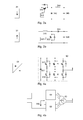
- Fig. 1 shows the basic principle of a first circuit arrangement according to the invention, as well as some of its components.
- Fig. 2 shows further components of a circuit arrangement according to the invention.
- Fig. 3 shows the basic principle of a further embodiments of the circuit arrangement according to the invention.
- Fig. 4 shows further components of a circuit arrangement according to the invention.
- Fig. 5 shows the simulation of the output current of a circuit arrangement according to the invention when using a method according to the invention.
- Fig. 1 shows schematically the basic principle of a first circuit arrangement according to the invention, as well as some of its components.
- an unregulated voltage source (12) here a photovoltaic system
- the known fluctuations in the DC output voltage as well as the output current due to the variation of solar radiation.
- MPP tracking For advantageous operation of such a photovoltaic system (12), it is necessary to regulate the output voltage and current in such a way that the output power is maximum. This is known as MPP tracking.
- MPP tracking MPP tracking.
- a voltage doubler circuit (20) adjoins the output of the photovoltaic system (12), which leads to an output current without short-term fluctuations.
- This voltage doubler circuit (20) shown in FIG Fig. 1b each having a branch of positive and negative polarity has an associated inductance (200, 202) in each branch.
- This inductance (200, 202) is formed here by the connecting lines between the photovoltaic system and the other components of the voltage doubling circuit. If the inductance (200, 202) of these leads should not be sufficient, it is additionally possible to provide coils with low inductance in comparison to the prior art.
- the voltage doubling circuit (20) here includes the connection line with the photovoltaic system (12). These connecting cables have a length dimension of the order of ten meters.
- a half-bridge circuit is provided between the positive and the negative branch.
- This half-bridge circuit in turn has a series connection of a first (210) and a second power transistor (212), possibly with antiparallel-connected freewheeling diodes.
- This half-bridge circuit is connected by means of a respective diode (220, 222) per branch to a series circuit (230, 232) of second capacitors (230, 232).
- a series circuit 230, 232
- the cathode is connected to the capacitor circuit.
- the cathode is connected to the half-bridge circuit and the anode to the capacitor circuit.
- both power transistors (210, 212) are switched on alternately for the same time interval in each case with a moderate switching frequency of preferably between 500 Hz and 2 kHz. There are also switching frequencies below 250Hz and up to 5kHz suitable but usually not necessary. Thus, there is always a current flow either through the first or through the second power transistor (210, 212) and thus the current load of the photovoltaic system (12) is kept constant. Constant means here there are no short-term fluctuations, especially in the order of magnitude of the drive frequency of the power transistor (210, 212).
- the voltage doubler circuit is followed by a voltage regulating circuit (30, 40), which can be designed differently depending on the conditions of use.
- the first variant has a combination of a down (34) and an up converter (32) whose order is basically arbitrary. Here, however, it is essential that the two converter circuits are not arranged directly adjacent, but that their connection line (300), according to Fig. 1c / d, the substantial distance between the photovoltaic system (12) and the inverter circuit (50) bridges.
- the voltage in the connection line (300) can be set below a defined threshold, illustratively below 600V or below 1000V. This can be the hassle for the Protection against contact dependent on national regulations against higher voltages substantially simplify.
- the second variant has as a voltage regulating circuit (40) to a subcircuit, which is identical to the voltage doubling circuit (20) is formed, but not how it is driven.
- the two switches are preferably for the same time intervals but with a suitable length and possibly overlap controlled to adjust the fluctuating input voltage to the desired constant output voltage.
- the MPP tracking of the photovoltaic system (12) is controlled by the voltage regulating circuit (30, 40), not by the voltage doubling circuit (20).
- the voltage doubler circuit (20) it is not necessary for the voltage doubler circuit (20) to have a control connection of its controller (250) to the voltage regulator circuit (30, 40) or the inverter circuit (50).
- the photovoltaic system (12), the voltage doubler circuit (20) and the respective voltage regulation circuit (30, 40) form a subcircuit arrangement, which is connected to an inverter circuit (50) to form a circuit arrangement according to the invention.
- Fig. 2 shows components of a circuit arrangement according to the invention, here the two converter circuits, which correspond to the prior art.
- the down converter (34) In its first branch, the one of positive polarity, has a power transistor (340). This is followed by a diode (342) connecting the first to the second branch and an inductor (344) in the first branch and a capacitor (346) connecting both branches. It may be sufficient in the above-mentioned application with a connection line following the down converter (34), said inductance (344) being determined by the inductance of the connection line (300, cf. Fig. 1d ) form, or provide a correspondingly small-sized coil.
- the boost converter (32), according to Fig. 2b Has in its first branch on an inductance (320), which also advantageously by a connecting line (300, see Fig. 1c ), possibly with an additional coil of low inductance, is formed. This is followed by a power transistor (322) connecting the first to the second branch and a diode (324) in the first branch and a capacitor (326) connecting both branches.
- Fig. 3 shows the basic principle of a further embodiments of the circuit arrangement according to the invention.
- Fig. 3a shown here is the arrangement of sub-circuits (10), according to the first variant, as to Fig. 1 described, with a voltage control circuit consisting of two converter circuits (32, 34) is constructed.
- the subcircuits in the region of the connections (300) of the two converter circuits (32, 34) are connected to one another and connected in parallel with one another.
- the outputs of the respective subcircuits are then connected to a suitable inverter circuit (50).
- Fig. 3b shows an arrangement according to the second above Fig. 1 mentioned variant with two identically designed but differently driven circuits for voltage doubling (20) and voltage regulation (40).
- the outputs of the subcircuits are connected to each other and to a suitable inverter circuit (50).
- Fig. 4 shows further components, here two embodiments of the inverter circuit (50), a circuit arrangement according to the invention.
- the inverter circuit is designed as a three-phase bridge circuit (60) according to the prior art, shown in FIG Fig. 4a ,
- two parallel three-phase bridge circuit (60) to switch parallel and offset from each other by half a switching period to clock.
- the midpoint of the two three-phase bridge circuits (60) can be at ground potential (612) or at the middle potential (212) of the voltage doubler circuit (20).
- Fig. 5 shows the simulation of the output current of a circuit arrangement according to the invention with an inverter circuit (50) according to Fig. 4b when using the method according to the invention mentioned therein in comparison to the output current of an inverter circuit according to FIG Fig. 4a ,
- the ripple can be significantly reduced within the respective sinusoids of the three phases of the output current.
Abstract
Description
Die Erfindung beschreibt eine Schaltungsanordnung, sowie ein Verfahren zu deren Ansteuerung, zur Erzeugung einer Wechselspannung aus einer Mehrzahl von ungeregelten Spannungsquellen mit zeitlich variabler Ausgangsgleichspannung. Als derartige ungeregelte Spannungsquellen sind Photovoltaikanlagen oder Teile dieser Anlagen bevorzugt. Unter einer Photovoltaikanlage soll hier ausschließlich die Anordnung und elektrische Verbindung einer Mehrzahl von Photovoltaikmodulen verstanden werden, Teilanlagen sind hier ebenfalls subsumiert. Derartige Photovoltaikmodule sind zu Photovoltaikanlagen zusammengeschlossen und weisen eine bauartbedingte und von der Sonneneinstrahlung abhängige und somit zeitlich langsam variable Ausgangsgleichspannung auf. Diese Änderungen der Ausgangsgleichspannung weisen Zeitkonstanten im Minutenbereich oder in längeren Zeiteinheiten auf.The invention relates to a circuit arrangement, as well as a method for the control thereof, for generating an AC voltage from a plurality of unregulated voltage sources with time-variable DC output voltage. As such unregulated power sources, photovoltaic systems or parts of these systems are preferred. A photovoltaic system is to be understood here exclusively as the arrangement and electrical connection of a plurality of photovoltaic modules, subsystems are also subsumed here. Such photovoltaic modules are combined to photovoltaic systems and have a design-dependent and dependent on the sunlight and thus temporally slowly variable output DC voltage. These changes in the DC output voltage have time constants in the minute range or in longer time units.
Zu Einspeisung des Ausgangsstroms einer derartigen Photovoltaikanlagen in das öffentliche oder ein lokales Stromnetz muss die Ausgangsgleichspannung, mittels einer Wechselrichterschaltung, in eine Wechselspannung konstanter Frequenz und Spannung umgewandelt werden.To feed the output current of such a photovoltaic systems in the public or a local power grid, the DC output voltage must be converted by means of an inverter circuit in an AC voltage of constant frequency and voltage.
Eine beispielhafte Schaltungsanordnung zur Erzeugung einer derartigen Wechselspannung ist in der
Für derartige Schaltungsanordnungen gibt es eine Vielzahl vom Anwendungsfall abhängiger und sich teilweise widerstrebender Anforderungen. Beispielhafte sollen die einzelnen Photovoltaikmodule möglichst linear belastet werden, d.h. deren Ausgangsstrom soll zeitlich möglichst konstant sein innerhalb von Zeitintervallen, wie sie für Leistungshalbleiterschaltungen typisch sind, also im Zeitbereich kleiner einer Sekunde, bzw. in einem Frequenzbereich oberhalb von 1Hz. Ebenso soll die Eingangsspannung an der Wechselrichterschaltung möglichst konstant sein, wie auch die Übertragung von der Photovoltaikanlage zur Wechselrichterschaltung mit möglichst hoher Spannung erfolgen soll, um Leitungsverluste klein zu halten.For such circuits, there are a variety of application dependent and partially conflicting requirements. By way of example, the individual photovoltaic modules should be loaded as linearly as possible, i. Their output current should be as constant as possible in time within time intervals, as they are typical for power semiconductor circuits, ie in the time domain less than one second, or in a frequency range above 1Hz. Likewise, the input voltage to the inverter circuit should be as constant as possible, as well as the transmission from the photovoltaic system to the inverter circuit with the highest possible voltage should be done to keep line losses small.
Schließlich soll die gesamte Schaltungsanordnung mit einem hohen Wirkungsgrad arbeiten, hierbei die Anzahl der notwendigen Komponenten klein und deren Dimensionierung, speziell diejenige von Spulen und Kondensatoren ebenfalls möglichst klein sein. Gleichzeitig sollte die Photovoltaikanlage, bzw. deren Photovoltaikmodule, derart betrieben werden, dass sie im Punkt der höchsten Leistungsabgabe (MPP - maximum power point) arbeitet. Hierzu ist eine geeignete Regelung, das sog. MPP-Tracking erforderlich.Finally, the entire circuit arrangement should work with a high degree of efficiency, in this case the number of components required being small and their dimensioning, especially that of coils and capacitors, also be as small as possible. At the same time, the photovoltaic system or its photovoltaic modules should be operated in such a way that it operates at the point of the highest power output (MPP). For this purpose, a suitable regulation, the so-called. MPP tracking is required.
Der Erfindung liegt die Aufgabe zugrunde eine Schaltungsanordnung und ein zugehöriges Verfahren vorzustellen zur Erzeugung einer Wechselspannung aus einer Mehrzahl von Spannungsquellen mit jeweils zeitlich variabler Ausgangsgleichspannung, wobei die Strombelastung diese Spannungsquellen gleichmäßig und die Übertragung zur Wechselrichterschaltung mit möglichst geringen Verlusten behaftet ist.The invention has for its object to provide a circuit arrangement and an associated method for generating an AC voltage from a plurality of voltage sources, each with time-varying DC output voltage, the current load is uniformly these voltage sources and the transfer to the inverter circuit with minimal losses.
Die Aufgabe wird erfindungsgemäß gelöst, durch eine Schaltungsanordnung mit den Merkmalen des Anspruchs 1, sowie durch ein Verfahren gemäß Anspruch 8. Bevorzugte Ausführungsformen sind in den jeweiligen abhängigen Ansprüchen beschrieben.The object is achieved by a circuit arrangement with the features of claim 1, and by a method according to claim 8. Preferred embodiments are described in the respective dependent claims.
Die erfindungsgemäße Schaltungsanordnung weist eine oder eine Mehrzahl parallel geschalteter Teilschaltungsanordnungen zur Speisung mindestens einer Wechselrichterschaltung, die mit mindesten einem zugeordneten Transformator verbindbar ist. Hierbei besteht jede Teilschaltungsanordnung aus einer ungeregelten Spannungsquelle mit zeitlich variierender Ausgangsgleichspannung, einer Spannungsverdoppelungsschaltung und einer Spannungsregelschaltung mit zugeordneter Regelungseinrichtung.The circuit arrangement according to the invention comprises one or a plurality of parallel-connected subcircuit arrangements for feeding at least one inverter circuit, which can be connected to at least one associated transformer. In this case, each subcircuit arrangement consists of an unregulated voltage source with a time-varying DC output voltage, a voltage doubler circuit and a voltage regulator circuit with associated control device.
Bei dem erfindungsgemäßen Verfahren zur Ansteuerung einer derartigen Schaltungsanordnung wird mittels der Spannungsverdoppelungsschaltung die Eingangsspannung verdoppelt, indem die beiden Leistungstransistoren der Halbbrückenschaltung zeitlich versetzt und jeweils mit gleicher Periodendauer von jeweils der Hälfte der Schaltperiode eingeschaltet werden. Hierdurch wird die ungeregelte Spannungsquelle konstant belastet, das heißt ihr Ausgangsstrom weist keine Schwankungen im Kurzzeitbereich, also im Bereich von einer Sekunde oder schneller auf, wie dies speziell für Photovoltaikanlagen bzw. Photovoltaikmodule bevorzugt ist.In the method according to the invention for driving such a circuit arrangement, the input voltage is doubled by means of the voltage doubling circuit by the two power transistors of the half-bridge circuit being offset in time and each with the same period of half of the switching period. As a result, the unregulated voltage source is charged constantly, that is, their output current has no fluctuations in the short-term range, ie in the range of one second or faster, as is particularly preferred for photovoltaic or photovoltaic modules.
Es ist bevorzugt, wenn die Spannungsverdoppelungsschaltung je einen Zweig positiver und negativer Polarität aufweist, wobei an deren Eingängen jeweils eine erste und zweite Induktivität, gebildet aus einer ersten und zweiten Spule oder auch nur aus der Induktivität der jeweiligen Zuleitung von der Spannungsquelle vorgesehen ist. An diese erste und zweite Induktivität schießt eine Halbbrückenschaltung zweier Leistungstransistoren zwischen dem positiven und dem negativen Zeig an. Anschließend ist in beiden Zweigen jeweils eine Diode und hieran anschließend ein Reihenschaltung zweier erster Kondensator vorgesehen, die beide Zweige verbindet.It is preferred if the voltage doubling circuit each has a branch of positive and negative polarity, wherein at their inputs in each case a first and second inductance, formed from a first and second coil or only from the inductance of the respective supply line from the voltage source is provided. At this first and second inductance shoots a half-bridge circuit of two power transistors between the positive and the negative pointer. Subsequently, in each case a diode is provided in both branches, and thereafter a series connection of two first capacitors, which connects the two branches.
Für die Ausgestaltung der Spannungsregelschaltung sind grundsätzlich zwei Varianten besonders bevorzugt. Die erste Variante weist zwei getrennte Teilschaltungen einen Aufwärts- und einen Abwärtswandler auf. Für deren Anordnung sind ebenfalls zwei Varianten vorteilhaft. In einer ersten Variante sind die jeweiligen Aufwärtswandler direkt im Anschluss an die zugeordneten Spannungsverdoppelungsschaltungen vorgesehen um deren Ausgangsspannungen auf gleiches Potential anzuheben. Der jeweilige Abwärtswandler ist dann bei der Wechselrichterschaltung vorgesehen um dort die Übertragungsspannung auf einen geeigneten Wert der Zwischenkreisspannung abzusenken. Diese Variante hat den Vorteil eine besonders hohe Spannung zur Leistungsübertragung zwischen Photovoltaikanlage und Wechselrichterschaltung zur Verfügung zu stellen und damit die Leitungsverluste bestmöglich gering zu halten. Somit kann auch die Dimensionierung der Übertragungskabel und die damit verbundene Kosten wegen des geringeren Wertes des Übertragungsstroms reduziert werden.In principle, two variants are particularly preferred for the design of the voltage regulation circuit. The first variant has two separate sub-circuits, an up-converter and a down-converter. For their arrangement, two variants are also advantageous. In a first variant, the respective boost converters are provided immediately after the associated voltage doubler circuits in order to raise their output voltages to the same potential. The respective down converter is then provided in the inverter circuit to lower the transmission voltage there to a suitable value of the intermediate circuit voltage. This variant has the advantage of providing a particularly high voltage for power transmission between the photovoltaic system and the inverter circuit and thus to keep the line losses as low as possible. Consequently Also, the dimensioning of the transmission cables and the associated costs can be reduced because of the lower value of the transmission current.
Die zweite Variante mit zwei getrennten Teilschaltungen weist den jeweiligen Abwärtswandler im direkten Anschluss an die zugeordnete Spannungsverdoppelungsschaltung auf, während der Aufwärtswandler bei der Wechselrichterschaltung angeordnet ist. Somit erfolgt die Übertragung bei geringerer Spannung verglichen mit der ersten Variante. Dies kann allerdings vorteilhaft sein um die Gesamtanlage an Sicherheitsrichtlinien anzupassen und beispielhafte besondere Schutzvorschriften für höhere Spannungen nicht realisieren zu müssen. Insgesamt bietet die Spannungsregelschaltung mit zwei getrennten Wandlerschaltungen eine hohe Flexibilität zu Anpassung der Teilschaltungsanordnung an die anwendungsspezifischen Gegebenheiten.The second variant with two separate subcircuits has the respective buck converter in direct connection with the associated voltage doubler circuit, while the upconverter is located in the inverter circuit. Thus, the transmission is carried out at a lower voltage compared to the first variant. However, this can be advantageous in order to adapt the overall system to safety guidelines and not have to implement exemplary special protection regulations for higher voltages. Overall, the voltage regulation circuit with two separate converter circuits offers a high degree of flexibility for adapting the subcircuit arrangement to the application-specific circumstances.
Die zweite Variante der Spannungsregelschaltung ist grundsätzlich identisch der Spannungsverdoppelungsschaltung aufgebaut und kann somit vorteilhafterweise auch mit identischen Leistungshalbleitermodulen erstellt werden. Diese Spannungsregelschaltung wird allerdings entsprechend ihrer Aufgabe unterschiedlich zur Spannungsverdoppelungsschaltung angesteuert und dient der Anpassung der Ausgangsgleichspannung der verschiedenen zueinander parallel zu schaltenden Teilschaltungsanordnungen.The second variant of the voltage regulation circuit is basically constructed identically to the voltage doubling circuit and can thus be advantageously produced with identical power semiconductor modules. However, this voltage regulation circuit is controlled differently according to its task to the voltage doubling circuit and serves to adapt the output DC voltage of the different circuit elements to be switched in parallel to each other.
Das bei Photovoltaikanlagen notwendige regeln der Strom- / Spannungskennlinie, das MPP- Tracking, erfolgt ebenfalls durch die Regelungseinrichtung der Spannungsregelschaltung zusätzlich zur beschriebenen Anpassung der Ausgangsspannung der Spannungsverdoppelungsschaltung an die Zwischenkreisspannung der Wechselrichterschaltung.The necessary in photovoltaic systems regulating the current / voltage characteristic, the MPP tracking is also carried out by the control device of the voltage control circuit in addition to the described adaptation of the output voltage of the voltage doubling circuit to the DC link voltage of the inverter circuit.
Als Wechselrichterschaltung sind grundsätzlich verschieden Drei- Phasen-Wechselrichter vorsehbar. Besonders vorteilhaft ist es zwei Drei- Phasen- Wechselrichter parallel anzuordnen und um eine halbe Schaltperiode versetzten anzusteuern. Hierdurch ergibt sich ein dem gewünschten sinusförmigen Ausgang ausreichend angenäherte Spannung.As inverter circuit fundamentally different three-phase inverters are providable. It is particularly advantageous to arrange two three-phase inverters in parallel and offset by half a switching period to control. This results in a desired sinusoidal output sufficiently approximated voltage.
Die erfinderische Lösung wird an Hand der Ausführungsbeispiele der
Daher schließt sich erfindungsgemäß an den Ausgang der Photovoltaikanlage (12) eine Spannungsverdoppelungsschaltung (20) an, die zu einem Ausgangsstrom ohne kurzzeitige Schwankungen führt. Diese Spannungsverdoppelungsschaltung (20), dargestellt in
Anschließend an die Induktivitäten (200, 202) ist eine Halbbrückenschaltung zwischen dem positiven und dem negativen Zweig vorgesehen. Diese Halbbrückenschaltung weist ihrerseits eine Reihenschaltung eines ersten (210) und eines zweiten Leistungstransistors (212), ggf. mit antiparallel geschalteten Freilaufdioden, auf.Subsequent to the inductors (200, 202), a half-bridge circuit is provided between the positive and the negative branch. This half-bridge circuit in turn has a series connection of a first (210) and a second power transistor (212), possibly with antiparallel-connected freewheeling diodes.
Diese Halbbrückenschaltung ist mittels je einer Diode (220, 222) pro Zweig mit einer Reihenschaltung (230, 232) zweiter Kondensatoren (230, 232) verbunden. Hierbei ist im ersten dem Zweig positiver Polarität die Anode der Diode mit der Halbbrückenschaltung und die Kathode mit der Kondensatorschaltung verbunden. Im zweiten, dem Zweig negativer Polarität, ist die Kathode mit der Halbbrückenschaltung und die Anode mit der Kondensatorschaltung verbunden.This half-bridge circuit is connected by means of a respective diode (220, 222) per branch to a series circuit (230, 232) of second capacitors (230, 232). Here, in the first branch of the positive polarity, the anode of the diode is connected to the half-bridge circuit and the cathode is connected to the capacitor circuit. In the second, the branch of negative polarity, the cathode is connected to the half-bridge circuit and the anode to the capacitor circuit.
Es ist weiterhin bevorzugt, wenn die jeweiligen Mittelanzapfungen der Halbbrückenschaltung und der Kondensatorschaltung miteinander verbunden sind. Zur Funktion als Spannungsverdoppelungsschaltung (20) werden beide Leistungstransistoren (210, 212) alternierend für jeweils das gleiche Zeitintervall mit einer moderaten Schaltfrequenz von vorzugsweise zwischen 500Hz und 2kHz angeschaltet. Es sind auch Schaltfrequenzen unterhalb von 250Hz und bis zu 5kHz geeignet aber in der Regel nicht notwendig. Es ist somit jederzeit ein Stromfluss entweder durch den ersten oder durch den zweiten Leistungstransistor (210, 212) gegeben und somit wird die Strombelastung des Photovoltaikanlage (12) konstant gehalten. Konstant meint hier es treten keine kurzzeitigen Schwankungen speziell in der Größenordnung der Ansteuerfrequenz der Leistungstransistor (210, 212) auf.It is furthermore preferred if the respective center taps of the half-bridge circuit and of the capacitor circuit are connected to one another. For function as a voltage doubling circuit (20), both power transistors (210, 212) are switched on alternately for the same time interval in each case with a moderate switching frequency of preferably between 500 Hz and 2 kHz. There are also switching frequencies below 250Hz and up to 5kHz suitable but usually not necessary. Thus, there is always a current flow either through the first or through the second power transistor (210, 212) and thus the current load of the photovoltaic system (12) is kept constant. Constant means here there are no short-term fluctuations, especially in the order of magnitude of the drive frequency of the power transistor (210, 212).
An die Spannungsverdoppelungsschaltung schließt sich eine Spannungsregelschaltung an (30, 40), die abhängig von den Einsatzbedingungen unterschiedlich ausgestaltet sein kann. Die erste Variante weist eine Kombination aus einem Abwärts- (34) und einem Aufwärtswandler (32) auf, deren Reihenfolge grundsätzlich beliebig ist. Hier ist allerdings wesentlich, das die beiden Wandlerschaltungen nicht direkt benachbart angeordnet sind, sondern, dass ihre Verbindungsleitung (300), gemäß
Somit kann durch Anordnung eines Abwärtswandlers (34) im Anschluss an die Spannungsverdoppelungsschaltung (20) die Spannung in der Verbindungsleitung (300) auf einen Wert unterhalb einer definierten Schwelle, beispielhafte unterhalb von 600V oder unterhalb von 1000V eingestellt werden. Dies kann den Aufwand für den Berührungsschutz abhängigen von nationalen Vorschriften gegenüber höheren Spannungen wesentlich vereinfachen.Thus, by placing a down converter (34) following the voltage doubler circuit (20), the voltage in the connection line (300) can be set below a defined threshold, illustratively below 600V or below 1000V. This can be the hassle for the Protection against contact dependent on national regulations against higher voltages substantially simplify.
Eine analoge Ausgestaltung mit Vertauschung der beiden Wandlerschaltungen (32, 34) ermöglicht demgegenüber eine möglichst hohe Spannungen in der Verbindungsleitung (300), die somit einen entsprechend kleineren Wert des Stromes nach sich zieht und damit bezüglich elektrischen Verlusten, der Dimensionierung und auch der Kosten dieser Verbindungsleitung (300) vorteilhaft ist.By contrast, an analog configuration with interchanging of the two converter circuits (32, 34) allows the highest possible voltages in the connecting line (300), which thus entails a correspondingly smaller value of the current and thus with respect to electrical losses, dimensioning and also the costs thereof Connecting line (300) is advantageous.
Die zweite Variante weist als Spannungsregelschaltung (40) eine Teilschaltung auf, die identisch der Spannungsverdoppelungsschaltung (20) ausgebildet ist, allerdings nicht wie diese angesteuert wird. Zur Spannungsregelung werden die beiden Schalter vorzugsweise für jeweils gleiche Zeitintervalle aber mit geeigneter Länge und ggf. Überlappung angesteuert um die schwankende Eingangsspannung an die gewünschte konstante Ausgangsspannung anzupassen.The second variant has as a voltage regulating circuit (40) to a subcircuit, which is identical to the voltage doubling circuit (20) is formed, but not how it is driven. For voltage regulation, the two switches are preferably for the same time intervals but with a suitable length and possibly overlap controlled to adjust the fluctuating input voltage to the desired constant output voltage.
In beiden Varianten wird das MPP- Tracking der Photovoltaikanlage (12) durch die Spannungsregelschaltung (30, 40), nicht durch die Spannungsverdoppelungsschaltung (20), gesteuert. Somit ist es nicht notwendig, dass die Spannungsverdoppelungsschaltung (20) eine Steuerverbindung ihrer Regeleinrichtung (250) mit der Spannungsregelschaltung (30, 40) oder der Wechselrichterschaltung (50) aufweist.In both variants, the MPP tracking of the photovoltaic system (12) is controlled by the voltage regulating circuit (30, 40), not by the voltage doubling circuit (20). Thus, it is not necessary for the voltage doubler circuit (20) to have a control connection of its controller (250) to the voltage regulator circuit (30, 40) or the inverter circuit (50).
Die Photovoltaikanlage (12), die Spannungsverdoppelungsschaltung (20) und die jeweilige Spannungsregelschaltung (30, 40) bilden eine Teilschaltungsanordnung, die mit einer Wechselrichterschaltung (50) zu einer erfindungsgemäßen Schaltungsanordnung verbunden ist.The photovoltaic system (12), the voltage doubler circuit (20) and the respective voltage regulation circuit (30, 40) form a subcircuit arrangement, which is connected to an inverter circuit (50) to form a circuit arrangement according to the invention.
Der Aufwärtswandler (32), gemäß
Es ist allerdings, dargestellt in
Die gesamte Schaltungsanordnung vereint somit die Vorteile:
- ●konstante Belastung der Spannungsquelle.
- ●Flexible Wahl der Übertragungsspannung zur Wechselrichterschaltung.
- ●lein dimensionierte Spulen in der Spannungsverdoppelungsschaltung und in den Spannungsregelschaltungen.
- ●usgangsstrom geringer Welligkeit.
- ● constant load of the voltage source.
- ● Flexible selection of the transfer voltage to the inverter circuit.
- ● dimensioned coils in the voltage doubling circuit and in the voltage regulation circuits.
- ● Output current low ripple.
Claims (10)
die Spannungsverdoppelungsschaltung (20) je einen Zweig positiver und negativer Polarität aufweist, wobei an deren Eingängen jeweils eine erste (200) und zweite Induktivität (202), gebildet aus einer ersten und zweiten Spule oder aus der Induktivität der jeweiligen Zuleitung von der Spannungsquelle (12) vorgesehen ist, sich hieran eine Halbbrückenschaltung zweier Leistungstransistoren (210, 212) zwischen dem positiven und dem negativen Zeig anschließt, und in beiden Zweigen weiterhin jeweils eine Diode (220, 222) und hieran anschließend eine Reihenschaltung zweier erster Kondensator (230, 232), die beide Zweige verbindet, vorgesehen ist.Circuit arrangement according to claim 1, wherein
the voltage doubler circuit (20) has a respective branch of positive and negative polarity, wherein at their inputs in each case a first (200) and second inductance (202), formed from a first and second coil or from the inductance of the respective supply line from the voltage source (12 ) is provided, this is followed by a half-bridge circuit of two power transistors (210, 212) between the positive and the negative pointer, and in both branches each further comprise a diode (220, 222) and then a series connection of two first capacitor (230, 232) , which connects both branches, is provided.
die Mittelanzapfungen der Halbbrückenschaltung 210, 212) und der Reihenschaltung der Kondensatoren (230, 232) miteinander verbunden sind.Circuit arrangement according to claim 2, wherein
the center taps of the half-bridge circuit 210, 212) and the series circuit of the capacitors (230, 232) are interconnected.
die Spannungsregelschaltung aus einem Abwärtswandler (34) mit einem Leistungstransistor (340) im positiven Zweig, einer den positiven und negativen Zweig verbindenden Diode (342) und einer dritten Induktivität (344), vorzugsweise einer dritten Spule, und einem vor- oder nachgeschalteten Aufwärtswandler (32), mit einer vierten Induktivität (320), vorzugsweise einer vierten Spule, einem den positiven und negativen Zweig verbindenden Leistungstransistor (322) und einer Diode (324) im positiven Zweig besteht.Circuit arrangement according to claim 1, wherein
the voltage regulation circuit comprising a down-converter (34) having a power transistor (340) in the positive branch, a diode (342) connecting the positive and negative branches, and a third inductor (344), preferably a third coil, and a forward or a step-up ( 32), a fourth inductor (320), preferably a fourth coil, a positive and negative branch connecting power transistor (322) and a diode (324) in the positive branch.
der Abwärtswandler (34) direkt benachbart zur Spannungsverdoppelungsschaltung (20) und diese direkt benachbart zur Spannungsquelle (12) angeordnet ist und wobei der Aufwärtswandler (32) direkt benachbart zur Wechselrichterschaltung (50) angeordnet ist.Circuit arrangement according to claim 4, wherein
the down-converter (34) is disposed directly adjacent to the voltage doubler circuit (20) and directly adjacent to the voltage source (12), and wherein the up-converter (32) is disposed directly adjacent to the inverter circuit (50).
der Aufwärtswandler (32) direkt benachbart zur Spannungsverdoppelungsschaltung (20) und diese direkt benachbart zur Spannungsquelle (12) angeordnet ist und wobei der Abwärtswandler (34) direkt benachbart zur Wechselrichterschaltung (50) angeordnet ist.Circuit arrangement according to claim 4, wherein
the boost converter (32) is located immediately adjacent to the voltage doubler circuit (20) and directly adjacent to the voltage source (12), and wherein the down converter (34) is disposed directly adjacent to the inverter circuit (50).
die Spannungsregelschaltung (40) analog zur Spannungsverdoppelungsschaltung (20) ausgebildet ist.Circuit arrangement according to claim 1, wherein
the voltage regulation circuit (40) is designed analogously to the voltage doubler circuit (20).
die Spannungsverdoppelungsschaltung (20) die Spannung der ungeregelten Spannungsquelle (12) verdoppelt, indem die beiden Leistungstransistoren (210, 212) der Halbbrückenschaltung zeitlich versetzt und jeweils mit gleicher Periodendauer von jeweils der Hälfte der Schaltperiode eingeschaltet werden.The method of claim 8, wherein
the voltage doubler circuit (20) doubles the voltage of the unregulated voltage source (12) by the two power transistors (210, 212) of the half-bridge circuit being switched off in time and each with the same period duration of each half of the switching period.
die beiden Leistungstransistoren (210, 212) der Spannungsverdoppelungsschaltung (20) mit einer Frequenz zwischen 250Hz und 5kHz, vorzugsweise zwischen 500Hz und 2kHz angesteuert werden.The method of claim 9, wherein
the two power transistors (210, 212) of the voltage doubler circuit (20) are driven at a frequency between 250Hz and 5kHz, preferably between 500Hz and 2kHz.
Applications Claiming Priority (1)
| Application Number | Priority Date | Filing Date | Title |
|---|---|---|---|
| DE102010013138A DE102010013138A1 (en) | 2010-03-27 | 2010-03-27 | Circuit arrangement and method for generating an AC voltage from a plurality of voltage sources with time-varying DC output voltage |
Publications (3)
| Publication Number | Publication Date |
|---|---|
| EP2369733A2 true EP2369733A2 (en) | 2011-09-28 |
| EP2369733A3 EP2369733A3 (en) | 2016-04-27 |
| EP2369733B1 EP2369733B1 (en) | 2016-11-23 |
Family
ID=44276222
Family Applications (1)
| Application Number | Title | Priority Date | Filing Date |
|---|---|---|---|
| EP11151095.4A Not-in-force EP2369733B1 (en) | 2010-03-27 | 2011-01-17 | Circuit assembly and method for generating alternating current from a number of power supply units with output DC voltage which varies over time |
Country Status (6)
| Country | Link |
|---|---|
| US (1) | US8711590B2 (en) |
| EP (1) | EP2369733B1 (en) |
| KR (1) | KR20110109884A (en) |
| CN (1) | CN102201753B (en) |
| BR (1) | BRPI1101071A2 (en) |
| DE (1) | DE102010013138A1 (en) |
Cited By (2)
| Publication number | Priority date | Publication date | Assignee | Title |
|---|---|---|---|---|
| EP2713499A1 (en) * | 2012-09-28 | 2014-04-02 | Siemens Aktiengesellschaft | Energy feed device with symmetrical connection of a direct current source to a grounded star point of a three-phase current network |
| EP2713494A1 (en) * | 2012-09-28 | 2014-04-02 | Siemens Aktiengesellschaft | Energy feed device for feeding electrical energy generated from kinetic energy into an alternating current distributor network |
Families Citing this family (4)
| Publication number | Priority date | Publication date | Assignee | Title |
|---|---|---|---|---|
| DE102007054647A1 (en) * | 2007-11-15 | 2009-06-18 | Siemens Ag | Solar inverter with several parallel single inverters and with a higher-level electronic control unit |
| US9001518B2 (en) * | 2011-04-26 | 2015-04-07 | International Rectifier Corporation | Power module with press-fit clamps |
| CN105634399A (en) * | 2014-10-28 | 2016-06-01 | 江苏绿扬电子仪器集团有限公司 | Inverter preceding-stage direct-current converter |
| CN105915047A (en) * | 2016-05-06 | 2016-08-31 | 上海交通大学 | Novel direct current boosted circuit |
Citations (1)
| Publication number | Priority date | Publication date | Assignee | Title |
|---|---|---|---|---|
| DE102008034955A1 (en) | 2008-07-26 | 2010-02-04 | Semikron Elektronik Gmbh & Co. Kg | Converter arrangement for solar power systems and Ansteuerverfahren this |
Family Cites Families (7)
| Publication number | Priority date | Publication date | Assignee | Title |
|---|---|---|---|---|
| US4135235A (en) * | 1977-10-31 | 1979-01-16 | Exxon Research & Engineering Co. | Synthesizer circuit for generating three-tier waveforms |
| EP1532727A2 (en) * | 2002-07-15 | 2005-05-25 | Koninklijke Philips Electronics N.V. | Inverter |
| US7319313B2 (en) * | 2005-08-10 | 2008-01-15 | Xantrex Technology, Inc. | Photovoltaic DC-to-AC power converter and control method |
| US7692411B2 (en) * | 2006-01-05 | 2010-04-06 | Tpl, Inc. | System for energy harvesting and/or generation, storage, and delivery |
| TWI346441B (en) * | 2006-11-10 | 2011-08-01 | Delta Electronics Inc | Three-level ac generating circuit and control method thereof |
| US7900361B2 (en) * | 2006-12-06 | 2011-03-08 | Solaredge, Ltd. | Current bypass for distributed power harvesting systems using DC power sources |
| EP3324505B1 (en) * | 2007-10-15 | 2023-06-07 | Ampt, Llc | Systems for highly efficient solar power |
-
2010
- 2010-03-27 DE DE102010013138A patent/DE102010013138A1/en not_active Withdrawn
-
2011
- 2011-01-17 EP EP11151095.4A patent/EP2369733B1/en not_active Not-in-force
- 2011-03-22 KR KR1020110025197A patent/KR20110109884A/en not_active Application Discontinuation
- 2011-03-25 CN CN201110079999.XA patent/CN102201753B/en not_active Expired - Fee Related
- 2011-03-28 BR BRPI1101071-1A patent/BRPI1101071A2/en not_active Application Discontinuation
- 2011-03-28 US US13/073,581 patent/US8711590B2/en not_active Expired - Fee Related
Patent Citations (1)
| Publication number | Priority date | Publication date | Assignee | Title |
|---|---|---|---|---|
| DE102008034955A1 (en) | 2008-07-26 | 2010-02-04 | Semikron Elektronik Gmbh & Co. Kg | Converter arrangement for solar power systems and Ansteuerverfahren this |
Cited By (2)
| Publication number | Priority date | Publication date | Assignee | Title |
|---|---|---|---|---|
| EP2713499A1 (en) * | 2012-09-28 | 2014-04-02 | Siemens Aktiengesellschaft | Energy feed device with symmetrical connection of a direct current source to a grounded star point of a three-phase current network |
| EP2713494A1 (en) * | 2012-09-28 | 2014-04-02 | Siemens Aktiengesellschaft | Energy feed device for feeding electrical energy generated from kinetic energy into an alternating current distributor network |
Also Published As
| Publication number | Publication date |
|---|---|
| EP2369733B1 (en) | 2016-11-23 |
| BRPI1101071A2 (en) | 2012-12-04 |
| CN102201753A (en) | 2011-09-28 |
| CN102201753B (en) | 2014-12-31 |
| US8711590B2 (en) | 2014-04-29 |
| EP2369733A3 (en) | 2016-04-27 |
| US20110235377A1 (en) | 2011-09-29 |
| KR20110109884A (en) | 2011-10-06 |
| DE102010013138A1 (en) | 2011-09-29 |
Similar Documents
| Publication | Publication Date | Title |
|---|---|---|
| DE112005000294B4 (en) | motor drive device | |
| EP2730019B1 (en) | Operating method for an inverter and network fault-tolerant inverter | |
| EP2030299A1 (en) | Inverter for feeding electrical energy into a power supply system | |
| EP2369733B1 (en) | Circuit assembly and method for generating alternating current from a number of power supply units with output DC voltage which varies over time | |
| EP2517344B1 (en) | Bidirectional dc converter with buffer capacitor and controllable voltage at the capacitor | |
| DE112016004961T5 (en) | Multiphase converter | |
| EP2395639A2 (en) | Circuit assembly and method for generating alternating current from at least one power supply units with output DC voltage which varies over time | |
| DE112009004627T5 (en) | Power conversion device | |
| EP2586646B1 (en) | Electrical power supply assembly for drive units, for operating a rail vehicle on electrical supply networks | |
| EP2911284B1 (en) | Switch assemblies and method for picking up electric power from multiple module strands | |
| DE102012216691A1 (en) | Converter circuit and method for controlling the converter circuit | |
| DE102008034955A1 (en) | Converter arrangement for solar power systems and Ansteuerverfahren this | |
| DE112017005404T5 (en) | DC-DC converter | |
| DE102017212462A1 (en) | Galvanically coupled electrical converter | |
| DE102013212426A1 (en) | Inverter arrangement with parallel-connected multi-stage converters and methods for their control | |
| DE102011116593B4 (en) | Inverter with asymmetrical chokes and a control unit for asymmetric operation of the chokes | |
| DE102013007056A1 (en) | DC converter | |
| WO2013135578A1 (en) | Circuit arrangement and method for converting and adapting a dc voltage, photovoltaic installation | |
| DE102014101571B4 (en) | INVERTER AND PROCESS FOR OPERATING AN INVERTER | |
| EP2856625B1 (en) | Voltage supply for an inverter | |
| EP3043461B1 (en) | Supply circuit for supplying a welding device | |
| EP3363091B1 (en) | Device and method for controlling a load flow in an alternating-voltage network | |
| DE102014005124A1 (en) | Circuit arrangement and method for exchanging electrical energy | |
| EP2771958B1 (en) | Tracking method and tracking device for a voltage transformer for a photovoltaic system | |
| EP2372889A2 (en) | Circuit assembly and method for generating alternating current from a number of unregulated power supply units with output DC voltage which varies over time |
Legal Events
| Date | Code | Title | Description |
|---|---|---|---|
| PUAI | Public reference made under article 153(3) epc to a published international application that has entered the european phase |
Free format text: ORIGINAL CODE: 0009012 |
|
| AK | Designated contracting states |
Kind code of ref document: A2 Designated state(s): AL AT BE BG CH CY CZ DE DK EE ES FI FR GB GR HR HU IE IS IT LI LT LU LV MC MK MT NL NO PL PT RO RS SE SI SK SM TR |
|
| AX | Request for extension of the european patent |
Extension state: BA ME |
|
| 17P | Request for examination filed |
Effective date: 20151007 |
|
| PUAL | Search report despatched |
Free format text: ORIGINAL CODE: 0009013 |
|
| AK | Designated contracting states |
Kind code of ref document: A3 Designated state(s): AL AT BE BG CH CY CZ DE DK EE ES FI FR GB GR HR HU IE IS IT LI LT LU LV MC MK MT NL NO PL PT RO RS SE SI SK SM TR |
|
| AX | Request for extension of the european patent |
Extension state: BA ME |
|
| RIC1 | Information provided on ipc code assigned before grant |
Ipc: H02M 7/5387 20070101ALI20160322BHEP Ipc: H02M 7/537 20060101ALI20160322BHEP Ipc: H02M 1/00 20060101ALI20160322BHEP Ipc: H02M 7/48 20070101AFI20160322BHEP |
|
| GRAP | Despatch of communication of intention to grant a patent |
Free format text: ORIGINAL CODE: EPIDOSNIGR1 |
|
| INTG | Intention to grant announced |
Effective date: 20160914 |
|
| GRAS | Grant fee paid |
Free format text: ORIGINAL CODE: EPIDOSNIGR3 |
|
| GRAA | (expected) grant |
Free format text: ORIGINAL CODE: 0009210 |
|
| AK | Designated contracting states |
Kind code of ref document: B1 Designated state(s): AL AT BE BG CH CY CZ DE DK EE ES FI FR GB GR HR HU IE IS IT LI LT LU LV MC MK MT NL NO PL PT RO RS SE SI SK SM TR |
|
| REG | Reference to a national code |
Ref country code: GB Ref legal event code: FG4D Free format text: NOT ENGLISH |
|
| REG | Reference to a national code |
Ref country code: CH Ref legal event code: EP |
|
| REG | Reference to a national code |
Ref country code: IE Ref legal event code: FG4D Free format text: LANGUAGE OF EP DOCUMENT: GERMAN |
|
| REG | Reference to a national code |
Ref country code: AT Ref legal event code: REF Ref document number: 848702 Country of ref document: AT Kind code of ref document: T Effective date: 20161215 |
|
| REG | Reference to a national code |
Ref country code: DE Ref legal event code: R096 Ref document number: 502011011179 Country of ref document: DE |
|
| PG25 | Lapsed in a contracting state [announced via postgrant information from national office to epo] |
Ref country code: LV Free format text: LAPSE BECAUSE OF FAILURE TO SUBMIT A TRANSLATION OF THE DESCRIPTION OR TO PAY THE FEE WITHIN THE PRESCRIBED TIME-LIMIT Effective date: 20161123 |
|
| REG | Reference to a national code |
Ref country code: LT Ref legal event code: MG4D |
|
| REG | Reference to a national code |
Ref country code: NL Ref legal event code: MP Effective date: 20161123 |
|
| PG25 | Lapsed in a contracting state [announced via postgrant information from national office to epo] |
Ref country code: LT Free format text: LAPSE BECAUSE OF FAILURE TO SUBMIT A TRANSLATION OF THE DESCRIPTION OR TO PAY THE FEE WITHIN THE PRESCRIBED TIME-LIMIT Effective date: 20161123 Ref country code: NO Free format text: LAPSE BECAUSE OF FAILURE TO SUBMIT A TRANSLATION OF THE DESCRIPTION OR TO PAY THE FEE WITHIN THE PRESCRIBED TIME-LIMIT Effective date: 20170223 Ref country code: SE Free format text: LAPSE BECAUSE OF FAILURE TO SUBMIT A TRANSLATION OF THE DESCRIPTION OR TO PAY THE FEE WITHIN THE PRESCRIBED TIME-LIMIT Effective date: 20161123 Ref country code: NL Free format text: LAPSE BECAUSE OF FAILURE TO SUBMIT A TRANSLATION OF THE DESCRIPTION OR TO PAY THE FEE WITHIN THE PRESCRIBED TIME-LIMIT Effective date: 20161123 Ref country code: GR Free format text: LAPSE BECAUSE OF FAILURE TO SUBMIT A TRANSLATION OF THE DESCRIPTION OR TO PAY THE FEE WITHIN THE PRESCRIBED TIME-LIMIT Effective date: 20170224 |
|
| PG25 | Lapsed in a contracting state [announced via postgrant information from national office to epo] |
Ref country code: PL Free format text: LAPSE BECAUSE OF FAILURE TO SUBMIT A TRANSLATION OF THE DESCRIPTION OR TO PAY THE FEE WITHIN THE PRESCRIBED TIME-LIMIT Effective date: 20161123 Ref country code: ES Free format text: LAPSE BECAUSE OF FAILURE TO SUBMIT A TRANSLATION OF THE DESCRIPTION OR TO PAY THE FEE WITHIN THE PRESCRIBED TIME-LIMIT Effective date: 20161123 Ref country code: RS Free format text: LAPSE BECAUSE OF FAILURE TO SUBMIT A TRANSLATION OF THE DESCRIPTION OR TO PAY THE FEE WITHIN THE PRESCRIBED TIME-LIMIT Effective date: 20161123 Ref country code: FI Free format text: LAPSE BECAUSE OF FAILURE TO SUBMIT A TRANSLATION OF THE DESCRIPTION OR TO PAY THE FEE WITHIN THE PRESCRIBED TIME-LIMIT Effective date: 20161123 Ref country code: HR Free format text: LAPSE BECAUSE OF FAILURE TO SUBMIT A TRANSLATION OF THE DESCRIPTION OR TO PAY THE FEE WITHIN THE PRESCRIBED TIME-LIMIT Effective date: 20161123 Ref country code: BE Free format text: LAPSE BECAUSE OF NON-PAYMENT OF DUE FEES Effective date: 20170131 Ref country code: PT Free format text: LAPSE BECAUSE OF FAILURE TO SUBMIT A TRANSLATION OF THE DESCRIPTION OR TO PAY THE FEE WITHIN THE PRESCRIBED TIME-LIMIT Effective date: 20170323 |
|
| PG25 | Lapsed in a contracting state [announced via postgrant information from national office to epo] |
Ref country code: CZ Free format text: LAPSE BECAUSE OF FAILURE TO SUBMIT A TRANSLATION OF THE DESCRIPTION OR TO PAY THE FEE WITHIN THE PRESCRIBED TIME-LIMIT Effective date: 20161123 Ref country code: DK Free format text: LAPSE BECAUSE OF FAILURE TO SUBMIT A TRANSLATION OF THE DESCRIPTION OR TO PAY THE FEE WITHIN THE PRESCRIBED TIME-LIMIT Effective date: 20161123 Ref country code: EE Free format text: LAPSE BECAUSE OF FAILURE TO SUBMIT A TRANSLATION OF THE DESCRIPTION OR TO PAY THE FEE WITHIN THE PRESCRIBED TIME-LIMIT Effective date: 20161123 Ref country code: RO Free format text: LAPSE BECAUSE OF FAILURE TO SUBMIT A TRANSLATION OF THE DESCRIPTION OR TO PAY THE FEE WITHIN THE PRESCRIBED TIME-LIMIT Effective date: 20161123 Ref country code: SK Free format text: LAPSE BECAUSE OF FAILURE TO SUBMIT A TRANSLATION OF THE DESCRIPTION OR TO PAY THE FEE WITHIN THE PRESCRIBED TIME-LIMIT Effective date: 20161123 |
|
| REG | Reference to a national code |
Ref country code: DE Ref legal event code: R097 Ref document number: 502011011179 Country of ref document: DE |
|
| PG25 | Lapsed in a contracting state [announced via postgrant information from national office to epo] |
Ref country code: IT Free format text: LAPSE BECAUSE OF FAILURE TO SUBMIT A TRANSLATION OF THE DESCRIPTION OR TO PAY THE FEE WITHIN THE PRESCRIBED TIME-LIMIT Effective date: 20161123 Ref country code: BG Free format text: LAPSE BECAUSE OF FAILURE TO SUBMIT A TRANSLATION OF THE DESCRIPTION OR TO PAY THE FEE WITHIN THE PRESCRIBED TIME-LIMIT Effective date: 20170223 Ref country code: SM Free format text: LAPSE BECAUSE OF FAILURE TO SUBMIT A TRANSLATION OF THE DESCRIPTION OR TO PAY THE FEE WITHIN THE PRESCRIBED TIME-LIMIT Effective date: 20161123 |
|
| REG | Reference to a national code |
Ref country code: CH Ref legal event code: PL |
|
| PG25 | Lapsed in a contracting state [announced via postgrant information from national office to epo] |
Ref country code: MC Free format text: LAPSE BECAUSE OF FAILURE TO SUBMIT A TRANSLATION OF THE DESCRIPTION OR TO PAY THE FEE WITHIN THE PRESCRIBED TIME-LIMIT Effective date: 20161123 |
|
| PLBE | No opposition filed within time limit |
Free format text: ORIGINAL CODE: 0009261 |
|
| STAA | Information on the status of an ep patent application or granted ep patent |
Free format text: STATUS: NO OPPOSITION FILED WITHIN TIME LIMIT |
|
| GBPC | Gb: european patent ceased through non-payment of renewal fee |
Effective date: 20170223 |
|
| REG | Reference to a national code |
Ref country code: FR Ref legal event code: ST Effective date: 20170929 |
|
| PG25 | Lapsed in a contracting state [announced via postgrant information from national office to epo] |
Ref country code: FR Free format text: LAPSE BECAUSE OF NON-PAYMENT OF DUE FEES Effective date: 20170131 Ref country code: CH Free format text: LAPSE BECAUSE OF NON-PAYMENT OF DUE FEES Effective date: 20170131 Ref country code: LI Free format text: LAPSE BECAUSE OF NON-PAYMENT OF DUE FEES Effective date: 20170131 |
|
| 26N | No opposition filed |
Effective date: 20170824 |
|
| REG | Reference to a national code |
Ref country code: IE Ref legal event code: MM4A |
|
| PG25 | Lapsed in a contracting state [announced via postgrant information from national office to epo] |
Ref country code: LU Free format text: LAPSE BECAUSE OF NON-PAYMENT OF DUE FEES Effective date: 20170117 Ref country code: SI Free format text: LAPSE BECAUSE OF FAILURE TO SUBMIT A TRANSLATION OF THE DESCRIPTION OR TO PAY THE FEE WITHIN THE PRESCRIBED TIME-LIMIT Effective date: 20161123 |
|
| REG | Reference to a national code |
Ref country code: BE Ref legal event code: MM Effective date: 20170131 |
|
| PG25 | Lapsed in a contracting state [announced via postgrant information from national office to epo] |
Ref country code: GB Free format text: LAPSE BECAUSE OF NON-PAYMENT OF DUE FEES Effective date: 20170223 Ref country code: IE Free format text: LAPSE BECAUSE OF NON-PAYMENT OF DUE FEES Effective date: 20170117 |
|
| REG | Reference to a national code |
Ref country code: AT Ref legal event code: MM01 Ref document number: 848702 Country of ref document: AT Kind code of ref document: T Effective date: 20170117 |
|
| PG25 | Lapsed in a contracting state [announced via postgrant information from national office to epo] |
Ref country code: AT Free format text: LAPSE BECAUSE OF NON-PAYMENT OF DUE FEES Effective date: 20170117 |
|
| PG25 | Lapsed in a contracting state [announced via postgrant information from national office to epo] |
Ref country code: MT Free format text: LAPSE BECAUSE OF FAILURE TO SUBMIT A TRANSLATION OF THE DESCRIPTION OR TO PAY THE FEE WITHIN THE PRESCRIBED TIME-LIMIT Effective date: 20161123 |
|
| PG25 | Lapsed in a contracting state [announced via postgrant information from national office to epo] |
Ref country code: HU Free format text: LAPSE BECAUSE OF FAILURE TO SUBMIT A TRANSLATION OF THE DESCRIPTION OR TO PAY THE FEE WITHIN THE PRESCRIBED TIME-LIMIT; INVALID AB INITIO Effective date: 20110117 |
|
| PG25 | Lapsed in a contracting state [announced via postgrant information from national office to epo] |
Ref country code: CY Free format text: LAPSE BECAUSE OF NON-PAYMENT OF DUE FEES Effective date: 20161123 |
|
| PG25 | Lapsed in a contracting state [announced via postgrant information from national office to epo] |
Ref country code: MK Free format text: LAPSE BECAUSE OF FAILURE TO SUBMIT A TRANSLATION OF THE DESCRIPTION OR TO PAY THE FEE WITHIN THE PRESCRIBED TIME-LIMIT Effective date: 20161123 |
|
| PG25 | Lapsed in a contracting state [announced via postgrant information from national office to epo] |
Ref country code: TR Free format text: LAPSE BECAUSE OF FAILURE TO SUBMIT A TRANSLATION OF THE DESCRIPTION OR TO PAY THE FEE WITHIN THE PRESCRIBED TIME-LIMIT Effective date: 20161123 |
|
| PGFP | Annual fee paid to national office [announced via postgrant information from national office to epo] |
Ref country code: DE Payment date: 20200131 Year of fee payment: 10 |
|
| PG25 | Lapsed in a contracting state [announced via postgrant information from national office to epo] |
Ref country code: IS Free format text: LAPSE BECAUSE OF FAILURE TO SUBMIT A TRANSLATION OF THE DESCRIPTION OR TO PAY THE FEE WITHIN THE PRESCRIBED TIME-LIMIT Effective date: 20170323 Ref country code: AL Free format text: LAPSE BECAUSE OF FAILURE TO SUBMIT A TRANSLATION OF THE DESCRIPTION OR TO PAY THE FEE WITHIN THE PRESCRIBED TIME-LIMIT Effective date: 20161123 |
|
| REG | Reference to a national code |
Ref country code: DE Ref legal event code: R119 Ref document number: 502011011179 Country of ref document: DE |
|
| PG25 | Lapsed in a contracting state [announced via postgrant information from national office to epo] |
Ref country code: DE Free format text: LAPSE BECAUSE OF NON-PAYMENT OF DUE FEES Effective date: 20210803 |