EP2369675B1 - Internal antenna supporting wideband impedance matching - Google Patents
Internal antenna supporting wideband impedance matching Download PDFInfo
- Publication number
- EP2369675B1 EP2369675B1 EP09832011.2A EP09832011A EP2369675B1 EP 2369675 B1 EP2369675 B1 EP 2369675B1 EP 09832011 A EP09832011 A EP 09832011A EP 2369675 B1 EP2369675 B1 EP 2369675B1
- Authority
- EP
- European Patent Office
- Prior art keywords
- feeding
- ground
- antenna
- impedance matching
- joined
- Prior art date
- Legal status (The legal status is an assumption and is not a legal conclusion. Google has not performed a legal analysis and makes no representation as to the accuracy of the status listed.)
- Not-in-force
Links
Images





Classifications
-
- H—ELECTRICITY
- H01—ELECTRIC ELEMENTS
- H01Q—ANTENNAS, i.e. RADIO AERIALS
- H01Q9/00—Electrically-short antennas having dimensions not more than twice the operating wavelength and consisting of conductive active radiating elements
- H01Q9/04—Resonant antennas
- H01Q9/0407—Substantially flat resonant element parallel to ground plane, e.g. patch antenna
- H01Q9/0421—Substantially flat resonant element parallel to ground plane, e.g. patch antenna with a shorting wall or a shorting pin at one end of the element
-
- H—ELECTRICITY
- H01—ELECTRIC ELEMENTS
- H01Q—ANTENNAS, i.e. RADIO AERIALS
- H01Q1/00—Details of, or arrangements associated with, antennas
- H01Q1/12—Supports; Mounting means
- H01Q1/22—Supports; Mounting means by structural association with other equipment or articles
- H01Q1/24—Supports; Mounting means by structural association with other equipment or articles with receiving set
-
- H—ELECTRICITY
- H01—ELECTRIC ELEMENTS
- H01Q—ANTENNAS, i.e. RADIO AERIALS
- H01Q1/00—Details of, or arrangements associated with, antennas
- H01Q1/12—Supports; Mounting means
- H01Q1/22—Supports; Mounting means by structural association with other equipment or articles
- H01Q1/24—Supports; Mounting means by structural association with other equipment or articles with receiving set
- H01Q1/241—Supports; Mounting means by structural association with other equipment or articles with receiving set used in mobile communications, e.g. GSM
- H01Q1/242—Supports; Mounting means by structural association with other equipment or articles with receiving set used in mobile communications, e.g. GSM specially adapted for hand-held use
- H01Q1/243—Supports; Mounting means by structural association with other equipment or articles with receiving set used in mobile communications, e.g. GSM specially adapted for hand-held use with built-in antennas
-
- H—ELECTRICITY
- H01—ELECTRIC ELEMENTS
- H01Q—ANTENNAS, i.e. RADIO AERIALS
- H01Q5/00—Arrangements for simultaneous operation of antennas on two or more different wavebands, e.g. dual-band or multi-band arrangements
- H01Q5/50—Feeding or matching arrangements for broad-band or multi-band operation
-
- H—ELECTRICITY
- H01—ELECTRIC ELEMENTS
- H01Q—ANTENNAS, i.e. RADIO AERIALS
- H01Q9/00—Electrically-short antennas having dimensions not more than twice the operating wavelength and consisting of conductive active radiating elements
- H01Q9/04—Resonant antennas
- H01Q9/0407—Substantially flat resonant element parallel to ground plane, e.g. patch antenna
- H01Q9/045—Substantially flat resonant element parallel to ground plane, e.g. patch antenna with particular feeding means
- H01Q9/0457—Substantially flat resonant element parallel to ground plane, e.g. patch antenna with particular feeding means electromagnetically coupled to the feed line
-
- H—ELECTRICITY
- H01—ELECTRIC ELEMENTS
- H01Q—ANTENNAS, i.e. RADIO AERIALS
- H01Q1/00—Details of, or arrangements associated with, antennas
- H01Q1/36—Structural form of radiating elements, e.g. cone, spiral, umbrella; Particular materials used therewith
- H01Q1/38—Structural form of radiating elements, e.g. cone, spiral, umbrella; Particular materials used therewith formed by a conductive layer on an insulating support
Definitions
- the present invention relates to an antenna, more particularly to an internal antenna providing impedance matching for a wide band.
- a helical antenna is an external antenna affixed to the top end of a terminal, and is used together with a monopole antenna.
- a helical and monopole antenna in combined usage is such that if the antenna is extended out of the body of the terminal, it acts as a monopole antenna, and if it is retracted, it acts as a ⁇ /4 helical antenna.
- Such an antenna has the advantage of high profits, but due to its non-directivity, the SAR (specific absorption rate) -the standard for the level of harmfulness of electromagnetic waves to the human body- is not good.
- SAR specific absorption rate
- a helical antenna is constructed as protruding out of a terminal, it is not easy to provide an esthetic appearance and an external design suitable to portability of the terminal, and no study has been done on an internal structure with regards to this.
- An inverted-F antenna is an antenna designed with a low profile structure for the purpose of overcoming such disadvantages.
- An inverted-F antenna has a directivity that improves its SAR by reducing the beams emitted towards the human body, left over from the beams going toward the ground, out of all the beams generated by the current left in the radiating part, while at the same time strengthening the beams left to go in the direction of the radiating part; and it may also be implemented as a low profile structure operating with a square micro-strip antenna, the length of the rectangular flat-board radiating part being reduced in half.
- an inverted-F antenna Since such an inverted-F antenna has radiating characteristics with a directivity that reduces the strength of beams going toward the human body and fortifies the strength of the beams going outward from the body, it has a superior electromagnetic specific absorption rate when compared with a helical antenna.
- an inverted-F antenna has the problem of having a narrow frequency band width.
- the narrow frequency band width of an inverted-F antenna is due to point-matching, in which the matching with a radiator takes place at a specific point.
- EP 2242144 A2 discloses a multi band internal antenna that may include a board, an impedance matching/feeding part formed on the board, and a first radiation element joined to the impedance matching/feeding part.
- the proposed impedance matching/feeding part may include: a first matching element of a particular length that is coupled to a ground, and a second matching element of a particular length that is arranged with a distance from the first matching element and is electrically coupled to a feeding point. The distance between the proposed first matching element and the proposed second matching element may vary partially.
- EP0814535 A2 discloses a surface-mount antenna including a radiation electrode formed on one or more surfaces of a rectangular parallelopiped base member comprising a dielectric or a magnetic substance so as to have one end as an open end and another end as a first ground electrode, a feeding electrode formed on the surface or surfaces, and a second ground electrode formed in proximity to the open end of said radiation electrode.
- US 2004/169606 A1 discloses a surface-mount type antenna including a substantially prismatic base body, feeding and ground terminals formed on one side surface of the base body; and a radiating electrode, to one end of which is connected the ground terminal, disposed such that its other end extends from one side surface, through another end side part of one principal surface of the base body, to the one end side part thereof, then turns to the other end side part, and is eventually formed into an open end located near the other end side part.
- the proposed feeding terminal is disposed near the radiating electrode.
- the proposed antenna apparatus is constructed by mounting the surface-mount type antenna on the mounting substrate having the feeding electrode, the ground electrode, and the ground conductor layer.
- an aspect of the invention provides an internal antenna for a wide band for the purpose of overcoming the narrow band problem of a planar inverted-F antenna.
- Another purpose of the present invention is to provide an internal antenna for a wide band that utilizes space more efficiently than an internal antenna for a wide band that uses coupling matching and coupling feeding.
- an aspect of the invention provides an internal antenna providing impedance matching for a wide band that includes a substrate; an impedance matching/feeding unit comprising a feeding member, separated from the substrate at a designated distance, configured to receive RF signals, and of a designated length in a first direction, and a ground member, separated from the substrate at a designated distance, separated from the feeding member at a designated distance in a second direction perpendicular to the first direction, and of a designated length in the first direction; and a radiator extending from the ground member; wherein the impedance matching/feeding unit performs impedance matching by way of coupling between the feeding member and the ground member, and the radiator receives coupling feeding from the feeding member.
- the antenna may further include a feeding pin that is perpendicular to the substrate and electrically connected to a feeding point and the feeding member.
- the antenna may further include a ground pin that is perpendicular to the substrate and electrically connected to a ground and the ground member.
- the length of the ground member and feeding member in the first direction should preferably be approximately 0.1 of the wavelength.
- the antenna may further include a carrier that is secured by the joining of the feeding member, ground member and radiator.
- the carrier comprises a flat upper part and multiple wall parts, and the multiple wall parts are joined to the substrate.
- the feeding member is joined to one side of one of the multiple wall parts, and the ground member is joined to the opposite side of the one side and separated at a designated distance.
- an internal antenna providing impedance matching for a wide band that includes a substrate; a carrier joined to the substrate; an impedance matching/feeding unit that includes a ground member joined to a first surface of one of the wall parts of the carrier and electrically connected to the ground, and a feeding member joined to a second surface opposite the first surface and configured to receive feed of RF signals; and a radiator extending from the ground and joined to the carrier.
- An embodiment of the present invention offers the advantages of overcoming the narrow band problem of a planar inverted-F antenna, and of allowing more efficient utilization of space in an internal antenna.
- An internal antenna providing impedance matching for a wide band may be implemented with the use of a carrier, but for the sake of ease of explanation, first a description will be given of an antenna having a structure without a carrier with reference to Figures 1 to 3 , and then later a description will be given of a structure implemented with a carrier.
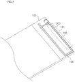
- Figure 1 is a drawing illustrating a perspective view of an internal antenna for a wide band according to an embodiment of the present invention
- Figure 2 is a drawing illustrating a perspective view of the internal antenna for a wide band according to an embodiment of the present invention seen from another direction
- Figure 3 is a drawing illustrating a plan view of the internal antenna for a wide band according to an embodiment of the present invention.
- an internal antenna providing impedance matching for a wide band may comprise a substrate 100, a feeding point 102, an impedance matching/feeding unit 104, a ground pin 106, a radiator 108, and a feeding pin 110.
- the impedance matching/feeding unit 104 comprises a feeding member 200 and a ground member 300.
- RF signals are input to the feeding point 102, and the feeding pin 110 is electrically connected to the feeding point 102 to be formed perpendicularly on the substrate.
- the ground pin 106 is structured to be electrically connected to the ground of a terminal and to be formed perpendicular to the substrate.
- the impedance matching/feeding unit 104 comprises a feeding member 200 that is electrically connected to the feeding pin 110 and is formed perpendicular to the substrate 100 in a designated length, and a ground member 300 that is electrically connected to the ground pin 106 and is placed perpendicular to the substrate 100 in a designated length.
- FIG. 1 to 3 illustrate an example in which the feeding member 200 and ground member 300 have linear forms
- the forms of the feeding member and ground member are not thus limited and can be of a variety of types.
- Other forms for the feeding member and ground member will be described with reference to other drawings.
- the feeding member 200 and the ground member 300 that compose an impedance matching/feeding unit are placed apart at a designated distance.
- a conventional planar inverted-F antenna has a radiator joined perpendicularly to a feeding pin and a ground pin, but an internal antenna providing impedance matching for a wide band according to an embodiment of the present invention additionally comprises a ground member 300 extending from a ground pin and a feeding member 200 extending from a feeding pin, where the feeding member 200 and the ground member 300 perform coupling feeding and impedance matching for a wide band.
- RF signals provided from the feeding pin to the feeding member 200 are coupled to a ground member 300 that is separated at a designated distance, and the coupling thus achieved in a region of a designated length enables impedance matching for a wider band than does the conventional planar inverted-F antenna.
- the length of the feeding member 200 and the ground member 300 for impedance matching for a wide band may be set at approximately 0.1 wavelength, but it may be adjusted according to the frequency band and operating frequency.
- coupling feeding whereby RF signals are transferred by coupling from the feeding member 200 to the ground member 300 is achieved at the impedance matching/feeding unit.
- FIGS 1 and 2 illustrate examples in which the feeding member 200 is formed higher than the ground member 300
- the feeding member 200 and the ground member 300 may also be formed at the same height and facing each other, or the ground member 300 may be formed higher than the feeding member 200.
- the height of the feeding member 200 and of the ground member 300 may be adjusted accordingly.
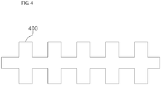
- Figure 4 is a drawing illustrating the shape of a feeding member and a ground member according to another embodiment of the present invention.
- a ground member or a feeding member may be used that have multiple protrusions 400 on the topside and underside of a linear form, different from the linear form illustrated in Figures 1 to 3 .
- feeding member and the ground member may be implemented in a variety of forms, besides the form illustrated in Figure 4 , as long as it is a structure capable of inducing coupling within a region having a designated length.
- the radiator 108 extends from the ground member 300. While Figures 1 and 2 illustrate an example in which the radiator 108 extends from the ground member 300 perpendicularly and then bends to be parallel with the substrate, the form of the radiator is not thus limited, and various forms may be used.
- the length of the radiator 108 is set according to the frequency band used, and its type may also be set in a wide variety. While Figures 2 and 3 illustrate an "L" shaped configuration in which the portion of the radiator parallel to the substrate is bent once, a person skilled in the art would appreciate that such cases in which the portion parallel to the substrate is implemented in linear and meandering forms may also fall within the scope of the present invention.
- radiator 108 receives feed by way of coupling feed, and hence extends from the ground member.
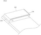
- Figure 5 is a drawing illustrating an example of an antenna carrier to which an antenna according to an embodiment of the present invention is joined.
- an antenna carrier to which an antenna according to an embodiment of the present invention is joined may comprise a flat upper part 500 and multiple wall parts 502, 504, and 506.
- the flat upper part 500 is the part to which the radiator of the antenna is joined, and has a designated area.
- the multiple wall parts 502, 504 and 506 support the flat upper part 500, and are joined to the substrate.
- the feeding member 200 and the ground member 300 of the impedance matching/feeding unit are joined to a first wall part 502, which is relatively longer among the multiple wall parts 502, 504 and 506, while the second wall part 504 and the third wall part 506 provide support together with the first wall part 502.
- Figure 6 is a drawing illustrating a perspective view of an antenna according to an embodiment of the present invention joined to the antenna carrier illustrated in Figure 5
- Figure 7 is a drawing illustrating a perspective view of an antenna according to an embodiment of the present invention joined to the antenna carrier illustrated in Figure 5 seen from another direction.
- Figure 8 is a drawing illustrating a front view of the first side of a wall part of the carrier in an antenna according to an embodiment of the present invention
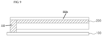
- Figure 9 is a drawing illustrating the reverse side of the first side of a wall part of the carrier in an antenna according to an embodiment of the present invention.
- the antenna carrier is joined to the substrate, and the wall parts 502, 504 and 506 are joined to an upper part of the substrate.
- the ground pin 106 extending perpendicularly from the substrate is formed perpendicularly along a first surface 502a of the first wall part 502, and the ground member 300 extends from the ground pin 106 to be formed on the first surface 502a of the first wall part 502.
- the radiator 108 extends perpendicularly from the ground member 300.
- the feeding pin 110 extending perpendicularly from the substrate and the feeding member 200 extending from the feeding pin 110 are joined to the second surface 502b of the first wall part 502, opposite the first surface 502a.
- the feeding member 200 and the ground member 300 are separated at a designated distance with the first wall part 502 in between; the ground member 300 is joined to the first surface 502a of the first wall part 502, and the feeding member 200 is joined to the second surface 502b of the first wall part 502; and the separating distance between the ground member 300 and the feeding member 200 corresponds to the thickness of the first wall part 502.
- the present invention utilizes both surfaces of the wall part of the carrier, in order to implement a structure for impedance matching for a wide band using coupling between the feeding member 200 and the ground member 300.
- the structure having elements for impedance matching and feeding formed on both surfaces of a wall part of the carrier can provide a smaller size for an antenna than does a conventional structure that has elements for feeding and impedance matching formed on the flat upper side of the carrier.
- the radiator 108 extending from the first wall part 502 is joined to the flat upper part 500 of the carrier.
Landscapes
- Physics & Mathematics (AREA)
- Electromagnetism (AREA)
- Engineering & Computer Science (AREA)
- Computer Networks & Wireless Communication (AREA)
- Details Of Aerials (AREA)
- Waveguide Aerials (AREA)
Description
- The present invention relates to an antenna, more particularly to an internal antenna providing impedance matching for a wide band.
- Recently there has been a demand for the ability to receive mobile communication services of different frequency bands through one mobile communication terminal, even as mobile communication terminals become smaller and lighter. There is a demand for terminals that are able to use signals of multiple bands simultaneously as necessary, for mobile communication services using a variety of frequency bands such as, for example, the CDMA service of the 824-894 MHz band and the PCS service of the 1750-1870 MHz, which have been commercialized in Korea, the CDMA service of the 832-925 MHz band, which has been commercialized in Japan, the PCS service of the 1850-1990 MHz band, which has been commercialized in the U.S., the GSM service of the 880-960 MHz band, which has been commercialized in Europe and China, and the DCS service of the 1710-1880 MHz band, which has been commercialized in parts of Europe; for accommodating such multiple bands there is a demand for an antenna having wide band characteristics.
- Besides these, there is also a demand for composite terminals that are able to use services such as Bluetooth, ZigBee, wireless LAN, GPS, etc. In such a terminal for using services of multiple bands, a multiple band antenna should be used that is able to operate in two or more bands. For an antenna of a generally used mobile communication terminal, a helical antenna and a planar inverted-F antenna (PIFA) are mainly used.
- Here, a helical antenna is an external antenna affixed to the top end of a terminal, and is used together with a monopole antenna. A helical and monopole antenna in combined usage is such that if the antenna is extended out of the body of the terminal, it acts as a monopole antenna, and if it is retracted, it acts as a λ/4 helical antenna. Such an antenna has the advantage of high profits, but due to its non-directivity, the SAR (specific absorption rate) -the standard for the level of harmfulness of electromagnetic waves to the human body- is not good. Also, as a helical antenna is constructed as protruding out of a terminal, it is not easy to provide an esthetic appearance and an external design suitable to portability of the terminal, and no study has been done on an internal structure with regards to this.
- An inverted-F antenna is an antenna designed with a low profile structure for the purpose of overcoming such disadvantages. An inverted-F antenna has a directivity that improves its SAR by reducing the beams emitted towards the human body, left over from the beams going toward the ground, out of all the beams generated by the current left in the radiating part, while at the same time strengthening the beams left to go in the direction of the radiating part; and it may also be implemented as a low profile structure operating with a square micro-strip antenna, the length of the rectangular flat-board radiating part being reduced in half.
- Since such an inverted-F antenna has radiating characteristics with a directivity that reduces the strength of beams going toward the human body and fortifies the strength of the beams going outward from the body, it has a superior electromagnetic specific absorption rate when compared with a helical antenna. However, an inverted-F antenna has the problem of having a narrow frequency band width.
- The narrow frequency band width of an inverted-F antenna is due to point-matching, in which the matching with a radiator takes place at a specific point.
- In order to overcome the problem related to a narrow band width due to point matching, an application was submitted for a Korean patent by the inventor, and this application presents a structure that overcomes the problem of a narrow band width of the existing inverted-F antenna by means of coupling matching and coupling feeding in a comparatively long interval.
- However, there was the problem of the size of the antenna being large, as a separate impedance matching part for such coupling matching and coupling feeding occupied a comparatively large space.
EP 2242144 A2 discloses a multi band internal antenna that may include a board, an impedance matching/feeding part formed on the board, and a first radiation element joined to the impedance matching/feeding part. The proposed impedance matching/feeding part may include: a first matching element of a particular length that is coupled to a ground, and a second matching element of a particular length that is arranged with a distance from the first matching element and is electrically coupled to a feeding point. The distance between the proposed first matching element and the proposed second matching element may vary partially. The proposed multi band internal antenna can utilize capacitive coupling matching to achieve wide-band characteristics even for multi-band designs.
EP0814535 A2 discloses a surface-mount antenna including a radiation electrode formed on one or more surfaces of a rectangular parallelopiped base member comprising a dielectric or a magnetic substance so as to have one end as an open end and another end as a first ground electrode, a feeding electrode formed on the surface or surfaces, and a second ground electrode formed in proximity to the open end of said radiation electrode.
US 2004/169606 A1 discloses a surface-mount type antenna including a substantially prismatic base body, feeding and ground terminals formed on one side surface of the base body; and a radiating electrode, to one end of which is connected the ground terminal, disposed such that its other end extends from one side surface, through another end side part of one principal surface of the base body, to the one end side part thereof, then turns to the other end side part, and is eventually formed into an open end located near the other end side part. The proposed feeding terminal is disposed near the radiating electrode. The proposed antenna apparatus is constructed by mounting the surface-mount type antenna on the mounting substrate having the feeding electrode, the ground electrode, and the ground conductor layer. - To resolve the problem of the related art addressed above, an aspect of the invention provides an internal antenna for a wide band for the purpose of overcoming the narrow band problem of a planar inverted-F antenna.
- Another purpose of the present invention is to provide an internal antenna for a wide band that utilizes space more efficiently than an internal antenna for a wide band that uses coupling matching and coupling feeding.
- Other purposes of the present invention can readily be derived by those skilled in the art from the embodiments below.
- To achieve the objective above, an aspect of the invention provides an internal antenna providing impedance matching for a wide band that includes a substrate; an impedance matching/feeding unit comprising a feeding member, separated from the substrate at a designated distance, configured to receive RF signals, and of a designated length in a first direction, and a ground member, separated from the substrate at a designated distance, separated from the feeding member at a designated distance in a second direction perpendicular to the first direction, and of a designated length in the first direction; and a radiator extending from the ground member; wherein the impedance matching/feeding unit performs impedance matching by way of coupling between the feeding member and the ground member, and the radiator receives coupling feeding from the feeding member.
- The antenna may further include a feeding pin that is perpendicular to the substrate and electrically connected to a feeding point and the feeding member.
- The antenna may further include a ground pin that is perpendicular to the substrate and electrically connected to a ground and the ground member.
- The length of the ground member and feeding member in the first direction should preferably be approximately 0.1 of the wavelength.
- The antenna may further include a carrier that is secured by the joining of the feeding member, ground member and radiator.
- The carrier comprises a flat upper part and multiple wall parts, and the multiple wall parts are joined to the substrate.
- The feeding member is joined to one side of one of the multiple wall parts, and the ground member is joined to the opposite side of the one side and separated at a designated distance.
- Another aspect of the invention provides an internal antenna providing impedance matching for a wide band that includes a substrate; a carrier joined to the substrate; an impedance matching/feeding unit that includes a ground member joined to a first surface of one of the wall parts of the carrier and electrically connected to the ground, and a feeding member joined to a second surface opposite the first surface and configured to receive feed of RF signals; and a radiator extending from the ground and joined to the carrier.
- An embodiment of the present invention offers the advantages of overcoming the narrow band problem of a planar inverted-F antenna, and of allowing more efficient utilization of space in an internal antenna.
-
-
Figure 1 is a drawing illustrating a perspective view of an internal antenna for a wide band according to an embodiment of the present invention. -
Figure 2 is a drawing illustrating a perspective view of the internal antenna for a wide band according to an embodiment of the present invention seen from another direction. -
Figure 3 is a drawing illustrating a plan view of the internal antenna for a wide band according to an embodiment of the present invention. -
Figure 4 is a drawing illustrating the shape of a feeding member and a ground member according to another embodiment of the present invention. -
Figure 5 is a drawing illustrating an example of an antenna carrier joined to an antenna according to an embodiment of the present invention. -
Figure 6 is a drawing illustrating a perspective view of an antenna according to an embodiment of the present invention joined to the antenna carrier illustrated inFigure 5 . -
Figure 7 is a drawing illustrating a perspective view of an antenna according to an embodiment of the present invention joined to the antenna carrier illustrated inFigure 5 seen from another direction. -
Figure 8 is a drawing illustrating a front view of the first side of a wall part of the carrier in an antenna according to an embodiment of the present invention. -
Figure 9 is a drawing illustrating the reverse side of the first side of a wall part of the carrier in an antenna according to an embodiment of the present invention. - An internal antenna providing impedance matching for a wide band according to an embodiment of the invention will be described below in more detail with reference to the accompanying drawings.
- An internal antenna providing impedance matching for a wide band according to an embodiment of the invention may be implemented with the use of a carrier, but for the sake of ease of explanation, first a description will be given of an antenna having a structure without a carrier with reference to
Figures 1 to 3 , and then later a description will be given of a structure implemented with a carrier. -
Figure 1 is a drawing illustrating a perspective view of an internal antenna for a wide band according to an embodiment of the present invention;Figure 2 is a drawing illustrating a perspective view of the internal antenna for a wide band according to an embodiment of the present invention seen from another direction; andFigure 3 is a drawing illustrating a plan view of the internal antenna for a wide band according to an embodiment of the present invention. - Referring to
Figures 1 to 3 , an internal antenna providing impedance matching for a wide band according to an embodiment of the present invention may comprise asubstrate 100, afeeding point 102, an impedance matching/feeding unit 104, aground pin 106, aradiator 108, and afeeding pin 110. Also, the impedance matching/feeding unit 104 comprises afeeding member 200 and aground member 300. - RF signals are input to the
feeding point 102, and thefeeding pin 110 is electrically connected to thefeeding point 102 to be formed perpendicularly on the substrate. Theground pin 106 is structured to be electrically connected to the ground of a terminal and to be formed perpendicular to the substrate. - The impedance matching/
feeding unit 104 comprises afeeding member 200 that is electrically connected to thefeeding pin 110 and is formed perpendicular to thesubstrate 100 in a designated length, and aground member 300 that is electrically connected to theground pin 106 and is placed perpendicular to thesubstrate 100 in a designated length. - Whereas
Figures 1 to 3 illustrate an example in which thefeeding member 200 andground member 300 have linear forms, the forms of the feeding member and ground member are not thus limited and can be of a variety of types. Other forms for the feeding member and ground member will be described with reference to other drawings. - As illustrated in
Figure 3 , thefeeding member 200 and theground member 300 that compose an impedance matching/feeding unit are placed apart at a designated distance. - A conventional planar inverted-F antenna has a radiator joined perpendicularly to a feeding pin and a ground pin, but an internal antenna providing impedance matching for a wide band according to an embodiment of the present invention additionally comprises a
ground member 300 extending from a ground pin and afeeding member 200 extending from a feeding pin, where thefeeding member 200 and theground member 300 perform coupling feeding and impedance matching for a wide band. - RF signals provided from the feeding pin to the feeding
member 200 are coupled to aground member 300 that is separated at a designated distance, and the coupling thus achieved in a region of a designated length enables impedance matching for a wider band than does the conventional planar inverted-F antenna. - The length of the feeding
member 200 and theground member 300 for impedance matching for a wide band may be set at approximately 0.1 wavelength, but it may be adjusted according to the frequency band and operating frequency. - Also, coupling feeding whereby RF signals are transferred by coupling from the feeding
member 200 to theground member 300 is achieved at the impedance matching/feeding unit. - Whereas
Figures 1 and2 illustrate examples in which the feedingmember 200 is formed higher than theground member 300, the feedingmember 200 and theground member 300 may also be formed at the same height and facing each other, or theground member 300 may be formed higher than the feedingmember 200. - In other words, depending on the amount of coupling required, the height of the feeding
member 200 and of theground member 300 may be adjusted accordingly. -
Figure 4 is a drawing illustrating the shape of a feeding member and a ground member according to another embodiment of the present invention. - Referring to
Figure 4 , a ground member or a feeding member may be used that havemultiple protrusions 400 on the topside and underside of a linear form, different from the linear form illustrated inFigures 1 to 3 . - By adding
multiple protrusions 400 to a line form in this manner, even greater capacitance, necessary for coupling, may be obtained, and by means of this, impedance matching for a wider band may be performed. Also, the capacitance value has to be varied for impedance matching over a wider band, and the linear structure having protrusions on the topside and underside as inFigure 4 can provide such varying of capacitance for coupling. - Of course, a person skilled in the art would appreciate that the feeding member and the ground member may be implemented in a variety of forms, besides the form illustrated in
Figure 4 , as long as it is a structure capable of inducing coupling within a region having a designated length. - The
radiator 108 extends from theground member 300. WhileFigures 1 and2 illustrate an example in which theradiator 108 extends from theground member 300 perpendicularly and then bends to be parallel with the substrate, the form of the radiator is not thus limited, and various forms may be used. - The length of the
radiator 108 is set according to the frequency band used, and its type may also be set in a wide variety. WhileFigures 2 and3 illustrate an "L" shaped configuration in which the portion of the radiator parallel to the substrate is bent once, a person skilled in the art would appreciate that such cases in which the portion parallel to the substrate is implemented in linear and meandering forms may also fall within the scope of the present invention. - Whereas in an ordinary planar inverted-F antenna, a radiator is electrically connected to a feeding pin since it receives direct feed, in an antenna according to an embodiment of the present invention, the
radiator 108 receives feed by way of coupling feed, and hence extends from the ground member. -
Figure 5 is a drawing illustrating an example of an antenna carrier to which an antenna according to an embodiment of the present invention is joined. - Referring to
Figure 5 , an antenna carrier to which an antenna according to an embodiment of the present invention is joined may comprise a flatupper part 500 andmultiple wall parts - The flat
upper part 500 is the part to which the radiator of the antenna is joined, and has a designated area. - The
multiple wall parts upper part 500, and are joined to the substrate. The feedingmember 200 and theground member 300 of the impedance matching/feeding unit are joined to afirst wall part 502, which is relatively longer among themultiple wall parts second wall part 504 and thethird wall part 506 provide support together with thefirst wall part 502. -
Figure 6 is a drawing illustrating a perspective view of an antenna according to an embodiment of the present invention joined to the antenna carrier illustrated inFigure 5 , andFigure 7 is a drawing illustrating a perspective view of an antenna according to an embodiment of the present invention joined to the antenna carrier illustrated inFigure 5 seen from another direction. Also,Figure 8 is a drawing illustrating a front view of the first side of a wall part of the carrier in an antenna according to an embodiment of the present invention, andFigure 9 is a drawing illustrating the reverse side of the first side of a wall part of the carrier in an antenna according to an embodiment of the present invention. - Referring to
Figures 6 and7 , the antenna carrier is joined to the substrate, and thewall parts - Referring to
Figure 8 , theground pin 106 extending perpendicularly from the substrate is formed perpendicularly along afirst surface 502a of thefirst wall part 502, and theground member 300 extends from theground pin 106 to be formed on thefirst surface 502a of thefirst wall part 502. - Also, the
radiator 108 extends perpendicularly from theground member 300. - At the same time, referring to
Figure 9 , thefeeding pin 110 extending perpendicularly from the substrate and the feedingmember 200 extending from thefeeding pin 110 are joined to thesecond surface 502b of thefirst wall part 502, opposite thefirst surface 502a. - In other words, the feeding
member 200 and theground member 300 are separated at a designated distance with thefirst wall part 502 in between; theground member 300 is joined to thefirst surface 502a of thefirst wall part 502, and the feedingmember 200 is joined to thesecond surface 502b of thefirst wall part 502; and the separating distance between theground member 300 and the feedingmember 200 corresponds to the thickness of thefirst wall part 502. - The present invention utilizes both surfaces of the wall part of the carrier, in order to implement a structure for impedance matching for a wide band using coupling between the feeding
member 200 and theground member 300. - In this manner, the structure having elements for impedance matching and feeding formed on both surfaces of a wall part of the carrier can provide a smaller size for an antenna than does a conventional structure that has elements for feeding and impedance matching formed on the flat upper side of the carrier.
- The
radiator 108 extending from thefirst wall part 502 is joined to the flatupper part 500 of the carrier.
Claims (3)
- An internal antenna providing impedance matching for a wide band, comprising:a substrate (100);a carrier joined on the substrate (100),
the carrier comprising one or more wall parts (502, 504, 506);an impedance matching/feeding unit (104)
comprising a ground member (300) and a feeding member (200),
wherein the impedance matching/feeding unit (104) performs impedance matching by way of capacitive coupling; anda radiator (108) extending from the ground member (300) and joined to the carrier,characterized in thatthe ground member (300) is joined to a first surface of one of wall parts (502, 504, 506) of the carrier and electrically connected to a ground, and in thatthe feeding member (200) is joined to a second surface opposite the first surface on the same wall part and is configured to receive a feed of RF signals. - The internal antenna providing impedance matching for a wide band according to claim 1, comprising a ground pin (106), a feeding pin (110) and a feeding point (102),
wherein the first surface has the ground pin (106) joined thereto,
the ground pin (106) electrically connectable to a ground and formed perpendicularly from the substrate (100) to be connected to the ground member (300), and
the second surface has the feeding pin (110) joined thereto,
the feeding pin (110) electrically connected to the feeding point (102) and formed perpendicularly from the substrate (100) to be connected to the feeding member (200). - The internal antenna providing impedance matching for a wide band according to one of claims 1 or 2,
wherein the carrier is equipped with a flat upper part (500) formed over an upper part of the wall parts (502, 504, 506), and
the radiator (108) extends from the ground member (300) to be formed over the flat upper part (500).
Applications Claiming Priority (2)
| Application Number | Priority Date | Filing Date | Title |
|---|---|---|---|
| KR20080125477 | 2008-12-10 | ||
| PCT/KR2009/001599 WO2010067924A1 (en) | 2008-12-10 | 2009-03-30 | Internal antenna supporting wideband impedance matching |
Publications (3)
| Publication Number | Publication Date |
|---|---|
| EP2369675A1 EP2369675A1 (en) | 2011-09-28 |
| EP2369675A4 EP2369675A4 (en) | 2017-06-28 |
| EP2369675B1 true EP2369675B1 (en) | 2018-08-29 |
Family
ID=42242898
Family Applications (1)
| Application Number | Title | Priority Date | Filing Date |
|---|---|---|---|
| EP09832011.2A Not-in-force EP2369675B1 (en) | 2008-12-10 | 2009-03-30 | Internal antenna supporting wideband impedance matching |
Country Status (6)
| Country | Link |
|---|---|
| US (1) | US8743011B2 (en) |
| EP (1) | EP2369675B1 (en) |
| JP (1) | JP2012511857A (en) |
| KR (2) | KR101075095B1 (en) |
| CN (1) | CN102246347A (en) |
| WO (1) | WO2010067924A1 (en) |
Families Citing this family (2)
| Publication number | Priority date | Publication date | Assignee | Title |
|---|---|---|---|---|
| TW201345050A (en) * | 2012-04-27 | 2013-11-01 | Univ Nat Taiwan Science Tech | Dual band antenna with circular polarization |
| US10090596B2 (en) * | 2014-07-10 | 2018-10-02 | Google Llc | Robust antenna configurations for wireless connectivity of smart home devices |
Family Cites Families (9)
| Publication number | Priority date | Publication date | Assignee | Title |
|---|---|---|---|---|
| JP3114621B2 (en) | 1996-06-19 | 2000-12-04 | 株式会社村田製作所 | Surface mount antenna and communication device using the same |
| KR100533624B1 (en) * | 2002-04-16 | 2005-12-06 | 삼성전기주식회사 | Multi band chip antenna with dual feeding port, and mobile communication apparatus using the same |
| US6774850B2 (en) * | 2002-09-18 | 2004-08-10 | High Tech Computer, Corp. | Broadband couple-fed planar antennas with coupled metal strips on the ground plane |
| JP3739740B2 (en) * | 2002-11-28 | 2006-01-25 | 京セラ株式会社 | Surface mount antenna and antenna device |
| FI116332B (en) | 2002-12-16 | 2005-10-31 | Lk Products Oy | Antenna for a flat radio |
| JP4102411B2 (en) * | 2006-04-13 | 2008-06-18 | 株式会社東芝 | Mobile communication terminal |
| KR101442503B1 (en) * | 2006-11-16 | 2014-09-24 | 갈트로닉스 코포레이션 리미티드 | Compact antenna |
| KR100799875B1 (en) * | 2006-11-22 | 2008-01-30 | 삼성전기주식회사 | Chip antenna and mobile terminal including the same |
| WO2009088231A2 (en) * | 2008-01-08 | 2009-07-16 | Ace Antenna Corp. | Multi-band internal antenna |
-
2009
- 2009-03-25 KR KR1020090025436A patent/KR101075095B1/en not_active Expired - Fee Related
- 2009-03-30 JP JP2011540587A patent/JP2012511857A/en active Pending
- 2009-03-30 CN CN2009801495780A patent/CN102246347A/en active Pending
- 2009-03-30 WO PCT/KR2009/001599 patent/WO2010067924A1/en not_active Ceased
- 2009-03-30 US US13/133,582 patent/US8743011B2/en not_active Expired - Fee Related
- 2009-03-30 EP EP09832011.2A patent/EP2369675B1/en not_active Not-in-force
-
2011
- 2011-05-13 KR KR1020110045227A patent/KR101130024B1/en not_active Expired - Fee Related
Non-Patent Citations (1)
| Title |
|---|
| None * |
Also Published As
| Publication number | Publication date |
|---|---|
| KR101130024B1 (en) | 2012-03-28 |
| KR20100067008A (en) | 2010-06-18 |
| WO2010067924A1 (en) | 2010-06-17 |
| EP2369675A1 (en) | 2011-09-28 |
| US8743011B2 (en) | 2014-06-03 |
| KR20110057109A (en) | 2011-05-31 |
| KR101075095B1 (en) | 2011-10-19 |
| JP2012511857A (en) | 2012-05-24 |
| US20110241963A1 (en) | 2011-10-06 |
| EP2369675A4 (en) | 2017-06-28 |
| CN102246347A (en) | 2011-11-16 |
Similar Documents
| Publication | Publication Date | Title |
|---|---|---|
| US8884836B2 (en) | Multi-band internal antenna | |
| KR100980218B1 (en) | Internal Antenna Providing Impedance Maching for Multi Band | |
| CN1871744B (en) | Planar inverte F antennas including current nulls between feed and ground couplings and related communications devices | |
| KR101171421B1 (en) | Wide Band Antenna Using Coupling Matching | |
| KR101103208B1 (en) | Broadband Antenna with Coupling Matching with Shorted Radiator Termination | |
| KR20110109383A (en) | Broadband embedded antenna with electromagnetic coupling for improved impedance matching | |
| JP2014011796A (en) | Antenna and manufacturing method thereof | |
| US20120044122A1 (en) | Broadband antenna using an electric loop-type signal line | |
| US8810469B2 (en) | Built-in antenna which supports broadband impedance matching and has feeding patch coupled to substrate | |
| KR20050003341A (en) | Internal antenna of mobile handset | |
| EP2369675A1 (en) | Internal antenna supporting wideband impedance matching | |
| WO2011046368A2 (en) | Broadband built-in antenna using double electromagnetic coupling | |
| KR20090126001A (en) | Portable terminal built-in antenna | |
| KR20100099076A (en) | Ultra wide band monopole internal antenna | |
| KR101090114B1 (en) | Broadband Internal Antenna Using Electromagnetic Coupling | |
| KR101053105B1 (en) | Broadband Antenna Using Tubular Matching | |
| KR20110092861A (en) | Broadband internal antenna using dual electromagnetic coupling | |
| KR100999857B1 (en) | Built-in antenna with small radiator | |
| KR20110040127A (en) | Wideband Impedance Matching Antenna Using Coupling |
Legal Events
| Date | Code | Title | Description |
|---|---|---|---|
| PUAI | Public reference made under article 153(3) epc to a published international application that has entered the european phase |
Free format text: ORIGINAL CODE: 0009012 |
|
| 17P | Request for examination filed |
Effective date: 20110609 |
|
| AK | Designated contracting states |
Kind code of ref document: A1 Designated state(s): AT BE BG CH CY CZ DE DK EE ES FI FR GB GR HR HU IE IS IT LI LT LU LV MC MK MT NL NO PL PT RO SE SI SK TR |
|
| DAX | Request for extension of the european patent (deleted) | ||
| RAP1 | Party data changed (applicant data changed or rights of an application transferred) |
Owner name: ACE TECHNOLOGIES CORPORATION |
|
| RA4 | Supplementary search report drawn up and despatched (corrected) |
Effective date: 20170531 |
|
| RIC1 | Information provided on ipc code assigned before grant |
Ipc: H01Q 1/24 20060101ALI20170524BHEP Ipc: H01Q 5/50 20150101ALI20170524BHEP Ipc: H01Q 1/38 20060101AFI20170524BHEP Ipc: H01Q 9/04 20060101ALI20170524BHEP |
|
| GRAP | Despatch of communication of intention to grant a patent |
Free format text: ORIGINAL CODE: EPIDOSNIGR1 |
|
| STAA | Information on the status of an ep patent application or granted ep patent |
Free format text: STATUS: GRANT OF PATENT IS INTENDED |
|
| INTG | Intention to grant announced |
Effective date: 20180319 |
|
| GRAS | Grant fee paid |
Free format text: ORIGINAL CODE: EPIDOSNIGR3 |
|
| GRAA | (expected) grant |
Free format text: ORIGINAL CODE: 0009210 |
|
| STAA | Information on the status of an ep patent application or granted ep patent |
Free format text: STATUS: THE PATENT HAS BEEN GRANTED |
|
| AK | Designated contracting states |
Kind code of ref document: B1 Designated state(s): AT BE BG CH CY CZ DE DK EE ES FI FR GB GR HR HU IE IS IT LI LT LU LV MC MK MT NL NO PL PT RO SE SI SK TR |
|
| REG | Reference to a national code |
Ref country code: GB Ref legal event code: FG4D |
|
| REG | Reference to a national code |
Ref country code: CH Ref legal event code: EP |
|
| REG | Reference to a national code |
Ref country code: AT Ref legal event code: REF Ref document number: 1036247 Country of ref document: AT Kind code of ref document: T Effective date: 20180915 |
|
| REG | Reference to a national code |
Ref country code: IE Ref legal event code: FG4D |
|
| REG | Reference to a national code |
Ref country code: DE Ref legal event code: R096 Ref document number: 602009054217 Country of ref document: DE |
|
| REG | Reference to a national code |
Ref country code: NL Ref legal event code: MP Effective date: 20180829 |
|
| REG | Reference to a national code |
Ref country code: LT Ref legal event code: MG4D |
|
| PG25 | Lapsed in a contracting state [announced via postgrant information from national office to epo] |
Ref country code: NL Free format text: LAPSE BECAUSE OF FAILURE TO SUBMIT A TRANSLATION OF THE DESCRIPTION OR TO PAY THE FEE WITHIN THE PRESCRIBED TIME-LIMIT Effective date: 20180829 Ref country code: BG Free format text: LAPSE BECAUSE OF FAILURE TO SUBMIT A TRANSLATION OF THE DESCRIPTION OR TO PAY THE FEE WITHIN THE PRESCRIBED TIME-LIMIT Effective date: 20181129 Ref country code: NO Free format text: LAPSE BECAUSE OF FAILURE TO SUBMIT A TRANSLATION OF THE DESCRIPTION OR TO PAY THE FEE WITHIN THE PRESCRIBED TIME-LIMIT Effective date: 20181129 Ref country code: SE Free format text: LAPSE BECAUSE OF FAILURE TO SUBMIT A TRANSLATION OF THE DESCRIPTION OR TO PAY THE FEE WITHIN THE PRESCRIBED TIME-LIMIT Effective date: 20180829 Ref country code: IS Free format text: LAPSE BECAUSE OF FAILURE TO SUBMIT A TRANSLATION OF THE DESCRIPTION OR TO PAY THE FEE WITHIN THE PRESCRIBED TIME-LIMIT Effective date: 20181229 Ref country code: LT Free format text: LAPSE BECAUSE OF FAILURE TO SUBMIT A TRANSLATION OF THE DESCRIPTION OR TO PAY THE FEE WITHIN THE PRESCRIBED TIME-LIMIT Effective date: 20180829 Ref country code: GR Free format text: LAPSE BECAUSE OF FAILURE TO SUBMIT A TRANSLATION OF THE DESCRIPTION OR TO PAY THE FEE WITHIN THE PRESCRIBED TIME-LIMIT Effective date: 20181130 Ref country code: FI Free format text: LAPSE BECAUSE OF FAILURE TO SUBMIT A TRANSLATION OF THE DESCRIPTION OR TO PAY THE FEE WITHIN THE PRESCRIBED TIME-LIMIT Effective date: 20180829 |
|
| REG | Reference to a national code |
Ref country code: AT Ref legal event code: MK05 Ref document number: 1036247 Country of ref document: AT Kind code of ref document: T Effective date: 20180829 |
|
| PG25 | Lapsed in a contracting state [announced via postgrant information from national office to epo] |
Ref country code: LV Free format text: LAPSE BECAUSE OF FAILURE TO SUBMIT A TRANSLATION OF THE DESCRIPTION OR TO PAY THE FEE WITHIN THE PRESCRIBED TIME-LIMIT Effective date: 20180829 Ref country code: ES Free format text: LAPSE BECAUSE OF FAILURE TO SUBMIT A TRANSLATION OF THE DESCRIPTION OR TO PAY THE FEE WITHIN THE PRESCRIBED TIME-LIMIT Effective date: 20180829 Ref country code: HR Free format text: LAPSE BECAUSE OF FAILURE TO SUBMIT A TRANSLATION OF THE DESCRIPTION OR TO PAY THE FEE WITHIN THE PRESCRIBED TIME-LIMIT Effective date: 20180829 |
|
| PG25 | Lapsed in a contracting state [announced via postgrant information from national office to epo] |
Ref country code: RO Free format text: LAPSE BECAUSE OF FAILURE TO SUBMIT A TRANSLATION OF THE DESCRIPTION OR TO PAY THE FEE WITHIN THE PRESCRIBED TIME-LIMIT Effective date: 20180829 Ref country code: EE Free format text: LAPSE BECAUSE OF FAILURE TO SUBMIT A TRANSLATION OF THE DESCRIPTION OR TO PAY THE FEE WITHIN THE PRESCRIBED TIME-LIMIT Effective date: 20180829 Ref country code: IT Free format text: LAPSE BECAUSE OF FAILURE TO SUBMIT A TRANSLATION OF THE DESCRIPTION OR TO PAY THE FEE WITHIN THE PRESCRIBED TIME-LIMIT Effective date: 20180829 Ref country code: AT Free format text: LAPSE BECAUSE OF FAILURE TO SUBMIT A TRANSLATION OF THE DESCRIPTION OR TO PAY THE FEE WITHIN THE PRESCRIBED TIME-LIMIT Effective date: 20180829 Ref country code: PL Free format text: LAPSE BECAUSE OF FAILURE TO SUBMIT A TRANSLATION OF THE DESCRIPTION OR TO PAY THE FEE WITHIN THE PRESCRIBED TIME-LIMIT Effective date: 20180829 Ref country code: CZ Free format text: LAPSE BECAUSE OF FAILURE TO SUBMIT A TRANSLATION OF THE DESCRIPTION OR TO PAY THE FEE WITHIN THE PRESCRIBED TIME-LIMIT Effective date: 20180829 |
|
| PG25 | Lapsed in a contracting state [announced via postgrant information from national office to epo] |
Ref country code: SK Free format text: LAPSE BECAUSE OF FAILURE TO SUBMIT A TRANSLATION OF THE DESCRIPTION OR TO PAY THE FEE WITHIN THE PRESCRIBED TIME-LIMIT Effective date: 20180829 Ref country code: DK Free format text: LAPSE BECAUSE OF FAILURE TO SUBMIT A TRANSLATION OF THE DESCRIPTION OR TO PAY THE FEE WITHIN THE PRESCRIBED TIME-LIMIT Effective date: 20180829 |
|
| REG | Reference to a national code |
Ref country code: DE Ref legal event code: R097 Ref document number: 602009054217 Country of ref document: DE |
|
| PLBE | No opposition filed within time limit |
Free format text: ORIGINAL CODE: 0009261 |
|
| STAA | Information on the status of an ep patent application or granted ep patent |
Free format text: STATUS: NO OPPOSITION FILED WITHIN TIME LIMIT |
|
| 26N | No opposition filed |
Effective date: 20190531 |
|
| PG25 | Lapsed in a contracting state [announced via postgrant information from national office to epo] |
Ref country code: SI Free format text: LAPSE BECAUSE OF FAILURE TO SUBMIT A TRANSLATION OF THE DESCRIPTION OR TO PAY THE FEE WITHIN THE PRESCRIBED TIME-LIMIT Effective date: 20180829 |
|
| REG | Reference to a national code |
Ref country code: DE Ref legal event code: R119 Ref document number: 602009054217 Country of ref document: DE |
|
| PG25 | Lapsed in a contracting state [announced via postgrant information from national office to epo] |
Ref country code: MC Free format text: LAPSE BECAUSE OF FAILURE TO SUBMIT A TRANSLATION OF THE DESCRIPTION OR TO PAY THE FEE WITHIN THE PRESCRIBED TIME-LIMIT Effective date: 20180829 |
|
| REG | Reference to a national code |
Ref country code: CH Ref legal event code: PL |
|
| GBPC | Gb: european patent ceased through non-payment of renewal fee |
Effective date: 20190330 |
|
| PG25 | Lapsed in a contracting state [announced via postgrant information from national office to epo] |
Ref country code: LU Free format text: LAPSE BECAUSE OF NON-PAYMENT OF DUE FEES Effective date: 20190330 |
|
| REG | Reference to a national code |
Ref country code: BE Ref legal event code: MM Effective date: 20190331 |
|
| PG25 | Lapsed in a contracting state [announced via postgrant information from national office to epo] |
Ref country code: DE Free format text: LAPSE BECAUSE OF NON-PAYMENT OF DUE FEES Effective date: 20191001 Ref country code: GB Free format text: LAPSE BECAUSE OF NON-PAYMENT OF DUE FEES Effective date: 20190330 Ref country code: IE Free format text: LAPSE BECAUSE OF NON-PAYMENT OF DUE FEES Effective date: 20190330 Ref country code: CH Free format text: LAPSE BECAUSE OF NON-PAYMENT OF DUE FEES Effective date: 20190331 Ref country code: LI Free format text: LAPSE BECAUSE OF NON-PAYMENT OF DUE FEES Effective date: 20190331 |
|
| PG25 | Lapsed in a contracting state [announced via postgrant information from national office to epo] |
Ref country code: BE Free format text: LAPSE BECAUSE OF NON-PAYMENT OF DUE FEES Effective date: 20190331 Ref country code: FR Free format text: LAPSE BECAUSE OF NON-PAYMENT OF DUE FEES Effective date: 20190331 |
|
| PG25 | Lapsed in a contracting state [announced via postgrant information from national office to epo] |
Ref country code: TR Free format text: LAPSE BECAUSE OF FAILURE TO SUBMIT A TRANSLATION OF THE DESCRIPTION OR TO PAY THE FEE WITHIN THE PRESCRIBED TIME-LIMIT Effective date: 20180829 |
|
| PG25 | Lapsed in a contracting state [announced via postgrant information from national office to epo] |
Ref country code: PT Free format text: LAPSE BECAUSE OF FAILURE TO SUBMIT A TRANSLATION OF THE DESCRIPTION OR TO PAY THE FEE WITHIN THE PRESCRIBED TIME-LIMIT Effective date: 20181229 Ref country code: MT Free format text: LAPSE BECAUSE OF NON-PAYMENT OF DUE FEES Effective date: 20190330 |
|
| PG25 | Lapsed in a contracting state [announced via postgrant information from national office to epo] |
Ref country code: CY Free format text: LAPSE BECAUSE OF FAILURE TO SUBMIT A TRANSLATION OF THE DESCRIPTION OR TO PAY THE FEE WITHIN THE PRESCRIBED TIME-LIMIT Effective date: 20180829 |
|
| PG25 | Lapsed in a contracting state [announced via postgrant information from national office to epo] |
Ref country code: HU Free format text: LAPSE BECAUSE OF FAILURE TO SUBMIT A TRANSLATION OF THE DESCRIPTION OR TO PAY THE FEE WITHIN THE PRESCRIBED TIME-LIMIT; INVALID AB INITIO Effective date: 20090330 |
|
| PG25 | Lapsed in a contracting state [announced via postgrant information from national office to epo] |
Ref country code: MK Free format text: LAPSE BECAUSE OF FAILURE TO SUBMIT A TRANSLATION OF THE DESCRIPTION OR TO PAY THE FEE WITHIN THE PRESCRIBED TIME-LIMIT Effective date: 20180829 |