EP2369628A2 - Programmable III-nitride transistor with aluminum-doped gate - Google Patents
Programmable III-nitride transistor with aluminum-doped gate Download PDFInfo
- Publication number
- EP2369628A2 EP2369628A2 EP11001844A EP11001844A EP2369628A2 EP 2369628 A2 EP2369628 A2 EP 2369628A2 EP 11001844 A EP11001844 A EP 11001844A EP 11001844 A EP11001844 A EP 11001844A EP 2369628 A2 EP2369628 A2 EP 2369628A2
- Authority
- EP
- European Patent Office
- Prior art keywords
- iii
- nitride
- heterojunction device
- modification
- nitride heterojunction
- Prior art date
- Legal status (The legal status is an assumption and is not a legal conclusion. Google has not performed a legal analysis and makes no representation as to the accuracy of the status listed.)
- Withdrawn
Links
Images
Classifications
-
- H—ELECTRICITY
- H10—SEMICONDUCTOR DEVICES; ELECTRIC SOLID-STATE DEVICES NOT OTHERWISE PROVIDED FOR
- H10D—INORGANIC ELECTRIC SEMICONDUCTOR DEVICES
- H10D30/00—Field-effect transistors [FET]
- H10D30/40—FETs having zero-dimensional [0D], one-dimensional [1D] or two-dimensional [2D] charge carrier gas channels
- H10D30/47—FETs having zero-dimensional [0D], one-dimensional [1D] or two-dimensional [2D] charge carrier gas channels having two-dimensional [2D] charge carrier gas channels, e.g. nanoribbon FETs or high electron mobility transistors [HEMT]
- H10D30/471—High electron mobility transistors [HEMT] or high hole mobility transistors [HHMT]
- H10D30/475—High electron mobility transistors [HEMT] or high hole mobility transistors [HHMT] having wider bandgap layer formed on top of lower bandgap active layer, e.g. undoped barrier HEMTs such as i-AlGaN/GaN HEMTs
- H10D30/4755—High electron mobility transistors [HEMT] or high hole mobility transistors [HHMT] having wider bandgap layer formed on top of lower bandgap active layer, e.g. undoped barrier HEMTs such as i-AlGaN/GaN HEMTs having wide bandgap charge-carrier supplying layers, e.g. modulation doped HEMTs such as n-AlGaAs/GaAs HEMTs
-
- H—ELECTRICITY
- H10—SEMICONDUCTOR DEVICES; ELECTRIC SOLID-STATE DEVICES NOT OTHERWISE PROVIDED FOR
- H10D—INORGANIC ELECTRIC SEMICONDUCTOR DEVICES
- H10D30/00—Field-effect transistors [FET]
- H10D30/80—FETs having rectifying junction gate electrodes
- H10D30/801—FETs having heterojunction gate electrodes
- H10D30/803—Programmable transistors, e.g. having charge-trapping quantum well
-
- H—ELECTRICITY
- H10—SEMICONDUCTOR DEVICES; ELECTRIC SOLID-STATE DEVICES NOT OTHERWISE PROVIDED FOR
- H10D—INORGANIC ELECTRIC SEMICONDUCTOR DEVICES
- H10D62/00—Semiconductor bodies, or regions thereof, of devices having potential barriers
- H10D62/80—Semiconductor bodies, or regions thereof, of devices having potential barriers characterised by the materials
- H10D62/85—Semiconductor bodies, or regions thereof, of devices having potential barriers characterised by the materials being Group III-V materials, e.g. GaAs
- H10D62/8503—Nitride Group III-V materials, e.g. AlN or GaN
-
- H—ELECTRICITY
- H10—SEMICONDUCTOR DEVICES; ELECTRIC SOLID-STATE DEVICES NOT OTHERWISE PROVIDED FOR
- H10D—INORGANIC ELECTRIC SEMICONDUCTOR DEVICES
- H10D62/00—Semiconductor bodies, or regions thereof, of devices having potential barriers
- H10D62/80—Semiconductor bodies, or regions thereof, of devices having potential barriers characterised by the materials
- H10D62/85—Semiconductor bodies, or regions thereof, of devices having potential barriers characterised by the materials being Group III-V materials, e.g. GaAs
- H10D62/854—Semiconductor bodies, or regions thereof, of devices having potential barriers characterised by the materials being Group III-V materials, e.g. GaAs further characterised by the dopants
-
- H—ELECTRICITY
- H10—SEMICONDUCTOR DEVICES; ELECTRIC SOLID-STATE DEVICES NOT OTHERWISE PROVIDED FOR
- H10D—INORGANIC ELECTRIC SEMICONDUCTOR DEVICES
- H10D64/00—Electrodes of devices having potential barriers
- H10D64/20—Electrodes characterised by their shapes, relative sizes or dispositions
- H10D64/27—Electrodes not carrying the current to be rectified, amplified, oscillated or switched, e.g. gates
- H10D64/311—Gate electrodes for field-effect devices
- H10D64/411—Gate electrodes for field-effect devices for FETs
-
- H—ELECTRICITY
- H10—SEMICONDUCTOR DEVICES; ELECTRIC SOLID-STATE DEVICES NOT OTHERWISE PROVIDED FOR
- H10D—INORGANIC ELECTRIC SEMICONDUCTOR DEVICES
- H10D64/00—Electrodes of devices having potential barriers
- H10D64/20—Electrodes characterised by their shapes, relative sizes or dispositions
- H10D64/27—Electrodes not carrying the current to be rectified, amplified, oscillated or switched, e.g. gates
- H10D64/311—Gate electrodes for field-effect devices
- H10D64/411—Gate electrodes for field-effect devices for FETs
- H10D64/511—Gate electrodes for field-effect devices for FETs for IGFETs
Definitions
- group III-V semiconductor refers to a compound semiconductor that includes at least one group III element and at least one group V element, such as, but not limited to, gallium nitride (GaN), gallium arsenide (GaAs), aluminum gallium arsenide (AlGaAs), indium gallium nitride (InGaN) and the like.
- group III-V semiconductor refers to a compound semiconductor that includes nitrogen and at least one group III element, such as, but not limited to, GaN, AlGaN, InN, AlN, InGaN, InAlGaN and the like.
- the present invention relates generally to semiconductors, and more particularly to transistors and devices based on III-nitride semiconductors.
- III-nitride heterojunction structures typically operate using piezoelectric polarization fields to generate a two dimensional electron gas (2DEG) that allows for high current densities with low resistive losses.
- the 2DEG is formed by an interface of III-nitride materials and, due to the 2DEG, conventional III-nitride heterojunction devices may conduct without the application of a gate potential.
- devices that are formed using III-nitride heterojunction structures tend to be nominally ON, or depletion mode devices.
- III-nitride heterojunction devices are desirable for power applications due to relatively high breakdown voltage, high current density, and low "on resistance.”
- the nominally ON nature of conventional 111-nitride heterojunction devices can introduce problems when used in power applications. For example, in power applications it is desirable to avoid conducting current through III-nitride heterojunction devices before control circuitry is fully powered and operational. Accordingly, it would be desirable to provide 111-nitride heterojunction devices that are nominally OFF, or enhancement mode to, for example, avoid current conduction problems during start-up and other modes.
- the present application is directed to a programmable III-nitride transistor with aluminum-doped gate, substantially as shown in and/or described in connection with at least one of the figures, as set forth more completely in the claims.
- the present invention is directed to III-nitride devices, particularly enhancement mode III-nitride devices, including modification to alter formation of 2DEG (two dimensional electron gas). Modifications based on aluminum introduction, for example by doping or other methods, are of notable interest in the present invention.
- the following description contains specific information pertaining to the implementation of the present invention. One skilled in the art will recognize that the present invention may be implemented in a manner different from that specifically discussed in the present application. Moreover, some of the specific details of the invention are not discussed in order not to obscure the invention.
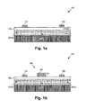
- Figure 1 a shows a cross-sectional view corresponding to an initial structure, illustrated as structure 100, used in forming the exemplary III-nitride heterojunction device in Figure 1b .
- Structure 100 includes Substrate 102, III -nitride material 104, and III-nitride material 106.
- III-nitride material 104 can comprise, for example, undoped GaN and III-nitride material 106, can comprise, for example, undoped AlGaN to form a high electron mobility transistor (HEMT).
- HEMT high electron mobility transistor
- the III-nitride materials can be doped, for example, III-nitride material 104 can comprise P-type GaN to form an N-channel GaN field effect transistor (FET).
- FET N-channel GaN field effect transistor
- Substrate 102 can comprise an insulating substrate, but can be highly resistive, and can comprise materials such as silicon carbide, silicon, sapphire, and other suitable substrate materials.
- III-nitride material 104 is disposed over Substrate 102 and III-nitride material 106 is disposed on III-nitride material 104 forming a III-nitride heterojunction.
- III-nitride material 104 has a different in-plane lattice constant than III-nitride material 106 such that a conductive channel with 2DEG can form at the interface of III-nitride material 104 and III-nitride material 106.
- contacts 108 and 110 are formed on III-nitride material 106 and can comprise, for example, ohmic contacts.
- structure 100 can be configured such that current can flow between contacts 108 and 110 in the conductive channel with 2DEG.
- contacts 108 and 110 can comprise connections for source and drain terminals in the resulting III-nitride heterojunction device.
- Figure 1b shows a cross-sectional view of an exemplary III-nitride heterojunction device in accordance with one embodiment of the present invention illustrated as III-nitride heterojunction device 150.
- a device according to the present invention includes a modification to alter formation of 2DEG thereby programming the threshold voltage of the III-nitride heterojunction device.
- the modification can alter the density of 2DEG, whereby the device can be rendered nominally OFF, i.e. the 2DEG is interrupted.
- FIG. 1b shows modification 160, which alters formation of 2DEG in III-nitride heterojunction device 150.
- modification 160 comprises a negatively charged gate contact insulator 112, which includes aluminum, disposed under gate contact 140.
- Contact insulator 112 includes aluminum to generate negative charges to alter or interrupt formation of 2DEG in III-nitride heterojunction device 150.
- the negative electrical charge in gate contact insulator 112 can interact with electrons in the 2DEG to alter formation of 2DEG.
- contact insulator 112 includes aluminum introduced by doping, implanting, or other means, such as concurrent growth of aluminum as part of formation of the gate contact insulator, to negatively charge the contact insulator for interrupting the 2DEG thereunder, thereby interrupting the current carrying channel in III-nitride heterojunction device 150.
- III-nitride heterojunction device 150 does not conduct current between contacts 108 and 110 because the current carrying channel with 2DEG is interrupted underneath gate contact 140.
- Contact 140 can comprise, for example, a conductive gate contact and contact insulator 112 can comprise a gate insulator.
- III-nitride heterojunction device 150 can be operable to carry current between contacts 108 and 110 by applying electric potential to contact 140 to reestablish interrupted 2DEG and to provide a current carrying channel between contacts 108 and 110. As such, III-nitride heterojunction device 150 can operate as an enhancement mode, or normally OFF device.
- contact insulator 112 can be formed by providing an insulator and doping or implanting the insulator with aluminum to provide negative charge in contact insulator 112.
- a Silicon Nitride (SiN) insulator can be diffused with or implanted with aluminum to provide negative charges in contact insulator 112.
- contact insulator 112 can comprise a composition of Al x Si y N z (also referred to herein as "AlSiW).
- contact insulator 112 can comprise a compound concurrently grown with aluminum to provide negative charges in therein.
- an AlSiN compound can be formed over III-nitride material 106.
- contact insulator 112 can include aluminum to program the threshold voltage of III-nitride heterojunction device 150.
- the negative charge in contact insulator 112 can be adjusted by altering the composition of contact insulator 112.
- increasing negative charge in contact insulator 112 can increase its repulsive force to alter 2DEG.
- increasing the negative charge in contact insulator 112 can increase threshold voltage such that increased electric potential must be applied to contact 140 to reestablish interrupted 2DEG and to provide a current carrying channel between contacts 108.
- selecting the composition of contact insulator 112 can program or set the threshold voltage of III-nitride heterojunction device 150.
- structure 100 in Figure 1a does not limit the formation of III-nitride heterojunction device 150.
- contacts 108 and 110 can be formed subsequent to modification 160.
- III-nitride heterojunction device 150 comprises an enhancement mode, or normally OFF device, in other embodiments contact insulator 112 can alter 2DEG formation to program or set threshold voltage in depletion mode devices.
- modification 160 as described above includes a contact insulator under a contact and over one of the III-nitride materials
- additional elements can cooperate to alter formation of 2DEG.
- Other embodiments can comprise, for example, a recess, an ion implanted region, a diffused region, an oxidation region, and/or a nitridation region.
- the additional elements can be combined in a III-nitride heterojunction device. It will be appreciated that the additional elements can be formed in additional materials or structures.
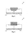
- Figure 2 shows a cross-sectional view of a portion of a III-nitride heterojunction device including an exemplary modification illustrated as modification 260.
- Modification 260 can correspond to modification 160 in Figure 1b .
- III-nitride material 204, III-nitride material 206, contact insulator 212, and contact 240 which can correspond to nitride material 104, III-nitride material 106, contact insulator 112, and contact 140 in Figure 1b .
- modification 260 includes contact insulator 212 formed over recess 230.
- Recess 230 is formed in III-nitride material 206 under contact 240 and can alter formation of 2DEG under gate contact 240.
- recess 230 permits contact 240 and contact insulator 212 to be disposed closer to the 2DEG and the interface of III-nitride material 206 and III-nitride material 204.
- recess 230 and contact insulator 212 cooperate to alter formation of 2DEG.
- contact insulator 212 can require less charge to program threshold voltage and interrupt 2DEG formation relative to contact insulator 112 in Figure 1b .
- Recess 230 can be formed, for example, by disposing photoresist over III-nitride material 206 and forming openings with sloped sidewalls in the photoresist to permit an etching step to transfer sloped geometry to III-nitride material 206. While recess 230 includes sloping sidewalls, in will be appreciated that recess 230 can comprise other geometries.
- Modification 360 can correspond to modification 160 in Figure 1b .
- modification 360 includes contact insulator 312 formed over region 370.
- Region 370 is formed in III-nitride material 306 under contact 340 and can alter formation of 2DEG under gate contact 340.
- region 370 and contact insulator 312 cooperate to alter formation of 2DEG.
- region 370 can comprise an implanted region including lattice damage, which can disrupt the bond structure and 2DEG thereunder.
- region 370 can comprise a region oxidized, nitridized, or diffused with dopants.
- modification 360 can comprise additional elements, such as a recess similar to recess 230 and/or multiple regions similar to region 370. While in Figure 3 region 370 is formed in III-nitride material 306, in other embodiments region 370 can be formed in III-nitride material 304 or in other materials. Furthermore, in some embodiments region 370 can overlap materials, for example, III-nitride materials 306 and 304. Thus, in modification 360, contact insulator 312 can require less charge to program threshold voltage and interrupt 2DEG formation relative to contact insulator 112 in Figure 1b .
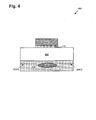
- FIG. 4 a cross-sectional view of a portion of a III-nitride heterojunction device including an exemplary modification illustrated as modification 460 is shown.
- III-nitride material 404, III-nitride material 406, contact insulator 412, and contact 440 which can correspond to nitride material 104, III-nitride material 106, contact insulator 112, and contact 140 in Figure 1b .
- modification 460 includes contact insulator 412 formed over region 480.
- Region 480 is formed in III-nitride material 404 under contact 340 and can alter formation of 2DEG under gate contact 340.
- region 480 can be formed in III-nitride material 406 or overlapping III-nitride materials 404 and 406.
- region 480 and contact insulator 412 cooperate to alter formation of 2DEG.
- contact insulator 412 can require less charge to program threshold voltage and interrupt 2DEG formation relative to contact insulator 112 in Figure 1b .
- Region 480 can comprise, for example, a region doped with p type dopants. Standard implantation and annealing steps can be used to form region 480 through III-nitride material 406. In some embodiments region 480 can be formed in III-nitride material 404, and subsequently covered by a layer of GaN, followed by AlGaN. P type dopants used for forming region 480 can comprise, for example, Fl, Mg, Fe, Cr, or Zn although other dopants can be used.
- a modification is provided to alter formation of 2DEG in the conduction channel of a III-nitride heterojunction device.
- the modification can program the threshold voltage of the device and can alter formation of 2DEG in the conduction channel to interrupt the 2DEG to obtain a nominally OFF device, rather than a nominally ON device.
- the present invention can provide for enhancement mode III-nitride heterojunction devices that can, for example, be used in power applications without being compensated during start-up to avoid conducting current while control circuitry is powering up.
- the invention provides for programming, i.e. adjusting, the threshold voltage of a resulting enhancement mode device (or even programming the threshold voltage of a depletion mode device).
Landscapes
- Junction Field-Effect Transistors (AREA)
- Insulated Gate Type Field-Effect Transistor (AREA)
- Thin Film Transistor (AREA)
Abstract
Description
- The present application claims the benefit of and priority to a pending provisional application entitled "Programmable III-Nitride Transistor with Aluminum-Doped Gate," Serial Number
61/340,802 filed on March 22, 2010 - In the present application, "group III-V semiconductor" or the like refers to a compound semiconductor that includes at least one group III element and at least one group V element, such as, but not limited to, gallium nitride (GaN), gallium arsenide (GaAs), aluminum gallium arsenide (AlGaAs), indium gallium nitride (InGaN) and the like. Analogously, "III-nitride semiconductor" or the like refers to a compound semiconductor that includes nitrogen and at least one group III element, such as, but not limited to, GaN, AlGaN, InN, AlN, InGaN, InAlGaN and the like.
- The present invention relates generally to semiconductors, and more particularly to transistors and devices based on III-nitride semiconductors.
- Devices based on III-nitride heterojunction structures typically operate using piezoelectric polarization fields to generate a two dimensional electron gas (2DEG) that allows for high current densities with low resistive losses. The 2DEG is formed by an interface of III-nitride materials and, due to the 2DEG, conventional III-nitride heterojunction devices may conduct without the application of a gate potential. Thus, devices that are formed using III-nitride heterojunction structures tend to be nominally ON, or depletion mode devices.
- III-nitride heterojunction devices are desirable for power applications due to relatively high breakdown voltage, high current density, and low "on resistance." However, the nominally ON nature of conventional 111-nitride heterojunction devices can introduce problems when used in power applications. For example, in power applications it is desirable to avoid conducting current through III-nitride heterojunction devices before control circuitry is fully powered and operational. Accordingly, it would be desirable to provide 111-nitride heterojunction devices that are nominally OFF, or enhancement mode to, for example, avoid current conduction problems during start-up and other modes.
- The present application is directed to a programmable III-nitride transistor with aluminum-doped gate, substantially as shown in and/or described in connection with at least one of the figures, as set forth more completely in the claims.
-
-
Figure 1 a illustrates a cross-sectional view corresponding to an initial structure used in forming the exemplary III-nitride heterojunction device inFigure 1b . -
Figure 1b illustrates a cross-sectional view of an exemplary III-nitride heterojunction device in accordance with one embodiment of the present invention. -
Figure 2 illustrates a cross-sectional view of a portion of a III-nitride heterojunction device including an exemplary modification in accordance with one embodiment of the present invention. -
Figure 3 illustrates a cross-sectional view of a portion of a III-nitride heterojunction device including an exemplary modification in accordance with one embodiment of the present invention. -
Figure 4 illustrates a cross-sectional view of a portion of a III-nitride heterojunction device including an exemplary modification in accordance with one embodiment of the present invention. - The present invention is directed to III-nitride devices, particularly enhancement mode III-nitride devices, including modification to alter formation of 2DEG (two dimensional electron gas). Modifications based on aluminum introduction, for example by doping or other methods, are of notable interest in the present invention. The following description contains specific information pertaining to the implementation of the present invention. One skilled in the art will recognize that the present invention may be implemented in a manner different from that specifically discussed in the present application. Moreover, some of the specific details of the invention are not discussed in order not to obscure the invention.
- The drawings in the present application and their accompanying detailed description are directed to merely exemplary embodiments of the invention. To maintain brevity, other embodiments of the present invention are not specifically described in the present application and are not specifically illustrated by the present drawings. While GaN and AlGaN materials are specifically referred to in this application, different materials can be used such that an interface between the materials can form a conductive channel including 2DEG. Furthermore, while two III-nitride materials and layers are described, it will be appreciated that additional materials and layers can be included without departing from the scope of the present invention.
-
Figure 1 a shows a cross-sectional view corresponding to an initial structure, illustrated asstructure 100, used in forming the exemplary III-nitride heterojunction device inFigure 1b .Structure 100 includesSubstrate 102, III -nitride material 104, and III-nitride material 106. In some embodiments, III-nitride material 104 can comprise, for example, undoped GaN and III-nitride material 106, can comprise, for example, undoped AlGaN to form a high electron mobility transistor (HEMT). In other embodiments the III-nitride materials can be doped, for example, III-nitride material 104 can comprise P-type GaN to form an N-channel GaN field effect transistor (FET). -
Substrate 102 can comprise an insulating substrate, but can be highly resistive, and can comprise materials such as silicon carbide, silicon, sapphire, and other suitable substrate materials. InFigure 1a , III-nitride material 104 is disposed overSubstrate 102 and III-nitride material 106 is disposed on III-nitride material 104 forming a III-nitride heterojunction. III-nitride material 104 has a different in-plane lattice constant than III-nitride material 106 such that a conductive channel with 2DEG can form at the interface of III-nitride material 104 and III-nitride material 106. - Also shown in
Figure 1a ,contacts nitride material 106 and can comprise, for example, ohmic contacts. Thus,structure 100 can be configured such that current can flow betweencontacts contacts -
Figure 1b shows a cross-sectional view of an exemplary III-nitride heterojunction device in accordance with one embodiment of the present invention illustrated as III-nitride heterojunction device 150. A device according to the present invention includes a modification to alter formation of 2DEG thereby programming the threshold voltage of the III-nitride heterojunction device. In particular embodiments, the modification can alter the density of 2DEG, whereby the device can be rendered nominally OFF, i.e. the 2DEG is interrupted. -
Figure 1b showsmodification 160, which alters formation of 2DEG in III-nitride heterojunction device 150. In III-nitride heterojunction device 150,modification 160 comprises a negatively chargedgate contact insulator 112, which includes aluminum, disposed undergate contact 140.Contact insulator 112 includes aluminum to generate negative charges to alter or interrupt formation of 2DEG in III-nitride heterojunction device 150. Thus, the negative electrical charge ingate contact insulator 112 can interact with electrons in the 2DEG to alter formation of 2DEG. - In the embodiment shown in
Figure 1b ,contact insulator 112 includes aluminum introduced by doping, implanting, or other means, such as concurrent growth of aluminum as part of formation of the gate contact insulator, to negatively charge the contact insulator for interrupting the 2DEG thereunder, thereby interrupting the current carrying channel in III-nitride heterojunction device 150. In an inactive state, III-nitride heterojunction device 150 does not conduct current betweencontacts gate contact 140. Contact 140 can comprise, for example, a conductive gate contact andcontact insulator 112 can comprise a gate insulator. Thus, III-nitride heterojunction device 150 can be operable to carry current betweencontacts contacts nitride heterojunction device 150 can operate as an enhancement mode, or normally OFF device. - In some embodiments,
contact insulator 112 can be formed by providing an insulator and doping or implanting the insulator with aluminum to provide negative charge incontact insulator 112. For example, a Silicon Nitride (SiN) insulator can be diffused with or implanted with aluminum to provide negative charges incontact insulator 112. In particularembodiments contact insulator 112 can comprise a composition of AlxSiyNz (also referred to herein as "AlSiW). In otherembodiments contact insulator 112 can comprise a compound concurrently grown with aluminum to provide negative charges in therein. For example, an AlSiN compound can be formed over III-nitride material 106. - Also in III-
nitride heterojunction device 150,contact insulator 112 can include aluminum to program the threshold voltage of III-nitride heterojunction device 150. For example, the negative charge incontact insulator 112 can be adjusted by altering the composition ofcontact insulator 112. For example, in III-nitride heterojunction device 150, increasing negative charge incontact insulator 112 can increase its repulsive force to alter 2DEG. As such, increasing the negative charge incontact insulator 112 can increase threshold voltage such that increased electric potential must be applied to contact 140 to reestablish interrupted 2DEG and to provide a current carrying channel betweencontacts 108. Thus, selecting the composition ofcontact insulator 112 can program or set the threshold voltage of III-nitride heterojunction device 150. - It will be appreciated that
structure 100 inFigure 1a does not limit the formation of III-nitride heterojunction device 150. For example, in some embodiments,contacts modification 160. Also, while III-nitride heterojunction device 150 comprises an enhancement mode, or normally OFF device, in other embodiments contactinsulator 112 can alter 2DEG formation to program or set threshold voltage in depletion mode devices. - Furthermore, while
modification 160 as described above includes a contact insulator under a contact and over one of the III-nitride materials, in other embodiments, additional elements can cooperate to alter formation of 2DEG. Other embodiments can comprise, for example, a recess, an ion implanted region, a diffused region, an oxidation region, and/or a nitridation region. Furthermore, the additional elements can be combined in a III-nitride heterojunction device. It will be appreciated that the additional elements can be formed in additional materials or structures. - Referring now to
Figure 2, Figure 2 shows a cross-sectional view of a portion of a III-nitride heterojunction device including an exemplary modification illustrated asmodification 260.Modification 260 can correspond tomodification 160 inFigure 1b . InFigure 2 , III-nitride material 204, III-nitride material 206,contact insulator 212, and contact 240, which can correspond tonitride material 104, III-nitride material 106,contact insulator 112, and contact 140 inFigure 1b . - As shown in
Figure 2 ,modification 260 includescontact insulator 212 formed overrecess 230.Recess 230 is formed in III-nitride material 206 under contact 240 and can alter formation of 2DEG under gate contact 240. Furthermore, recess 230 permits contact 240 andcontact insulator 212 to be disposed closer to the 2DEG and the interface of III-nitride material 206 and III-nitride material 204. Inmodification 260,recess 230 andcontact insulator 212 cooperate to alter formation of 2DEG. Thus, inmodification 260,contact insulator 212 can require less charge to program threshold voltage and interrupt 2DEG formation relative to contactinsulator 112 inFigure 1b . - Recess 230 can be formed, for example, by disposing photoresist over III-
nitride material 206 and forming openings with sloped sidewalls in the photoresist to permit an etching step to transfer sloped geometry to III-nitride material 206. Whilerecess 230 includes sloping sidewalls, in will be appreciated thatrecess 230 can comprise other geometries. - Referring now to
Figure 3 , a cross-sectional view of a portion of a III-nitride heterojunction device including an exemplary modification illustrated asmodification 360 is shown.Modification 360 can correspond tomodification 160 inFigure 1b . InFigure 3 , III-nitride material 304, III-nitride material 306,contact insulator 312, and contact 340, which can correspond tonitride material 104, III-nitride material 106,contact insulator 112, and contact 140 inFigure 1b . - As shown in
Figure 3 ,modification 360 includescontact insulator 312 formed overregion 370.Region 370 is formed in III-nitride material 306 under contact 340 and can alter formation of 2DEG under gate contact 340. Inmodification 360,region 370 andcontact insulator 312 cooperate to alter formation of 2DEG. - In some
embodiments region 370 can comprise an implanted region including lattice damage, which can disrupt the bond structure and 2DEG thereunder. In other embodiments,region 370 can comprise a region oxidized, nitridized, or diffused with dopants. Also, as described above,modification 360 can comprise additional elements, such as a recess similar torecess 230 and/or multiple regions similar toregion 370. While inFigure 3 region 370 is formed in III-nitride material 306, inother embodiments region 370 can be formed in III-nitride material 304 or in other materials. Furthermore, in someembodiments region 370 can overlap materials, for example, III-nitride materials modification 360,contact insulator 312 can require less charge to program threshold voltage and interrupt 2DEG formation relative to contactinsulator 112 inFigure 1b . - Referring now to
Figure 4 , a cross-sectional view of a portion of a III-nitride heterojunction device including an exemplary modification illustrated asmodification 460 is shown. InFigure 4 , III-nitride material 404, III-nitride material 406,contact insulator 412, and contact 440, which can correspond tonitride material 104, III-nitride material 106,contact insulator 112, and contact 140 inFigure 1b . - As shown in
Figure 4 ,modification 460 includescontact insulator 412 formed overregion 480.Region 480 is formed in III-nitride material 404 under contact 340 and can alter formation of 2DEG under gate contact 340. Inother embodiments region 480 can be formed in III-nitride material 406 or overlapping III-nitride materials modification 460,region 480 andcontact insulator 412 cooperate to alter formation of 2DEG. Thus, inmodification 460,contact insulator 412 can require less charge to program threshold voltage and interrupt 2DEG formation relative to contactinsulator 112 inFigure 1b . -
Region 480 can comprise, for example, a region doped with p type dopants. Standard implantation and annealing steps can be used to formregion 480 through III-nitride material 406. In someembodiments region 480 can be formed in III-nitride material 404, and subsequently covered by a layer of GaN, followed by AlGaN. P type dopants used for formingregion 480 can comprise, for example, Fl, Mg, Fe, Cr, or Zn although other dopants can be used. - In the embodiments in
Figures 1b and2 through4 , a modification is provided to alter formation of 2DEG in the conduction channel of a III-nitride heterojunction device. The modification can program the threshold voltage of the device and can alter formation of 2DEG in the conduction channel to interrupt the 2DEG to obtain a nominally OFF device, rather than a nominally ON device. Accordingly, the present invention can provide for enhancement mode III-nitride heterojunction devices that can, for example, be used in power applications without being compensated during start-up to avoid conducting current while control circuitry is powering up. Moreover, the invention provides for programming, i.e. adjusting, the threshold voltage of a resulting enhancement mode device (or even programming the threshold voltage of a depletion mode device). - From the above description of the invention it is manifest that various techniques can be used for implementing the concepts of the present invention without departing from its scope. Moreover, while the invention has been described with specific reference to certain embodiments, a person of ordinary skill in the art would appreciate that changes can be made in form and detail without departing from the spirit and the scope of the invention. Thus, the described embodiments are to be considered in all respects as illustrative and not restrictive. It should also be understood that the invention is not limited to the particular embodiments described herein but is capable of many rearrangements, modifications, and substitutions without departing from the scope of the invention.
Claims (15)
- A III-nitride heterojunction device comprising:a conduction channel including a two dimensional electron gas formed at an interface between a first III-nitride material and a second III-nitride material;a modification including a contact insulator disposed over said conduction channel, said contact insulator including aluminum to alter formation of said two dimensional electron gas at said interface.
- The III-nitride heterojunction device of claim 1, wherein said contact insulator comprises AlSiN.
- The III-nitride heterojunction device of claim 2, wherein said contact insulator is grown as a compound.
- The III-nitride heterojunction device of claim 1, wherein said contact insulator comprises SiN doped with aluminum.
- The III-nitride heterojunction device of claim 1, wherein said modification programs a threshold voltage of said III-nitride heterojunction device.
- The III-nitride heterojunction device of claim 1, wherein said modification alters formation of said two dimensional electron gas to interrupt said conduction channel.
- The III-nitride heterojunction device of claim 1, wherein said modification further includes a recess.
- The III-nitride heterojunction device of claim 1, wherein said modification further includes an ion implanted region.
- The III-nitride heterojunction device of claim 1, wherein said modification further includes a diffused region.
- The III-nitride heterojunction device of claim 1, wherein said modification further includes an oxidation region.
- The III-nitride heterojunction device of claim 1, wherein said modification further includes a nitridation region.
- The III-nitride heterojunction device of claim 1, wherein said contact insulator is a gate insulator formed under a gate contact.
- The III-nitride heterojunction device of claim 1, wherein said first III-nitride material comprises GaN and said second III-nitride material comprises AlGaN.
- The III-nitride heterojunction device of claim 1, wherein said III-nitride heterojunction device is an N-channel GaN FET.
- An enhancement mode III-nitride heterojunction device comprising:a conduction channel including a two dimensional electron gas formed at an interface between a first III-nitride material and a second III-nitride material;a modification interrupting said conduction channel, said modification including a gate insulator disposed over said conduction channel, said gate insulator including aluminum to alter formation of said two dimensional electron gas at said interface.
Applications Claiming Priority (2)
| Application Number | Priority Date | Filing Date | Title |
|---|---|---|---|
| US34080210P | 2010-03-22 | 2010-03-22 | |
| US13/021,437 US9105703B2 (en) | 2010-03-22 | 2011-02-04 | Programmable III-nitride transistor with aluminum-doped gate |
Publications (2)
| Publication Number | Publication Date |
|---|---|
| EP2369628A2 true EP2369628A2 (en) | 2011-09-28 |
| EP2369628A3 EP2369628A3 (en) | 2013-05-08 |
Family
ID=44168929
Family Applications (1)
| Application Number | Title | Priority Date | Filing Date |
|---|---|---|---|
| EP11001844.7A Withdrawn EP2369628A3 (en) | 2010-03-22 | 2011-03-05 | Programmable III-nitride transistor with aluminum-doped gate |
Country Status (3)
| Country | Link |
|---|---|
| US (1) | US9105703B2 (en) |
| EP (1) | EP2369628A3 (en) |
| JP (1) | JP5979819B2 (en) |
Cited By (1)
| Publication number | Priority date | Publication date | Assignee | Title |
|---|---|---|---|---|
| CN105849911A (en) * | 2013-10-11 | 2016-08-10 | 国家科学研究中心 | HEMT made from a heterojunction |
Families Citing this family (19)
| Publication number | Priority date | Publication date | Assignee | Title |
|---|---|---|---|---|
| US9219058B2 (en) * | 2010-03-01 | 2015-12-22 | Infineon Technologies Americas Corp. | Efficient high voltage switching circuits and monolithic integration of same |
| US8981380B2 (en) * | 2010-03-01 | 2015-03-17 | International Rectifier Corporation | Monolithic integration of silicon and group III-V devices |
| US8957454B2 (en) | 2011-03-03 | 2015-02-17 | International Rectifier Corporation | III-Nitride semiconductor structures with strain absorbing interlayer transition modules |
| US8546849B2 (en) | 2011-05-04 | 2013-10-01 | International Rectifier Corporation | High voltage cascoded III-nitride rectifier package utilizing clips on package surface |
| US8796738B2 (en) | 2011-09-21 | 2014-08-05 | International Rectifier Corporation | Group III-V device structure having a selectively reduced impurity concentration |
| JP5895651B2 (en) * | 2012-03-28 | 2016-03-30 | 富士通株式会社 | Compound semiconductor device and manufacturing method thereof |
| JP6054620B2 (en) * | 2012-03-29 | 2016-12-27 | トランスフォーム・ジャパン株式会社 | Compound semiconductor device and manufacturing method thereof |
| JP6161887B2 (en) * | 2012-09-28 | 2017-07-12 | トランスフォーム・ジャパン株式会社 | Compound semiconductor device and manufacturing method thereof |
| US8928037B2 (en) * | 2013-02-28 | 2015-01-06 | Power Integrations, Inc. | Heterostructure power transistor with AlSiN passivation layer |
| US9111956B2 (en) | 2013-03-14 | 2015-08-18 | Taiwan Semiconductor Manufacturing Company, Ltd. | Rectifier structures with low leakage |
| US9202906B2 (en) | 2013-03-14 | 2015-12-01 | Northrop Grumman Systems Corporation | Superlattice crenelated gate field effect transistor |
| JP6171435B2 (en) * | 2013-03-18 | 2017-08-02 | 富士通株式会社 | Semiconductor device and manufacturing method thereof, power supply device, and high-frequency amplifier |
| JP2016004948A (en) * | 2014-06-18 | 2016-01-12 | 株式会社東芝 | Semiconductor device |
| US10923584B2 (en) | 2016-07-01 | 2021-02-16 | Intel Corporation | Graded channels for high frequency III-N transistors |
| JP7203727B2 (en) | 2017-07-07 | 2023-01-13 | パナソニックホールディングス株式会社 | semiconductor equipment |
| CN109659361B (en) | 2017-10-12 | 2022-03-04 | 电力集成公司 | Gate stack for heterojunction devices |
| CN212062440U (en) * | 2020-06-24 | 2020-12-01 | 广东致能科技有限公司 | Normally-off device |
| WO2024065310A1 (en) * | 2022-09-28 | 2024-04-04 | Innoscience (suzhou) Semiconductor Co., Ltd. | Nitride-based semiconductor device and method for manufacturing thereof |
| US12107585B2 (en) | 2022-09-29 | 2024-10-01 | Globalfoundries U.S. Inc. | Comparator circuits |
Citations (1)
| Publication number | Priority date | Publication date | Assignee | Title |
|---|---|---|---|---|
| US20090146185A1 (en) * | 2007-12-10 | 2009-06-11 | Transphorm Inc. | Insulated gate e-mode transistors |
Family Cites Families (9)
| Publication number | Priority date | Publication date | Assignee | Title |
|---|---|---|---|---|
| EP1410444B1 (en) | 2001-07-24 | 2012-08-22 | Cree, Inc. | Insulating Gate AlGaN/GaN HEMT |
| US7382001B2 (en) | 2004-01-23 | 2008-06-03 | International Rectifier Corporation | Enhancement mode III-nitride FET |
| JP5192683B2 (en) * | 2006-11-17 | 2013-05-08 | 古河電気工業株式会社 | Nitride-based semiconductor heterojunction field effect transistor |
| US8062931B2 (en) * | 2006-11-21 | 2011-11-22 | Imec | Surface treatment and passivation of AlGaN/GaN HEMT |
| US8455920B2 (en) | 2007-05-23 | 2013-06-04 | International Rectifier Corporation | III-nitride heterojunction device |
| WO2009038809A1 (en) | 2007-09-20 | 2009-03-26 | International Rectifier Corporation | Enhancement mode iii-nitride semiconductor device with reduced electric field between the gate and the drain |
| US8519438B2 (en) | 2008-04-23 | 2013-08-27 | Transphorm Inc. | Enhancement mode III-N HEMTs |
| JP5337415B2 (en) * | 2008-06-30 | 2013-11-06 | シャープ株式会社 | Heterojunction field effect transistor and method of manufacturing heterojunction field effect transistor |
| US7985986B2 (en) * | 2008-07-31 | 2011-07-26 | Cree, Inc. | Normally-off semiconductor devices |
-
2011
- 2011-02-04 US US13/021,437 patent/US9105703B2/en active Active
- 2011-03-05 EP EP11001844.7A patent/EP2369628A3/en not_active Withdrawn
- 2011-03-15 JP JP2011056226A patent/JP5979819B2/en active Active
Patent Citations (1)
| Publication number | Priority date | Publication date | Assignee | Title |
|---|---|---|---|---|
| US20090146185A1 (en) * | 2007-12-10 | 2009-06-11 | Transphorm Inc. | Insulated gate e-mode transistors |
Cited By (1)
| Publication number | Priority date | Publication date | Assignee | Title |
|---|---|---|---|---|
| CN105849911A (en) * | 2013-10-11 | 2016-08-10 | 国家科学研究中心 | HEMT made from a heterojunction |
Also Published As
| Publication number | Publication date |
|---|---|
| EP2369628A3 (en) | 2013-05-08 |
| US20110227090A1 (en) | 2011-09-22 |
| JP2011199286A (en) | 2011-10-06 |
| US9105703B2 (en) | 2015-08-11 |
| JP5979819B2 (en) | 2016-08-31 |
Similar Documents
| Publication | Publication Date | Title |
|---|---|---|
| US9105703B2 (en) | Programmable III-nitride transistor with aluminum-doped gate | |
| JP5044222B2 (en) | Group III nitride current control device and manufacturing method | |
| CN101273458B (en) | Enhancement Mode Group III Nitride Field Effect Transistor | |
| US9837518B2 (en) | Semiconductor device | |
| US8633518B2 (en) | Gallium nitride power devices | |
| US9196614B2 (en) | Inverted III-nitride P-channel field effect transistor with hole carriers in the channel | |
| US9437708B2 (en) | Enhancement mode III-N HEMTs | |
| US8878246B2 (en) | High electron mobility transistors and methods of fabricating the same | |
| US20080308813A1 (en) | High breakdown enhancement mode gallium nitride based high electron mobility transistors with integrated slant field plate | |
| JP2020053585A (en) | Nitride semiconductor device and method of manufacturing the same | |
| KR20140057543A (en) | Method for growing iii-v epitaxial layers and semiconductor structure | |
| WO2010151721A1 (en) | Transistor with enhanced channel charge inducing material layer and threshold voltage control | |
| KR20200045141A (en) | IMPLANTING METHOD FOR GaN SEMICONDUCTOR PROCESSING |
Legal Events
| Date | Code | Title | Description |
|---|---|---|---|
| PUAI | Public reference made under article 153(3) epc to a published international application that has entered the european phase |
Free format text: ORIGINAL CODE: 0009012 |
|
| AK | Designated contracting states |
Kind code of ref document: A2 Designated state(s): AL AT BE BG CH CY CZ DE DK EE ES FI FR GB GR HR HU IE IS IT LI LT LU LV MC MK MT NL NO PL PT RO RS SE SI SK SM TR |
|
| AX | Request for extension of the european patent |
Extension state: BA ME |
|
| PUAL | Search report despatched |
Free format text: ORIGINAL CODE: 0009013 |
|
| AK | Designated contracting states |
Kind code of ref document: A3 Designated state(s): AL AT BE BG CH CY CZ DE DK EE ES FI FR GB GR HR HU IE IS IT LI LT LU LV MC MK MT NL NO PL PT RO RS SE SI SK SM TR |
|
| AX | Request for extension of the european patent |
Extension state: BA ME |
|
| RIC1 | Information provided on ipc code assigned before grant |
Ipc: H01L 29/778 20060101AFI20130403BHEP Ipc: H01L 29/423 20060101ALI20130403BHEP Ipc: H01L 29/207 20060101ALI20130403BHEP Ipc: H01L 29/20 20060101ALI20130403BHEP Ipc: H01L 29/80 20060101ALI20130403BHEP |
|
| 17P | Request for examination filed |
Effective date: 20131105 |
|
| RBV | Designated contracting states (corrected) |
Designated state(s): AL AT BE BG CH CY CZ DE DK EE ES FI FR GB GR HR HU IE IS IT LI LT LU LV MC MK MT NL NO PL PT RO RS SE SI SK SM TR |
|
| 17Q | First examination report despatched |
Effective date: 20151014 |
|
| RAP1 | Party data changed (applicant data changed or rights of an application transferred) |
Owner name: INFINEON TECHNOLOGIES AMERICAS CORP. |
|
| STAA | Information on the status of an ep patent application or granted ep patent |
Free format text: STATUS: THE APPLICATION IS DEEMED TO BE WITHDRAWN |
|
| 18D | Application deemed to be withdrawn |
Effective date: 20200603 |