EP2368166B1 - Strom-management - Google Patents
Strom-management Download PDFInfo
- Publication number
- EP2368166B1 EP2368166B1 EP09796657.6A EP09796657A EP2368166B1 EP 2368166 B1 EP2368166 B1 EP 2368166B1 EP 09796657 A EP09796657 A EP 09796657A EP 2368166 B1 EP2368166 B1 EP 2368166B1
- Authority
- EP
- European Patent Office
- Prior art keywords
- circuitry
- power state
- memory
- secure transaction
- transaction
- Prior art date
- Legal status (The legal status is an assumption and is not a legal conclusion. Google has not performed a legal analysis and makes no representation as to the accuracy of the status listed.)
- Not-in-force
Links
Images



Classifications
-
- G—PHYSICS
- G06—COMPUTING OR CALCULATING; COUNTING
- G06F—ELECTRIC DIGITAL DATA PROCESSING
- G06F1/00—Details not covered by groups G06F3/00 - G06F13/00 and G06F21/00
- G06F1/26—Power supply means, e.g. regulation thereof
- G06F1/32—Means for saving power
- G06F1/3203—Power management, i.e. event-based initiation of a power-saving mode
- G06F1/3234—Power saving characterised by the action undertaken
- G06F1/3287—Power saving characterised by the action undertaken by switching off individual functional units in the computer system
-
- G—PHYSICS
- G06—COMPUTING OR CALCULATING; COUNTING
- G06F—ELECTRIC DIGITAL DATA PROCESSING
- G06F1/00—Details not covered by groups G06F3/00 - G06F13/00 and G06F21/00
- G06F1/26—Power supply means, e.g. regulation thereof
- G06F1/32—Means for saving power
- G06F1/3203—Power management, i.e. event-based initiation of a power-saving mode
- G06F1/3206—Monitoring of events, devices or parameters that trigger a change in power modality
- G06F1/3209—Monitoring remote activity, e.g. over telephone lines or network connections
-
- G—PHYSICS
- G06—COMPUTING OR CALCULATING; COUNTING
- G06K—GRAPHICAL DATA READING; PRESENTATION OF DATA; RECORD CARRIERS; HANDLING RECORD CARRIERS
- G06K19/00—Record carriers for use with machines and with at least a part designed to carry digital markings
- G06K19/06—Record carriers for use with machines and with at least a part designed to carry digital markings characterised by the kind of the digital marking, e.g. shape, nature, code
- G06K19/067—Record carriers with conductive marks, printed circuits or semiconductor circuit elements, e.g. credit or identity cards also with resonating or responding marks without active components
- G06K19/07—Record carriers with conductive marks, printed circuits or semiconductor circuit elements, e.g. credit or identity cards also with resonating or responding marks without active components with integrated circuit chips
- G06K19/0701—Record carriers with conductive marks, printed circuits or semiconductor circuit elements, e.g. credit or identity cards also with resonating or responding marks without active components with integrated circuit chips at least one of the integrated circuit chips comprising an arrangement for power management
-
- Y—GENERAL TAGGING OF NEW TECHNOLOGICAL DEVELOPMENTS; GENERAL TAGGING OF CROSS-SECTIONAL TECHNOLOGIES SPANNING OVER SEVERAL SECTIONS OF THE IPC; TECHNICAL SUBJECTS COVERED BY FORMER USPC CROSS-REFERENCE ART COLLECTIONS [XRACs] AND DIGESTS
- Y02—TECHNOLOGIES OR APPLICATIONS FOR MITIGATION OR ADAPTATION AGAINST CLIMATE CHANGE
- Y02D—CLIMATE CHANGE MITIGATION TECHNOLOGIES IN INFORMATION AND COMMUNICATION TECHNOLOGIES [ICT], I.E. INFORMATION AND COMMUNICATION TECHNOLOGIES AIMING AT THE REDUCTION OF THEIR OWN ENERGY USE
- Y02D10/00—Energy efficient computing, e.g. low power processors, power management or thermal management
Definitions
- Embodiments of the present invention relate to power management. In particular, they relate to conserving power when using a portable memory apparatus.
- An electronic device may comprise secure transaction circuitry connected to a near field communication transceiver. If a user places the near field communication transceiver near to a further near field transceiver of a further apparatus, a transaction may be conducted with the further apparatus using the secure transaction circuitry.
- WO 2006/095212 A1 discloses a mobile terminal device comprising a smart card module and a near field communication module.
- the smart card operation on the mobile terminal device When the smart card operation on the mobile terminal device is started it results in an activation or switching on of the smart card module.
- a smart card application may be started by a user or based on the location of the mobile terminal device. The latter is the case, for instance, if the mobile terminal device is located in the area of a point of sales terminal.
- the invention relates to a method, a computer program and an apapratus as defined in the appended independent claims. Further specific embodiments are defined in the dependent claims.
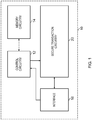
- the Figures illustrate an apparatus 10, comprising: secure transaction circuitry 20 having a first power state and a second power state, the secure transaction circuitry 20 being configured, when in the second power state, to perform a transaction, using a transceiver 16, with a further apparatus 70; memory circuitry 14 having power states; and control circuitry 12/13/22 configured to detect a first electrical signal provided by the transceiver 16 and configured, in response to detecting the first electrical signal, to control the secure transaction circuitry 20 to switch from being in the first power state to being in the second power state, without changing a power state of the memory circuitry 14.
- Fig. 1 illustrates a general schematic of an apparatus 10.
- the apparatus may be a portable memory apparatus.
- the portable memory apparatus 10 may, for example, be a hand portable memory stick/card.
- the portable memory apparatus 10 may be a Micro Secure Digital (SD) card.
- SD Micro Secure Digital
- the portable memory apparatus 10 may, for example, comprise a housing that is configured to be insertable into a receptacle of an electronic device by a user without the use of a tool and be removable from the receptacle of the electronic device by a user without the use of a tool.
- the receptacle may be a slot in the electronic device.
- the apparatus 10 illustrated in Fig. 1 comprises control circuitry 12, memory circuitry 14, an interface 18 and secure transaction circuitry 20.
- the secure transaction circuitry 20 may be "secure” because it is tamper-resistant.
- the tamper resistivity of the secure transaction circuitry 20 may be provided by the physical/mechanical properties of the secure transaction circuitry 20 or the physical/mechanical properties of a housing of the secure transaction circuitry 20. Additionally or alternatively, tamper resistivity may be provided by encryption of data and/or computer program instructions stored in secure transaction memory circuitry of the secure transaction circuitry 20.
- the apparatus 10 may, for example, comprise a housing that houses some or all of the control circuitry 12, the memory circuitry 14, the interface 18 and the secure transaction circuitry 20.
- Fig. 2 illustrates an electronic device 40.
- the electronic device 40 may be a hand portable electronic device such as a mobile telephone, a personal digital assistant or a personal music player.
- the electronic device 40 comprises a portable memory apparatus 10 in accordance with embodiments of the invention.
- the schematic of the portable memory apparatus 10 in Fig.2 is a more detailed version of that illustrated in Fig. 1 .
- the electronic device 40 comprises a processor 30 and a transceiver 16.
- the processor 30 and the transceiver 16 are not, in this example, part of the portable memory apparatus 10.
- the processor 30 may, for example, be a central processor of the electronic device 40.
- the transceiver 16 may, for example, be a wireless near field communication transceiver. Alternatively, the transceiver 16 may be a short range wireless radio transceiver that operates in accordance with a 802.11g or Bluetooth protocol.
- the portable memory apparatus 10 illustrated in Fig. 2 comprises a memory controller 13, memory circuitry 14, an interface 18, a secure transaction controller 22 and secure transaction memory circuitry 24.
- the transceiver 16 is connected to the secure transaction controller 22 by an interface 18.
- the interface 18 may, for instance, comprise a single control line, or a plurality of control lines.
- the interface 18 may be an S 2 C interface (described in the standard ECMA-373, and also known as NFC-WI) comprising a SIGOUT control line from the transceiver 16 to the secure transaction controller 22 and a SIGIN control line from the secure transaction controller 22 to the transceiver 16.
- the interface 18 may be a single wire protocol (SWP) interface.
- SWP single wire protocol
- the portable memory apparatus 10 of the example embodiment of the invention illustrated in Fig. 2 relates to the portable memory apparatus illustrated in Fig. 1 in that the control circuitry 12 illustrated in Fig. 1 can be considered to be the memory controller 13 illustrated in Fig. 2 .
- the memory controller 13 is configured to receive an input from and provide an output to the processor 30, and to write to and read from the memory circuitry 14.
- the processor 30 may, for example, write data to the memory circuitry 14 using the memory controller 13.
- the memory controller 13 may, for example, be implemented using one or more field-programmable gate arrays (FPGA), application specific integrated circuits (ASIC), or software programmable processors.
- the memory controller 13 is also configured to detect inputs provided by the transceiver 16 on the interface 18, and to provide an output to the secure transaction controller 22.
- the secure transaction controller 22 and the secure transaction memory circuitry 24 can collectively be considered to be secure transaction circuitry 20 (as illustrated in Fig. 1 ).
- the secure transaction controller 22 is configured to read from the secure transaction memory circuitry 24.
- the secure transaction controller 22 may be implemented using one or more FPGAs, ASICs, or software programmable processors.
- the secure transaction memory circuitry 24 illustrated in Fig. 2 stores transaction data 28.
- the transaction data 28 may, for example, comprise user payment details such as a user's credit card or debit card details. Although the secure transaction memory circuitry 24 is illustrated as a single component, it may be implemented as one or more separate components.
- the transaction data 28 may also comprise a password. A user may be asked to enter the password in order to confirm payment should be made using his payment details.
- the memory circuitry 14 is general purpose, non-volatile memory circuitry that may be used to store data.
- the memory circuitry 14 may, for example, be flash memory.
- the memory circuitry 14 is illustrated as a single component, it may be implemented as one or more separate components.
- the memory circuitry 14 illustrated in Fig. 2 stores computer program instructions 26.
- the computer program instructions 26 control the operation of the portable memory apparatus 10 when loaded into the memory controller 13.
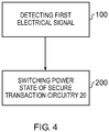
- the computer program instructions 26 provide the logic and routines that enables the portable memory apparatus 10 to perform the method illustrated in Fig 4 .
- the memory controller 13 is able, by reading the memory circuitry 14, to load and execute the computer program instructions 26.
- the computer program may arrive at the portable memory apparatus 10 via any suitable delivery mechanism 36.
- the delivery mechanism 36 may be, for example, a computer-readable storage medium, a computer program product, a memory device, a record medium such as a CD-ROM or DVD, an article of manufacture that tangibly embodies the computer program instructions 26.
- the delivery mechanism 36 may be a signal configured to reliably transfer the computer program instructions 26.
- the electronic device 40 may propagate or transmit the computer program instructions 26 as a computer data signal.
- Fig. 2 The elements illustrated in Fig. 2 are operationally coupled and any number or combination of intervening elements can exist (including no intervening elements).
- the transceiver 16 is a near field communication transceiver.
- Fig. 3 illustrates an electronic device 40, a first apparatus 60 and a second apparatus 70.
- the electronic device 40 comprises a portable memory apparatus 10.
- the first apparatus 60 comprises a near field communication transceiver 50.
- the first apparatus 60 enables a user to pay for transportation tickets (for example, train tickets).
- the first apparatus 60 is connected to a second apparatus 70.
- the second apparatus 70 may be a transaction server.
- a user places the electronic device 40 near the near field communication transceiver 50 of the first apparatus 60 in order to pay for transportation.
- the portable memory apparatus 10 Before the user places the electronic device 40 next to the apparatus 60, the portable memory apparatus 10 is inactive and in a first, standby, power state. That is, each of the memory controller 13, the memory circuitry 14 and the secure transaction circuitry 20 are in a first, standby, power state.
- the memory circuitry 14 When the memory circuitry 14 is in the standby power state, the memory circuitry 14 is unable to be written to or read from. When the memory is in an active power state, the memory circuitry 14 is able to be written to and read from. The memory circuitry 14 is not able to be in both the standby power state and the active power state at the same time. The memory circuitry 14 consumes more power when it is in the active power state than when it is in the standby power state.
- the secure transaction circuitry 20 When the secure transaction circuitry 20 is in the standby power state, the secure transaction circuitry 20 is unable to perform a transaction with an apparatus. When the secure transaction circuitry 20 is in an active power state, the secure transaction circuitry 20 is able to perform a transaction with an apparatus.
- the transaction may or may not be secure (for example, the transaction may or may not be encrypted).
- the secure transaction circuitry 20 comprises a secure transaction controller 22 and secure transaction memory circuitry 24. Neither the secure transaction controller 22 nor the secure transaction memory circuitry 24 may be in the standby power state and the active power state at the same time. The secure transaction circuitry 20 consumes more power when it is in the active power state than when it is in the standby power state.
- the apparatus 60 Upon placement of the electronic device 40 near to the apparatus 60, communication between the near field communication transceiver 16 of the electronic device 40 and the near field communication transceiver 50 of the apparatus 60 is initiated by either the apparatus 60 or the electronic device 40.
- the apparatus 60 initiates communication between the apparatus 60 and the electronic device 40. It controls the near field communication transceiver 50 to transmit a magnetic signal to the electronic device 40.
- the magnetic signal includes connection data for use in establishing a connection between the secure transaction circuitry 20 of the electronic device 40 and the transaction server 70.
- the near field communication transceiver 16 of the electronic device 40 In response to detecting the magnetic signal, the near field communication transceiver 16 of the electronic device 40 provides an electrical signal on the interface 18.
- the electrical signal is a wakeup signal that instructs switching of the secure transaction circuitry 20 from being in the first, standby, power state to being in a second, active, power state.
- the secure transaction controller 22 when the secure transaction circuitry 20 is in the first, standby, power state, the secure transaction controller 22 is not responsive to electrical signals on the interface 18. However, when the memory controller 13 is in the first, standby, power state, it is responsive to electrical signals on the interface 18.
- the memory controller 13 detects the wakeup signal. In response to receiving the wakeup signal, the memory controller 13 switches from being in the first, standby, power state to being in the second, active, power state.
- the memory controller 13 provides a signal to the secure transaction controller 22, in order to switch the secure transaction circuitry 20 from being in the first, standby, power state to being in the second, active, power state.
- the memory controller 13 does not provide a signal to the memory circuitry 14 to switch the current power state of the memory circuitry 14.
- the memory circuitry 14 instead remains in the standby power state.
- the near field communication transceiver 16 then provides a second electrical signal on the interface 18.
- the second electrical signal includes at least some of the connection data provided in the magnetic field from the near field communication transceiver 50.
- the secure transaction controller 22 in its active power state, detects the second electrical signal containing at least some of the connection data, and proceeds to establish a connection with the transaction sever 70. Once an appropriate connection between the secure transaction circuitry 20 of the electronic device 40 and the transaction server 70 has been established, the secure transaction controller 22 performs a transaction with the transaction server 70.
- the transaction may be a payment transaction.
- the secure transaction controller 22 may provide the user payment details stored in the secure transaction memory circuitry 24 to the transaction server 70.
- the transaction server 70 Once the transaction server 70 has received the user's payment details, it sends an acknowledgement to the first apparatus 60.
- the near field communication transceiver 50 of the first apparatus 60 provides the acknowledgement to the near field transceiver 16 of the electronic device 40.
- the near field communication transceiver 16 In response to receiving the acknowledgement, the near field communication transceiver 16 provides a third electric signal on the interface 18.
- the memory controller 13 detects the third electrical signal and, in response, switches the secure transaction circuitry 20 from being in the second, active, power state to being in the first, standby, power state.
- the memory controller 13 may then switch itself from being in the second, active, power state to being in the first, standby, power state.
- the transaction with the transaction server 70 is now complete.
- the first power state for the secure transaction circuitry 20 and/or the memory circuitry 14 may not be a standby power state. Instead, it may be an off state, in which the secure transaction circuitry 20 and/or the memory circuitry 14 receive no power.
- the near field communication transceiver 16 need not provide a specific wakeup signal on the interface 18 in response to detecting a magnetic field. If no specific wakeup signal is provided, the memory controller 13 may switch the secure transaction circuitry 20 to being in the active power state in response to detecting any electrical signal on the interface 18.
- the near field communication transceiver 16 may provide an electrical signal including connection data that is received by the transceiver 16 and is for establishing a connection between the secure transaction circuitry 20 and another apparatus (which may be, for example, the transaction server 70).
- the memory controller 13 may switch the secure transaction circuitry 20 into the active power state in response to detecting that electrical signal.
- the memory controller 13 may also be configured to switch the secure transaction circuitry 20 from being in the active power state to being in the standby or off state if the magnetic field from the transceiver 50 of the first apparatus 60 ceases to be present.
- the near field communication transceiver 16 may provide an appropriate electrical signal on the interface indicating that a magnetic field is no longer being detected by the transceiver 16. This electrical signal may be unrecognisable to the secure transaction controller 22 and thus be ignored by it.
- the memory controller 13, however, may be configured to detect the electrical signal and switch the secure transaction circuitry 20 from being in the active power state to being in the standby or off state.
- Fig. 5 illustrates an electronic device 40 comprising a portable memory apparatus 10 in accordance with another example embodiment of the invention.
- the portable memory apparatus 10 illustrated in Fig. 5 differs from that in Fig. 2 in that the control circuitry 12 (see Fig. 1 ) is provided by the secure transaction controller 22 rather than the memory controller 13.
- control circuitry 12 is used to switch secure transaction circuitry 20 from being in a standby or off power state to being in an active power state, without changing a power state of the memory circuitry 14.
- main processor 30 (which is typically relatively power hungry) need not be switched from a standby power state to an active power state when switching the secure transaction circuitry 20 into an active power state, because the switching is handled from within the portable memory apparatus 10 rather than by the main processor 30.
- the blocks illustrated in Fig. 4 may represent steps in a method and/or sections of code in the computer program instructions 26.
- the illustration of a particular order to the blocks does not necessarily imply that there is a required or preferred order for the blocks and the order and arrangement of the blocks may be varied. Furthermore, it may be possible for some steps to be omitted.
Landscapes
- Engineering & Computer Science (AREA)
- Theoretical Computer Science (AREA)
- Computer Hardware Design (AREA)
- Physics & Mathematics (AREA)
- General Physics & Mathematics (AREA)
- General Engineering & Computer Science (AREA)
- Microelectronics & Electronic Packaging (AREA)
- Computing Systems (AREA)
- Power Sources (AREA)
- Telephone Function (AREA)
- Transceivers (AREA)
Claims (13)
- Verfahren, umfassend:Erkennen, an einer Speichersteuereinheit (13) einer Vorrichtung (10), eines ersten elektrischen Signals, das von einem Sendeempfänger (16) bereitgestellt wird, wobei die Speichersteuereinheit dafür ausgelegt ist, das Schreiben von Daten in die Speicherschaltung (14) und das Auslesen von Daten aus der Speicherschaltung zu steuern; undVerwenden der Speichersteuereinheit, um auf die Erkennung des ersten elektrischen Signals zu reagieren, indem eine Schaltung für sichere Transaktionen (20), die von der Speichersteuereinheit und der Speicherschaltung verschieden ist, aus einem ersten Stromstatus in einen zweiten Stromstatus umgeschaltet wird, ohne einen Stromstatus der Speicherschaltung umzuschalten, wobei die Schaltung für sichere Transaktionen, wenn sie im zweiten Stromstatus ist, dafür ausgelegt ist, unter Verwendung des Sendeempfängers eine Transaktion mit einer weiteren Vorrichtung (60; 70) durchzuführen.
- Verfahren nach Anspruch 1, wobei die Schaltung für sichere Transaktionen, wenn sie im ersten Stromstatus ist, nicht in der Lage ist, eine Transaktion unter Verwendung des Sendeempfängers auszuführen.
- Verfahren nach Anspruch 1 oder 2, wobei der erste Stromstatus der Schaltung für sichere Transaktionen ein "Aus"-Zustand oder ein Bereitschaftszustand ist.
- Verfahren nach Anspruch 1, 2 oder 3, wobei die Speicherschaltung einen ersten Stromstatus und einen zweiten Stromstatus hat und die Schaltung für sichere Transaktionen aus ihrem ersten Stromstatus in ihren zweiten Stromstatus umgeschaltet wird, ohne die Speicherschaltung aus dem ersten Stromstatus in den zweiten Stromstatus umzuschalten, und wobei, wenn die Speicherschaltung im zweiten Stromstatus ist, in diese geschrieben bzw. aus dieser gelesen werden kann und, wenn die Speicherschaltung im ersten Stromstatus ist, nicht in diese geschrieben bzw. aus dieser gelesen werden kann.
- Verfahren nach Anspruch 4, wobei der erste Stromstatus der Speicherschaltung ein "Aus"-Zustand oder ein Bereitschaftszustand ist.
- Verfahren nach einem der vorstehenden Ansprüche, wobei die Schaltung für sichere Transaktionen eine Speicherschaltung für sichere Transaktionen (24) umfasst, die von der Speicherschaltung verschieden ist, und die Speicherschaltung für sichere Transaktionen Transaktionsdaten zur Verwendung beim Ausführen einer Transaktion speichert.
- Verfahren nach einem der vorstehenden Ansprüche, wobei das erste elektrische Signal ein Wecksignal ist, um das Umschalten der Schaltung für sichere Transaktionen aus dem ersten Stromstatus in den zweiten Stromstatus anzuweisen.
- Verfahren nach einem der vorstehenden Ansprüche, wobei das erste elektrische Signal in Reaktion darauf bereitgestellt wird, dass der Sendeempfänger ein Drahtlossignal erkennt.
- Verfahren nach einem der vorstehenden Ansprüche, wobei der Sendeempfänger ein Sendeempfänger für Nahfeldkommunikation ist.
- Computerprogramm, Anweisungen (26) umfassend, die, wenn sie von der Speichersteuereinheit (13) ausgeführt werden, bewirken, dass das Verfahren nach einem der vorstehenden Ansprüche ausgeführt wird.
- Vorrichtung (10), umfassend die Speichersteuereinheit (13) zum Ausführen des Verfahrens nach einem oder mehreren der Ansprüche 1 bis 9.
- Vorrichtung nach Anspruch 11, wobei die Vorrichtung eine tragbare Speichervorrichtung ist, die in eine Buchse eines elektronischen Geräts (40) einsteckbar ist, wobei die Vorrichtung die Schaltung für sichere Transaktionen und die Speicherschaltung umfasst.
- Elektronisches Gerät (40), umfassend die tragbare Speichervorrichtung nach Anspruch 12, wobei das elektronische Gerät ferner eine Buchse umfasst, die dafür ausgelegt ist, die tragbare Speichervorrichtung aufzunehmen.
Applications Claiming Priority (2)
| Application Number | Priority Date | Filing Date | Title |
|---|---|---|---|
| US12/317,581 US8121543B2 (en) | 2008-12-26 | 2008-12-26 | Power management |
| PCT/EP2009/066265 WO2010072528A1 (en) | 2008-12-26 | 2009-12-02 | Power management |
Publications (2)
| Publication Number | Publication Date |
|---|---|
| EP2368166A1 EP2368166A1 (de) | 2011-09-28 |
| EP2368166B1 true EP2368166B1 (de) | 2017-10-18 |
Family
ID=41635737
Family Applications (1)
| Application Number | Title | Priority Date | Filing Date |
|---|---|---|---|
| EP09796657.6A Not-in-force EP2368166B1 (de) | 2008-12-26 | 2009-12-02 | Strom-management |
Country Status (4)
| Country | Link |
|---|---|
| US (1) | US8121543B2 (de) |
| EP (1) | EP2368166B1 (de) |
| CN (1) | CN102301306B (de) |
| WO (1) | WO2010072528A1 (de) |
Families Citing this family (3)
| Publication number | Priority date | Publication date | Assignee | Title |
|---|---|---|---|---|
| EP2161680A1 (de) * | 2008-09-08 | 2010-03-10 | Axalto S.A. | SWP verwendende SD®-Vorrichtung |
| US20100330904A1 (en) * | 2009-06-30 | 2010-12-30 | Nokia Corporation | Method, apparatus, and computer program product for refreshing a configuration of a contactless frontend device |
| EP2936396B1 (de) * | 2012-12-20 | 2016-11-23 | Ubs Ag | Verbesserung der sicherheit für drahtlos-tokens mit kurzer reichweite |
Family Cites Families (7)
| Publication number | Priority date | Publication date | Assignee | Title |
|---|---|---|---|---|
| GB0021988D0 (en) | 2000-09-07 | 2000-10-25 | Nokia Mobile Phones Ltd | Management of portable radiotelephones |
| EP1835770B1 (de) * | 2001-02-27 | 2010-05-26 | Qualcomm, Incorporated | Energieverwaltung für Teilnehmeridentitätsmodule |
| WO2005087994A1 (de) | 2004-03-18 | 2005-09-22 | Maschinenfabrik Rieter Ag | Reinigungsschacht. |
| WO2006095212A1 (en) | 2005-03-07 | 2006-09-14 | Nokia Corporation | Method and mobile terminal device including smartcard module and near field communications means |
| US7128274B2 (en) * | 2005-03-24 | 2006-10-31 | International Business Machines Corporation | Secure credit card with near field communications |
| GB0520351D0 (en) * | 2005-10-06 | 2005-11-16 | Vodafone Plc | Reading subscriber information |
| US10311427B2 (en) * | 2006-12-29 | 2019-06-04 | Google Technology Holdings LLC | Method and system for monitoring secure application execution events during contactless RFID/NFC communication |
-
2008
- 2008-12-26 US US12/317,581 patent/US8121543B2/en not_active Expired - Fee Related
-
2009
- 2009-12-02 WO PCT/EP2009/066265 patent/WO2010072528A1/en not_active Ceased
- 2009-12-02 EP EP09796657.6A patent/EP2368166B1/de not_active Not-in-force
- 2009-12-02 CN CN200980155800.8A patent/CN102301306B/zh not_active Expired - Fee Related
Also Published As
| Publication number | Publication date |
|---|---|
| WO2010072528A1 (en) | 2010-07-01 |
| CN102301306A (zh) | 2011-12-28 |
| US20100167641A1 (en) | 2010-07-01 |
| US8121543B2 (en) | 2012-02-21 |
| CN102301306B (zh) | 2014-07-23 |
| EP2368166A1 (de) | 2011-09-28 |
Similar Documents
| Publication | Publication Date | Title |
|---|---|---|
| KR102678934B1 (ko) | 근거리 무선통신(nfc) 통신 방법, 장치 및 전자 장비 | |
| CN101110600B (zh) | 可携式电子装置及其操作方法 | |
| CN109478904B (zh) | 一种nfc业务处理方法、终端及存储介质 | |
| EP2010988B1 (de) | System und verfahren zur verwaltung und steuerung der nahfeldkommunikation für eine mobile multifunktionseinrichtung, wenn die einrichtung ungeladen oder nur teilweise geladen ist | |
| KR101375820B1 (ko) | 배터리 온 및 배터리 오프 모드들에서 nfc 보안 애플리케이션 지원을 제공하기 위한 시스템들 및 방법들 | |
| US8843065B2 (en) | Method and device for managing information exchange between for example a NFC controller and a set of at least two secure elements | |
| CN101772215B (zh) | 支持近场通信的移动终端及其近场通信方法 | |
| EP2629499A1 (de) | Batteriemanagementschema für NFC | |
| US10496983B2 (en) | Wireless to magnetic transition smart card | |
| US8452330B2 (en) | Mobile terminal and method for providing terminal related information in power-off state | |
| CN106231545A (zh) | 降低近场通信模块功耗的方法及装置 | |
| US10867231B2 (en) | Wireless to magnetic transition smart card | |
| EP2368166B1 (de) | Strom-management | |
| US20160203471A1 (en) | Wireless to magnetic transition smart card | |
| US8977198B2 (en) | Communication method between electronic appliances, and corresponding appliances | |
| CN102549605B (zh) | 用于互连智能卡芯片的电子电路 | |
| US20200364695A1 (en) | Near field communication resource transfer | |
| CA2993692C (en) | Multi-use near field communication front end on a point of sale system | |
| CN110086508B (zh) | 电压调整方法、系统、存储介质及移动终端 | |
| US9113329B2 (en) | Mobile device learning mode for secure identification | |
| JP2009187495A (ja) | 情報処理装置、情報処理方法及びプログラム | |
| US20120295544A1 (en) | Exclusive-lock control method for radio communication device | |
| CN106327676A (zh) | 一种移动终端 | |
| CN111050278A (zh) | 卡检测方法、装置和存储介质 | |
| CN103136880A (zh) | 一种usb接口的通用支付终端和支付方法 |
Legal Events
| Date | Code | Title | Description |
|---|---|---|---|
| PUAI | Public reference made under article 153(3) epc to a published international application that has entered the european phase |
Free format text: ORIGINAL CODE: 0009012 |
|
| 17P | Request for examination filed |
Effective date: 20110624 |
|
| AK | Designated contracting states |
Kind code of ref document: A1 Designated state(s): AT BE BG CH CY CZ DE DK EE ES FI FR GB GR HR HU IE IS IT LI LT LU LV MC MK MT NL NO PL PT RO SE SI SK SM TR |
|
| DAX | Request for extension of the european patent (deleted) | ||
| RAP1 | Party data changed (applicant data changed or rights of an application transferred) |
Owner name: NOKIA CORPORATION |
|
| RAP1 | Party data changed (applicant data changed or rights of an application transferred) |
Owner name: NOKIA TECHNOLOGIES OY |
|
| 17Q | First examination report despatched |
Effective date: 20160317 |
|
| GRAP | Despatch of communication of intention to grant a patent |
Free format text: ORIGINAL CODE: EPIDOSNIGR1 |
|
| INTG | Intention to grant announced |
Effective date: 20170530 |
|
| GRAS | Grant fee paid |
Free format text: ORIGINAL CODE: EPIDOSNIGR3 |
|
| GRAA | (expected) grant |
Free format text: ORIGINAL CODE: 0009210 |
|
| AK | Designated contracting states |
Kind code of ref document: B1 Designated state(s): AT BE BG CH CY CZ DE DK EE ES FI FR GB GR HR HU IE IS IT LI LT LU LV MC MK MT NL NO PL PT RO SE SI SK SM TR |
|
| REG | Reference to a national code |
Ref country code: GB Ref legal event code: FG4D |
|
| REG | Reference to a national code |
Ref country code: CH Ref legal event code: EP |
|
| REG | Reference to a national code |
Ref country code: AT Ref legal event code: REF Ref document number: 938496 Country of ref document: AT Kind code of ref document: T Effective date: 20171115 Ref country code: IE Ref legal event code: FG4D |
|
| REG | Reference to a national code |
Ref country code: DE Ref legal event code: R096 Ref document number: 602009048941 Country of ref document: DE |
|
| PGFP | Annual fee paid to national office [announced via postgrant information from national office to epo] |
Ref country code: DE Payment date: 20171129 Year of fee payment: 9 |
|
| REG | Reference to a national code |
Ref country code: NL Ref legal event code: MP Effective date: 20171018 |
|
| PGFP | Annual fee paid to national office [announced via postgrant information from national office to epo] |
Ref country code: GB Payment date: 20171129 Year of fee payment: 9 |
|
| REG | Reference to a national code |
Ref country code: LT Ref legal event code: MG4D |
|
| REG | Reference to a national code |
Ref country code: AT Ref legal event code: MK05 Ref document number: 938496 Country of ref document: AT Kind code of ref document: T Effective date: 20171018 |
|
| PG25 | Lapsed in a contracting state [announced via postgrant information from national office to epo] |
Ref country code: NL Free format text: LAPSE BECAUSE OF FAILURE TO SUBMIT A TRANSLATION OF THE DESCRIPTION OR TO PAY THE FEE WITHIN THE PRESCRIBED TIME-LIMIT Effective date: 20171018 |
|
| PG25 | Lapsed in a contracting state [announced via postgrant information from national office to epo] |
Ref country code: NO Free format text: LAPSE BECAUSE OF FAILURE TO SUBMIT A TRANSLATION OF THE DESCRIPTION OR TO PAY THE FEE WITHIN THE PRESCRIBED TIME-LIMIT Effective date: 20180118 Ref country code: ES Free format text: LAPSE BECAUSE OF FAILURE TO SUBMIT A TRANSLATION OF THE DESCRIPTION OR TO PAY THE FEE WITHIN THE PRESCRIBED TIME-LIMIT Effective date: 20171018 Ref country code: FI Free format text: LAPSE BECAUSE OF FAILURE TO SUBMIT A TRANSLATION OF THE DESCRIPTION OR TO PAY THE FEE WITHIN THE PRESCRIBED TIME-LIMIT Effective date: 20171018 Ref country code: LT Free format text: LAPSE BECAUSE OF FAILURE TO SUBMIT A TRANSLATION OF THE DESCRIPTION OR TO PAY THE FEE WITHIN THE PRESCRIBED TIME-LIMIT Effective date: 20171018 Ref country code: SE Free format text: LAPSE BECAUSE OF FAILURE TO SUBMIT A TRANSLATION OF THE DESCRIPTION OR TO PAY THE FEE WITHIN THE PRESCRIBED TIME-LIMIT Effective date: 20171018 |
|
| PG25 | Lapsed in a contracting state [announced via postgrant information from national office to epo] |
Ref country code: HR Free format text: LAPSE BECAUSE OF FAILURE TO SUBMIT A TRANSLATION OF THE DESCRIPTION OR TO PAY THE FEE WITHIN THE PRESCRIBED TIME-LIMIT Effective date: 20171018 Ref country code: LV Free format text: LAPSE BECAUSE OF FAILURE TO SUBMIT A TRANSLATION OF THE DESCRIPTION OR TO PAY THE FEE WITHIN THE PRESCRIBED TIME-LIMIT Effective date: 20171018 Ref country code: AT Free format text: LAPSE BECAUSE OF FAILURE TO SUBMIT A TRANSLATION OF THE DESCRIPTION OR TO PAY THE FEE WITHIN THE PRESCRIBED TIME-LIMIT Effective date: 20171018 Ref country code: BG Free format text: LAPSE BECAUSE OF FAILURE TO SUBMIT A TRANSLATION OF THE DESCRIPTION OR TO PAY THE FEE WITHIN THE PRESCRIBED TIME-LIMIT Effective date: 20180118 Ref country code: IS Free format text: LAPSE BECAUSE OF FAILURE TO SUBMIT A TRANSLATION OF THE DESCRIPTION OR TO PAY THE FEE WITHIN THE PRESCRIBED TIME-LIMIT Effective date: 20180218 Ref country code: GR Free format text: LAPSE BECAUSE OF FAILURE TO SUBMIT A TRANSLATION OF THE DESCRIPTION OR TO PAY THE FEE WITHIN THE PRESCRIBED TIME-LIMIT Effective date: 20180119 |
|
| REG | Reference to a national code |
Ref country code: DE Ref legal event code: R097 Ref document number: 602009048941 Country of ref document: DE |
|
| PG25 | Lapsed in a contracting state [announced via postgrant information from national office to epo] |
Ref country code: DK Free format text: LAPSE BECAUSE OF FAILURE TO SUBMIT A TRANSLATION OF THE DESCRIPTION OR TO PAY THE FEE WITHIN THE PRESCRIBED TIME-LIMIT Effective date: 20171018 Ref country code: EE Free format text: LAPSE BECAUSE OF FAILURE TO SUBMIT A TRANSLATION OF THE DESCRIPTION OR TO PAY THE FEE WITHIN THE PRESCRIBED TIME-LIMIT Effective date: 20171018 Ref country code: SK Free format text: LAPSE BECAUSE OF FAILURE TO SUBMIT A TRANSLATION OF THE DESCRIPTION OR TO PAY THE FEE WITHIN THE PRESCRIBED TIME-LIMIT Effective date: 20171018 Ref country code: CZ Free format text: LAPSE BECAUSE OF FAILURE TO SUBMIT A TRANSLATION OF THE DESCRIPTION OR TO PAY THE FEE WITHIN THE PRESCRIBED TIME-LIMIT Effective date: 20171018 |
|
| REG | Reference to a national code |
Ref country code: CH Ref legal event code: PL |
|
| PLBE | No opposition filed within time limit |
Free format text: ORIGINAL CODE: 0009261 |
|
| STAA | Information on the status of an ep patent application or granted ep patent |
Free format text: STATUS: NO OPPOSITION FILED WITHIN TIME LIMIT |
|
| PG25 | Lapsed in a contracting state [announced via postgrant information from national office to epo] |
Ref country code: IT Free format text: LAPSE BECAUSE OF FAILURE TO SUBMIT A TRANSLATION OF THE DESCRIPTION OR TO PAY THE FEE WITHIN THE PRESCRIBED TIME-LIMIT Effective date: 20171018 Ref country code: SM Free format text: LAPSE BECAUSE OF FAILURE TO SUBMIT A TRANSLATION OF THE DESCRIPTION OR TO PAY THE FEE WITHIN THE PRESCRIBED TIME-LIMIT Effective date: 20171018 Ref country code: RO Free format text: LAPSE BECAUSE OF FAILURE TO SUBMIT A TRANSLATION OF THE DESCRIPTION OR TO PAY THE FEE WITHIN THE PRESCRIBED TIME-LIMIT Effective date: 20171018 Ref country code: PL Free format text: LAPSE BECAUSE OF FAILURE TO SUBMIT A TRANSLATION OF THE DESCRIPTION OR TO PAY THE FEE WITHIN THE PRESCRIBED TIME-LIMIT Effective date: 20171018 |
|
| REG | Reference to a national code |
Ref country code: IE Ref legal event code: MM4A |
|
| 26N | No opposition filed |
Effective date: 20180719 |
|
| PG25 | Lapsed in a contracting state [announced via postgrant information from national office to epo] |
Ref country code: LU Free format text: LAPSE BECAUSE OF NON-PAYMENT OF DUE FEES Effective date: 20171202 Ref country code: MT Free format text: LAPSE BECAUSE OF NON-PAYMENT OF DUE FEES Effective date: 20171202 |
|
| REG | Reference to a national code |
Ref country code: FR Ref legal event code: ST Effective date: 20180831 |
|
| REG | Reference to a national code |
Ref country code: BE Ref legal event code: MM Effective date: 20171231 |
|
| PG25 | Lapsed in a contracting state [announced via postgrant information from national office to epo] |
Ref country code: IE Free format text: LAPSE BECAUSE OF NON-PAYMENT OF DUE FEES Effective date: 20171202 Ref country code: FR Free format text: LAPSE BECAUSE OF NON-PAYMENT OF DUE FEES Effective date: 20180102 |
|
| PG25 | Lapsed in a contracting state [announced via postgrant information from national office to epo] |
Ref country code: BE Free format text: LAPSE BECAUSE OF NON-PAYMENT OF DUE FEES Effective date: 20171231 Ref country code: SI Free format text: LAPSE BECAUSE OF FAILURE TO SUBMIT A TRANSLATION OF THE DESCRIPTION OR TO PAY THE FEE WITHIN THE PRESCRIBED TIME-LIMIT Effective date: 20171018 Ref country code: LI Free format text: LAPSE BECAUSE OF NON-PAYMENT OF DUE FEES Effective date: 20171231 Ref country code: CH Free format text: LAPSE BECAUSE OF NON-PAYMENT OF DUE FEES Effective date: 20171231 |
|
| PG25 | Lapsed in a contracting state [announced via postgrant information from national office to epo] |
Ref country code: MC Free format text: LAPSE BECAUSE OF FAILURE TO SUBMIT A TRANSLATION OF THE DESCRIPTION OR TO PAY THE FEE WITHIN THE PRESCRIBED TIME-LIMIT Effective date: 20171018 Ref country code: HU Free format text: LAPSE BECAUSE OF FAILURE TO SUBMIT A TRANSLATION OF THE DESCRIPTION OR TO PAY THE FEE WITHIN THE PRESCRIBED TIME-LIMIT; INVALID AB INITIO Effective date: 20091202 |
|
| REG | Reference to a national code |
Ref country code: DE Ref legal event code: R119 Ref document number: 602009048941 Country of ref document: DE |
|
| GBPC | Gb: european patent ceased through non-payment of renewal fee |
Effective date: 20181202 |
|
| PG25 | Lapsed in a contracting state [announced via postgrant information from national office to epo] |
Ref country code: DE Free format text: LAPSE BECAUSE OF NON-PAYMENT OF DUE FEES Effective date: 20190702 Ref country code: CY Free format text: LAPSE BECAUSE OF NON-PAYMENT OF DUE FEES Effective date: 20171018 |
|
| PG25 | Lapsed in a contracting state [announced via postgrant information from national office to epo] |
Ref country code: MK Free format text: LAPSE BECAUSE OF FAILURE TO SUBMIT A TRANSLATION OF THE DESCRIPTION OR TO PAY THE FEE WITHIN THE PRESCRIBED TIME-LIMIT Effective date: 20171018 |
|
| PG25 | Lapsed in a contracting state [announced via postgrant information from national office to epo] |
Ref country code: GB Free format text: LAPSE BECAUSE OF NON-PAYMENT OF DUE FEES Effective date: 20181202 |
|
| PG25 | Lapsed in a contracting state [announced via postgrant information from national office to epo] |
Ref country code: TR Free format text: LAPSE BECAUSE OF FAILURE TO SUBMIT A TRANSLATION OF THE DESCRIPTION OR TO PAY THE FEE WITHIN THE PRESCRIBED TIME-LIMIT Effective date: 20171018 |
|
| PG25 | Lapsed in a contracting state [announced via postgrant information from national office to epo] |
Ref country code: PT Free format text: LAPSE BECAUSE OF FAILURE TO SUBMIT A TRANSLATION OF THE DESCRIPTION OR TO PAY THE FEE WITHIN THE PRESCRIBED TIME-LIMIT Effective date: 20171018 |