EP2367050A1 - Optical-signal processing apparatus, optical transmission method, receiver, and optical network system - Google Patents
Optical-signal processing apparatus, optical transmission method, receiver, and optical network system Download PDFInfo
- Publication number
- EP2367050A1 EP2367050A1 EP11158639A EP11158639A EP2367050A1 EP 2367050 A1 EP2367050 A1 EP 2367050A1 EP 11158639 A EP11158639 A EP 11158639A EP 11158639 A EP11158639 A EP 11158639A EP 2367050 A1 EP2367050 A1 EP 2367050A1
- Authority
- EP
- European Patent Office
- Prior art keywords
- optical
- carrier
- control light
- signal processing
- modulated
- Prior art date
- Legal status (The legal status is an assumption and is not a legal conclusion. Google has not performed a legal analysis and makes no representation as to the accuracy of the status listed.)
- Granted
Links
Images


Classifications
-
- H—ELECTRICITY
- H04—ELECTRIC COMMUNICATION TECHNIQUE
- H04B—TRANSMISSION
- H04B10/00—Transmission systems employing electromagnetic waves other than radio-waves, e.g. infrared, visible or ultraviolet light, or employing corpuscular radiation, e.g. quantum communication
- H04B10/25—Arrangements specific to fibre transmission
- H04B10/2507—Arrangements specific to fibre transmission for the reduction or elimination of distortion or dispersion
- H04B10/2543—Arrangements specific to fibre transmission for the reduction or elimination of distortion or dispersion due to fibre non-linearities, e.g. Kerr effect
- H04B10/2557—Cross-phase modulation [XPM]
-
- G—PHYSICS
- G02—OPTICS
- G02F—OPTICAL DEVICES OR ARRANGEMENTS FOR THE CONTROL OF LIGHT BY MODIFICATION OF THE OPTICAL PROPERTIES OF THE MEDIA OF THE ELEMENTS INVOLVED THEREIN; NON-LINEAR OPTICS; FREQUENCY-CHANGING OF LIGHT; OPTICAL LOGIC ELEMENTS; OPTICAL ANALOGUE/DIGITAL CONVERTERS
- G02F2/00—Demodulating light; Transferring the modulation of modulated light; Frequency-changing of light
- G02F2/004—Transferring the modulation of modulated light, i.e. transferring the information from one optical carrier of a first wavelength to a second optical carrier of a second wavelength, e.g. all-optical wavelength converter
-
- G—PHYSICS
- G02—OPTICS
- G02F—OPTICAL DEVICES OR ARRANGEMENTS FOR THE CONTROL OF LIGHT BY MODIFICATION OF THE OPTICAL PROPERTIES OF THE MEDIA OF THE ELEMENTS INVOLVED THEREIN; NON-LINEAR OPTICS; FREQUENCY-CHANGING OF LIGHT; OPTICAL LOGIC ELEMENTS; OPTICAL ANALOGUE/DIGITAL CONVERTERS
- G02F1/00—Devices or arrangements for the control of the intensity, colour, phase, polarisation or direction of light arriving from an independent light source, e.g. switching, gating or modulating; Non-linear optics
- G02F1/35—Non-linear optics
- G02F1/365—Non-linear optics in an optical waveguide structure
-
- H—ELECTRICITY
- H04—ELECTRIC COMMUNICATION TECHNIQUE
- H04B—TRANSMISSION
- H04B10/00—Transmission systems employing electromagnetic waves other than radio-waves, e.g. infrared, visible or ultraviolet light, or employing corpuscular radiation, e.g. quantum communication
- H04B10/07—Arrangements for monitoring or testing transmission systems; Arrangements for fault measurement of transmission systems
- H04B10/075—Arrangements for monitoring or testing transmission systems; Arrangements for fault measurement of transmission systems using an in-service signal
- H04B10/079—Arrangements for monitoring or testing transmission systems; Arrangements for fault measurement of transmission systems using an in-service signal using measurements of the data signal
- H04B10/0795—Performance monitoring; Measurement of transmission parameters
- H04B10/07955—Monitoring or measuring power
-
- H—ELECTRICITY
- H04—ELECTRIC COMMUNICATION TECHNIQUE
- H04B—TRANSMISSION
- H04B10/00—Transmission systems employing electromagnetic waves other than radio-waves, e.g. infrared, visible or ultraviolet light, or employing corpuscular radiation, e.g. quantum communication
- H04B10/50—Transmitters
- H04B10/501—Structural aspects
- H04B10/503—Laser transmitters
- H04B10/505—Laser transmitters using external modulation
- H04B10/5051—Laser transmitters using external modulation using a series, i.e. cascade, combination of modulators
-
- H—ELECTRICITY
- H04—ELECTRIC COMMUNICATION TECHNIQUE
- H04B—TRANSMISSION
- H04B10/00—Transmission systems employing electromagnetic waves other than radio-waves, e.g. infrared, visible or ultraviolet light, or employing corpuscular radiation, e.g. quantum communication
- H04B10/50—Transmitters
- H04B10/516—Details of coding or modulation
-
- H—ELECTRICITY
- H04—ELECTRIC COMMUNICATION TECHNIQUE
- H04J—MULTIPLEX COMMUNICATION
- H04J14/00—Optical multiplex systems
- H04J14/06—Polarisation multiplex systems
-
- G—PHYSICS
- G02—OPTICS
- G02F—OPTICAL DEVICES OR ARRANGEMENTS FOR THE CONTROL OF LIGHT BY MODIFICATION OF THE OPTICAL PROPERTIES OF THE MEDIA OF THE ELEMENTS INVOLVED THEREIN; NON-LINEAR OPTICS; FREQUENCY-CHANGING OF LIGHT; OPTICAL LOGIC ELEMENTS; OPTICAL ANALOGUE/DIGITAL CONVERTERS
- G02F1/00—Devices or arrangements for the control of the intensity, colour, phase, polarisation or direction of light arriving from an independent light source, e.g. switching, gating or modulating; Non-linear optics
- G02F1/35—Non-linear optics
- G02F1/3515—All-optical modulation, gating, switching, e.g. control of a light beam by another light beam
- G02F1/3517—All-optical modulation, gating, switching, e.g. control of a light beam by another light beam using an interferometer
- G02F1/3519—All-optical modulation, gating, switching, e.g. control of a light beam by another light beam using an interferometer of Sagnac type, i.e. nonlinear optical loop mirror [NOLM]
Definitions
- the embodiments discussed herein relate to optical-signal processing apparatuses which realize information multiplexing on an optical carrier, an optical transmission method in which information multiplexing is realized on an optical carrier, a receiver which receives and demodulates a modulated optical carrier, and optical network systems in which information multiplexing is realized on an optical carrier.
- optical networks in the future are required, for example, to be formed over a conventional optical communication system, and to allow processing for inserting, dropping, and switching control light in devices (such as optical repeater nodes) remote from terminal stations.
- devices such as optical repeater nodes
- optical repeater nodes and the like signals are processed by using conversions between optical signals and electric signals as in the terminal stations.
- control light transmitted to an optical repeater node or the like is once converted into an electric signal, is then electrically processed, and is thereafter converted into an optical signal. Therefore, the equipment construction is complex, and great electric power is needed for compensating for loss caused by the conversions between optical signals and electric signals.
- a repeater station which uses phase-conjugate light, is arranged between a transmitter station and a receiver station, and is connected to the transmitter station and the receiver station through an optical transmission line is disclosed, for example, in Japanese Registered Patent No. 3436310 .
- the repeater station contains a phase-conjugate-light generating device and a modulation means.
- the phase-conjugate-light generating device contains a control-light/excitation-light supply means and a control-light/phase-conjugate-light extraction means.
- the control-light/excitation-light supply means supplies to a nonlinear optical medium excitation light and inputted control light which is transmitted from the transmitter station, and the control-light/phase-conjugate-light extraction means extracts output control light and phase-conjugate light which are generated by the nonlinear optical medium in response to the inputted control light and the excitation light.
- the modulation means modulates the excitation light with monitor data unique to the repeater station.
- the repeater station transmits the phase-conjugate light to the receiver station, where the phase-conjugate light contains the modulated monitor data.
- An object of the present invention is to provide an optical-signal processing apparatus, an optical transmission method, a receiver, and an optical network system which facilitate transmission of information by modulation, with the information, of an optical carrier propagating through an optical network .
- an optical-signal processing apparatus includes: a modulated-data-signal obtaining unit which obtains a modulated data signal, which is generated by modulating a carrier signal with a data signal; and an optical modulator which performs optical modulation on the basis of the modulated data signal, and generates control light to be optically combined with an optical carrier being to propagate through a nonlinear optical medium for causing cross phase modulation of the optical carrier in the nonlinear optical medium.
- optical-signal processing apparatuses the optical transmission method, the receivers, and the optical network systems disclosed in this specification facilitate transmission of information from an arbitrary position in an optical network.
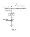
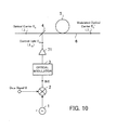
- FIG. 1 illustrates the optical-signal processing apparatus according to the first embodiment.
- the optical-signal processing apparatus of FIG. 1 comprises an oscillator 1, a multiplier 2, and an optical modulator 3.
- an optical combiner 4 and a nonlinear optical medium 5 are arranged in an optical transmission line 6, so that an optical carrier E s having the wavelength ⁇ s and propagating through the optical transmission line 6 passes through the optical combiner 4 and the nonlinear optical medium 5.
- the optical transmission line 6 is realized by, for example, an optical fiber.
- the optical carrier E s is, for example, continuous-wave (CW) light or control light modulated with an information (data) signal.
- CW continuous-wave
- the nonlinear optical medium 5 is, for example, a portion of the optical fiber realizing the optical transmission line 6.
- the nonlinear optical medium 5 may be a nonlinear optical fiber in which a nonlinear optical effect is enhanced.
- the optical combiner 4 optically combines the optical carrier E s and control light E ct which is outputted from the optical modulator 3 as explained below.
- the oscillator 1 generates a carrier signal having a RF (radio frequency) frequency.
- the carrier signal generated by the oscillator 1 and a data signal B (which represents information to be transmitted by multiplexing onto the optical carrier E s ) are inputted into the multiplier 2, the multiplier 2 modulates the inputted carrier with the inputted data signal B, so that a modulated signal B(f) is generated and outputted to the optical modulator 3.
- the optical modulator 3 receives the modulated signal B(f) and outputs the control light E ct corresponding to the modulated signal B(f), where the control light E ct has the wavelength ⁇ ct , which is different from the wavelength ⁇ s of the optical carrier E s .
- the optical combiner 4 optically combines the optical carrier E s (which is to propagate through the nonlinear optical medium 5) and the control light E ct (which is outputted from the optical modulator 3).
- the optical combiner 4 is, for example, an optical coupler.
- the optical carrier E s and the control light E ct are optically combined by the optical combiner 4
- the optical carrier E s undergoes cross phase modulation (XPM) with the control light E ct in the nonlinear optical medium 5, so that modulated optical carrier E s ' having the wavelength ⁇ s is outputted from the nonlinear optical medium 5, where the degree (magnitude) of XPM is proportional to the power of the control light E ct.
- XPM cross phase modulation
- the optical carrier E s undergoes cross phase modulation with the control light E ct (which is optically modulated on the basis of the modulated data signal B). Therefore, the optical-signal processing apparatus of FIG. 1 can multiplex the data signal B on the optical carrier E s propagating in the optical network, and enables transmission of the data signal B from an arbitrary place in the optical network.
- the polarization states of the control light E ct and the optical carrier E s inputted into the optical combiner 4 may be adjusted so as to realize desirable cross phase modulation.
- the polarization states of the control light E ct and the optical carrier E s may be adjusted so as to coincide.
- the degree of cross phase modulation realized when the polarization of the control light E ct is orthogonal to the polarization of the optical carrier E s is approximately 1/3 (-2 dB) lower than the degree of cross phase modulation realized when the polarization states of the control light E ct and the optical carrier E s coincide. Therefore, in the case where the polarization of the control light E ct is orthogonal to the polarization of the optical carrier E s , it is possible to compensate for the reduction in the degree of cross phase modulation by using a compensation circuit, a digital-signal processing circuit, or the like in a receiver after the optical carrier E s is converted into an electric signal and the electric signal is demodulated into the data signal B.
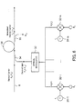
- FIG. 2 illustrates the optical-signal processing apparatus according to the second embodiment, which is a concrete example of the first embodiment.
- the optical modulator 3 in the first embodiment is realized by a laser diode (LD) 11, and the modulated signal B(f) is a driving current inputted into the LD 11 for direct optical modulation.
- the LD 11 outputs the control light E ct (optically modulated on the basis of the modulated data signal B).
- the LD 11 outputs the control light E ct , and the optical carrier E s undergoes cross phase modulation with the control light E ct in the nonlinear optical medium 5. Therefore, the optical-signal processing apparatus of FIG. 2 enables transmission of the data signal B from an arbitrary place in the optical network.
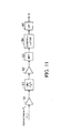
- FIG. 3 illustrates the optical-signal processing apparatus according to the third embodiment, which is another concrete example of the first embodiment.
- the optical modulator 3 in the first embodiment is realized by an external optical modulator 3-1 and a light source 12.
- the light source 12 is a laser diode (LD) which emits light having the wavelength ⁇ ct .
- the light emitted from the light source 12 and the modulated data signal B(f) outputted from the multiplier 2 are inputted into the external optical modulator 3-1.
- the external optical modulator 3-1 modulates the light emitted from the light source 12 with the modulated data signal B(f), and outputs the control light E ct having the wavelength ⁇ ct to the optical combiner 4.
- the external optical modulator 3-1 may be a Mach-Zehnder modulator or an LN (lithium niobate) modulator.
- the control light E ct are obtained by the optical modulation using the light source 12 and the external optical modulator 3-1.
- the optical-signal processing apparatus of FIG. 3 can output the control light E ct in response to modulated signals B(f) having higher frequencies than the optical-signal processing apparatus of FIG. 2 , in which the optical modulator (the LD 11) is directly modulated.
- the optical-signal processing apparatus of FIG. 2 can be constructed with a smaller number of components than the optical-signal processing apparatus of FIG. 3 . Therefore, the optical-signal processing apparatus of Fig. 2 can be constructed at lower cost than the optical-signal processing apparatus of FIG. 3 .
- FIG. 4 partially illustrates the optical network system according to the fourth embodiment.
- optical combiners 21 and 23, optical splitters 22 and 24, and nonlinear optical mediums 25 and 26 are arranged in an optical transmission line 6.
- Each of the optical combiners 21 and 23 is the optical combiner in one of the optical-signal processing apparatuses illustrated in FIGS. 1 , 2 , and 3 .
- each of the optical combiners 21 and 23 and the optical splitters 22 and 24 may be realized by, for example, a WDM (wavelength - divi s ion multiplexing) coupler.
- Each of the nonlinear optical mediums 25 and 26 corresponds to the nonlinear optical medium 5 illustrated in one of FIGS. 1 , 2 , and 3 . Further, in FIG.
- optical-signal processing apparatus connected to the optical combiner 21 is located at the (j-1)-th point in the optical network
- the optical-signal processing apparatus connected to the optical combiner 23 is located at the j-th point in the optical network.
- Control light E ct-(j-1) having the wavelength ⁇ ct-(j-1) is inputted into the optical combiner 21.
- the optical combiner 21 optically combines the control light E ct-(j-3) with modulated optical carrier E s-(j-2) which has the wavelength ⁇ s and propagates through the optical transmission line 6 (in which the nonlinear optical medium 25 is arranged).
- the modulated optical carrier E s-(j-2) ' undergoes cross phase modulation with the control light E ct-(j-1) in the nonlinear optical medium 25, so that modulated optical carrier E S-(j-2) ' having the wavelength ⁇ s and the control light E ct-(j-1) are outputted from the nonlinear optical medium 25.
- the optical splitter 22 splits the control light E ct-(j-1) from the output of the nonlinear optical medium 25. That is, the optical splitter 22 prevents propagation, beyond the optical splitter 22 to the nonlinear optical medium 26, of the control light E ct-(j-1) which is optically combined with the modulated optical carrier E s-(j-2) ' by the optical combiner 21.
- Control light E ct - j having the wavelength ⁇ ct-j is inputted into the optical combiner 23.
- the optical combiner 23 optically combines the control light E ct-j with modulated optical carrier E s-(j-1) ' which has the wavelength ⁇ s and propagates through the optical transmission line 6.
- the modulated optical carrier E s-(j-1) ' undergoes cross phase modulation with the control light E ct-j in the nonlinear optical medium 26, so that modulated optical carrier E s-(j-1) ' having the wavelength ⁇ s and the control light E ct-j are outputted from the nonlinear optical medium 26.
- the optical splitter 24 splits the control light E ct-j from the output of the nonlinear optical medium 26. That is, the optical splitter 24 prevents propagation, beyond the optical splitter 24 to a nonlinear optical medium in the following stage, of the control light E ct-j which is optically combined with the modulated optical carrier E s-(j-1) ' by the optical combiner 23.
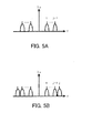
- FIGS. 5A and 5B indicate the spectra of modulated optical carriers propagating through the optical network of FIG. 4 .
- FIG. 5A indicates the allocation of the frequencies of the modulated optical carrier E s-(j-1) ' in the stage following the optical splitter 22
- FIG. 5B indicates the allocation of the frequencies of the modulated optical carrier E s-j ' in the stage following the optical splitter 24.
- the subband being added in the modulated optical carrier E s-(j-1) ' and carrying the j-th modulated data signal is indicated by the reference "j-1”
- the subband being added in the modulated optical carrier E s-j ' and carrying the j-th modulated data signal is indicated by the reference "j".
- the carrier frequency (i.e., the frequency of the carrier signal) of the optical-signal processing apparatus located at the (j-1)-th point i.e., the position of the optical combiner 21 illustrated in FIG. 4
- the modulated optical carrier E s-j ' carries the information corresponding to the j-th data signal in the subband "j" in addition to the information carried by the modulated optical carrier E s-(j-1) '.
- the above arrangement, in the optical network, of the plurality of optical-signal processing apparatuses having respectively different carrier frequencies enables optical frequency-division multiplexing, on a single optical carrier, of information (data signals) from the plurality of optical-signal processing apparatuses. That is, a plurality of data signals can be readily transmitted from a plurality of arbitrary places without providing more than one optical fiber or more than one optical carrier having more than one wavelength.
- optical-signal processing apparatus enables transmission of a plurality of data signals from each optical-signal processing apparatus through an optical network.
- FIG. 6 illustrates the optical-signal processing apparatus according to the fifth embodiment.
- the optical-signal processing apparatus of FIG. 6 comprises oscillators 31-1 to 31-n, multipliers 32-1 to 32-n, and an optical modulator 33.
- an optical combiner 34, an optical splitter 35, and a nonlinear optical medium 36 are arranged in an optical transmission line 6, and the optical carrier E s having the wavelength ⁇ s and propagating through the optical transmission line 6 passes through the optical combiner 34, the optical splitter 35, and the nonlinear optical medium 36.
- the optical transmission line 6 is realized by, for example, an optical fiber.
- the nonlinear optical medium 36 is, for example, a portion of the optical fiber realizing the optical transmission line 6.
- the nonlinear optical medium 36 may be a nonlinear optical fiber in which a nonlinear optical effect is enhanced.
- the optical combiner 34 optically combines the optical carrier E s and control light E ct which is outputted from the optical modulator 33 as explained below.
- Each of the optical combiner 34 and the optical splitter 35 may be realized by, for example, a WDM (wavelength-division multiplexing) coupler.
- the oscillators 31-1 to 31-n output to the multipliers 32-1 to 32-n n carrier signals (subcarrier signals in n channels) having different RF frequencies f 1 to f n , respectively.
- a plurality of data signals B 1 to B n each representing information to be transmitted through the optical transmission line 6 are inputted into the multipliers 32-1 to 32-n, respectively.
- the multipliers 32-1 to 32-n modulate the subcarrier signals with the data signals B 1 to B n , respectively, and obtain and combine a plurality of subcarrier-modulated data signals B 1 (f 1 ) to B n (f n ).
- the combined, subcarrier-modulated data signals are outputted to the optical modulator 33.
- the optical modulator 33 receives the combined, subcarrier-modulated data signals B 1 (f 1 ) to B n (f n ), generates control light E ct having the wavelength ⁇ ct and carrying (being optically modulated on the basis of) the subcarrier-modulated data signals B 1 (f 1 ) to B n (f n ), and outputs the control light E ct to the optical combiner 34.
- the optical modulator 33 is, for example, the LD 11 illustrated in FIG. 2 , or the external optical modulator 3-1 illustrated in FIG. 3 .
- the wavelength ⁇ ct of the control light E ct is different from the wavelength ⁇ s of the optical carrier E s .
- the optical combiner 34 optically combines the control light E ct with the optical carrier E s propagating through the optical transmission line 6 (connected to the nonlinear optical medium 36).
- the optical carrier E s and the control light E ct are optically combined by the optical combiner 34, the optical carrier E s undergoes cross phase modulation (XPM) with the control light E ct in the nonlinear optical medium 36, so that modulated optical carrier E s ' having the wavelength ⁇ s is outputted from the nonlinear optical medium 36, where the degree of XPM is proportional to the power of the control light E ct .
- XPM cross phase modulation
- the optical splitter 35 splits the control light E ct from the output of the nonlinear optical medium 36. That is, the optical splitter 35 prevents propagation, beyond the optical splitter 35 to a nonlinear optical medium in the following stage, of the control light E ct which is optically combined with the modulated optical carrier E s ' by the optical combiner 34.
- the optical-signal processing apparatus enables cross phase modulation of the optical carrier E s propagating through the optical transmission line 6, with the control light E ct which is optically modulated on the basis of the plurality of subcarrier-modulated signals B 1 (f 1 ) to B n (f n ) - Therefore, the optical-signal processing apparatus according to the fifth embodiment can transmit a plurality of data signals from arbitrary places.
- FIG. 7 partially illustrates the optical network system according to the sixth embodiment.
- the optical-signal processing apparatuses 42-1, ... , 42 - (j-1), 42-j, 42 -(j+1), ... , 42-m are arranged in the optical network.
- the optical-signal processing apparatuses 42-1, ... , 42 - (j-1), 42-j, 42-(j+1), ... , 42-m may be referred to as the first, ... , (j-1)-th, j-th, (j+1)-th, ... , m-th optical-signal processing apparatuses.
- Each of the optical-signal processing apparatuses 42-1, ... , 42-(j-1), 42-j, 42-(j+1), ... , 42-m contains a nonlinear optical medium.
- Each of the nonlinear optical mediums may be a nonlinear optical fiber in which a nonlinear optical effect is enhanced.
- Each of the optical-signal processing apparatuses 42-1, ... , 42 - (j-1), 42-j, 42 - (j+1), ... , 42-m has a construction similar to the optical-signal processing apparatus of FIG. 6 .
- the optical-signal processing apparatus 42-j comprises oscillators 51-1 to 51-n, multipliers 52-1 to 52-n , an optical modulator 53, an optical combiner 54, and an optical splitter 55.
- the frequencies of the subcarrier signals in each optical-signal processing apparatus arranged in the optical network are different from the frequencies of the subcarrier signals in any of the other optical-signal processing apparatuses in the optical network.
- the frequencies f 11 to f 1n are allocated to the subcarrier signals in the first optical-signal processing apparatus 42-1
- the frequencies f 21 to f 2n are allocated to the subcarrier signals in the second optical-signal processing apparatus 42-2
- the frequencies f m1 to f mn are allocated to the subcarrier signals in the m-th optical-signal processing apparatus 42-m.
- the number of the subcarrier signals in each optical-signal processing apparatus is identical (i.e., the number of channels is n) in the above example, generally, the number of the subcarrier signals in each optical-signal processing apparatus may be different.
- FIG. 8 indicates the distribution of the frequencies of the subcarrier-modulated data signals which are inserted from the optical-signal processing apparatuses 42-1 to 42-m into the optical network of FIG. 7 (and combined with the optical carrier E s ), where the subcarrier-modulated data signals are generated in the optical-signal processing apparatuses 42-1 to 42-m.
- FIG. 8 indicates the distribution of the frequencies of the subcarrier-modulated data signals which are inserted from the optical-signal processing apparatuses 42-1 to 42-m into the optical network of FIG. 7 (and combined with the optical carrier E s ), where the subcarrier-modulated data signals are generated in the optical-signal processing apparatuses 42-1 to 42-m.
- Band-1 indicates the extent of the frequencies of the subcarrier-modulated data signals carried by the control light which is outputted from the first optical-signal processing apparatus 42-1 and inserted into the optical network
- Band-2 indicates the range of the frequencies of the subcarrier-modulated data signals carried by the control light which is outputted from the second optical-signal processing apparatus 42-2 and inserted into the optical network
- Band-j indicates the range of the frequencies of the subcarrier-modulated data signals carried by the control light which is outputted from the j-th optical-signal processing apparatus 42-j and inserted into the optical network
- Band-m indicates the range of the frequencies of the subcarrier-modulated data signals carried by the control light which is outputted from the m-th optical-signal processing apparatus 42-m and inserted into the optical network.
- the subcarrier-modulated data signals B j1 (f j1 ) to B jn (f jn ) generated in the j-th optical-signal processing apparatus 42-j have frequencies in the range Band-j, which does not overlap the range of the frequencies of the subcarrier-modulated data signals generated in any of the other optical-signal processing apparatuses as indicated in FIG. 8 .
- the frequencies of the subcarrier- signals are allocated to the optical-signal processing apparatuses 42-1 to 42-m so that the range of the frequencies of the subcarrier-modulated data signals generated in each of the optical-signal processing apparatuses does not overlap the range of the frequencies of the subcarrier-modulated data signals generated in any of the other optical-signal processing apparatuses.
- the frequencies of the subcarrier-modulated data signals allocated to the optical-signal processing apparatuses 42-1 to 42-m increase in order of the locations of the optical-signal processing apparatuses in the above example, generally the allocation of the frequencies is arbitrary.
- the plurality of nonlinear optical mediums 43-1, ... , 43 - (j-1), 43-j, 43-(j+1), ... , 43-m and the plurality of optical-signal processing apparatuses 42-1 to 42-m are arranged in the optical network, and each optical-signal processing apparatus generates control light based on subcarrier-modulated data signals which are modulated with subcarrier signals having different frequencies, in order to realize cross phase modulation of the optical carrier with the control light.
- the optical network system facilitates transmission, from more than one arbitrary position, of a plurality of data signals.
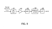
- FIG. 9 illustrates the receiver according to the seventh embodiment.
- the receiver of FIG. 9 comprises a photo diode (PD) 61, an amplifier 62, a band-pass filter (BPF) 63, demodulator 64, and a low-pass filter (LPF) 65.
- PD photo diode
- BPF band-pass filter
- LPF low-pass filter
- the PD 61 is a light receiving device which receives the (modulated) optical carrier E s , and converts the optical carrier E s into an electric signal, so that, for example, an electric signal representing n-channel subcarrier-modulated data signals are outputted from the PD 61.
- the amplifier 62 amplifies the electric signal outputted from the PD 61.
- the BPF 63 passes one or more portions, in one or more frequency ranges respectively centered at the frequencies of one or more carrier signals, of the electric signal amplified by the amplifier 62.
- the BPF 63 passes electric signals in the ranges respectively centered at the frequencies of the n corresponding subcarrier signals. That is, in this case, the portions, corresponding to the respective channels, of the electric signal outputted from the amplifier 62 are separated.
- the BPF 63 may pass portions of the electric signal corresponding to necessary channels only, instead of passing the portions of the electric signal corresponding to all the n channels.
- the demodulator 64 is a circuit which demodulates the one or more portions of the electric signal, for example, according to the manner of modulation of one or more data signals.
- the demodulator 64 is, for example, an envelope detector, a square-law detector, a phase detector, a frequency discriminator, or the like.
- the LPF 65 passes a low-frequency portion of each of the output channels of the demodulator 64.
- the receiver according to the seventh embodiment can demodulate one or more data signals transmitted by cross phase modulation in a nonlinear optical medium with control light, which is generated by modulation of one or more carrier signals with the one or more data signals.
- the PD 61 can output an electric signal in an intermediate frequency range.
- a receiver will be explained later with reference to FIG. 28 .
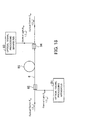
- FIG. 10 illustrates the optical-signal processing apparatus according to the eighth embodiment.
- the optical-signal processing apparatus according to the eighth embodiment is different from the first embodiment in that the control light is optically amplified.
- an optical amplifier 71 is arranged between the optical modulator 3 and the optical combiner 4.
- the optical amplifier 71 amplifies the control light E ct (outputted from the optical modulator 3), and outputs the amplified control light E ct to the optical combiner 4.
- the optimal amplifier 71 is, for example, an optical fiber amplifier, a semiconductor optical amplifier, an optical parametric amplifier, or the like. Since the control light E ct is amplified before being inputted into the nonlinear optical medium 5, the data signal B can be appropriately obtained by demodulation in a receiver.
- the optical carrier E s may be amplified.
- an optical amplifier may be arranged on the input side of the optical combiner 4 in the optical transmission line 6 illustrated in FIG. 10 so as to amplify the optical carrier E s .
- the data signal B can also be appropriately demodulated in a receiver.
- FIG. 11 illustrates the receiver according to the ninth embodiment, in which the optical carrier E s is amplified before being inputted into the PD 61. That is, in the receiver according to the ninth embodiment, an optical amplifier 72 is arranged on the input side of the PD 61. Thus, the optical amplifier 72 amplifies the optical carrier E s (which is transmitted through the optical transmission line 6 and a nonlinear optical medium) before the optical carrier E s is inputted into the PD 61.
- the optical amplifier 72 is, for example, an optical fiber amplifier, a semiconductor optical amplifier, an optical parametric amplifier, or the like.
- the optical carrier E s is amplified before being inputted into the PD 61 as explained above, it is possible to appropriately obtain the data signal B from the demodulator.
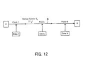
- FIG. 12 illustrates a first example of the optical network system according to the tenth embodiment containing optical-signal processing apparatuses.
- an optical-signal processing apparatus (which may or may not belong to an optical network system) is connected, at each of the points 1, ... , j, ... , N, to an optical transmission line 6 connecting a point A and a point B.
- the optical-signal processing apparatus connected to each of the points 1, ... , j, ... , N inserts control light conveying modulated data signals, into the optical transmission line 6 through the point so as to multiplex the modulated data signals with the optical carrier E s .
- the information represented by the modulated data signals 1, ... , N respectively inserted from the points 1, ... , N is, for example, information on sensors and/or monitors in the optical network, information on electric power in the optical network, information on users' requests in a local area network, and other information.
- the example of FIG. 12 can be applied to optical wirings interconnecting servers in a data center.
- FIG. 13 illustrates an example of a bidirectional optical transmission system to which the optical network system of FIG. 12 is applied.
- a carrier signal having the frequency f is modulated with information B 2 so as to generate an RF signal, and a combined signal is generated by combining baseband information B 1 with the RF signal, and is then inputted into an optical modulator.
- the optical modulator outputs modulated light (having the wavelength ⁇ B ) into the optical transmission line 6, so that the modulated light is transmitted to the point A.
- the terminal A at the point A splits the modulated light from the optical carrier E s , and receives the RF signal (modulated with the carrier signal having the frequency f) or the baseband signal.
- the optical carrier E s having the wavelength ⁇ s propagates from the terminal A to the terminal B, and the modulated data signals 1, ... , N are multiplexed on the optical carrier E s by inserting control light into the optical transmission line 6 from each of the optical-signal processing apparatuses at the points 1, ... , j, ... , N.
- the terminal B can split and receive the modulated data signals 1, ... , N from the optical carrier E s .
- the baseband information B 1 is, for example, a baseband signal and the like being transmitted in the conventional passive optical network (PON) or the like and having the transmission rate of 100Mb/s, 1Gb/s, 1OGb/s, or the like.
- the information B 2 may be an information signal having the bandwidth (bit rate) identical to or different from the baseband information B 1 .
- the degrees of modulation, the bit rates, the power, and the like of the baseband information B 1 and the information B 2 are adjusted so that the baseband information B 1 and the information B 2 can be received by the terminal A with similar reception sensitivities.
- FIG. 14 illustrates a second example of an optical network system according to the tenth embodiment containing optical-signal processing apparatuses.
- the optical carrier E s having the wavelength ⁇ s propagates in the anticlockwise direction through an optical transmission line 6 which forms a loop passing through the point A, and an optical-signal processing apparatus or an optical network system is connected to the optical transmission line 6 at each of arbitrary points 1, ... , j, ... , N.
- Modulated data signals 1, ... , N which are similar to the first example of FIG. 12 , are multiplexed on the optical carrier E s by inserting control light from the arbitrary points into the optical transmission line 6.
- the optical-signal processing apparatus or optical network system connected to the optical transmission line 6 can easily transmit information from arbitrary points.
- the optical network system according to the sixth embodiment needs neither more than one optical fiber nor more than one optical carrier having more than one wavelength even in the case where data signals from more than one source are transmitted, since data signals can be easily transmitted by modulating the data signals and multiplexing the modulated data signals on a single optical carrier E s propagating through an optical network.
- the data signals which are multiplexed on the optical carrier E s by other optical-signal processing apparatuses in the optical network systems illustrated in FIGS. 12 and 14 can be extracted and observed at an arbitrary point, for example, by a technique in which a portion of the optical carrier E s is extracted by tapping by use of a power branch circuit, or a technique in which continuous-wave (CW) light having a wavelength near the control light is combined with the optical carrier E s and idler light generated by four-wave mixing occurring in the optical fiber is extracted by an optical filter or a WDM coupler.
- CW continuous-wave
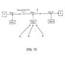
- FIG. 15 illustrates a first example of the optical network system according to the eleventh embodiment containing optical-signal processing apparatuses.
- an optical-signal processing apparatus (which may or may not belong to an optical network system) is connected, at each of the points 1, ... , j, ... , N, to an optical transmission line 6 connecting a point A and a point B.
- the collection may be made by wired or wireless communication.
- Each optical-signal processing apparatus j inserts control light (optically modulated on the basis of modulated data signals) into the optical transmission line 6 so as to multiplex the modulated data signals on the optical carrier E s , for example, as explained with reference to FIG. 6 .
- FIG. 16 illustrates a second example of an optical network system according to the eleventh embodiment containing optical-signal processing apparatuses.
- an optical-signal processing apparatus or an optical network system is connected to the optical transmission line 6 at each of arbitrary points 1, ... , j, ... , N.
- the subcarrier modulated data signals B j1 (f j1 ) to B jn (f jn ) are signals generated by modulating data signals B j1 to B jn on the carrier signals having the frequencies f j1 to f jn , respectively.
- the collection may be made by wired or wireless communication.
- each optical-signal processing apparatus j can insert the control light (optically modulated on the basis of the subcarrier modulated data signals) into the optical transmission line 6 so as to multiplex the modulated data signals on the optical carrier E s .
- the data signals are modulated in the sources (not shown) of the data signals. Therefore, the optical-signal processing apparatus or optical network system at each of arbitrary points 1, ... , N needs neither the oscillator nor the multiplier. Each optical-signal processing apparatus is required only to generate and output the control light based on the subcarrier modulated data signals by use of the optical modulator.
- a number of data signals are frequency-division multiplexed within a narrow bandwidth.
- FIGS. 17A and 17B indicate the allocations of the subcarrier frequencies for explaining operations of the optical-signal processing apparatus according to the twelfth embodiment.
- FIG. 17A indicates the allocation of the subcarrier frequencies in a common frequency-division multiplexing system
- FIG. 17B indicates the allocation of the subcarrier frequencies in a frequency-division multiplexing system used in the twelfth embodiment.
- the carrier spacing is set to 2Bd or greater in order to prevent crosstalk from adjacent channels.
- the carrier spacing is set to 2Bd or greater, the main lobe of the bandwidth of each of the modulated data signals can be separated from the main lobe of the bandwidth of one or two adjacent modulated data signals as indicated in FIG. 17A , so that satisfactory data transmission is enabled.
- the carrier spacing is set to ⁇ Bd ( ⁇ 2), and the bandwidth of each modulated data signal is limited by using a filter so that crosstalk does not occur even in the case where the carrier spacing is ⁇ Bd ( ⁇ 2).
- the bandwidths of the modulated data signals in the optical-signal processing apparatus illustrated in FIG. 6 can be limited by arranging low-pass filters (LPFs) which respectively limit the bandwidths of the data signals B 1 to B n before the data signals B 1 to B n are inputted into the multipliers 32-1 to 32-n so as to limit the bandwidths of the data signals B 1 to B n .
- LPFs low-pass filters
- the subcarrier-modulated data signals B 1 (f 1 ) to B n (f n ) inputted into the optical modulator 33 have the allocation of frequencies as indicated in FIG. 17B .
- band-pass filters which respectively limit the bandwidths of the subcarrier-modulated data signals B 1 (f 1 ) to B n (f n ) before the subcarrier-modulated data signals B 1 (f 1 ) to B n (f n ) are inputted into the optical modulator 33.
- the subcarrier-modulated data signals B 1 (f 1 ) to B n (f n ) inputted into the optical modulator 33 can also have the distribution of frequencies as indicated in FIG. 17B .
- an optical band-pass filter on the output side of the optical modulator 33 so as to limit the bandwidths of the components corresponding to the subcarrier-modulated data signals B 1 (f 1 ) to B n (f n ) in the control light E ct as indicated in FIG. 17B .
- the bandwidths of the modulated data signals can be reduced by use of the multi-level modulation or other types of optical multiplex transmission systems.
- the bandwidth limitation of the data signals by using band-pass filters or low-pass filters enables frequency-division multiplexing of a number of data signals within a narrow bandwidth.
- the above provision for the bandwidth limitation using band-pass filters or low-pass filters can be similarly applied to the optical network system illustrated in FIG. 7 .
- FIG. 18 illustrates the optical network system according to the thirteenth embodiment.
- optical couplers 82 and 84 and a nonlinear optical medium 85 are arranged in an optical transmission line 6.
- optical-signal processing apparatuses 81 and 83 are respectively connected to the optical couplers 82 and 84.
- optical carrier E 01 having the wavelength ⁇ 01 and an optical carrier E 02 having the wavelength ⁇ 02 propagate through the optical transmission line 6 and the nonlinear optical medium 85, where the direction of the propagation of the optical carrier E 01 is opposite to the direction of the propagation of the optical carrier E 02 , In FIG. 18 , the optical carrier E 01 propagates from the left to the right, and the optical carrier E 02 propagates from the right to the left.
- the optical transmission line 6 is realized by, for example, an optical fiber.
- the nonlinear optical medium 85 is, for example, a portion of the optical fiber realizing the optical transmission line 6. Alternatively, the nonlinear optical medium 85 may be a nonlinear optical fiber in which a nonlinear optical effect is enhanced.
- the optical-signal processing apparatus 81 is, for example, the optical-signal processing apparatus of FIG. 1 .
- the optical modulator in the optical-signal processing apparatus 81 outputs control light E S1 having the wavelength ⁇ S1 .
- the control light E S1 is generated by optical modulation based on a modulated data signal, which is generated by modulation of a carrier signal with a data signal.
- the optical coupler 82 optically combines the control light E S1 with the optical carrier E 01 propagating through the optical transmission line 6 before propagating through the nonlinear optical medium 85.
- the optical coupler 82 is, for example, a WDM coupler. Therefore, the optical carrier E 01 undergoes cross phase modulation (XPM) with the control light E S1 in the nonlinear optical medium 85, so that the modulated data signal is multiplexed on the optical carrier E 01 .
- XPM cross phase modulation
- the optical-signal processing apparatus 83 is, for example, the optical-signal processing apparatus of FIG. 1 .
- the optical modulator in the optical-signal processing apparatus 83 outputs control light E S2 having the wavelength ⁇ S2 .
- the control light E S2 is generated by optical modulation based on a modulated data signal, which is generated by modulation of a carrier signal with a data signal.
- the optical coupler 84 optically combines the control light E S2 with the optical carrier E 02 propagating through the optical transmission line 6 before propagating through the nonlinear optical medium 85.
- the optical coupler 84 is, for example, a WDM coupler. Therefore, the optical carrier E 02 undergoes cross phase modulation (XPM) with the control light E S2 in the nonlinear optical medium 85, so that the modulated data signal is multiplexed on the optical carrier E 02 .
- XPM cross phase modulation
- FIG. 19 indicates an example allocation of the wavelengths ⁇ 01 and ⁇ 02 of the optical carriers E 01 and E 02 and the wavelengths ⁇ S1 and ⁇ S2 of the control light E S1 and E S2 with respect to the cut-off wavelength of the optical couplers 82 and 84 in the optical network system of FIG. 18 .
- the abscissa corresponds to the wavelength
- the cut-off wavelength of the optical couplers 82 and 84 is indicated by the downwards dashed arrow A11.
- the optical coupler 82 has input ports for the optical carrier E 01 and the control light E S1
- the optical coupler 84 has input ports for the optical carrier E 02 and the control light E S2.
- the optical couplers 82 and 84 pass the optical carriers having the wavelengths smaller than the cut-off wavelength when the optical carriers are inputted from the input ports for the optical carriers E 01 and E 02 , and cut (split) off the control light having wavelengths greater than the cut-off wavelength when the control light is inputted from the input ports for the optical carriers E 01 and E 02 .
- the optical couplers 82 and 84 pass the control light having the wavelengths greater than the cut-off wavelength when the control light is inputted from the input ports for the control light E S1 and E S2, and cut (split) off the optical carriers having the wavelengths smaller than the cut-off wavelength when the optical carriers are inputted from the input ports for the control light E S1 and Es 2 .
- the wavelengths ⁇ 01, and ⁇ 02 of the optical carriers E 01 and E 02 are allocated within the transmission bandwidths of the input ports for the optical carriers E 01 and E 02 in the optical couplers 82 and 84, respectively, and the wavelengths ⁇ S1 and ⁇ S2 of the control light E S1 and E S2 are allocated outside the transmission bandwidths of the input ports for the optical carriers E 01 and E 02 in the optical couplers 82 and 84, respectively.
- the optical carriers E 01 and E 02 and the control light E S1 and E S2 can be efficiently inputted into the nonlinear optical medium 85, so that the optical carries E 01 and E 02 can respectively undergo cross phase modulation with the control light E S1 and E S2 with almost no loss.
- each of the WDN couplers can be realized by a combination of an optical power combiner and an optical band-pass filter.
- the optical power combiner causes power loss, so that the power is greatly lost compared with the case in which WDM coupler is used.
- the optical carrier E 01 propagating through the nonlinear optical medium 85 in one direction undergoes cross phase modulation with the control light E S1 which is generated by optical modulation with a subcarrier-modulated data signal, which is generated by modulating a carrier signal with a data signal
- the optical carrier E 02 propagating through the nonlinear optical medium 85 in the opposite direction undergoes cross phase modulation with the control light E S2 which is also generated by optical modulation with a subcarrier-modulated data signal, which is generated by modulating a carrier signal with a data signal.
- each of the optical-signal processing apparatuses 81 and 83 in FIG. 18 is assumed to be the optical-signal processing apparatus of FIG. 1 in the above explanations, the optical-signal processing apparatuses 81 and 83 may be any of the optical-signal processing apparatuses illustrated in FIGS. 2 , 3 , and 10 .
- a light beat which is obtained as a frequency-difference component when two light waves having different wavelengths (frequencies) are optically combined may be used as the control light.
- optical phase modulation can be performed by using the above frequency-difference component as a subcarrier signal, and frequency-division multiplexing of signals with higher data rates can be performed by using wide-band cross phase modulation at higher frequencies.
- frequency-division multiplexing of signals in a greater number of channels can be performed by using wide-band cross phase modulation.
- optical network system according to the fourteenth embodiment is explained below.
- the optical network system according to the fourteenth embodiment is different from the optical network system according to the thirteenth embodiment in that optical couplers which split off the control light from the optical carriers are arranged in the optical transmission line 6 in addition to the arrangement in the optical network system according to the thirteenth embodiment.
- FIG. 20 illustrates the optical network system according to the fourteenth embodiment.
- optical couplers 82a, 82b, 84a, and 84b and the nonlinear optical medium 85 are arranged in the optical transmission line 6.
- optical-signal processing apparatuses 81 and 83 are respectively connected to the optical couplers 82a and 84a.
- the optical coupler 82a optically combines the control light E S1 (which is outputted from the optical-signal processing apparatus 81) with the optical carrier E 01 propagating through the optical transmission line 6 (connected to the nonlinear optical medium 85).
- the optical coupler 82a is, for example, a WDM coupler.
- the optical coupler 82b splits the control light E S1 from the optical carrier E 01 propagating through the optical transmission line 6.
- the optical coupler 82b prevents propagation of the control light E S1 to the stage beyond the nonlinear optical medium 85.
- the optical coupler 82b is, for example, a WDM coupler.
- the optical coupler 84a optically combines the control light E S2 (which is outputted from the optical-signal processing apparatus 83) with the optical carrier E 02 propagating through the optical transmission line 6 (connected to the nonlinear optical medium 85).
- the optical coupler 84a is, for example, a WDM coupler.
- the optical coupler 84b splits the control light E S2 from the optical carrier E 02 propagating through the optical transmission line 6 (connected to the nonlinear optical medium 85).
- the optical coupler 84b prevents propagation of the control light E S2 to the stage beyond the nonlinear optical medium 85.
- the optical coupler 84b is, for example, a WDM coupler.
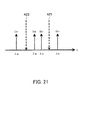
- FIG. 21 indicates an example allocation of the wavelengths ⁇ 01 and ⁇ 02 of the optical carriers E 01 and E 02 and the wavelengths ⁇ S1 and ⁇ S2 of the control light E S1 and E S2 with respect to the cut-off wavelength of the optical couplers 82a and 82b and the cut-off wavelength of the optical couplers 84a and 84b.
- the abscissa corresponds to the wavelength
- the cut-off wavelength of the optical couplers 82a and 82b is indicated by the downwards dashed arrow A21
- the cut-off wavelength of the optical couplers 84a and 84b is indicated by the downwards dashed arrow A22.
- the optical couplers 82a and 82b pass the control light having wavelengths smaller than the cut-off wavelength of the optical couplers 82a and 82b indicated by the downwards dashed arrow A21, and cut (split) off the control light having wavelengths equal to or greater than the cut-off wavelength of the optical couplers 82a and 82b.
- the optical couplers 84a and 84b pass the control light having wavelengths greater than the cut-off wavelength of the optical couplers 84a and 84b indicated by the downwards dashed arrow A22, and cut (split) off the control light having wavelengths equal to or smaller than the cut-off wavelength of the optical couplers 84a and 84b.
- the cut-off wavelength of the optical couplers 84a and 84b indicated by the downwards dashed arrow A22 is assumed to be smaller than the cut-off wavelength of the optical couplers 82a and 82b indicated by the downwards dashed arrow A21, so that the wavelengths between the cut-off wavelength indicated by the downwards dashed arrow A21 and the cut-off wavelength indicated by the downwards dashed arrow A22 constitute the transmission bandwidth for the optical carriers.
- the wavelengths ⁇ 01 and ⁇ 02 of the optical carriers E 01 and E 02 are allocated within the above transmission bandwidth, and the wavelengths ⁇ S1 and ⁇ S2 of the control light E Sl and the control light E S2 are allocated at symmetric positions on both sides of the transmission bandwidth along the wavelength axis as indicated in FIG. 21 .
- the optical carriers E 01 and E 02 and the wavelengths ⁇ S1 and ⁇ S2 of the control light E S1 and E S2 , and the cut-off wavelengths in the optical couplers 82a, 82b, 84a, and 84b are set as explained above (as indicated in FIG. 19 ), the optical carriers E 01 and E 02 and the control light E S1 and E S2 can be efficiently inputted into the nonlinear optical medium 85, so that the optical carriers E 01 and E 02 can respectively undergo cross phase modulation with the control light E S1 and E S2 with almost no loss.
- control light E S1 , and the control light E S2 used for the cross phase modulation are cut off by the optical couplers 82b and 84b so that the control light E S1 and E S2 do not propagate through the optical transmission line 6 beyond optical couplers 82b and 84b, respectively.
- the wavelengths ⁇ S1 and ⁇ S2 of the control light E S1 and the control light E S2 are arranged at symmetric positions on both sides of the transmission bandwidth along the wavelength axis. Therefore, it is possible to efficiently use the transmission bandwidth and flexibly allocate the wavelengths.
- the optical network system according to the fifteenth embodiment contains a plurality of optical network systems each having the configuration according to the thirteenth embodiment for optical frequency-division multiplexing of data signals.
- FIG. 22 illustrates the optical network system according to the fifteenth embodiment.
- optical couplers 92-1, . . . ,92-j, . . . , 92-N, 94-1, . . . , 94-j, . . . , 94-N and the nonlinear optical mediums 95-1, . . . , 95-j, . . . , 95-N are arranged in the optical transmission line 6.
- optical-signal processing apparatuses 91-1, . . . , 91-j, . . . , 91-N, 93-1, . . . , 93-j, . . . , 93-N are respectively connected to the optical couplers 92-1, . . . , 92-j, . . . , 92-N, 94-1, . . . , 94-j , . . . , 94-N.
- the terminals A and B are connected to both ends of the optical transmission line 6.
- the optical carrier E 01 having the wavelength ⁇ 01 propagates through the optical transmission line 6 from the terminal A to the terminal B
- the optical carrier E 02 having the wavelength ⁇ 02 propagates through the optical transmission line 6 from the terminal B to the terminal A.
- the optical carriers E 01 , and E 02 are detected in the terminals B and A, respectively.
- the N subsystems each being similar to the optical network system illustrated in FIG. 18 are arranged along the optical transmission line 6.
- the N subsystems may be referred to as the first, second, ... , j-th, ... , N-th subsystems from the left to the right in FIG. 22 .
- Different carrier frequencies are allocated to the optical-signal processing apparatuses 91-1, ... , 91-j, ... , 91-N, 93-1, ... , 93-j, ... , 93-N for the carrier signals, so that each subsystem outputs control light optically modulated on the basis of a subcarrier-modulated data signal which is modulated by use of a carrier signal having a different frequency.
- the frequency f 11 is allocated for the carrier signal in the first subsystem
- the frequency f 1j is allocated for the carrier signal in the j-th subsystem
- the frequency f 1N is allocated for the carrier signal in the N-th subsystem.
- 91-N generate control light E 11 to E S1N respectively having the wavelengths ⁇ S11 and ⁇ S1N and being optically modulated on the basis of subcarrier-modulated data signals generated by modulation by use of carrier signals having the different frequencies f 11 to f 1N , and inserts the control light E S11 to E S1N into the optical transmission line 6 so as to optically combine the control light E S11 to E S1N with the optical carrier E 01 .
- the frequency f 21 is allocated for the carrier signal in the first subsystem
- the frequency f 2j is allocated for the carrier signal in the j-th subsystem
- the frequency f 2N is allocated for the carrier signal in the N-th subsystem.
- 93-N generate control light E S21 to E S2N respectively having the wavelengths ⁇ S21 and ⁇ S2N and being optically modulated on the basis of subcarrier-modulated data signals generated by modulation by use of carrier signals having the different frequencies f 21 to f 2N , and inserts the control light E S21 to E S2N into the optical transmission line 6 so as to optically combine the control light E S21 to E S2N with the optical carrier E 02 .
- FIG. 23 indicates the j-th subsystem illustrated in FIG. 22 and the spectra of the optical carriers E 01 and E 02 propagating on the upstream side and downstream side of the j-th subsystem illustrated in FIG. 22 in the direction from the terminal A to the terminal B and in the direction from the terminal B to the terminal A.
- the reference 101 indicates the spectrum of the optical carrier E 01 incoming into the j-th subsystem illustrated in FIG. 22 in the direction from the terminal A to the terminal B
- the reference 102 indicates the spectrum of the optical carrier E 01 outgoing from the j-th subsystem illustrated in FIG. 22 in the direction from the terminal A to the terminal B.
- the frequency of the carrier signal used in modulation of a j-th data signal to be transmitted from the j-th subsystem toward the terminal B is different from the frequency of the carrier signal used in modulation of the data signal to be transmitted from the (j-1)-th subsystem toward the terminal B.
- a component carrying the j-th data signal is added to the optical carrier E 01 in the subband indicated by the reference "1j" in the spectrum 102 in FIG. 23 .
- the arrangement of the j-th subsystem enables addition of the component carrying the j-th data signal (modulated with the carrier signal having the frequency f ij ) to the optical carrier E 01 .
- the reference 103 indicates the spectrum of the optical carrier E 02 incoming into the j-th subsystem illustrated in FIG. 22 in the direction from the terminal B to the terminal A
- the reference 104 indicates the spectrum of the optical carrier E 02 outgoing from the j-th subsystem illustrated in FIG. 22 in the direction from the terminal B to the terminal A.
- the frequency of the carrier signal used in modulation of a j-th data signal to be transmitted from the j-th subsystem toward the terminal A is different from the frequency of the carrier signal used in modulation of the data signal to be transmitted from the (j-1)-th subsystem toward the terminal B.
- a component carrying the j-th data signal is added to the optical carrier E 02 in the subband indicated by the reference "2j" in the spectrum 104 in FIG. 23 .
- the arrangement of the j-th subsystem enables addition of the component carrying the j-th data signal (modulated with the carrier signal having the frequency f 2j ) to the optical carrier E 02 .
- the arrangement of the plurality of optical-signal processing apparatuses which respectively use carrier signals having different frequencies enables frequency-division multiplexing of carrier-modulated data signals on the optical carriers E 01 and E 02 respectively propagating in opposite directions.
- the optical network system according to the fifteenth embodiment needs neither more than one optical fiber nor more than one optical carrier having more than one wavelength even in the case where data signals from more than one source are transmitted.
- the N subsystems constituting the optical network system according to the fifteenth embodiment are not limited to the optical network system illustrated in FIG. 18 , and may be, for example, the optical network system illustrated in FIG. 20 .
- FIG. 24 illustrates the optical network system according to the sixteenth embodiment.
- the optical network system of FIG. 24 includes n 1 oscillators 111-1 to 111-n 1 , n 2 oscillators 121-1 to 121-n 2 , n 1 multipliers 112-1 to 112-n 1 , n 2 multipliers 122-1 to 122 ⁇ n 2 , optical modulators 113 and 123, optical couplers 114 and 124, and a nonlinear optical medium 130 are arranged in an optical transmission line 6, and the optical carriers E 01 and E 02 having the wavelengths ⁇ 01 and ⁇ 02 propagate through the optical transmission line 6 in opposite directions, respectively.
- the oscillators 111-1 to 111-n 1 output to the multipliers 112-1 to 112-n 1 n 1 carrier signals (subcarrier signals in n 1 channels) having different RF frequencies f 11 to f 1n1 , respectively.
- a plurality of data signals B 11 to B 1n1 each representing information to be transmitted through the optical transmission line 6 in a direction (i.e., the direction from the left to the right in FIG. 24 ) are inputted into the multipliers 112-1 to 112-n 1 , respectively.
- the multipliers 112-1 to 112-n 1 modulate the subcarrier signals with the data signals B 11 , to B 1n1 , respectively, and obtain and combine a plurality of subcarrier-modulated data signals B 11 (f 11 ) to B 1n1 (f 1n1 ).
- the combined, subcarrier-modulated data signals are outputted to the optical modulator 113.
- the optical modulator 113 receives the combined, subcarrier-modulated data signals B 11 (f 11 ) to B 1n1 (f 1n1 ), generates control light E S1 having the wavelength ⁇ S1 , and carrying the subcarrier-modulated data signals B 11 (f 11 ) to B 1n1 (f 1n1 ), and outputs the control light E S1 to the optical coupler 114.
- the optical modulator 113 is, for example, the LD 11 illustrated in FIG. 2 or the external optical modulator 11-1 illustrated in FIG. 3 .
- the optical coupler 114 optically combines the control light E S1 with the optical carrier E 01 propagating through the optical transmission line 6 (connected to the nonlinear optical medium 130).
- the optical coupler 114 is, for example, a WDM coupler.
- the optical carrier E 01 and the control light E S1 are optically combined by the optical coupler 114, the optical carrier E 01 . undergoes cross phase modulation (XPM) with the control light E S1 , in the nonlinear optical medium 130, so that the subcarrier-modulated data signals B 11 (f 11 ) to B 1n1 (f 1n1 ) are frequency-division multiplexed on the optical carrier E 01 , and the modulated optical carrier E 01 is outputted onto the optical transmission line 6.
- XPM cross phase modulation
- the oscillators 121-1 to 121-n 2 output to the multipliers 122-1 to 122-n 2 n 2 carrier signals (subcarrier signals in n 2 channels) having different RF frequencies f 21 to f 2n2 , respectively.
- a plurality of data signals B 21 to B 2n2 each representing information to be transmitted through the optical transmission line 6 in the opposite direction (i.e., the direction from the right to the left in FIG. 24 ) are inputted into the multipliers 122-1 to 122-n 2 , respectively.
- the multipliers 122-1 to 122-n 2 modulate the subcarrier signals with the data signals B 21 to B 2n2 , respectively, and obtain and combine a plurality of subcarrier-modulated data signals B 21 (f 21 ) to B 2n2 (f 2n2 ).
- the combined, subcarrier-modulated data signals are outputted to the optical modulator 123.
- the optical modulator 123 receives the combined, subcarrier-modulated data signals B 21 (f 21 ) to B 2n2 (f 2n2 ), generates control light E S2 having the wavelength ⁇ S2 and carrying the subcarrier-modulated data signals B 21 (f 21 ) to B 2n2 (f 2n2 ), and outputs the control light E S2 to the optical coupler 124.
- the optical modulator 123 is, for example, the LD 11 illustrated in FIG. 2 or the external optical modulator 11-1 illustrated in FIG. 3 .
- the optical coupler 124 optically combines the control light E S2 with the optical carrier E 02 propagating through the optical transmission line 6 (connected to the nonlinear optical medium 130).
- the optical coupler 124 is, for example, a WDM coupler.
- the optical carrier E 02 and the control light E S2 are optically combined by the optical coupler 124, the optical carrier E 02 undergoes cross phase modulation (XPM) with the control light E S2 in the nonlinear optical medium 130, so that the subcarrier-modulated data signals B 21 (f 21 ) to B 2n2 (f 2n2 ) are multiplexed on the optical carrier E 02 , and the modulated optical carrier E 02 is outputted onto the optical transmission line 6.
- XPM cross phase modulation
- the optical couplers 114 and 124 have the wavelength characteristics similar to the wavelength characteristics of the optical couplers 82 and 84 in the optical network system of FIG. 18 (which are explained before with reference to FIG. 19 ).
- additional optical couplers for splitting off the control light E S1 and E S2 from the optical carriers E 01 and E 02 like the optical couplers 82b and 84b in the optical network system of FIG. 20 (which are explained before with reference to FIG. 21 ).
- the optical carrier E 01 (propagating through the optical transmission line 6 in a direction) undergo, in the nonlinear optical medium 130, cross phase modulation with the control light E S1 carrying the subcarrier-modulated data signals B 11 (f 11 ) to B 1n1 (f 1n1 ), and the optical carrier E 02 (propagating through the optical transmission line 6 in the opposite direction) undergo, in the nonlinear optical medium 130, cross phase modulation with the control light E S2 carrying the subcarrier-modulated data signals B 21 (f 21 ) to B 2n2 (f 2n2 ). Therefore, the optical network system according to the sixteenth embodiment facilitates bidirectional transmission of a plurality of data signals from an arbitrary position.
- optical network more than one optical network system each having the construction illustrated in FIG. 24 .
- the frequencies of the subcarrier signals in each subsystem are allocated so as not to overlap with the frequencies of the subcarrier signals in the other subsystems.
- the manner of modulation of the subcarrier signals with the data signals B 11 to B 1n1 and B 21 to B 2n2 may not be limited to the multiplying using the multipliers 112-1 to 112-n 1 and the multipliers 122-1 to 122-n2 as illustrated in FIG. 24 , and the data signals B 11 to B 1n1 and B 21 to B 2n2 may by modulated by amplitude modulation, phase modulation, frequency modulation, or multi-level modulation based on one or a combination of amplitude modulation, phase modulation, and frequency modulation. Moreover, it is possible to modulate the data signals B 11 to B 1n1 and B 21 to B 2n2 so as to realize orthogonal frequency-division multiplexing.
- optical network system as a first variation of the thirteenth embodiment is explained below.
- the optical carrier E 02 is optically combined with the optical carrier E 01 in a first terminal, and is then transmitted to a second terminal, which is located on the downstream side of the optical carrier E 01 .
- FIG. 25 illustrates the optical network system as the first variation of the optical network system of FIG. 18 .
- the optical network system illustrated in FIG. 25 comprises terminals 150 and 160 and an optical fiber 171 connecting the terminals 150 and 160.
- the terminal 150 comprises a circulator 151, an optical coupler 152, and an optical combiner 153.
- the optical coupler 152 is, for example, a WDM coupler.
- the optical carrier E 01 is inputted from a light source into the circulator 151 in the terminal 150, where the optical carrier E 01 has the wavelength ⁇ 01 .
- the light source is provided in the terminal 150.
- the circulator 151 receives the optical carrier E 01 and outputs the optical carrier E 01 to the optical coupler 152.
- the circulator 151 also receives the optical carrier E 02 which is transmitted from the terminal 160 and modulated.
- the circulator 151 outputs the modulated optical carrier E 02 from a port which is different from the port through which the optical carrier E 01 is received.
- the optical coupler 152 optically combines control light E S1 with the optical carrier E 01 .
- the control light E S1 is outputted from an optical-signal processing apparatus (not shown) in the terminal 150.
- the optical-signal processing apparatus has a construction similar to the optical-signal processing apparatus 81 illustrated in FIG. 18 .
- the optical carrier E 01 undergoes cross phase modulation with control light E S1 in the optical fiber 171 or in the nonlinear fiber (not shown), so that a modulated data signal is multiplexed on the optical carrier E 01 .
- the optical combiner 153 optically combines the optical carrier E 02 with the optical carrier E 01 outputted from the optical coupler 152. Although not shown, another light source which outputs the optical carrier E 02 is provided in the terminal 150.
- the terminal 160 comprises a circulator 161, an optical coupler 162, and an optical fiber 163.
- the optical coupler 162 is, for example, a WDM coupler.
- the optical carrier E 02 which is optically combined with the optical carrier E 01 in the terminal 150 and transmitted to the terminal 160 is inputted into the circulator 161 in the terminal 160.
- the circulator 161 receives the optical carrier E 02 and outputs the optical carrier E 02 to the optical coupler 162.
- the circulator 161 also receives an optical carrier E 02 which is cross-phase modulated in the optical fiber 163, and outputs the cross-phase-modulated optical carrier E 02 to the optical fiber 171.
- the optical coupler 162 optically combines control light E S2 with the optical carrier E 02 outputted from the circulator 161, where the control light E S2 is outputted from an optical-signal processing apparatus (not shown) in the terminal 160.
- the optical-signal processing apparatus has a construction similar to the optical-signal processing apparatus 83 illustrated in FIG. 18 .
- the optical carrier E 02 optically combined with the control light E S2 undergoes cross phase modulation with control light E S2 in the optical fiber 163, so that a modulated data signal is multiplexed on the optical carrier E 02 .
- the optical fiber 163 is an optical fiber provided for modulation.
- the modulated data signal is multiplexed on the optical carrier E 02 by the cross phase modulation.
- the cross-phase-modulated optical carrier E 02 is outputted to the circulator 161.
- the optical carrier E 02 is optically combined with the optical carrier E 01 in the terminal 150, and is then transmitted from the terminal 150 to the terminal 160 through the optical fiber 171.
- the optical carrier E 02 transmitted to the terminal 160 is optically combined with the control light E S2 in the terminal 160, and the modulated data signal is multiplexed on the optical carrier E 02 by the cross phase modulation in the optical fiber 163.
- the cross-phase-modulated optical carrier E 02 is transmitted through the optical fiber 171 to the terminal 150.
- the arrangement of FIG. 25 can be used in the case where the light source for the optical carrier E 02 is desired to be arranged in the terminal 150 instead of the terminal 160.
- optical carrier E 02 it is possible to split the optical carrier E 02 from the optical carrier E 01 before the control light E S2 is optically combined with the optical carrier E 02 . Furthermore, it is possible to arrange additional optical couplers on both sides of the optical fiber 171 as the optical couplers 82b and 84b arranged on both sides of the optical fiber 171 in the optical network system of FIG. 20 .
- FIG. 26 illustrates the second variation of the optical network system of FIG. 18 .
- the second variation is different from the first variation in that N terminals B1, B2, . . . , BN including the terminal 160 are arranged opposite to the terminal 150 in the second variation.
- the terminal 160 corresponds to the terminal B1, and the terminals B2 and BN respectively bear the references 181 and 182.
- Each of the terminals B1, B2, . . . , BN contains an optical-signal processing apparatus (not shown).
- FIG. 26 illustrates the second variation of the optical network system of FIG. 18 .
- N terminals B1, B2, . . . , BN including the terminal 160 are arranged opposite to the terminal 150 in the second variation.
- the terminal 160 corresponds to the terminal B1
- the terminals B2 and BN respectively bear the references 181 and 182.
- Each of the terminals B1, B2, . . . , BN contains an optical-signal processing apparatus (not shown).
- optical signals transmitted from the terminal 150 through the optical fiber 171 are distributed to the N terminals B1, B2 , . . . , BN.
- different frequencies are allocated for the carrier signals to the optical-signal processing apparatuses in the terminals B1 , B2 , . . , BN. That is, the control light with which the optical carrier E 02 is cross-phase modulated in each of the terminals B1, B2, . . . , BN is optically modulated on the basis of a subcarrier modulated data signal which is modulated with a carrier signal having a different frequency.
- the terminal 150 transmits data to the N terminals B1, B2, ... , BN by using the optical carrier E 01 , and also transmits the optical carrier E 02 to the N terminals B1, B2 , . . . , BN by optically combining the optical carrier E 02 with the optical carrier E 01 . Then, each of the terminals B1, B2, . . . , BN multiplexes data on the optical carrier E 02 by using the control light, and the optical carrier E 02 on which the data is multiplexed and which is outputted from each of the terminals B1, B2, . . .
- BN undergoes power combining, and is transmitted through the optical fiber 171 to the terminal 150, where the multiplexing of the data is realized in each of the terminals B1 , B2, . . . , BN by cross phase modulation with the control light, which is modulated by using a different carrier frequency.
- FIG. 27 illustrates the third variation of the optical network system of FIG. 18 .
- the third variation is different from the first variation in that N terminals B1, B2, . . . , BN are arranged opposite to the terminal 150' in the third variation.
- the terminals B1 , B2, and BN respectively bear the references 190, 201, and 202.
- optical signals transmitted from the terminal 150' through the optical fiber 171 are distributed to the N terminals B1, B2, BN.
- Each of the terminals B1, B2, . . . , BN contains an optical-signal processing apparatus (not shown). As explained for the fifteenth and sixteenth embodiments, different frequencies are allocated for the carrier signals to the optical-signal processing apparatuses in the terminals B1 B2 , . . . , BN. That is, control light with which the optical carrier E 02 is cross-phase modulated in each of the terminals B1 , B2 , . . . , BN is optically modulated on the basis of a subcarrier modulated data signal which is modulated with a carrier signal having a different frequency.
- the terminal 150' in the optical network system of FIG. 27 is different from the terminal 150 in the optical network system of FIG. 25 in that the terminal 150' does not comprise the optical combiner 153, i.e., the terminal 150' does not optically combine the optical carrier E 02 with the optical carrier E 01 and does not transmit the optical carrier E 02 .
- the terminal B1 receives the optical carrier E 01 from the terminal 150' through the optical fiber 171 and comprises an optical coupler 191 and an optical fiber 192.
- the optical coupler 191 optically combines the control light E S2 (having the wavelength ⁇ S2 ) with the optical carrier E 02 (having the wavelength ⁇ 02 ), where the control light E S2 is outputted from an optical-signal processing apparatus arranged in the terminal B1.
- the optical-signal processing apparatus has a construction similar to the optical-signal processing apparatus 83 illustrated in FIG. 18 .
- the optical carrier E 02 may be externally inputted into the terminal B1 , or the terminal B1 may comprise a light source which outputs the optical carrier E 02 .
- the optical carrier E 02 optically combined with the control light E S2 undergoes cross phase modulation with the control light E S2 in the optical fiber 192, so that the modulated data signal is frequency-division multiplexed on the optical carrier E 02 .
- the optical fiber 192 is an optical fiber provided for modulation.
- the modulated data signal is frequency-division multiplexed on the optical carrier E 02 by the cross phase modulation.
- the cross-phase-modulated optical carrier E 02 is outputted to the terminal B2.
- Each of the terminals B2 , . . . , BN receives the optical carrier E 01 , from the terminal 150' through the optical fiber 171 and comprises an optical coupler similar to the optical coupler 191 and an optical fiber similar to the optical fiber 192.
- the optical coupler in each terminal Bj optically combines the control light (which is outputted from the optical-signal processing apparatus in the terminal Bj) with the optical carrier E 02 received from the terminal Bj-1.
- the optical carrier E 02 optically combined with the control light undergoes cross phase modulation in the optical fiber in the terminal Bj, so that a modulated data signal is multiplexed on the optical carrier E 02 .
- each of the terminals B1 , B2 , . . . , BN multiplexes data on the optical carrier E 02 by using the control light
- the optical carrier E 02 on which the data is multiplexed in the terminal BN is transmitted through the optical fiber 171 to the terminal 150', where the multiplexing of the data is realized in each of the terminals B1, B2 , . . . , BN by the cross phase modulation with the control light modulated by using a different carrier frequency.
- the optical fiber for modulation is arranged in each of the N terminals B1, B2, . . . , BN in order to perform cross phase modulation and realize frequency-division multiplexing
- a common optical fiber for modulation collect the control light from each of the terminals B1, B2, . . . , BN-1 into the terminal BN, and perform cross phase modulation with the control light from each of the terminals B1, B2, . . . , BN-1 in the common optical fiber in the terminal BN so as to realize the optical frequency-division multiplexing.
- FIG. 28 illustrates the receiver according to the seventeenth embodiment.
- the receiver of FIG. 28 is different from the receiver illustrated in FIG. 9 in comprising a laser diode (LD) 131 and an optical combiner 132 in addition to the constituents of the receiver of FIG. 9 .
- the LD 131 outputs local light E LO
- the optical combiner 132 optically combines the local light E LO with optical carrier E 01 or E 02 which is to be received by the PD 61.
- the frequency of the local light E LO is differentiated from the frequency of the optical carrier E 01 or E 02 by a desired detuning frequency (f if ).
- the PD 61 can output an electric signal in an intermediate frequency range.
- the receiver of FIG. 28 can demodulate the electric signal and obtain one or more data signals which are cross-phase modulated in a nonlinear optical medium with the control light optically modulated on the basis of one or more subcarrier-modulated data signals.
- receiver of FIG. 28 as well as the receivers of FIGS. 9 and 11 , can be used in either of unidirectional transmission and bidirectional transmission.
- the eighteenth embodiment is characterized in feedback processing performed in the optical-signal processing apparatus.
- FIG. 29 illustrates the optical-signal processing apparatus according to the eighteenth embodiment.
- the optical-signal processing apparatus of FIG. 29 comprises an optical modulator 141, a monitor circuit 142, a comparator 143, a power control circuit 144, a polarization control circuit 145, a polarizer 146, and optical power controllers 147 and 148.
- the optical modulator 141 corresponds to, for example, the nonlinear optical medium 5 illustrated in FIG. 1 .
- the monitor circuit 142 monitors the quality of a modulated optical carrier outputted from the optical modulator 141.
- the monitor circuit 142 comprises a filter and a light-receiving element.
- the filter extracts a portion having the wavelengths of the modulated optical carrier from the output of the optical modulator 141, and the light-receiving element receives the optical carrier filtered by the filter.
- the comparator 143 calculates an operational characteristic of the optical carrier on the basis of the optical power, the waveform, the spectrum, and the like of the optical carrier monitored by the monitor circuit 142, and compares the calculated operational characteristic with a predetermined threshold.
- the optical power controller 147 controls the optical power of control light which is to be used in the cross phase modulation in the optical modulator 141, and the optical power controller 148 controls the optical power of the optical carrier to be inputted into the optical modulator 141.
- the power control circuit 144 controls the optical power of the optical carrier and the control light on the basis of the result of the comparison made by the comparator 143. Specifically, the power control circuit 144 controls the optical power controllers 147 and 148.
- the polarizer 146 receives the control light to be used in the cross phase modulation in the optical modulator 141, and controls the polarization states of the control light, under control of the polarization control circuit 145.
- the polarization control circuit 145 controls the polarization states of the optical carrier and the control light which are used in the cross phase modulation in the optical modulator 141, on the basis of the result of the comparison made by the comparator 143.
- the polarization control circuit 145 controls the polarizer 146 on the basis of the result of the comparison made by the comparator 143 in order to control the polarization state of the control light.
- the polarization control circuit 145 controls another polarizer (not shown) which is arranged in the optical modulator 141 and can change the polarization state of the optical carrier.
- the optical modulator 141 can output an appropriately modulated optical carrier.
- the cross phase modulation in the optical fiber is explained below.
- the length of the optical fiber is indicated by L
- the loss in the optical fiber is indicated by ⁇ .
- the optical carrier and the control light are in an identical polarization state.
- the optical carrier undergoes a phase modulation with the magnitude ⁇ (L) expressed by the formula (1).
- ⁇ L ⁇ ⁇ P ⁇ 0 l L
- P Ct (0) denotes the optical power of the control light
- l(L) denotes the nonlinear interaction length and is expressed by the formula (2)
- ⁇ denotes a third-order nonlinear coefficient and is expressed by the formula (3).
- n 2 denotes the nonlinear refraction index in the optical fibers
- a eff denotes the effective cross section of the optical fiber.
- the cross phase modulation with the control light expressed as above can modulate the optical carrier, where the magnitude, ⁇ (L) of the phase modulation can be determined on the basis of the intensity of the control light and the nonlinear coefficient and the length of the optical fiber.
- the WDM coupler or the like is used in the optical combining of the optical carrier and the control light.
- an optical band-pass filter, a band-stop filter (which cuts off the components (e.g., the control light) not having the wavelengths of the optical carriers), a WDM coupler, and the like can be used.
- the WDM coupler in which transmission loss is small, can achieve optical combining and splitting of the control light with almost no influence on the optical carrier.
- the optical fiber used in the cross phase modulation has a length sufficient for producing the nonlinear optical effect.
- the so-called highly-nonlinear fibers (HNLFs) having the nonlinear coefficients of 10 to 30 (W ⁇ km) -1 are already in the practical use. Therefore, the modulation of the optical carrier can be realized by using the highly-nonlinear fiber having the length of tens to hundreds of meters and control light having the power of approximately 10mW.
- the optical fiber (as the optical transmission line) having an appropriate length, arrange WDM couplers on both sides of the predetermined portion, and multiplex a data signal on an optical carrier by using the nonlinear optical effect in the optical fiber. Since the nonlinear coefficients of the common optical fibers are approximately 2 (W ⁇ km) -1 , the modulation of the optical carrier can be realized in the predetermined portion of the optical fiber when the predetermined portion has the length of approximately 100 m to 1 km.
- an optical carrier can be modulated at an arbitrary position in the optical network or optical link. Even in such an optical network or optical link, optical carriers are not affected when no control light is inserted. Therefore, the optical network or optical link in which the above arrangement for the cross phase modulation is provided matches well with the conventional optical networks.
- optical fibers or waveguide structures (1) to (5) can be used as the optical fibers.
- the semiconductor optical amplifier having a quantum-well structure, the quantum-dot semiconductor optical amplifier, the silicon-photonics type waveguide, and the like can be used as nonlinear optical mediums.
- devices causing a second-order nonlinear optical effect such as three-wave mixing can be used as a nonlinear optical medium.
- the devices causing a second-order nonlinear optical effect may use a LiNbO 3 waveguide., a GaAlAs device, a second-order nonlinear optical crystal, or the like having a quasi-phase-matched structure. Even in the case where a second-order nonlinear medium is used, it is preferable that the wavelengths are allocated so as to realize phase matching.
Landscapes
- Physics & Mathematics (AREA)
- Nonlinear Science (AREA)
- Engineering & Computer Science (AREA)
- Computer Networks & Wireless Communication (AREA)
- Signal Processing (AREA)
- Electromagnetism (AREA)
- Optics & Photonics (AREA)
- General Physics & Mathematics (AREA)
- Optical Communication System (AREA)
- Optical Modulation, Optical Deflection, Nonlinear Optics, Optical Demodulation, Optical Logic Elements (AREA)
Abstract
Description
- The embodiments discussed herein relate to optical-signal processing apparatuses which realize information multiplexing on an optical carrier, an optical transmission method in which information multiplexing is realized on an optical carrier, a receiver which receives and demodulates a modulated optical carrier, and optical network systems in which information multiplexing is realized on an optical carrier.
- The optical networks in the future are required, for example, to be formed over a conventional optical communication system, and to allow processing for inserting, dropping, and switching control light in devices (such as optical repeater nodes) remote from terminal stations. At this time, from the viewpoint of the efficient energy use, it is effective to minimize the number of conversions between optical signals and electric signals during propagation and processing of information.
- In the currently used optical repeater nodes and the like, signals are processed by using conversions between optical signals and electric signals as in the terminal stations. For example, control light transmitted to an optical repeater node or the like is once converted into an electric signal, is then electrically processed, and is thereafter converted into an optical signal. Therefore, the equipment construction is complex, and great electric power is needed for compensating for loss caused by the conversions between optical signals and electric signals.
- In addition, conventionally, a repeater station which uses phase-conjugate light, is arranged between a transmitter station and a receiver station, and is connected to the transmitter station and the receiver station through an optical transmission line is disclosed, for example, in Japanese Registered Patent No.
3436310 - However, in the case where data is inserted into and transmitted through the conventional optical networks, data are collected in a terminal station or optical repeater nodes arranged at a plurality of specific positions, and are then respectively transmitted by use of dedicated light waves.
- An object of the present invention is to provide an optical-signal processing apparatus, an optical transmission method, a receiver, and an optical network system which facilitate transmission of information by modulation, with the information, of an optical carrier propagating through an optical network .
- According to an aspect of the present invention, an optical-signal processing apparatus is provided. The optical-signal processing apparatus includes: a modulated-data-signal obtaining unit which obtains a modulated data signal, which is generated by modulating a carrier signal with a data signal; and an optical modulator which performs optical modulation on the basis of the modulated data signal, and generates control light to be optically combined with an optical carrier being to propagate through a nonlinear optical medium for causing cross phase modulation of the optical carrier in the nonlinear optical medium.
- The optical-signal processing apparatuses, the optical transmission method, the receivers, and the optical network systems disclosed in this specification facilitate transmission of information from an arbitrary position in an optical network.
-
-
FIG. 1 illustrates an optical-signal processing apparatus according to a first embodiment; -
FIG. 2 illustrates an optical-signal processing apparatus according to a second embodiment; -
FIG. 3 illustrates an optical-signal processing apparatus according to a third embodiment; -
FIG. 4 illustrates an optical network system according to a fourth embodiment; -
FIGS. 5A and 5B indicate the spectra of modulated optical carriers propagating through the optical network ofFIG. 4 ; -
FIG. 6 illustrates an optical-signal processing apparatus according to a fifth embodiment; -
FIG. 7 illustrates an optical network system according to a sixth embodiment; -
FIG. 8 indicates the distribution of the frequencies of the subcarrier-modulated data signals which are inserted from optical-signal processing apparatuses into the optical network ofFIG. 7 ; -
FIG. 9 illustrates a receiver according to a seventh embodiment; -
FIG. 10 illustrates an optical-signal processing apparatus according to an eighth embodiment; -
FIG. 11 illustrates a receiver according to a ninth embodiment; -
FIG. 12 illustrates a first example of an optical network system according to a tenth embodiment containing optical-signal processing apparatuses; -
FIG. 13 illustrates an example of a bidirectional optical transmission system to which the optical network system ofFIG. 12 is applied; -
FIG. 14 illustrates a second example of an optical network system according to the tenth embodiment containing optical-signal processing apparatuses; -
FIG. 15 illustrates a first example of collection of information in an optical network system containing optical-signal processing apparatuses according to an eleventh embodiment; -
FIG. 16 illustrates a second example of collection of information in the optical network system according to the eleventh embodiment containing the optical-signal processing apparatuses; -
FIGS. 17A and 17B indicate the distributions of the subcarrier frequencies for explaining operations of an optical-signal processing apparatus according to a twelfth embodiment; -
FIG. 18 illustrates an optical network system according to a thirteenth embodiment; -
FIG. 19 indicates the wavelengths of optical carriers and control light with respect to the cut-off wavelength of optical couplers in the optical network system ofFIG. 18 ; -
FIG. 20 illustrates an optical network system according to a fourteenth embodiment; -
FIG. 21 indicates the wavelengths of optical carriers and control light with respect to the cut-off wavelengths of optical couplers in the optical network system ofFIG. 20 ; -
FIG. 22 illustrates an optical network system according to a fifteenth embodiment; -
FIG. 23 indicates the spectra of the optical carriers propagating through the optical network ofFIG. 22 ; -
FIG. 24 illustrates an optical network system according to a sixteenth embodiment; -
FIG. 25 illustrates a first variation of the optical network system ofFIG. 18 ; -
FIG. 26 illustrates a further variation of the optical network system ofFIG. 25 ; -
FIG. 27 illustrates a second variation of the optical network system ofFIG. 18 ; -
FIG. 28 illustrates a receiver according to a seventeenth embodiment; and -
FIG. 29 illustrates an optical-signal processing apparatus according to an eighteenth embodiment. - The embodiments will be explained below with reference to the accompanying drawings, wherein like reference numbers refer to like elements throughout.
- An optical-signal processing apparatus according to the first embodiment is explained below.
FIG. 1 illustrates the optical-signal processing apparatus according to the first embodiment. The optical-signal processing apparatus ofFIG. 1 comprises anoscillator 1, amultiplier 2, and anoptical modulator 3. In addition, anoptical combiner 4 and a nonlinearoptical medium 5 are arranged in anoptical transmission line 6, so that an optical carrier Es having the wavelength λs and propagating through theoptical transmission line 6 passes through theoptical combiner 4 and the nonlinearoptical medium 5. Theoptical transmission line 6 is realized by, for example, an optical fiber. The optical carrier Es is, for example, continuous-wave (CW) light or control light modulated with an information (data) signal. The nonlinearoptical medium 5 is, for example, a portion of the optical fiber realizing theoptical transmission line 6. Alternatively, the nonlinearoptical medium 5 may be a nonlinear optical fiber in which a nonlinear optical effect is enhanced. Theoptical combiner 4 optically combines the optical carrier Es and control light Ect which is outputted from theoptical modulator 3 as explained below. - The
oscillator 1 generates a carrier signal having a RF (radio frequency) frequency. The carrier signal generated by theoscillator 1 and a data signal B (which represents information to be transmitted by multiplexing onto the optical carrier Es) are inputted into themultiplier 2, themultiplier 2 modulates the inputted carrier with the inputted data signal B, so that a modulated signal B(f) is generated and outputted to theoptical modulator 3. Theoptical modulator 3 receives the modulated signal B(f) and outputs the control light Ect corresponding to the modulated signal B(f), where the control light Ect has the wavelength λct, which is different from the wavelength λs of the optical carrier Es. - As mentioned above, the
optical combiner 4 optically combines the optical carrier Es (which is to propagate through the nonlinear optical medium 5) and the control light Ect (which is outputted from the optical modulator 3). Theoptical combiner 4 is, for example, an optical coupler. When the optical carrier Es and the control light Ect are optically combined by theoptical combiner 4, the optical carrier Es undergoes cross phase modulation (XPM) with the control light Ect in the nonlinearoptical medium 5, so that modulated optical carrier Es' having the wavelength λs is outputted from the nonlinearoptical medium 5, where the degree (magnitude) of XPM is proportional to the power of the control light Ect. - As explained above, in the nonlinear
optical medium 5 in the optical-signal processing apparatus ofFIG. 1 , the optical carrier Es undergoes cross phase modulation with the control light Ect (which is optically modulated on the basis of the modulated data signal B). Therefore, the optical-signal processing apparatus ofFIG. 1 can multiplex the data signal B on the optical carrier Es propagating in the optical network, and enables transmission of the data signal B from an arbitrary place in the optical network. - In addition, the polarization states of the control light Ect and the optical carrier Es inputted into the
optical combiner 4 may be adjusted so as to realize desirable cross phase modulation. For example, the polarization states of the control light Ect and the optical carrier Es may be adjusted so as to coincide. Alternatively, it is possible to use a polarization diversity technique in which approximately identical degrees of cross phase modulation are applied to each pair of orthogonal polarizations. - The degree of cross phase modulation realized when the polarization of the control light Ect is orthogonal to the polarization of the optical carrier Es is approximately 1/3 (-2 dB) lower than the degree of cross phase modulation realized when the polarization states of the control light Ect and the optical carrier Es coincide. Therefore, in the case where the polarization of the control light Ect is orthogonal to the polarization of the optical carrier Es, it is possible to compensate for the reduction in the degree of cross phase modulation by using a compensation circuit, a digital-signal processing circuit, or the like in a receiver after the optical carrier Es is converted into an electric signal and the electric signal is demodulated into the data signal B.
- An optical-signal processing apparatus according to the second embodiment is explained below.
FIG. 2 illustrates the optical-signal processing apparatus according to the second embodiment, which is a concrete example of the first embodiment. In the optical-signal processing apparatus according to the second embodiment, theoptical modulator 3 in the first embodiment is realized by a laser diode (LD) 11, and the modulated signal B(f) is a driving current inputted into theLD 11 for direct optical modulation. TheLD 11 outputs the control light Ect (optically modulated on the basis of the modulated data signal B). - As explained above, in the optical-signal processing apparatus of
FIG. 2 , theLD 11 outputs the control light Ect, and the optical carrier Es undergoes cross phase modulation with the control light Ect in the nonlinearoptical medium 5. Therefore, the optical-signal processing apparatus ofFIG. 2 enables transmission of the data signal B from an arbitrary place in the optical network. - An optical-signal processing apparatus according to the third embodiment is explained below.
FIG. 3 illustrates the optical-signal processing apparatus according to the third embodiment, which is another concrete example of the first embodiment. In the optical-signal processing apparatus according to the third embodiment, theoptical modulator 3 in the first embodiment is realized by an external optical modulator 3-1 and alight source 12. - The
light source 12 is a laser diode (LD) which emits light having the wavelength λct. The light emitted from thelight source 12 and the modulated data signal B(f) outputted from themultiplier 2 are inputted into the external optical modulator 3-1. The external optical modulator 3-1 modulates the light emitted from thelight source 12 with the modulated data signal B(f), and outputs the control light Ect having the wavelength λct to theoptical combiner 4. For example, the external optical modulator 3-1 may be a Mach-Zehnder modulator or an LN (lithium niobate) modulator. - As explained above, in the optical-signal processing apparatus of
FIG. 3 , the control light Ect are obtained by the optical modulation using thelight source 12 and the external optical modulator 3-1. In the case where the bandwidth of the external optical modulator 3-1 is wide, it is possible to expect that the optical-signal processing apparatus ofFIG. 3 can output the control light Ect in response to modulated signals B(f) having higher frequencies than the optical-signal processing apparatus ofFIG. 2 , in which the optical modulator (the LD 11) is directly modulated. However, the optical-signal processing apparatus ofFIG. 2 can be constructed with a smaller number of components than the optical-signal processing apparatus ofFIG. 3 . Therefore, the optical-signal processing apparatus ofFig. 2 can be constructed at lower cost than the optical-signal processing apparatus ofFIG. 3 . - An optical network system according to the fourth embodiment is explained below. In the fourth embodiment, a plurality of optical-signal processing apparatuses are connected to an optical network, and data signals are transmitted through the optical network by using optical frequency-division multiplexing.
FIG. 4 partially illustrates the optical network system according to the fourth embodiment. InFIG. 4 ,optical combiners optical splitters optical mediums optical transmission line 6. Each of theoptical combiners FIGS. 1 ,2 , and3 . That is, the construction being constituted by theoscillator 1, themultiplier 2, and theoptical modulator 3 and supplying the control light to the optical combiner in the one of the optical-signal processing apparatuses illustrated inFIGS. 1 ,2 , and3 is connected to each of the optical combines 21 and 23, although not shown inFIG. 4 . Each of theoptical combiners optical splitters optical mediums optical medium 5 illustrated in one ofFIGS. 1 ,2 , and3 . Further, inFIG. 4 , it is assumed that the optical-signal processing apparatus connected to theoptical combiner 21 is located at the (j-1)-th point in the optical network, and the optical-signal processing apparatus connected to theoptical combiner 23 is located at the j-th point in the optical network. - Control light Ect-(j-1) having the wavelength λct-(j-1) is inputted into the
optical combiner 21. Theoptical combiner 21 optically combines the control light Ect-(j-3) with modulated optical carrier Es-(j-2) which has the wavelength λs and propagates through the optical transmission line 6 (in which the nonlinearoptical medium 25 is arranged). Thus, the modulated optical carrier Es-(j-2)' undergoes cross phase modulation with the control light Ect-(j-1) in the nonlinearoptical medium 25, so that modulated optical carrier ES-(j-2)' having the wavelength λs and the control light Ect-(j-1) are outputted from the nonlinearoptical medium 25. Theoptical splitter 22 splits the control light Ect-(j-1) from the output of the nonlinearoptical medium 25. That is, theoptical splitter 22 prevents propagation, beyond theoptical splitter 22 to the nonlinearoptical medium 26, of the control light Ect-(j-1) which is optically combined with the modulated optical carrier Es-(j-2)' by theoptical combiner 21. - Control light Ect-j having the wavelength λct-j is inputted into the
optical combiner 23. Theoptical combiner 23 optically combines the control light Ect-j with modulated optical carrier Es-(j-1)' which has the wavelength λs and propagates through theoptical transmission line 6. Thus, the modulated optical carrier Es-(j-1)' undergoes cross phase modulation with the control light Ect-j in the nonlinearoptical medium 26, so that modulated optical carrier Es-(j-1)' having the wavelength λs and the control light Ect-j are outputted from the nonlinearoptical medium 26. Theoptical splitter 24 splits the control light Ect-j from the output of the nonlinearoptical medium 26. That is, theoptical splitter 24 prevents propagation, beyond theoptical splitter 24 to a nonlinear optical medium in the following stage, of the control light Ect-j which is optically combined with the modulated optical carrier Es-(j-1)' by theoptical combiner 23. -
FIGS. 5A and 5B indicate the spectra of modulated optical carriers propagating through the optical network ofFIG. 4 . Specifically,FIG. 5A indicates the allocation of the frequencies of the modulated optical carrier Es-(j-1)' in the stage following theoptical splitter 22, andFIG. 5B indicates the allocation of the frequencies of the modulated optical carrier Es-j' in the stage following theoptical splitter 24. InFIGS. 5A and 5B , the subband being added in the modulated optical carrier Es-(j-1)' and carrying the j-th modulated data signal is indicated by the reference "j-1", and the subband being added in the modulated optical carrier Es-j' and carrying the j-th modulated data signal is indicated by the reference "j". - The carrier frequency (i.e., the frequency of the carrier signal) of the optical-signal processing apparatus located at the (j-1)-th point (i.e., the position of the
optical combiner 21 illustrated inFIG. 4 ) is different from the carrier frequency of the optical-signal processing apparatus located at the j-th point (i.e., the position of theoptical combiner 23 illustrated inFIG. 4 ). Therefore, for example, the modulated optical carrier Es-j' carries the information corresponding to the j-th data signal in the subband "j" in addition to the information carried by the modulated optical carrier Es-(j-1)'. In other words, when an optical-signal processing apparatus having a different carrier frequency is arranged in the optical network in which an optical carrier propagates, it is possible to add to the optical carrier a subband carrying the j-th data signal and corresponding to the carrier frequency fj (i.e., the frequency of the carrier signal of the optical-signal processing apparatus located at the j-th point). - As explained above, the above arrangement, in the optical network, of the plurality of optical-signal processing apparatuses having respectively different carrier frequencies enables optical frequency-division multiplexing, on a single optical carrier, of information (data signals) from the plurality of optical-signal processing apparatuses. That is, a plurality of data signals can be readily transmitted from a plurality of arbitrary places without providing more than one optical fiber or more than one optical carrier having more than one wavelength.
- An optical-signal processing apparatus according to the fifth embodiment is explained below. The optical-signal processing apparatus according to the fifth embodiment enables transmission of a plurality of data signals from each optical-signal processing apparatus through an optical network.
FIG. 6 illustrates the optical-signal processing apparatus according to the fifth embodiment. - The optical-signal processing apparatus of
FIG. 6 comprises oscillators 31-1 to 31-n, multipliers 32-1 to 32-n, and anoptical modulator 33. In addition, anoptical combiner 34, anoptical splitter 35, and a nonlinear optical medium 36 are arranged in anoptical transmission line 6, and the optical carrier Es having the wavelength λs and propagating through theoptical transmission line 6 passes through theoptical combiner 34, theoptical splitter 35, and the nonlinearoptical medium 36. Theoptical transmission line 6 is realized by, for example, an optical fiber. The nonlinearoptical medium 36 is, for example, a portion of the optical fiber realizing theoptical transmission line 6. Alternatively, the nonlinear optical medium 36 may be a nonlinear optical fiber in which a nonlinear optical effect is enhanced. Theoptical combiner 34 optically combines the optical carrier Es and control light Ect which is outputted from theoptical modulator 33 as explained below. Each of theoptical combiner 34 and theoptical splitter 35 may be realized by, for example, a WDM (wavelength-division multiplexing) coupler. - The oscillators 31-1 to 31-n output to the multipliers 32-1 to 32-n n carrier signals (subcarrier signals in n channels) having different RF frequencies f1 to fn, respectively. A plurality of data signals B1 to Bn each representing information to be transmitted through the
optical transmission line 6 are inputted into the multipliers 32-1 to 32-n, respectively. The multipliers 32-1 to 32-n modulate the subcarrier signals with the data signals B1 to Bn, respectively, and obtain and combine a plurality of subcarrier-modulated data signals B1(f1) to Bn(fn). The combined, subcarrier-modulated data signals are outputted to theoptical modulator 33. Theoptical modulator 33 receives the combined, subcarrier-modulated data signals B1(f1) to Bn(fn), generates control light Ect having the wavelength λct and carrying (being optically modulated on the basis of) the subcarrier-modulated data signals B1 (f1) to Bn(fn), and outputs the control light Ect to theoptical combiner 34. Theoptical modulator 33 is, for example, theLD 11 illustrated inFIG. 2 , or the external optical modulator 3-1 illustrated inFIG. 3 . The wavelength λct of the control light Ect is different from the wavelength λs of the optical carrier Es. - The
optical combiner 34 optically combines the control light Ect with the optical carrier Es propagating through the optical transmission line 6 (connected to the nonlinear optical medium 36). When the optical carrier Es and the control light Ect are optically combined by theoptical combiner 34, the optical carrier Es undergoes cross phase modulation (XPM) with the control light Ect in the nonlinearoptical medium 36, so that modulated optical carrier Es' having the wavelength λs is outputted from the nonlinearoptical medium 36, where the degree of XPM is proportional to the power of the control light Ect. - The
optical splitter 35 splits the control light Ect from the output of the nonlinearoptical medium 36. That is, theoptical splitter 35 prevents propagation, beyond theoptical splitter 35 to a nonlinear optical medium in the following stage, of the control light Ect which is optically combined with the modulated optical carrier Es' by theoptical combiner 34. - As explained above, the optical-signal processing apparatus according to the fifth embodiment enables cross phase modulation of the optical carrier Es propagating through the
optical transmission line 6, with the control light Ect which is optically modulated on the basis of the plurality of subcarrier-modulated signals B1(f1) to Bn (fn) - Therefore, the optical-signal processing apparatus according to the fifth embodiment can transmit a plurality of data signals from arbitrary places. - An optical network system according to the sixth embodiment is explained below. In the sixth embodiment., a plurality of optical-signal processing apparatuses each having a construction similar to the optical-signal processing apparatus of
FIG. 6 are arranged in an optical network, and data signals are transmitted from each of the plurality of optical-signal processing apparatuses through the optical network.FIG. 7 partially illustrates the optical network system according to the sixth embodiment. In the optical network system illustrated inFIG. 7 , a plurality of nonlinear optical mediums 43-1, ..., 43 - (j-1), 43-j, 43 - (j+1), ... , 43-m and a plurality of optical-signal processing apparatuses 42-1, ... , 42 - (j-1), 42-j, 42 - (j+1), ... , 42-m are arranged in the optical network. In the following explanations, the optical-signal processing apparatuses 42-1, ... , 42 - (j-1), 42-j, 42-(j+1), ... , 42-m may be referred to as the first, ... , (j-1)-th, j-th, (j+1)-th, ... , m-th optical-signal processing apparatuses. Each of the optical-signal processing apparatuses 42-1, ... , 42-(j-1), 42-j, 42-(j+1), ... , 42-m contains a nonlinear optical medium. Each of the nonlinear optical mediums may be a nonlinear optical fiber in which a nonlinear optical effect is enhanced. - Each of the optical-signal processing apparatuses 42-1, ... , 42 - (j-1), 42-j, 42 - (j+1), ... , 42-m has a construction similar to the optical-signal processing apparatus of
FIG. 6 . For example, the optical-signal processing apparatus 42-j comprises oscillators 51-1 to 51-n, multipliers 52-1 to 52-n , anoptical modulator 53, anoptical combiner 54, and anoptical splitter 55. The frequencies of the subcarrier signals in each optical-signal processing apparatus arranged in the optical network are different from the frequencies of the subcarrier signals in any of the other optical-signal processing apparatuses in the optical network. For example, the frequencies f11 to f1n are allocated to the subcarrier signals in the first optical-signal processing apparatus 42-1, the frequencies f21 to f2n are allocated to the subcarrier signals in the second optical-signal processing apparatus 42-2, and the frequencies fm1 to fmn are allocated to the subcarrier signals in the m-th optical-signal processing apparatus 42-m. Although, the number of the subcarrier signals in each optical-signal processing apparatus is identical (i.e., the number of channels is n) in the above example, generally, the number of the subcarrier signals in each optical-signal processing apparatus may be different. -
FIG. 8 indicates the distribution of the frequencies of the subcarrier-modulated data signals which are inserted from the optical-signal processing apparatuses 42-1 to 42-m into the optical network ofFIG. 7 (and combined with the optical carrier Es), where the subcarrier-modulated data signals are generated in the optical-signal processing apparatuses 42-1 to 42-m. InFIG. 8 , "Band-1" indicates the extent of the frequencies of the subcarrier-modulated data signals carried by the control light which is outputted from the first optical-signal processing apparatus 42-1 and inserted into the optical network, "Band-2" indicates the range of the frequencies of the subcarrier-modulated data signals carried by the control light which is outputted from the second optical-signal processing apparatus 42-2 and inserted into the optical network, "Band-j" indicates the range of the frequencies of the subcarrier-modulated data signals carried by the control light which is outputted from the j-th optical-signal processing apparatus 42-j and inserted into the optical network, and "Band-m" indicates the range of the frequencies of the subcarrier-modulated data signals carried by the control light which is outputted from the m-th optical-signal processing apparatus 42-m and inserted into the optical network. - For example, the subcarrier-modulated data signals Bj1(fj1) to Bjn (fjn) generated in the j-th optical-signal processing apparatus 42-j have frequencies in the range Band-j, which does not overlap the range of the frequencies of the subcarrier-modulated data signals generated in any of the other optical-signal processing apparatuses as indicated in
FIG. 8 . This is because the frequencies of the subcarrier- signals are allocated to the optical-signal processing apparatuses 42-1 to 42-m so that the range of the frequencies of the subcarrier-modulated data signals generated in each of the optical-signal processing apparatuses does not overlap the range of the frequencies of the subcarrier-modulated data signals generated in any of the other optical-signal processing apparatuses. Although the frequencies of the subcarrier-modulated data signals allocated to the optical-signal processing apparatuses 42-1 to 42-m increase in order of the locations of the optical-signal processing apparatuses in the above example, generally the allocation of the frequencies is arbitrary. - As explained above, in the optical network system according to the sixth embodiment, the plurality of nonlinear optical mediums 43-1, ... , 43 - (j-1), 43-j, 43-(j+1), ... , 43-m and the plurality of optical-signal processing apparatuses 42-1 to 42-m are arranged in the optical network, and each optical-signal processing apparatus generates control light based on subcarrier-modulated data signals which are modulated with subcarrier signals having different frequencies, in order to realize cross phase modulation of the optical carrier with the control light. Therefore, in the optical network system according to the sixth embodiment, information corresponding to subcarrier-modulated data signals generated in more than one optical-signal processing apparatus can be multiplexed on the optical carrier in succession, where the subcarrier-modulated data signals are each generated by modulation with a subcarrier signal and each have the frequency around the frequency of the subcarrier signal. Thus, the optical network system according to the sixth embodiment facilitates transmission, from more than one arbitrary position, of a plurality of data signals.
- A receiver according to the seventh embodiment is explained below.
FIG. 9 illustrates the receiver according to the seventh embodiment. The receiver ofFIG. 9 comprises a photo diode (PD) 61, anamplifier 62, a band-pass filter (BPF) 63,demodulator 64, and a low-pass filter (LPF) 65. - The
PD 61 is a light receiving device which receives the (modulated) optical carrier Es, and converts the optical carrier Es into an electric signal, so that, for example, an electric signal representing n-channel subcarrier-modulated data signals are outputted from thePD 61. Theamplifier 62 amplifies the electric signal outputted from thePD 61. TheBPF 63 passes one or more portions, in one or more frequency ranges respectively centered at the frequencies of one or more carrier signals, of the electric signal amplified by theamplifier 62. For example, in the case where theamplifier 62 outputs an electric signal including n-channel subcarrier-modulated data signals, theBPF 63 passes electric signals in the ranges respectively centered at the frequencies of the n corresponding subcarrier signals. That is, in this case, the portions, corresponding to the respective channels, of the electric signal outputted from theamplifier 62 are separated. Alternatively, theBPF 63 may pass portions of the electric signal corresponding to necessary channels only, instead of passing the portions of the electric signal corresponding to all the n channels. - The
demodulator 64 is a circuit which demodulates the one or more portions of the electric signal, for example, according to the manner of modulation of one or more data signals. Thedemodulator 64 is, for example, an envelope detector, a square-law detector, a phase detector, a frequency discriminator, or the like. TheLPF 65 passes a low-frequency portion of each of the output channels of thedemodulator 64. - As explained above, the receiver according to the seventh embodiment can demodulate one or more data signals transmitted by cross phase modulation in a nonlinear optical medium with control light, which is generated by modulation of one or more carrier signals with the one or more data signals.
- Alternatively, it is possible to combine local light with the optical carrier Es before inputting the optical carrier Es into the
PD 61, where the frequency (wavelength) of the local light is differentiated from the frequency (wavelength) of the optical carrier by a desired detuning frequency (fif). In this case, thePD 61 can output an electric signal in an intermediate frequency range. Such a receiver will be explained later with reference toFIG. 28 . - Further alternatively, it is possible to arrange, in the stage following the demodulator, a digital-signalprocessing circuit for detection of errors, cancellation of fluctuations, and the like in the demodulated data signals.
- An optical-signal processing apparatus according to the eighth embodiment is explained below.
FIG. 10 illustrates the optical-signal processing apparatus according to the eighth embodiment. The optical-signal processing apparatus according to the eighth embodiment is different from the first embodiment in that the control light is optically amplified. In the optical-signal processing apparatus ofFIG. 10 , anoptical amplifier 71 is arranged between theoptical modulator 3 and theoptical combiner 4. Theoptical amplifier 71 amplifies the control light Ect (outputted from the optical modulator 3), and outputs the amplified control light Ect to theoptical combiner 4. Theoptimal amplifier 71 is, for example, an optical fiber amplifier, a semiconductor optical amplifier, an optical parametric amplifier, or the like. Since the control light Ect is amplified before being inputted into the nonlinearoptical medium 5, the data signal B can be appropriately obtained by demodulation in a receiver. - As explained above, in a similar manner to
FIG. 10 , it is also possible to arrange an optical amplifier on the output side of the optical modulator in the optical-signal processing apparatuses ofFIGS. 2 and3 . - Alternatively, the optical carrier Es (propagating through the optical transmission line 6) may be amplified. For example, an optical amplifier may be arranged on the input side of the
optical combiner 4 in theoptical transmission line 6 illustrated inFIG. 10 so as to amplify the optical carrier Es. Even in this case, the data signal B can also be appropriately demodulated in a receiver. - A receiver according to the ninth embodiment is explained below.
FIG. 11 illustrates the receiver according to the ninth embodiment, in which the optical carrier Es is amplified before being inputted into thePD 61. That is, in the receiver according to the ninth embodiment, anoptical amplifier 72 is arranged on the input side of thePD 61. Thus, theoptical amplifier 72 amplifies the optical carrier Es (which is transmitted through theoptical transmission line 6 and a nonlinear optical medium) before the optical carrier Es is inputted into thePD 61. Theoptical amplifier 72 is, for example, an optical fiber amplifier, a semiconductor optical amplifier, an optical parametric amplifier, or the like. - Since the optical carrier Es is amplified before being inputted into the
PD 61 as explained above, it is possible to appropriately obtain the data signal B from the demodulator. - Examples of an optical network system according to the tenth embodiment are explained below.
FIG. 12 illustrates a first example of the optical network system according to the tenth embodiment containing optical-signal processing apparatuses. In the optical network system ofFIG. 12 , an optical-signal processing apparatus (which may or may not belong to an optical network system) is connected, at each of thepoints 1, ... , j, ... , N, to anoptical transmission line 6 connecting a point A and a point B. - It is assumed that the optical carrier Es having the wavelength λs propagates from the point A to the point B through the
optical transmission line 6. The optical-signal processing apparatus connected to each of thepoints 1, ... , j, ... , N inserts control light conveying modulated data signals, into theoptical transmission line 6 through the point so as to multiplex the modulated data signals with the optical carrier Es. The information represented by the modulated data signals 1, ... , N respectively inserted from thepoints 1, ... , N is, for example, information on sensors and/or monitors in the optical network, information on electric power in the optical network, information on users' requests in a local area network, and other information. For example, the example ofFIG. 12 can be applied to optical wirings interconnecting servers in a data center. -
FIG. 13 illustrates an example of a bidirectional optical transmission system to which the optical network system ofFIG. 12 is applied. In the terminal B at the point B, a carrier signal having the frequency f is modulated with information B2 so as to generate an RF signal, and a combined signal is generated by combining baseband information B1 with the RF signal, and is then inputted into an optical modulator. Thus, the optical modulator outputs modulated light (having the wavelength λB) into theoptical transmission line 6, so that the modulated light is transmitted to the point A. Then, the terminal A at the point A splits the modulated light from the optical carrier Es, and receives the RF signal (modulated with the carrier signal having the frequency f) or the baseband signal. On the other hand, the optical carrier Es having the wavelength λs propagates from the terminal A to the terminal B, and the modulated data signals 1, ... , N are multiplexed on the optical carrier Es by inserting control light into theoptical transmission line 6 from each of the optical-signal processing apparatuses at thepoints 1, ... , j, ... , N. When the modulated data signals 1 , ... , N multiplexed on the optical carrier Es propagate through theoptical transmission line 6 and reach the terminal B, the terminal B can split and receive the modulated data signals 1, ... , N from the optical carrier Es. - The baseband information B1 is, for example, a baseband signal and the like being transmitted in the conventional passive optical network (PON) or the like and having the transmission rate of 100Mb/s, 1Gb/s, 1OGb/s, or the like. In this case, the information B2 may be an information signal having the bandwidth (bit rate) identical to or different from the baseband information B1. In the case where both of the baseband information B1 and the information B2 are digital signals, the degrees of modulation, the bit rates, the power, and the like of the baseband information B1 and the information B2 are adjusted so that the baseband information B1 and the information B2 can be received by the terminal A with similar reception sensitivities.
-
FIG. 14 illustrates a second example of an optical network system according to the tenth embodiment containing optical-signal processing apparatuses. In the second example of the optical network system illustrated inFIG. 14 , the optical carrier Es having the wavelength λs propagates in the anticlockwise direction through anoptical transmission line 6 which forms a loop passing through the point A, and an optical-signal processing apparatus or an optical network system is connected to theoptical transmission line 6 at each ofarbitrary points 1, ... , j, ... , N. Modulated data signals 1, ... , N, which are similar to the first example ofFIG. 12 , are multiplexed on the optical carrier Es by inserting control light from the arbitrary points into theoptical transmission line 6. - As explained above, the optical-signal processing apparatus or optical network system connected to the
optical transmission line 6 can easily transmit information from arbitrary points. In addition, the optical network system according to the sixth embodiment needs neither more than one optical fiber nor more than one optical carrier having more than one wavelength even in the case where data signals from more than one source are transmitted, since data signals can be easily transmitted by modulating the data signals and multiplexing the modulated data signals on a single optical carrier Es propagating through an optical network. However, it is possible to arrange a plurality of optical carriers to propagate through an optical network, and multiplex the data signals on the plurality of optical carriers. - Further, the data signals which are multiplexed on the optical carrier Es by other optical-signal processing apparatuses in the optical network systems illustrated in
FIGS. 12 and14 can be extracted and observed at an arbitrary point, for example, by a technique in which a portion of the optical carrier Es is extracted by tapping by use of a power branch circuit, or a technique in which continuous-wave (CW) light having a wavelength near the control light is combined with the optical carrier Es and idler light generated by four-wave mixing occurring in the optical fiber is extracted by an optical filter or a WDM coupler. - Examples of an optical network system according to the eleventh embodiment are explained below.
FIG. 15 illustrates a first example of the optical network system according to the eleventh embodiment containing optical-signal processing apparatuses. In the optical network system ofFIG. 15 , an optical-signal processing apparatus (which may or may not belong to an optical network system) is connected, at each of thepoints 1, ... , j, ... , N, to anoptical transmission line 6 connecting a point A and a point B. - In the optical network system of
FIG. 15 , data signals Bj1 to Bjn which are to be transmitted by multiplexing with the optical carrier Es are collected by each optical-signal processing apparatus j arranged at the point j (j = 1 to N). The collection may be made by wired or wireless communication. Each optical-signal processing apparatus j inserts control light (optically modulated on the basis of modulated data signals) into theoptical transmission line 6 so as to multiplex the modulated data signals on the optical carrier Es, for example, as explained with reference toFIG. 6 . -
FIG. 16 illustrates a second example of an optical network system according to the eleventh embodiment containing optical-signal processing apparatuses. In the example of the optical network system illustrated inFIG. 16 , an optical-signal processing apparatus or an optical network system is connected to theoptical transmission line 6 at each ofarbitrary points 1, ... , j, ... , N. - As illustrated in
FIG. 16 , subcarrier modulated data signals Bj1(fjl) to Bjn(fjn) (instead of the used data signals Bj1 to Bjn) which are to be transmitted by multiplexing with the optical carrier Es are collected by each optical-signal processing apparatus j arranged at the point j (j = 1 to N). The subcarrier modulated data signals Bj1 (fj1) to Bjn (fjn) are signals generated by modulating data signals Bj1 to Bjn on the carrier signals having the frequencies fj1 to fjn, respectively. The collection may be made by wired or wireless communication. Then, each optical-signal processing apparatus j can insert the control light (optically modulated on the basis of the subcarrier modulated data signals) into theoptical transmission line 6 so as to multiplex the modulated data signals on the optical carrier Es. - In the example of
FIG. 16 , the data signals are modulated in the sources (not shown) of the data signals. Therefore, the optical-signal processing apparatus or optical network system at each ofarbitrary points 1, ... , N needs neither the oscillator nor the multiplier. Each optical-signal processing apparatus is required only to generate and output the control light based on the subcarrier modulated data signals by use of the optical modulator. - An optical network system according to the twelfth embodiment is explained below. In the twelfth embodiment, a number of data signals are frequency-division multiplexed within a narrow bandwidth.
-
FIGS. 17A and 17B indicate the allocations of the subcarrier frequencies for explaining operations of the optical-signal processing apparatus according to the twelfth embodiment.FIG. 17A indicates the allocation of the subcarrier frequencies in a common frequency-division multiplexing system, andFIG. 17B indicates the allocation of the subcarrier frequencies in a frequency-division multiplexing system used in the twelfth embodiment. - In the case where data signals each having a bandwidth Bd are frequency-division multiplexed in the common frequency-division multiplexing system, as indicated in
FIG. 17A , the carrier spacing is set to 2Bd or greater in order to prevent crosstalk from adjacent channels. When the carrier spacing is set to 2Bd or greater, the main lobe of the bandwidth of each of the modulated data signals can be separated from the main lobe of the bandwidth of one or two adjacent modulated data signals as indicated inFIG. 17A , so that satisfactory data transmission is enabled. - On the other hand, in the frequency-division multiplexing used in the twelfth embodiment, the carrier spacing is set to βBd (β<2), and the bandwidth of each modulated data signal is limited by using a filter so that crosstalk does not occur even in the case where the carrier spacing is βBd (β<2).
- For example, the bandwidths of the modulated data signals in the optical-signal processing apparatus illustrated in
FIG. 6 can be limited by arranging low-pass filters (LPFs) which respectively limit the bandwidths of the data signals B1 to Bn before the data signals B1 to Bn are inputted into the multipliers 32-1 to 32-n so as to limit the bandwidths of the data signals B1 to Bn. In this case, the subcarrier-modulated data signals B1 (f1) to Bn (fn) inputted into theoptical modulator 33 have the allocation of frequencies as indicated inFIG. 17B . Alternatively, it is possible to arrange band-pass filters (BPFs) which respectively limit the bandwidths of the subcarrier-modulated data signals B1(f1) to Bn(fn) before the subcarrier-modulated data signals B1 (f1) to Bn (fn) are inputted into theoptical modulator 33. In this case, the subcarrier-modulated data signals B1 (f1) to Bn (fn) inputted into theoptical modulator 33 can also have the distribution of frequencies as indicated inFIG. 17B . Further alternatively, it is possible to arrange an optical band-pass filter on the output side of theoptical modulator 33 so as to limit the bandwidths of the components corresponding to the subcarrier-modulated data signals B1 (f1) to Bn (fn) in the control light Ect as indicated inFIG. 17B . - Further, the bandwidths of the modulated data signals can be reduced by use of the multi-level modulation or other types of optical multiplex transmission systems.
- Furthermore, in order to compensate for quality degradation caused by the bandwidth limitation, when necessary, it is possible to use forward error correction codes, or provide a means for the compensation which is realized by, for example, a digital signal processor.
- As explained above, the bandwidth limitation of the data signals by using band-pass filters or low-pass filters enables frequency-division multiplexing of a number of data signals within a narrow bandwidth. The above provision for the bandwidth limitation using band-pass filters or low-pass filters can be similarly applied to the optical network system illustrated in
FIG. 7 . - An optical network system according to the thirteenth embodiment is explained below. In the thirteenth embodiment, bidirectional transmission of modulated data signals is performed through an optical transmission line in a multiplexed manner.
FIG. 18 illustrates the optical network system according to the thirteenth embodiment. InFIG. 18 ,optical couplers optical transmission line 6. In addition, optical-signal processing apparatuses optical couplers - An optical carrier E01 having the wavelength λ01 and an optical carrier E02 having the wavelength λ02 propagate through the
optical transmission line 6 and the nonlinearoptical medium 85, where the direction of the propagation of the optical carrier E01 is opposite to the direction of the propagation of the optical carrier E02, InFIG. 18 , the optical carrier E01 propagates from the left to the right, and the optical carrier E02 propagates from the right to the left. Theoptical transmission line 6 is realized by, for example, an optical fiber. The nonlinearoptical medium 85 is, for example, a portion of the optical fiber realizing theoptical transmission line 6. Alternatively, the nonlinear optical medium 85 may be a nonlinear optical fiber in which a nonlinear optical effect is enhanced. - The optical-
signal processing apparatus 81 is, for example, the optical-signal processing apparatus ofFIG. 1 . The optical modulator in the optical-signal processing apparatus 81 outputs control light ES1 having the wavelength λS1. The control light ES1 is generated by optical modulation based on a modulated data signal, which is generated by modulation of a carrier signal with a data signal. Theoptical coupler 82 optically combines the control light ES1 with the optical carrier E01 propagating through theoptical transmission line 6 before propagating through the nonlinearoptical medium 85. Theoptical coupler 82 is, for example, a WDM coupler. Therefore, the optical carrier E01 undergoes cross phase modulation (XPM) with the control light ES1 in the nonlinearoptical medium 85, so that the modulated data signal is multiplexed on the optical carrier E01. - The optical-
signal processing apparatus 83 is, for example, the optical-signal processing apparatus ofFIG. 1 . The optical modulator in the optical-signal processing apparatus 83 outputs control light ES2 having the wavelength λS2. The control light ES2 is generated by optical modulation based on a modulated data signal, which is generated by modulation of a carrier signal with a data signal. Theoptical coupler 84 optically combines the control light ES2 with the optical carrier E02 propagating through theoptical transmission line 6 before propagating through the nonlinearoptical medium 85. Theoptical coupler 84 is, for example, a WDM coupler. Therefore, the optical carrier E02 undergoes cross phase modulation (XPM) with the control light ES2 in the nonlinearoptical medium 85, so that the modulated data signal is multiplexed on the optical carrier E02. -
FIG. 19 indicates an example allocation of the wavelengths λ01 and λ02 of the optical carriers E01 and E02 and the wavelengths λS1 and λS2 of the control light ES1 and ES2 with respect to the cut-off wavelength of theoptical couplers FIG. 18 . InFIG. 18 , the abscissa corresponds to the wavelength, and the cut-off wavelength of theoptical couplers optical coupler 82 has input ports for the optical carrier E01 and the control light ES1, and theoptical coupler 84 has input ports for the optical carrier E02 and the control light ES2. Theoptical couplers optical couplers - In order to realize the above operations of the
optical couplers optical couplers optical couplers optical couplers FIG. 19 ), the optical carriers E01 and E02 and the control light ES1 and ES2 can be efficiently inputted into the nonlinearoptical medium 85, so that the optical carries E01 and E02 can respectively undergo cross phase modulation with the control light ES1 and ES2 with almost no loss. Thereafter, the control light ES1 and ES2 used for the cross phase modulation are respectively cut off by theoptical couplers optical transmission line 6 beyond theoptical couplers - As explained above, in the optical network system according to the thirteenth embodiment, the optical carrier E01 propagating through the nonlinear optical medium 85 in one direction undergoes cross phase modulation with the control light ES1 which is generated by optical modulation with a subcarrier-modulated data signal, which is generated by modulating a carrier signal with a data signal, and the optical carrier E02 propagating through the nonlinear optical medium 85 in the opposite direction undergoes cross phase modulation with the control light ES2 which is also generated by optical modulation with a subcarrier-modulated data signal, which is generated by modulating a carrier signal with a data signal. Thus, information can be transmitted from an arbitrary position in the bidirectional optical network.
- Although each of the optical-
signal processing apparatuses FIG. 18 is assumed to be the optical-signal processing apparatus ofFIG. 1 in the above explanations, the optical-signal processing apparatuses FIGS. 2 ,3 , and10 . Alternatively, a light beat which is obtained as a frequency-difference component when two light waves having different wavelengths (frequencies) are optically combined may be used as the control light. In this case, optical phase modulation can be performed by using the above frequency-difference component as a subcarrier signal, and frequency-division multiplexing of signals with higher data rates can be performed by using wide-band cross phase modulation at higher frequencies. In addition, frequency-division multiplexing of signals in a greater number of channels can be performed by using wide-band cross phase modulation. - An optical network system according to the fourteenth embodiment is explained below. The optical network system according to the fourteenth embodiment is different from the optical network system according to the thirteenth embodiment in that optical couplers which split off the control light from the optical carriers are arranged in the
optical transmission line 6 in addition to the arrangement in the optical network system according to the thirteenth embodiment.FIG. 20 illustrates the optical network system according to the fourteenth embodiment. InFIG. 20 ,optical couplers optical transmission line 6. In addition, optical-signal processing apparatuses optical couplers - The
optical coupler 82a optically combines the control light ES1 (which is outputted from the optical-signal processing apparatus 81) with the optical carrier E01 propagating through the optical transmission line 6 (connected to the nonlinear optical medium 85). Theoptical coupler 82a is, for example, a WDM coupler. - The
optical coupler 82b splits the control light ES1 from the optical carrier E01 propagating through theoptical transmission line 6. Theoptical coupler 82b prevents propagation of the control light ES1 to the stage beyond the nonlinearoptical medium 85. Theoptical coupler 82b is, for example, a WDM coupler. - The
optical coupler 84a optically combines the control light ES2 (which is outputted from the optical-signal processing apparatus 83) with the optical carrier E02 propagating through the optical transmission line 6 (connected to the nonlinear optical medium 85). Theoptical coupler 84a is, for example, a WDM coupler. - The
optical coupler 84b splits the control light ES2 from the optical carrier E02 propagating through the optical transmission line 6 (connected to the nonlinear optical medium 85). Theoptical coupler 84b prevents propagation of the control light ES2 to the stage beyond the nonlinearoptical medium 85. Theoptical coupler 84b is, for example, a WDM coupler. -
FIG. 21 indicates an example allocation of the wavelengths λ01 and λ02 of the optical carriers E01 and E02 and the wavelengths λS1 and λS2 of the control light ES1 and ES2 with respect to the cut-off wavelength of theoptical couplers optical couplers FIG. 21 , the abscissa corresponds to the wavelength, the cut-off wavelength of theoptical couplers optical couplers - The
optical couplers optical couplers optical couplers - The
optical couplers optical couplers optical couplers - As indicated in
FIG. 21 , the cut-off wavelength of theoptical couplers optical couplers - The wavelengths λ01 and λ02 of the optical carriers E01 and E02 are allocated within the above transmission bandwidth, and the wavelengths λS1 and λS2 of the control light ESl and the control light ES2 are allocated at symmetric positions on both sides of the transmission bandwidth along the wavelength axis as indicated in
FIG. 21 . - Thus, when the wavelengths λ01 and λ02 of the optical carriers E01 and E02, the wavelengths λS1 and λS2 of the control light ES1 and ES2, and the cut-off wavelengths in the
optical couplers FIG. 19 ), the optical carriers E01 and E02 and the control light ES1 and ES2 can be efficiently inputted into the nonlinearoptical medium 85, so that the optical carriers E01 and E02 can respectively undergo cross phase modulation with the control light ES1 and ES2 with almost no loss. Thereafter, the control light ES1, and the control light ES2 used for the cross phase modulation are cut off by theoptical couplers optical transmission line 6 beyondoptical couplers - As explained above, in the optical network system according to the fourteenth embodiment, the wavelengths λS1 and λS2 of the control light ES1 and the control light ES2 are arranged at symmetric positions on both sides of the transmission bandwidth along the wavelength axis. Therefore, it is possible to efficiently use the transmission bandwidth and flexibly allocate the wavelengths.
- An optical network system according to the fifteenth embodiment is explained below. The optical network system according to the fifteenth embodiment contains a plurality of optical network systems each having the configuration according to the thirteenth embodiment for optical frequency-division multiplexing of data signals.
FIG. 22 illustrates the optical network system according to the fifteenth embodiment. InFIG. 22 , optical couplers 92-1, . . . ,92-j, . . . , 92-N, 94-1, . . . , 94-j, . . . , 94-N and the nonlinear optical mediums 95-1, . . . , 95-j, . . . , 95-N are arranged in theoptical transmission line 6. In addition, optical-signal processing apparatuses 91-1, . . . , 91-j, . . . , 91-N, 93-1, . . . , 93-j, . . . , 93-N are respectively connected to the optical couplers 92-1, . . . , 92-j, . . . , 92-N, 94-1, . . . , 94-j , . . . , 94-N. - The terminals A and B are connected to both ends of the
optical transmission line 6. The optical carrier E01 having the wavelength λ01 propagates through theoptical transmission line 6 from the terminal A to the terminal B, and the optical carrier E02 having the wavelength λ02 propagates through theoptical transmission line 6 from the terminal B to the terminal A. The optical carriers E01, and E02 are detected in the terminals B and A, respectively. - The subsystem constituted by the optical-signal processing apparatuses 91-1 and 93-1, the optical couplers 92-1 and 94-1, and the nonlinear optical medium 95-1, the subsystem constituted by the optical-signal processing apparatuses 91-j and 93-j, the optical couplers 92-j and 94-j, and the nonlinear optical medium 95-j, and the subsystem constituted by the optical-signal processing apparatuses 91-N and 93-N, the optical couplers 92-N and 94-N, and the nonlinear optical medium 95-N each operate in a similar manner to the optical network system illustrated in
FIG. 18 . Therefore, the explanations on the operations of each subsystem are not repeated. That is, the N subsystems each being similar to the optical network system illustrated inFIG. 18 are arranged along theoptical transmission line 6. Hereinafter, the N subsystems may be referred to as the first, second, ... , j-th, ... , N-th subsystems from the left to the right inFIG. 22 . Different carrier frequencies are allocated to the optical-signal processing apparatuses 91-1, ... , 91-j, ... , 91-N, 93-1, ... , 93-j, ... , 93-N for the carrier signals, so that each subsystem outputs control light optically modulated on the basis of a subcarrier-modulated data signal which is modulated by use of a carrier signal having a different frequency. - For example, in the optical transmission in the direction from the terminal A to the terminal B, the frequency f11 is allocated for the carrier signal in the first subsystem, the frequency f1j is allocated for the carrier signal in the j-th subsystem, and the frequency f1N is allocated for the carrier signal in the N-th subsystem. The optical-signal processing apparatuses 91-1, . . . , 91-j, . . . , 91-N generate control light E11 to ES1N respectively having the wavelengths λS11 and λS1N and being optically modulated on the basis of subcarrier-modulated data signals generated by modulation by use of carrier signals having the different frequencies f11 to f1N, and inserts the control light ES11 to ES1N into the
optical transmission line 6 so as to optically combine the control light ES11 to ES1N with the optical carrier E01. In addition, in the optical transmission in the direction from the terminal B to the terminal A, the frequency f21 is allocated for the carrier signal in the first subsystem, the frequency f2j is allocated for the carrier signal in the j-th subsystem, and the frequency f2N is allocated for the carrier signal in the N-th subsystem. The optical-signal processing apparatuses 93-1, ... , 93-j, ... , 93-N generate control light ES21 to ES2N respectively having the wavelengths λS21 and λS2N and being optically modulated on the basis of subcarrier-modulated data signals generated by modulation by use of carrier signals having the different frequencies f21 to f2N, and inserts the control light ES21 to ES2N into theoptical transmission line 6 so as to optically combine the control light ES21 to ES2N with the optical carrier E02. -
FIG. 23 indicates the j-th subsystem illustrated inFIG. 22 and the spectra of the optical carriers E01 and E02 propagating on the upstream side and downstream side of the j-th subsystem illustrated inFIG. 22 in the direction from the terminal A to the terminal B and in the direction from the terminal B to the terminal A. - In
FIG. 23 , thereference 101 indicates the spectrum of the optical carrier E01 incoming into the j-th subsystem illustrated inFIG. 22 in the direction from the terminal A to the terminal B, and thereference 102 indicates the spectrum of the optical carrier E01 outgoing from the j-th subsystem illustrated inFIG. 22 in the direction from the terminal A to the terminal B. In the optical transmission in the direction from the terminal A to the terminal B, the frequency of the carrier signal used in modulation of a j-th data signal to be transmitted from the j-th subsystem toward the terminal B is different from the frequency of the carrier signal used in modulation of the data signal to be transmitted from the (j-1)-th subsystem toward the terminal B. Therefore, a component carrying the j-th data signal is added to the optical carrier E01 in the subband indicated by the reference "1j" in thespectrum 102 inFIG. 23 . In other words, the arrangement of the j-th subsystem enables addition of the component carrying the j-th data signal (modulated with the carrier signal having the frequency fij) to the optical carrier E01. - In
FIG. 23 , thereference 103 indicates the spectrum of the optical carrier E02 incoming into the j-th subsystem illustrated inFIG. 22 in the direction from the terminal B to the terminal A, and thereference 104 indicates the spectrum of the optical carrier E02 outgoing from the j-th subsystem illustrated inFIG. 22 in the direction from the terminal B to the terminal A. In the optical transmission in the direction from the terminal B to the terminal A, the frequency of the carrier signal used in modulation of a j-th data signal to be transmitted from the j-th subsystem toward the terminal A is different from the frequency of the carrier signal used in modulation of the data signal to be transmitted from the (j-1)-th subsystem toward the terminal B. Therefore, a component carrying the j-th data signal is added to the optical carrier E02 in the subband indicated by the reference "2j" in thespectrum 104 inFIG. 23 . In other words, the arrangement of the j-th subsystem enables addition of the component carrying the j-th data signal (modulated with the carrier signal having the frequency f2j) to the optical carrier E02. - As explained above, the arrangement of the plurality of optical-signal processing apparatuses which respectively use carrier signals having different frequencies enables frequency-division multiplexing of carrier-modulated data signals on the optical carriers E01 and E02 respectively propagating in opposite directions. In addition, the optical network system according to the fifteenth embodiment needs neither more than one optical fiber nor more than one optical carrier having more than one wavelength even in the case where data signals from more than one source are transmitted.
- The N subsystems constituting the optical network system according to the fifteenth embodiment are not limited to the optical network system illustrated in
FIG. 18 , and may be, for example, the optical network system illustrated inFIG. 20 . - An optical network system according to the sixteenth embodiment is explained below. A plurality of data signals are bidirectionally transmitted from the optical network system according to the sixteenth embodiment.
FIG. 24 illustrates the optical network system according to the sixteenth embodiment. - The optical network system of
FIG. 24 includes n1 oscillators 111-1 to 111-n1, n2 oscillators 121-1 to 121-n2, n1 multipliers 112-1 to 112-n1, n2 multipliers 122-1 to 122―n2,optical modulators optical couplers optical medium 130 are arranged in anoptical transmission line 6, and the optical carriers E01 and E02 having the wavelengths λ01 and λ02 propagate through theoptical transmission line 6 in opposite directions, respectively. - The oscillators 111-1 to 111-n1 output to the multipliers 112-1 to 112-n1 n1 carrier signals (subcarrier signals in n1 channels) having different RF frequencies f11 to f1n1, respectively. A plurality of data signals B11 to B1n1 each representing information to be transmitted through the
optical transmission line 6 in a direction (i.e., the direction from the left to the right inFIG. 24 ) are inputted into the multipliers 112-1 to 112-n1, respectively. The multipliers 112-1 to 112-n1 modulate the subcarrier signals with the data signals B11, to B1n1, respectively, and obtain and combine a plurality of subcarrier-modulated data signals B11 (f11) to B1n1 (f1n1). The combined, subcarrier-modulated data signals are outputted to theoptical modulator 113. Theoptical modulator 113 receives the combined, subcarrier-modulated data signals B11 (f11) to B1n1 (f1n1), generates control light ES1 having the wavelength λS1, and carrying the subcarrier-modulated data signals B11 (f11) to B1n1 (f1n1), and outputs the control light ES1 to theoptical coupler 114. Theoptical modulator 113 is, for example, theLD 11 illustrated inFIG. 2 or the external optical modulator 11-1 illustrated inFIG. 3 . - The
optical coupler 114 optically combines the control light ES1 with the optical carrier E01 propagating through the optical transmission line 6 (connected to the nonlinear optical medium 130). Theoptical coupler 114 is, for example, a WDM coupler. When the optical carrier E01 and the control light ES1 are optically combined by theoptical coupler 114, the optical carrier E01. undergoes cross phase modulation (XPM) with the control light ES1, in the nonlinearoptical medium 130, so that the subcarrier-modulated data signals B11 (f11) to B1n1 (f1n1) are frequency-division multiplexed on the optical carrier E01, and the modulated optical carrier E01 is outputted onto theoptical transmission line 6. - The oscillators 121-1 to 121-n2 output to the multipliers 122-1 to 122-n2 n2 carrier signals (subcarrier signals in n2 channels) having different RF frequencies f21 to f2n2, respectively. A plurality of data signals B21 to B2n2 each representing information to be transmitted through the
optical transmission line 6 in the opposite direction (i.e., the direction from the right to the left inFIG. 24 ) are inputted into the multipliers 122-1 to 122-n2, respectively. The multipliers 122-1 to 122-n2 modulate the subcarrier signals with the data signals B21 to B2n2, respectively, and obtain and combine a plurality of subcarrier-modulated data signals B21 (f21) to B2n2 (f2n2). The combined, subcarrier-modulated data signals are outputted to theoptical modulator 123. Theoptical modulator 123 receives the combined, subcarrier-modulated data signals B21 (f21) to B2n2 (f2n2), generates control light ES2 having the wavelength λS2 and carrying the subcarrier-modulated data signals B21 (f21) to B2n2 (f2n2), and outputs the control light ES2 to theoptical coupler 124. Theoptical modulator 123 is, for example, theLD 11 illustrated inFIG. 2 or the external optical modulator 11-1 illustrated inFIG. 3 . - The
optical coupler 124 optically combines the control light ES2 with the optical carrier E02 propagating through the optical transmission line 6 (connected to the nonlinear optical medium 130). Theoptical coupler 124 is, for example, a WDM coupler. When the optical carrier E02 and the control light ES2 are optically combined by theoptical coupler 124, the optical carrier E02 undergoes cross phase modulation (XPM) with the control light ES2 in the nonlinearoptical medium 130, so that the subcarrier-modulated data signals B21 (f21) to B2n2 (f2n2) are multiplexed on the optical carrier E02, and the modulated optical carrier E02 is outputted onto theoptical transmission line 6. - The
optical couplers optical couplers FIG. 18 (which are explained before with reference toFIG. 19 ). In addition, it is possible to arrange additional optical couplers for splitting off the control light ES1 and ES2 from the optical carriers E01 and E02, like theoptical couplers FIG. 20 (which are explained before with reference toFIG. 21 ). - As explained above, in the optical network system according to the sixteenth embodiment, the optical carrier E01 (propagating through the
optical transmission line 6 in a direction) undergo, in the nonlinearoptical medium 130, cross phase modulation with the control light ES1 carrying the subcarrier-modulated data signals B11 (f11) to B1n1 (f1n1), and the optical carrier E02 (propagating through theoptical transmission line 6 in the opposite direction) undergo, in the nonlinearoptical medium 130, cross phase modulation with the control light ES2 carrying the subcarrier-modulated data signals B21 (f21) to B2n2 (f2n2). Therefore, the optical network system according to the sixteenth embodiment facilitates bidirectional transmission of a plurality of data signals from an arbitrary position. - Further, it is possible to arrange, in an optical network, more than one optical network system each having the construction illustrated in
FIG. 24 . For example, it is possible to replace each of the first to N-th subsystems in the optical network system ofFIG. 22 with the optical network system ofFIG. 24 . At this time, the frequencies of the subcarrier signals in each subsystem are allocated so as not to overlap with the frequencies of the subcarrier signals in the other subsystems. - Furthermore, the manner of modulation of the subcarrier signals with the data signals B11 to B1n1 and B21 to B2n2 may not be limited to the multiplying using the multipliers 112-1 to 112-n1 and the multipliers 122-1 to 122-n2 as illustrated in
FIG. 24 , and the data signals B11 to B1n1 and B21 to B2n2 may by modulated by amplitude modulation, phase modulation, frequency modulation, or multi-level modulation based on one or a combination of amplitude modulation, phase modulation, and frequency modulation. Moreover, it is possible to modulate the data signals B11 to B1n1 and B21 to B2n2 so as to realize orthogonal frequency-division multiplexing. - An optical network system as a first variation of the thirteenth embodiment is explained below. In the first variation, in advance, the optical carrier E02 is optically combined with the optical carrier E01 in a first terminal, and is then transmitted to a second terminal, which is located on the downstream side of the optical carrier E01.
-
FIG. 25 illustrates the optical network system as the first variation of the optical network system ofFIG. 18 . The optical network system illustrated inFIG. 25 comprisesterminals optical fiber 171 connecting theterminals - The terminal 150 comprises a
circulator 151, anoptical coupler 152, and anoptical combiner 153. Theoptical coupler 152 is, for example, a WDM coupler. - The optical carrier E01 is inputted from a light source into the
circulator 151 in the terminal 150, where the optical carrier E01 has the wavelength λ01. Although not shown, the light source is provided in theterminal 150. Thecirculator 151 receives the optical carrier E01 and outputs the optical carrier E01 to theoptical coupler 152. Thecirculator 151 also receives the optical carrier E02 which is transmitted from the terminal 160 and modulated. Thecirculator 151 outputs the modulated optical carrier E02 from a port which is different from the port through which the optical carrier E01 is received. - The
optical coupler 152 optically combines control light ES1 with the optical carrier E01. The control light ES1 is outputted from an optical-signal processing apparatus (not shown) in theterminal 150. For example, the optical-signal processing apparatus has a construction similar to the optical-signal processing apparatus 81 illustrated inFIG. 18 . The optical carrier E01 undergoes cross phase modulation with control light ES1 in theoptical fiber 171 or in the nonlinear fiber (not shown), so that a modulated data signal is multiplexed on the optical carrier E01. - The
optical combiner 153 optically combines the optical carrier E02 with the optical carrier E01 outputted from theoptical coupler 152. Although not shown, another light source which outputs the optical carrier E02 is provided in theterminal 150. - The terminal 160 comprises a
circulator 161, anoptical coupler 162, and anoptical fiber 163. Theoptical coupler 162 is, for example, a WDM coupler. - The optical carrier E02 which is optically combined with the optical carrier E01 in the terminal 150 and transmitted to the terminal 160 is inputted into the
circulator 161 in theterminal 160. Thecirculator 161 receives the optical carrier E02 and outputs the optical carrier E02 to theoptical coupler 162. In addition, thecirculator 161 also receives an optical carrier E02 which is cross-phase modulated in theoptical fiber 163, and outputs the cross-phase-modulated optical carrier E02 to theoptical fiber 171. - The
optical coupler 162 optically combines control light ES2 with the optical carrier E02 outputted from thecirculator 161, where the control light ES2 is outputted from an optical-signal processing apparatus (not shown) in theterminal 160. For example, the optical-signal processing apparatus has a construction similar to the optical-signal processing apparatus 83 illustrated inFIG. 18 . The optical carrier E02 optically combined with the control light ES2 undergoes cross phase modulation with control light ES2 in theoptical fiber 163, so that a modulated data signal is multiplexed on the optical carrier E02. - The
optical fiber 163 is an optical fiber provided for modulation. In theoptical fiber 163, the modulated data signal is multiplexed on the optical carrier E02 by the cross phase modulation. The cross-phase-modulated optical carrier E02 is outputted to thecirculator 161. - In the example of
FIG. 25 , the optical carrier E02 is optically combined with the optical carrier E01 in the terminal 150, and is then transmitted from the terminal 150 to the terminal 160 through theoptical fiber 171. The optical carrier E02 transmitted to the terminal 160 is optically combined with the control light ES2 in the terminal 160, and the modulated data signal is multiplexed on the optical carrier E02 by the cross phase modulation in theoptical fiber 163. The cross-phase-modulated optical carrier E02 is transmitted through theoptical fiber 171 to the terminal 150. The arrangement ofFIG. 25 can be used in the case where the light source for the optical carrier E02 is desired to be arranged in the terminal 150 instead of the terminal 160. - Further, it is possible to split the optical carrier E02 from the optical carrier E01 before the control light ES2 is optically combined with the optical carrier E02. Furthermore, it is possible to arrange additional optical couplers on both sides of the
optical fiber 171 as theoptical couplers optical fiber 171 in the optical network system ofFIG. 20 . - An optical network system as a second variation of the thirteenth embodiment is explained below. The second variation is a further variation of the optical network system of
FIG. 25 .FIG. 26 illustrates the second variation of the optical network system ofFIG. 18 . The second variation is different from the first variation in that N terminals B1, B2, . . . , BN including the terminal 160 are arranged opposite to the terminal 150 in the second variation. InFIG. 26 , the terminal 160 corresponds to the terminal B1, and the terminals B2 and BN respectively bear thereferences FIG. 26 , optical signals transmitted from the terminal 150 through theoptical fiber 171 are distributed to the N terminals B1, B2 , . . . , BN. As explained for the fifteenth and sixteenth embodiments, different frequencies are allocated for the carrier signals to the optical-signal processing apparatuses in the terminals B1 , B2 , . . , BN. That is, the control light with which the optical carrier E02 is cross-phase modulated in each of the terminals B1, B2, . . . , BN is optically modulated on the basis of a subcarrier modulated data signal which is modulated with a carrier signal having a different frequency. - In the optical network system of
FIG. 26 , the terminal 150 transmits data to the N terminals B1, B2, ... , BN by using the optical carrier E01, and also transmits the optical carrier E02 to the N terminals B1, B2 , . . . , BN by optically combining the optical carrier E02 with the optical carrier E01. Then, each of the terminals B1, B2, . . . , BN multiplexes data on the optical carrier E02 by using the control light, and the optical carrier E02 on which the data is multiplexed and which is outputted from each of the terminals B1, B2, . . . , BN undergoes power combining, and is transmitted through theoptical fiber 171 to the terminal 150, where the multiplexing of the data is realized in each of the terminals B1 , B2, . . . , BN by cross phase modulation with the control light, which is modulated by using a different carrier frequency. - An optical network system as a third variation of the thirteenth embodiment is explained below. The third variation is a further variation of the optical network system of
FIG. 25 .FIG. 27 illustrates the third variation of the optical network system ofFIG. 18 . The third variation is different from the first variation in that N terminals B1, B2, . . . , BN are arranged opposite to the terminal 150' in the third variation. InFIG. 27 , the terminals B1 , B2, and BN respectively bear thereferences FIG. 27 , optical signals transmitted from the terminal 150' through theoptical fiber 171 are distributed to the N terminals B1, B2, BN. - Each of the terminals B1, B2, . . . , BN contains an optical-signal processing apparatus (not shown). As explained for the fifteenth and sixteenth embodiments, different frequencies are allocated for the carrier signals to the optical-signal processing apparatuses in the terminals B1 B2 , . . . , BN. That is, control light with which the optical carrier E02 is cross-phase modulated in each of the terminals B1 , B2 , . . . , BN is optically modulated on the basis of a subcarrier modulated data signal which is modulated with a carrier signal having a different frequency.
- The terminal 150' in the optical network system of
FIG. 27 is different from the terminal 150 in the optical network system ofFIG. 25 in that the terminal 150' does not comprise theoptical combiner 153, i.e., the terminal 150' does not optically combine the optical carrier E02 with the optical carrier E01 and does not transmit the optical carrier E02. - The terminal B1 receives the optical carrier E01 from the terminal 150' through the
optical fiber 171 and comprises anoptical coupler 191 and anoptical fiber 192. - The
optical coupler 191 optically combines the control light ES2 (having the wavelength λS2) with the optical carrier E02 (having the wavelength λ02), where the control light ES2 is outputted from an optical-signal processing apparatus arranged in the terminal B1. For example, the optical-signal processing apparatus has a construction similar to the optical-signal processing apparatus 83 illustrated inFIG. 18 . The optical carrier E02 may be externally inputted into the terminal B1 , or the terminal B1 may comprise a light source which outputs the optical carrier E02. The optical carrier E02 optically combined with the control light ES2 undergoes cross phase modulation with the control light ES2 in theoptical fiber 192, so that the modulated data signal is frequency-division multiplexed on the optical carrier E02. - The
optical fiber 192 is an optical fiber provided for modulation. In theoptical fiber 192, the modulated data signal is frequency-division multiplexed on the optical carrier E02 by the cross phase modulation. The cross-phase-modulated optical carrier E02 is outputted to the terminal B2. - Each of the terminals B2 , . . . , BN receives the optical carrier E01, from the terminal 150' through the
optical fiber 171 and comprises an optical coupler similar to theoptical coupler 191 and an optical fiber similar to theoptical fiber 192. In addition, each terminal Bj (j= 2 to N) receives from the terminal Bj-1 the optical carrier E02 (which is cross-phase modulated in the terminal Bj-1). The optical coupler in each terminal Bj optically combines the control light (which is outputted from the optical-signal processing apparatus in the terminal Bj) with the optical carrier E02 received from the terminal Bj-1. The optical carrier E02 optically combined with the control light undergoes cross phase modulation in the optical fiber in the terminal Bj, so that a modulated data signal is multiplexed on the optical carrier E02. The optical carrier E02 which is cross-phase modulated in each terminal Bj (j= 1 to N-1) is transmitted to the terminal Bj+1, and finally the optical carrier E02 which is cross-phase modulated in the terminal BN is transmitted to theoptical fiber 171 through anoptical coupler 172, which is arranged in theoptical fiber 171. - Thus, each of the terminals B1 , B2 , . . . , BN multiplexes data on the optical carrier E02 by using the control light, the optical carrier E02 on which the data is multiplexed in each terminal Bj (j= 1 to N-1) is transmitted to the next terminal Bj+1, and finally the optical carrier E02 on which the data is multiplexed in the terminal BN is transmitted through the
optical fiber 171 to the terminal 150', where the multiplexing of the data is realized in each of the terminals B1, B2 , . . . , BN by the cross phase modulation with the control light modulated by using a different carrier frequency. - Although, in the optical network system of
FIG. 27 , the optical fiber for modulation is arranged in each of the N terminals B1, B2, . . . , BN in order to perform cross phase modulation and realize frequency-division multiplexing, alternatively, it is possible to arrange in the terminal BN a common optical fiber for modulation, collect the control light from each of the terminals B1, B2, . . . , BN-1 into the terminal BN, and perform cross phase modulation with the control light from each of the terminals B1, B2, . . . , BN-1 in the common optical fiber in the terminal BN so as to realize the optical frequency-division multiplexing. - A receiver according to the seventeenth embodiment is explained below.
FIG. 28 illustrates the receiver according to the seventeenth embodiment. The receiver ofFIG. 28 is different from the receiver illustrated inFIG. 9 in comprising a laser diode (LD) 131 and anoptical combiner 132 in addition to the constituents of the receiver ofFIG. 9 . TheLD 131 outputs local light ELO, and theoptical combiner 132 optically combines the local light ELO with optical carrier E01 or E02 which is to be received by thePD 61. The frequency of the local light ELO is differentiated from the frequency of the optical carrier E01 or E02 by a desired detuning frequency (fif). In this case, thePD 61 can output an electric signal in an intermediate frequency range. - Thus, the receiver of
FIG. 28 can demodulate the electric signal and obtain one or more data signals which are cross-phase modulated in a nonlinear optical medium with the control light optically modulated on the basis of one or more subcarrier-modulated data signals. - Further, the receiver of
FIG. 28 , as well as the receivers ofFIGS. 9 and11 , can be used in either of unidirectional transmission and bidirectional transmission. - An optical-signal processing apparatus according to the eighteenth embodiment is explained below. The eighteenth embodiment is characterized in feedback processing performed in the optical-signal processing apparatus.
-
FIG. 29 illustrates the optical-signal processing apparatus according to the eighteenth embodiment. The optical-signal processing apparatus ofFIG. 29 comprises anoptical modulator 141, amonitor circuit 142, acomparator 143, apower control circuit 144, apolarization control circuit 145, apolarizer 146, andoptical power controllers - The
optical modulator 141 corresponds to, for example, the nonlinearoptical medium 5 illustrated inFIG. 1 . Themonitor circuit 142 monitors the quality of a modulated optical carrier outputted from theoptical modulator 141. Themonitor circuit 142 comprises a filter and a light-receiving element. The filter extracts a portion having the wavelengths of the modulated optical carrier from the output of theoptical modulator 141, and the light-receiving element receives the optical carrier filtered by the filter. Thecomparator 143 calculates an operational characteristic of the optical carrier on the basis of the optical power, the waveform, the spectrum, and the like of the optical carrier monitored by themonitor circuit 142, and compares the calculated operational characteristic with a predetermined threshold. - The
optical power controller 147 controls the optical power of control light which is to be used in the cross phase modulation in theoptical modulator 141, and theoptical power controller 148 controls the optical power of the optical carrier to be inputted into theoptical modulator 141. Thepower control circuit 144 controls the optical power of the optical carrier and the control light on the basis of the result of the comparison made by thecomparator 143. Specifically, thepower control circuit 144 controls theoptical power controllers - The
polarizer 146 receives the control light to be used in the cross phase modulation in theoptical modulator 141, and controls the polarization states of the control light, under control of thepolarization control circuit 145. Thepolarization control circuit 145 controls the polarization states of the optical carrier and the control light which are used in the cross phase modulation in theoptical modulator 141, on the basis of the result of the comparison made by thecomparator 143. Thepolarization control circuit 145 controls thepolarizer 146 on the basis of the result of the comparison made by thecomparator 143 in order to control the polarization state of the control light. In addition, thepolarization control circuit 145 controls another polarizer (not shown) which is arranged in theoptical modulator 141 and can change the polarization state of the optical carrier. - In the optical-signal processing apparatus according to the eighteenth embodiment, feedback control of the power and polarization state of the control light and the optical carrier is performed as explained above. Therefore, the
optical modulator 141 can output an appropriately modulated optical carrier. - The cross phase modulation in the optical fiber is explained below. In the following explanations, the length of the optical fiber is indicated by L, and the loss in the optical fiber is indicated by α. In addition, it is assumed that the optical carrier and the control light are in an identical polarization state. In this case, the optical carrier undergoes a phase modulation with the magnitude φ (L) expressed by the formula (1).

- In the formula (1), PCt (0) denotes the optical power of the control light, ℓ(L) denotes the nonlinear interaction length and is expressed by the formula (2), and γ denotes a third-order nonlinear coefficient and is expressed by the formula (3).


In the formula (3) , n2 denotes the nonlinear refraction index in the optical fibers, and Aeff denotes the effective cross section of the optical fiber. - The cross phase modulation with the control light expressed as above can modulate the optical carrier, where the magnitude, φ (L) of the phase modulation can be determined on the basis of the intensity of the control light and the nonlinear coefficient and the length of the optical fiber.
- The WDM coupler or the like is used in the optical combining of the optical carrier and the control light. In addition, in order to extract the modulated optical carrier from the output end of the optical fiber, an optical band-pass filter, a band-stop filter (which cuts off the components (e.g., the control light) not having the wavelengths of the optical carriers), a WDM coupler, and the like can be used. In particular, the WDM coupler, in which transmission loss is small, can achieve optical combining and splitting of the control light with almost no influence on the optical carrier.
- The optical fiber used in the cross phase modulation has a length sufficient for producing the nonlinear optical effect. For example, the so-called highly-nonlinear fibers (HNLFs) having the nonlinear coefficients of 10 to 30 (W·km)-1 are already in the practical use. Therefore, the modulation of the optical carrier can be realized by using the highly-nonlinear fiber having the length of tens to hundreds of meters and control light having the power of approximately 10mW.
- Further, it is possible to determine a predetermined portion of the optical fiber (as the optical transmission line) having an appropriate length, arrange WDM couplers on both sides of the predetermined portion, and multiplex a data signal on an optical carrier by using the nonlinear optical effect in the optical fiber. Since the nonlinear coefficients of the common optical fibers are approximately 2 (W·km)-1, the modulation of the optical carrier can be realized in the predetermined portion of the optical fiber when the predetermined portion has the length of approximately 100 m to 1 km. In the case where one or more portions of optical fibers in an actual optical network or an optical link can be used as a cross phase modulator, an optical carrier can be modulated at an arbitrary position in the optical network or optical link. Even in such an optical network or optical link, optical carriers are not affected when no control light is inserted. Therefore, the optical network or optical link in which the above arrangement for the cross phase modulation is provided matches well with the conventional optical networks.
- In particular, in the case where mediums in which the nonlinear optical effect is enhanced are used, for example, the following optical fibers or waveguide structures (1) to (5) can be used as the optical fibers.
- (1) The highly-nonlinear fiber (HNLF)
- (2) The optical fibers or waveguide structures in which the nonlinear refraction index is increased by doping the core with germanium, bismuth, or the like
- (3) The optical fibers or waveguide structures in which the optical power density is increased by reducing the mode field
- (4) The optical fibers or waveguide structures using chalcogenide glass
- (5) The photonic crystal fibers or photonic crystal waveguide structures
- In addition, the semiconductor optical amplifier having a quantum-well structure, the quantum-dot semiconductor optical amplifier, the silicon-photonics type waveguide, and the like can be used as nonlinear optical mediums. Further, devices causing a second-order nonlinear optical effect such as three-wave mixing can be used as a nonlinear optical medium. In this case, the devices causing a second-order nonlinear optical effect may use a LiNbO3 waveguide., a GaAlAs device, a second-order nonlinear optical crystal, or the like having a quasi-phase-matched structure. Even in the case where a second-order nonlinear medium is used, it is preferable that the wavelengths are allocated so as to realize phase matching.
- All examples and conditional language recited herein are intended for pedagogical purposes to aid the reader in understanding the invention and the concepts contributed by the inventor to furthering the art, and are to be construed as being without limitation to such specifically recited examples and conditions, nor does the organization of such examples in the specification relate to a showing of the superiority and inferiority of the invention. Although the embodiment(s) of the present invention have been described in detail, it should be understood that the various changes, substitutions and alterations could be made hereto without departing from the spirit and scope of the invention.
Claims (23)
- An optical-signal processing apparatus comprising:an optical modulator which modulates a first optical carrier with a data signal and outputs the modulated first optical carrier as a control light; anda nonlinear optical medium which performs cross phase modulation on the basis of a second optical carrier and said control light by said optical modulator, whereinsaid control light is optically combined with said second optical carrier to propagate through said nonlinear optical medium for causing said cross phase modulation of the second optical carrier in said nonlinear optical medium.
- The optical-signal processing apparatus according to claim 1, wherein said nonlinear optical medium is an optical fiber, and said cross phase modulation is realized in the optical fiber.
- The optical-signal processing apparatus according to claim 1, wherein said optical modulator modulates a plurality of optical carriers having different frequencies with a plurality of data signals, respectively.
- The optical-signal processing apparatus according to claim 1, wherein said second optical carrier has a wavelength, and said control light has wavelengths different from the wavelength of the second optical carrier.
- The optical-signal processing apparatus according to claim 1, wherein said nonlinear optical medium is provided with a WDM coupler which splits said control light from said second optical carrier.
- The optical-signal processing apparatus according to claim 1, further comprising a polarization controller which controls polarization states of said control light and said second optical carrier.
- The optical-signal processing apparatus according to claim 1, further comprising a monitor which monitors said second optical carrier after said cross phase modulation in said nonlinear optical medium, and a controller which controls optical power and a polarization state of the control light and optical power and a polarization state of the second optical carrier based on the monitored second optical carrier.
- The optical-signal processing apparatus according to claim 3, wherein spacing of said different frequencies is arranged to be smaller than a bandwidth which each of the plurality of data signals has.
- The optical-signal processing apparatus according to claim 8, further comprising a low-pass filter which reduces the bandwidth of said each of the plurality of data signals so that crosstalk does not occur between the plurality of data signals.
- The optical-signal processing apparatus according to claim 8, further comprising a band-pass filter which reduces a bandwidth of said each of the plurality of data signals so that crosstalk does not occur between the plurality of data signals.
- The optical-signal processing apparatus according to claim 8, further comprising an optical band-pass filter which reduces a bandwidth of said each of the plurality of data signals so that crosstalk does not occur between the plurality of data signals.
- A method for optical transmission, comprising:generating control light by modulation of a first optical carrier with a data signal;optically combining said control light with a second optical carrier to propagate through a nonlinear optical medium; andcausing cross phase modulation of the second optical carrier with the control light in the nonlinear optical medium.
- An optical network system comprising:a nonlinear optical medium through which an second optical carrier propagates;an optical modulator which modulates a first optical carrier with a data signal and outputs the modulated first optical carrier as a control light; andan optical combiner which optically combines said control light with said second optical carrier, whereinthe second optical carrier is cross-phase-modulated with the control light in said nonlinear optical medium.
- The optical network system according to claim 13, wherein said optical modulator modulates a plurality of optical carriers having different frequencies with a plurality of data signals, respectively.
- The optical network system according to claim 13, wherein said optical modulator has a frequency and is arranged in each of a plurality of optical-signal processing apparatuses, and the plurality of optical-signal processing apparatuses are different in the frequency of the first optical carrier.
- The optical network system according to claim 13, further comprising a receiving station which receives said second optical carrier, and includes another optical modulator, and said another optical modulator modulates light having a wavelength different from a wavelength of said second optical carrier, on the basis of a combined signal of a baseband data signal and a modulated data signal generated by modulation of a third optical carrier with a data signal, and outputs modulated light so that the modulated light is transmitted to a position in which said optical modulator is arranged.
- An optical network system comprising:a nonlinear optical medium through which a first optical carrier and a second optical carrier propagate in opposite directions;a first optical modulator which modulates a third optical carrier with a first data signal and outputs the modulated third optical carrier as a first control light;a second optical modulator which modulates a fourth optical carrier with a second data signal and outputs the modulated fourth optical carrier as a second control light;a first optical coupler which optically combines said first control light with said third optical carrier;
anda second optical coupler which optically combines said second control light with said fourth optical carrier, whereinthe first optical carrier is cross-phase-modulated with the first control light in said nonlinear optical medium, andthe second optical carrier is cross-phase-modulated with the second control light in said nonlinear optical medium. - The optical network system according to claim 17, wherein said first optical coupler stops propagation of said second control light beyond the first optical coupler, and said second optical coupler stops propagation of said first control light beyond the second optical coupler.
- The optical network system according to claim 17, further comprising a third optical coupler which splits said first control light from said first optical carrier, and a fourth optical coupler which splits said second control light from said second optical carrier.
- The optical network system according to claim 17, wherein said first optical modulator is arranged in each of a first plurality of optical-signal processing apparatuses, said second optical modulator is arranged in each of a second plurality of optical-signal processing apparatuses, and different frequencies are allocated to said first carrier signal in each of the first plurality of optical-signal processing apparatuses and said second carrier signal in each of the second plurality of optical-signal processing apparatuses.
- The optical network system according to claim 17, wherein said first optical modulator generates said first control light by optical modulation on the basis of a first plurality of modulated data signals, where the first plurality of modulated data signals are generated by modulation of a first plurality of carrier signals with a first plurality of data signals, respectively, the second plurality of modulated data signals are generated by modulation of a second plurality of carrier signals with a second plurality of data signals, respectively, and different frequencies are respectively allocated to the first plurality of carrier signals and the second plurality of carrier signals.
- An optical network system comprising:a first nonlinear optical medium;a first terminal including,
a first optical modulator which generates first control light by optical modulation on the basis of a first modulated data signal, where the first modulated data signal is generated by modulation of a first carrier signal with a first data signal,
a first optical coupler which optically combines said first control light with a first optical carrier so that the first optical carrier undergoes cross phase modulation with the first control light in said first nonlinear optical medium, and
an optical combiner which optically combines a second optical carrier with the first optical carrier; anda second terminal including,
a second nonlinear optical medium;
a second optical modulator which generates second control light by optical modulation on the basis of a second modulated data signal, where the second modulated data signal is generated by modulation of a second carrier signal with a second data signal,
a second optical coupler which optically combines said second control light with said second optical carrier so that the second optical carrier undergoes cross phase modulation with the second control light in said second nonlinear optical medium, and
a circulator which receives the second optical carrier optically combined with said first optical carrier and transmitted from said first terminal, outputs the second optical carrier to said second optical coupler, receives from said Second nonlinear optical medium the second optical carrier after the second optical carrier undergoes the cross phase modulation with the second control light in said second nonlinear optical medium, and transmits the second optical carrier to said first terminal. - An optical network system comprising:a first nonlinear optical medium;a first terminal including,
a first optical modulator which generates first control light by optical modulation on the basis of a first modulated data signal, where the first modulated data signal is generated by modulation of a first carrier signal with a first data signal, and
a first optical coupler which optically combines said first control light with a first optical carrier so that the first optical carrier undergoes cross phase modulation with the first control light in said first nonlinear optical medium; anda plurality of second terminals each including,
a second nonlinear optical medium,
a second optical modulator which generates second control light by optical modulation on the basis of a second modulated data signal, where the second modulated data signal is generated by modulation of a second carrier signal with a second data signal, and
a second optical coupler which optically combines said second control light with said second optical carrier so that the second optical carrier undergoes cross phase modulation with the second control light in said second nonlinear optical medium;said plurality of second terminals are connected in series so that the second optical carrier outputted from each of the plurality of second terminals other than a rearmost one of the plurality of second terminals is transmitted to a next one of the plurality of second terminals.
Applications Claiming Priority (2)
| Application Number | Priority Date | Filing Date | Title |
|---|---|---|---|
| JP2010063569 | 2010-03-19 | ||
| JP2011029626A JP5830872B2 (en) | 2010-03-19 | 2011-02-15 | Optical signal processing apparatus, optical communication method, receiver, and optical network system |
Publications (2)
| Publication Number | Publication Date |
|---|---|
| EP2367050A1 true EP2367050A1 (en) | 2011-09-21 |
| EP2367050B1 EP2367050B1 (en) | 2018-07-18 |
Family
ID=44201060
Family Applications (1)
| Application Number | Title | Priority Date | Filing Date |
|---|---|---|---|
| EP11158639.2A Active EP2367050B1 (en) | 2010-03-19 | 2011-03-17 | Optical-signal processing apparatus, optical transmission method, receiver, and optical network system |
Country Status (3)
| Country | Link |
|---|---|
| US (2) | US9182649B2 (en) |
| EP (1) | EP2367050B1 (en) |
| JP (1) | JP5830872B2 (en) |
Cited By (2)
| Publication number | Priority date | Publication date | Assignee | Title |
|---|---|---|---|---|
| EP2738957A1 (en) * | 2012-11-29 | 2014-06-04 | Fujitsu Limited | Optical signal processing apparatus and optical signal processing method |
| EP2782277A3 (en) * | 2013-03-18 | 2017-08-16 | Fujitsu Limited | Relay device and optical network system |
Families Citing this family (15)
| Publication number | Priority date | Publication date | Assignee | Title |
|---|---|---|---|---|
| JP5830872B2 (en) * | 2010-03-19 | 2015-12-09 | 富士通株式会社 | Optical signal processing apparatus, optical communication method, receiver, and optical network system |
| JP5751015B2 (en) | 2011-05-26 | 2015-07-22 | 富士通株式会社 | Optical signal processing apparatus and optical communication system |
| JP5870754B2 (en) | 2012-02-27 | 2016-03-01 | 富士通株式会社 | Optical signal transmission apparatus and optical signal transmission method |
| JP5924088B2 (en) * | 2012-04-06 | 2016-05-25 | 富士通株式会社 | Optical transmission system |
| JP5935470B2 (en) | 2012-04-13 | 2016-06-15 | 富士通株式会社 | Optical signal multiplex distribution device, optical communication system, and optical signal multiplex distribution method |
| JP2014049987A (en) * | 2012-08-31 | 2014-03-17 | Fujitsu Ltd | Optical signal receiver, optical signal reception method, and optical frequency division multiplex transmission system |
| JP6064504B2 (en) | 2012-10-09 | 2017-01-25 | 富士通株式会社 | Transmitter, receiver, optical frequency division multiplex transmission system, and optical signal communication method |
| JP5998819B2 (en) * | 2012-10-09 | 2016-09-28 | 富士通株式会社 | Optical signal transmission apparatus, optical frequency division multiplexing transmission system, and optical signal communication method |
| JP6070062B2 (en) * | 2012-10-26 | 2017-02-01 | 富士通株式会社 | Optical transmission system and control method |
| JP6079192B2 (en) * | 2012-12-11 | 2017-02-15 | 富士通株式会社 | Optical frequency multiplexing apparatus and polarization control method |
| JP6123337B2 (en) | 2013-02-15 | 2017-05-10 | 富士通株式会社 | Optical signal processing device, transmission device, and optical signal processing method |
| KR20150095065A (en) * | 2014-02-12 | 2015-08-20 | 한국전자통신연구원 | Apparatus and method for processing signal of base station |
| US9859678B2 (en) | 2014-09-23 | 2018-01-02 | Harris Corporation | Communications device with optical injection locking source and related methods |
| US9673900B2 (en) | 2015-06-03 | 2017-06-06 | Keysight Technologies, Inc. | Optically synthesized tracking signal source and network analyzer using same |
| JP2017011471A (en) | 2015-06-22 | 2017-01-12 | 富士通株式会社 | Optical branch insertion device |
Citations (1)
| Publication number | Priority date | Publication date | Assignee | Title |
|---|---|---|---|---|
| JP3436310B2 (en) | 1992-10-20 | 2003-08-11 | 富士通株式会社 | Application of phase conjugate optics to optical systems |
Family Cites Families (45)
| Publication number | Priority date | Publication date | Assignee | Title |
|---|---|---|---|---|
| US4953156A (en) * | 1988-09-08 | 1990-08-28 | Gte Laboratories, Incorporated | Wideband subcarrier multiplexed optical communication system operating over more than one octave |
| JP3425964B2 (en) * | 1992-03-19 | 2003-07-14 | 富士通株式会社 | Optical signal generator and optical transmission system using stimulated Brillouin scattering |
| JP3412778B2 (en) * | 1994-05-13 | 2003-06-03 | 日本電信電話株式会社 | Light modulator |
| JPH0822038A (en) * | 1994-07-08 | 1996-01-23 | Sumitomo Electric Ind Ltd | Phase conjugated light generator |
| EP2503655A3 (en) * | 1995-03-20 | 2013-02-27 | Fujitsu Limited | Optical fiber amplifier and dispersion compensating fiber module for optical fiber amplifier |
| US5596436A (en) * | 1995-07-14 | 1997-01-21 | The Regents Of The University Of California | Subcarrier multiplexing with dispersion reduction and direct detection |
| JP3299101B2 (en) * | 1995-12-15 | 2002-07-08 | 日本電気株式会社 | WDM optical communication equipment |
| JP3042605B2 (en) * | 1997-02-14 | 2000-05-15 | 日本電気株式会社 | Optical transmitter |
| EP2306604B1 (en) * | 1998-07-23 | 2012-09-05 | The Furukawa Electric Co., Ltd. | Optical repeater comprising a Raman amplifier |
| JP4494557B2 (en) * | 1999-03-29 | 2010-06-30 | 古河電気工業株式会社 | Determining the fiber length of a four-photon mixing optical fiber |
| JP3625726B2 (en) * | 2000-03-06 | 2005-03-02 | 日本電信電話株式会社 | Optical transmission device and optical transmission system |
| US6459528B1 (en) * | 2000-05-23 | 2002-10-01 | Avanex Corporation | Optical passive components and bi-directional amplifier |
| JP4281245B2 (en) * | 2000-12-15 | 2009-06-17 | 富士通株式会社 | Optical amplifier |
| US20020176152A1 (en) * | 2001-05-04 | 2002-11-28 | Paola Parolari | Intensity modulation of optical signals |
| US6778318B2 (en) * | 2001-06-29 | 2004-08-17 | Hrl Laboratories, Llc | Optical-to-wireless WDM converter |
| JP2003107543A (en) * | 2001-09-28 | 2003-04-09 | Sumitomo Electric Ind Ltd | Raman amplifying method, raman amplifier, and optical transmission system |
| JP3899893B2 (en) * | 2001-10-26 | 2007-03-28 | 日本電気株式会社 | Raman amplification control method, optical communication system, optical amplification apparatus, and program |
| US7346279B1 (en) * | 2002-03-25 | 2008-03-18 | Forster Energy Llc | Optical transceiver using heterodyne detection and a transmitted reference clock |
| ATE387043T1 (en) * | 2002-04-24 | 2008-03-15 | Alcatel Lucent | REMODULATOR FOR OPTICAL TRANSMISSION SYSTEMS |
| US20050047799A1 (en) * | 2003-08-26 | 2005-03-03 | Coppinger Frederic M.A. | Method and apparatus to reduce second order distortion in optical communications |
| JP4574629B2 (en) * | 2004-09-01 | 2010-11-04 | 富士通株式会社 | Optical switch and optical waveform monitoring device using optical switch |
| JP3920297B2 (en) * | 2004-09-01 | 2007-05-30 | 富士通株式会社 | Optical switch and optical waveform monitoring device using optical switch |
| US20070103766A1 (en) * | 2004-10-26 | 2007-05-10 | Frriedrich Lars | Method for monitoring an optical transmission line by means of an optical amplifier and optical amplifier therefor |
| JP2006251360A (en) * | 2005-03-10 | 2006-09-21 | Sumitomo Electric Ind Ltd | Wavelength conversion method and wavelength converter |
| JP5027434B2 (en) * | 2006-03-28 | 2012-09-19 | 富士通株式会社 | Device for shaping optical signal waveform |
| JP2007333962A (en) * | 2006-06-14 | 2007-12-27 | Fujitsu Ltd | Optical switch |
| JP2008089781A (en) * | 2006-09-29 | 2008-04-17 | Fujitsu Ltd | Optical parametric amplifying device |
| US7693428B2 (en) * | 2007-02-27 | 2010-04-06 | Celight, Inc. | Optical orthogonal frequency division multiplexed communications with nonlinearity compensation |
| JP4906103B2 (en) * | 2007-07-06 | 2012-03-28 | 日本電信電話株式会社 | Optical modulation circuit and optical transmission system |
| WO2009028104A1 (en) * | 2007-08-31 | 2009-03-05 | Fujitsu Limited | Optical signal processor |
| US8380083B2 (en) * | 2008-08-25 | 2013-02-19 | Nec Laboratories America, Inc. | All optical up-conversion system |
| WO2010125657A1 (en) * | 2009-04-28 | 2010-11-04 | 富士通株式会社 | Optical signal processing device |
| EP2495612B1 (en) * | 2009-10-30 | 2019-11-27 | Fujitsu Limited | Optical signal processing device, receiver, and optical network system |
| JP5830872B2 (en) * | 2010-03-19 | 2015-12-09 | 富士通株式会社 | Optical signal processing apparatus, optical communication method, receiver, and optical network system |
| JP5598168B2 (en) * | 2010-08-30 | 2014-10-01 | 富士通株式会社 | Optical network system and optical multiplexer |
| JP5751015B2 (en) * | 2011-05-26 | 2015-07-22 | 富士通株式会社 | Optical signal processing apparatus and optical communication system |
| CN102338965B (en) * | 2011-08-24 | 2013-06-19 | 武汉邮电科学研究院 | Method for producing ultra-wide spectrum optical comb |
| JP5786565B2 (en) * | 2011-08-31 | 2015-09-30 | 富士通株式会社 | Optical multiplexer and optical network system |
| JP2013078093A (en) * | 2011-09-30 | 2013-04-25 | Fujitsu Ltd | Optical receiver and optical network system |
| JP5870754B2 (en) * | 2012-02-27 | 2016-03-01 | 富士通株式会社 | Optical signal transmission apparatus and optical signal transmission method |
| EP2837114B1 (en) * | 2012-04-13 | 2016-07-27 | Huawei Technologies Co., Ltd. | Raman crosstalk mitigation in a multi-wavelength system utilizing an optical equalizing signal modulated with composite bandwidth-limited data sources |
| JP5935470B2 (en) * | 2012-04-13 | 2016-06-15 | 富士通株式会社 | Optical signal multiplex distribution device, optical communication system, and optical signal multiplex distribution method |
| JP6079339B2 (en) * | 2013-03-18 | 2017-02-15 | 富士通株式会社 | Relay device and optical network system |
| US9287993B1 (en) * | 2014-10-31 | 2016-03-15 | The United States Of America As Represented By The Secretary Of The Navy | RF channelizer based on parametrically generated combs derived from a single master seed |
| US10200123B2 (en) * | 2016-06-20 | 2019-02-05 | Cable Television Laboratories, Inc. | System and methods for distribution of heterogeneous wavelength multiplexed signals over optical access network |
-
2011
- 2011-02-15 JP JP2011029626A patent/JP5830872B2/en active Active
- 2011-03-16 US US13/064,295 patent/US9182649B2/en active Active
- 2011-03-17 EP EP11158639.2A patent/EP2367050B1/en active Active
-
2015
- 2015-09-14 US US14/853,371 patent/US10193629B2/en active Active
Patent Citations (1)
| Publication number | Priority date | Publication date | Assignee | Title |
|---|---|---|---|---|
| JP3436310B2 (en) | 1992-10-20 | 2003-08-11 | 富士通株式会社 | Application of phase conjugate optics to optical systems |
Non-Patent Citations (3)
| Title |
|---|
| FORIN D M ET AL: "Ultrawide bandwidth â -converter with regeneration properties based on cross phase modulation effect in highly non linear dispersion flattened fiber", OPTICAL FIBER COMMUNICATION CONFERENCE AND EXPOSITION NATIONAL FIBER OPTIC ENGINEERS CONFERENCE. OFCNFOEC 2007, 25-29 MARCH 2007, ANAHEIM, CA, USA, IEEE, PISCATAWAY, NJ, USA, 1 March 2007 (2007-03-01), pages 1 - 3, XP031146401, ISBN: 978-1-55752-831-5 * |
| GALILI M ET AL: "Low-penalty Raman-Assisted XPM Wavelength Conversion at 320 Gb/s", CLEO '07. 2007 CONFERENCE ON LASERS AND ELECTRO-OPTICS 5-11 MAY 2007 BALTIMORE, MD, USA, OSA, PISCATAWAY, NJ, USA, 6 May 2007 (2007-05-06), pages 1 - 2, XP031231066, ISBN: 978-1-55752-834-6 * |
| WEIMING MAO ET AL: "All-optical wavelength conversion based on periodic phase modulation in optical fibers", LASERS AND ELECTRO-OPTICS, 2004. (CLEO). CONFERENCE ON SAN FRANCISCO, CA, USA MAY 20-21, 2004, PISCATAWAY, NJ, USA,IEEE, vol. 2, 20 May 2004 (2004-05-20), pages 852 - 853, XP010744907, ISBN: 978-1-55752-777-6 * |
Cited By (4)
| Publication number | Priority date | Publication date | Assignee | Title |
|---|---|---|---|---|
| EP2738957A1 (en) * | 2012-11-29 | 2014-06-04 | Fujitsu Limited | Optical signal processing apparatus and optical signal processing method |
| JP2014106492A (en) * | 2012-11-29 | 2014-06-09 | Fujitsu Ltd | Apparatus and method for processing optical signal |
| EP2782277A3 (en) * | 2013-03-18 | 2017-08-16 | Fujitsu Limited | Relay device and optical network system |
| US9780880B2 (en) | 2013-03-18 | 2017-10-03 | Fujitsu Limited | Relay device and optical network system |
Also Published As
| Publication number | Publication date |
|---|---|
| US20160006508A1 (en) | 2016-01-07 |
| JP5830872B2 (en) | 2015-12-09 |
| JP2011215603A (en) | 2011-10-27 |
| US9182649B2 (en) | 2015-11-10 |
| US20110229138A1 (en) | 2011-09-22 |
| US10193629B2 (en) | 2019-01-29 |
| EP2367050B1 (en) | 2018-07-18 |
Similar Documents
| Publication | Publication Date | Title |
|---|---|---|
| US10193629B2 (en) | Optical-signal processing apparatus, optical transmission method, receiver, and optical network system | |
| US10291328B2 (en) | Optical signal-processing apparatus, receiving apparatus, and optical network system | |
| US7539419B2 (en) | Optical transmission system for radio access and high frequency optical transmitter | |
| CN104094538B (en) | For generation of the communicator with frequency discriminator and the correlation technique of intermediate-freuqncy signal | |
| CN104067540B (en) | For generation of the communicator with frequency discriminator and Wave division multiplexing and the correlation technique of intermediate-freuqncy signal | |
| CN107634814A (en) | The removing method of carrier path crosstalk in a kind of mode division multiplexing system from homodyne detection | |
| US20140226971A1 (en) | System and method for compensating signal degradation in dual polarization optical systems | |
| US20140147119A1 (en) | Optical signal processing apparatus and optical signal processing method | |
| US8676059B2 (en) | Optical signal processing apparatus and optical communication system | |
| US9106354B2 (en) | Optical frequency-division multiplexer, optical communication system, and optical frequency-division multiplexing method | |
| US20190103917A1 (en) | Optical Pumping Technique | |
| EP2725725B1 (en) | Optical transmission system and control method | |
| JP2002217873A (en) | Optical transmission system for radio access, and high- frequency optical transmitter | |
| Schiffini et al. | Field Demonstration of All optical in-line Wavelength Conversion in a WDM 40 Gbit/s Dispersion Managed link using a Polarization insensitive Ti: PPLN Converter | |
| JP2001285257A (en) | Optical transmitter, and wavelength multiplex optical transmission system using it |
Legal Events
| Date | Code | Title | Description |
|---|---|---|---|
| PUAI | Public reference made under article 153(3) epc to a published international application that has entered the european phase |
Free format text: ORIGINAL CODE: 0009012 |
|
| AK | Designated contracting states |
Kind code of ref document: A1 Designated state(s): AL AT BE BG CH CY CZ DE DK EE ES FI FR GB GR HR HU IE IS IT LI LT LU LV MC MK MT NL NO PL PT RO RS SE SI SK SM TR |
|
| AX | Request for extension of the european patent |
Extension state: BA ME |
|
| 17P | Request for examination filed |
Effective date: 20120321 |
|
| 17Q | First examination report despatched |
Effective date: 20160428 |
|
| STAA | Information on the status of an ep patent application or granted ep patent |
Free format text: STATUS: EXAMINATION IS IN PROGRESS |
|
| REG | Reference to a national code |
Ref country code: DE Ref legal event code: R079 Ref document number: 602011050098 Country of ref document: DE Free format text: PREVIOUS MAIN CLASS: G02F0001350000 Ipc: H04B0010500000 |
|
| GRAP | Despatch of communication of intention to grant a patent |
Free format text: ORIGINAL CODE: EPIDOSNIGR1 |
|
| STAA | Information on the status of an ep patent application or granted ep patent |
Free format text: STATUS: GRANT OF PATENT IS INTENDED |
|
| RIC1 | Information provided on ipc code assigned before grant |
Ipc: G02F 1/35 20060101ALI20180119BHEP Ipc: H04B 10/516 20130101ALI20180119BHEP Ipc: H04B 10/50 20130101AFI20180119BHEP |
|
| INTG | Intention to grant announced |
Effective date: 20180209 |
|
| GRAS | Grant fee paid |
Free format text: ORIGINAL CODE: EPIDOSNIGR3 |
|
| GRAA | (expected) grant |
Free format text: ORIGINAL CODE: 0009210 |
|
| STAA | Information on the status of an ep patent application or granted ep patent |
Free format text: STATUS: THE PATENT HAS BEEN GRANTED |
|
| AK | Designated contracting states |
Kind code of ref document: B1 Designated state(s): AL AT BE BG CH CY CZ DE DK EE ES FI FR GB GR HR HU IE IS IT LI LT LU LV MC MK MT NL NO PL PT RO RS SE SI SK SM TR |
|
| REG | Reference to a national code |
Ref country code: GB Ref legal event code: FG4D |
|
| REG | Reference to a national code |
Ref country code: CH Ref legal event code: EP |
|
| REG | Reference to a national code |
Ref country code: IE Ref legal event code: FG4D |
|
| REG | Reference to a national code |
Ref country code: AT Ref legal event code: REF Ref document number: 1020471 Country of ref document: AT Kind code of ref document: T Effective date: 20180815 |
|
| REG | Reference to a national code |
Ref country code: DE Ref legal event code: R096 Ref document number: 602011050098 Country of ref document: DE |
|
| REG | Reference to a national code |
Ref country code: NL Ref legal event code: MP Effective date: 20180718 |
|
| REG | Reference to a national code |
Ref country code: LT Ref legal event code: MG4D |
|
| REG | Reference to a national code |
Ref country code: AT Ref legal event code: MK05 Ref document number: 1020471 Country of ref document: AT Kind code of ref document: T Effective date: 20180718 |
|
| PG25 | Lapsed in a contracting state [announced via postgrant information from national office to epo] |
Ref country code: NL Free format text: LAPSE BECAUSE OF FAILURE TO SUBMIT A TRANSLATION OF THE DESCRIPTION OR TO PAY THE FEE WITHIN THE PRESCRIBED TIME-LIMIT Effective date: 20180718 |
|
| PG25 | Lapsed in a contracting state [announced via postgrant information from national office to epo] |
Ref country code: PL Free format text: LAPSE BECAUSE OF FAILURE TO SUBMIT A TRANSLATION OF THE DESCRIPTION OR TO PAY THE FEE WITHIN THE PRESCRIBED TIME-LIMIT Effective date: 20180718 Ref country code: IS Free format text: LAPSE BECAUSE OF FAILURE TO SUBMIT A TRANSLATION OF THE DESCRIPTION OR TO PAY THE FEE WITHIN THE PRESCRIBED TIME-LIMIT Effective date: 20181118 Ref country code: RS Free format text: LAPSE BECAUSE OF FAILURE TO SUBMIT A TRANSLATION OF THE DESCRIPTION OR TO PAY THE FEE WITHIN THE PRESCRIBED TIME-LIMIT Effective date: 20180718 Ref country code: FI Free format text: LAPSE BECAUSE OF FAILURE TO SUBMIT A TRANSLATION OF THE DESCRIPTION OR TO PAY THE FEE WITHIN THE PRESCRIBED TIME-LIMIT Effective date: 20180718 Ref country code: LT Free format text: LAPSE BECAUSE OF FAILURE TO SUBMIT A TRANSLATION OF THE DESCRIPTION OR TO PAY THE FEE WITHIN THE PRESCRIBED TIME-LIMIT Effective date: 20180718 Ref country code: BG Free format text: LAPSE BECAUSE OF FAILURE TO SUBMIT A TRANSLATION OF THE DESCRIPTION OR TO PAY THE FEE WITHIN THE PRESCRIBED TIME-LIMIT Effective date: 20181018 Ref country code: NO Free format text: LAPSE BECAUSE OF FAILURE TO SUBMIT A TRANSLATION OF THE DESCRIPTION OR TO PAY THE FEE WITHIN THE PRESCRIBED TIME-LIMIT Effective date: 20181018 Ref country code: AT Free format text: LAPSE BECAUSE OF FAILURE TO SUBMIT A TRANSLATION OF THE DESCRIPTION OR TO PAY THE FEE WITHIN THE PRESCRIBED TIME-LIMIT Effective date: 20180718 Ref country code: GR Free format text: LAPSE BECAUSE OF FAILURE TO SUBMIT A TRANSLATION OF THE DESCRIPTION OR TO PAY THE FEE WITHIN THE PRESCRIBED TIME-LIMIT Effective date: 20181019 Ref country code: SE Free format text: LAPSE BECAUSE OF FAILURE TO SUBMIT A TRANSLATION OF THE DESCRIPTION OR TO PAY THE FEE WITHIN THE PRESCRIBED TIME-LIMIT Effective date: 20180718 |
|
| REG | Reference to a national code |
Ref country code: CH Ref legal event code: PK Free format text: BERICHTIGUNGEN |
|
| RIC2 | Information provided on ipc code assigned after grant |
Ipc: H04B 10/516 20130101ALI20180119BHEP Ipc: H04B 10/50 20130101AFI20180119BHEP Ipc: G02F 1/35 20060101ALI20180119BHEP |
|
| PG25 | Lapsed in a contracting state [announced via postgrant information from national office to epo] |
Ref country code: HR Free format text: LAPSE BECAUSE OF FAILURE TO SUBMIT A TRANSLATION OF THE DESCRIPTION OR TO PAY THE FEE WITHIN THE PRESCRIBED TIME-LIMIT Effective date: 20180718 Ref country code: AL Free format text: LAPSE BECAUSE OF FAILURE TO SUBMIT A TRANSLATION OF THE DESCRIPTION OR TO PAY THE FEE WITHIN THE PRESCRIBED TIME-LIMIT Effective date: 20180718 Ref country code: LV Free format text: LAPSE BECAUSE OF FAILURE TO SUBMIT A TRANSLATION OF THE DESCRIPTION OR TO PAY THE FEE WITHIN THE PRESCRIBED TIME-LIMIT Effective date: 20180718 Ref country code: ES Free format text: LAPSE BECAUSE OF FAILURE TO SUBMIT A TRANSLATION OF THE DESCRIPTION OR TO PAY THE FEE WITHIN THE PRESCRIBED TIME-LIMIT Effective date: 20180718 |
|
| REG | Reference to a national code |
Ref country code: DE Ref legal event code: R097 Ref document number: 602011050098 Country of ref document: DE |
|
| PG25 | Lapsed in a contracting state [announced via postgrant information from national office to epo] |
Ref country code: CZ Free format text: LAPSE BECAUSE OF FAILURE TO SUBMIT A TRANSLATION OF THE DESCRIPTION OR TO PAY THE FEE WITHIN THE PRESCRIBED TIME-LIMIT Effective date: 20180718 Ref country code: IT Free format text: LAPSE BECAUSE OF FAILURE TO SUBMIT A TRANSLATION OF THE DESCRIPTION OR TO PAY THE FEE WITHIN THE PRESCRIBED TIME-LIMIT Effective date: 20180718 Ref country code: EE Free format text: LAPSE BECAUSE OF FAILURE TO SUBMIT A TRANSLATION OF THE DESCRIPTION OR TO PAY THE FEE WITHIN THE PRESCRIBED TIME-LIMIT Effective date: 20180718 Ref country code: RO Free format text: LAPSE BECAUSE OF FAILURE TO SUBMIT A TRANSLATION OF THE DESCRIPTION OR TO PAY THE FEE WITHIN THE PRESCRIBED TIME-LIMIT Effective date: 20180718 |
|
| PLBE | No opposition filed within time limit |
Free format text: ORIGINAL CODE: 0009261 |
|
| STAA | Information on the status of an ep patent application or granted ep patent |
Free format text: STATUS: NO OPPOSITION FILED WITHIN TIME LIMIT |
|
| PG25 | Lapsed in a contracting state [announced via postgrant information from national office to epo] |
Ref country code: DK Free format text: LAPSE BECAUSE OF FAILURE TO SUBMIT A TRANSLATION OF THE DESCRIPTION OR TO PAY THE FEE WITHIN THE PRESCRIBED TIME-LIMIT Effective date: 20180718 Ref country code: SM Free format text: LAPSE BECAUSE OF FAILURE TO SUBMIT A TRANSLATION OF THE DESCRIPTION OR TO PAY THE FEE WITHIN THE PRESCRIBED TIME-LIMIT Effective date: 20180718 Ref country code: SK Free format text: LAPSE BECAUSE OF FAILURE TO SUBMIT A TRANSLATION OF THE DESCRIPTION OR TO PAY THE FEE WITHIN THE PRESCRIBED TIME-LIMIT Effective date: 20180718 |
|
| 26N | No opposition filed |
Effective date: 20190423 |
|
| PG25 | Lapsed in a contracting state [announced via postgrant information from national office to epo] |
Ref country code: SI Free format text: LAPSE BECAUSE OF FAILURE TO SUBMIT A TRANSLATION OF THE DESCRIPTION OR TO PAY THE FEE WITHIN THE PRESCRIBED TIME-LIMIT Effective date: 20180718 |
|
| PG25 | Lapsed in a contracting state [announced via postgrant information from national office to epo] |
Ref country code: MC Free format text: LAPSE BECAUSE OF FAILURE TO SUBMIT A TRANSLATION OF THE DESCRIPTION OR TO PAY THE FEE WITHIN THE PRESCRIBED TIME-LIMIT Effective date: 20180718 |
|
| REG | Reference to a national code |
Ref country code: CH Ref legal event code: PL |
|
| PG25 | Lapsed in a contracting state [announced via postgrant information from national office to epo] |
Ref country code: LU Free format text: LAPSE BECAUSE OF NON-PAYMENT OF DUE FEES Effective date: 20190317 |
|
| REG | Reference to a national code |
Ref country code: BE Ref legal event code: MM Effective date: 20190331 |
|
| PG25 | Lapsed in a contracting state [announced via postgrant information from national office to epo] |
Ref country code: LI Free format text: LAPSE BECAUSE OF NON-PAYMENT OF DUE FEES Effective date: 20190331 Ref country code: IE Free format text: LAPSE BECAUSE OF NON-PAYMENT OF DUE FEES Effective date: 20190317 Ref country code: CH Free format text: LAPSE BECAUSE OF NON-PAYMENT OF DUE FEES Effective date: 20190331 |
|
| PG25 | Lapsed in a contracting state [announced via postgrant information from national office to epo] |
Ref country code: BE Free format text: LAPSE BECAUSE OF NON-PAYMENT OF DUE FEES Effective date: 20190331 |
|
| PG25 | Lapsed in a contracting state [announced via postgrant information from national office to epo] |
Ref country code: TR Free format text: LAPSE BECAUSE OF FAILURE TO SUBMIT A TRANSLATION OF THE DESCRIPTION OR TO PAY THE FEE WITHIN THE PRESCRIBED TIME-LIMIT Effective date: 20180718 |
|
| PG25 | Lapsed in a contracting state [announced via postgrant information from national office to epo] |
Ref country code: PT Free format text: LAPSE BECAUSE OF FAILURE TO SUBMIT A TRANSLATION OF THE DESCRIPTION OR TO PAY THE FEE WITHIN THE PRESCRIBED TIME-LIMIT Effective date: 20181118 Ref country code: MT Free format text: LAPSE BECAUSE OF NON-PAYMENT OF DUE FEES Effective date: 20190317 |
|
| PG25 | Lapsed in a contracting state [announced via postgrant information from national office to epo] |
Ref country code: CY Free format text: LAPSE BECAUSE OF FAILURE TO SUBMIT A TRANSLATION OF THE DESCRIPTION OR TO PAY THE FEE WITHIN THE PRESCRIBED TIME-LIMIT Effective date: 20180718 |
|
| PG25 | Lapsed in a contracting state [announced via postgrant information from national office to epo] |
Ref country code: HU Free format text: LAPSE BECAUSE OF FAILURE TO SUBMIT A TRANSLATION OF THE DESCRIPTION OR TO PAY THE FEE WITHIN THE PRESCRIBED TIME-LIMIT; INVALID AB INITIO Effective date: 20110317 |
|
| PG25 | Lapsed in a contracting state [announced via postgrant information from national office to epo] |
Ref country code: MK Free format text: LAPSE BECAUSE OF FAILURE TO SUBMIT A TRANSLATION OF THE DESCRIPTION OR TO PAY THE FEE WITHIN THE PRESCRIBED TIME-LIMIT Effective date: 20180718 |
|
| PGFP | Annual fee paid to national office [announced via postgrant information from national office to epo] |
Ref country code: FR Payment date: 20230208 Year of fee payment: 13 |
|
| PGFP | Annual fee paid to national office [announced via postgrant information from national office to epo] |
Ref country code: GB Payment date: 20230202 Year of fee payment: 13 Ref country code: DE Payment date: 20230131 Year of fee payment: 13 |