EP2363684A1 - Calibration cell - Google Patents
Calibration cell Download PDFInfo
- Publication number
- EP2363684A1 EP2363684A1 EP10001391A EP10001391A EP2363684A1 EP 2363684 A1 EP2363684 A1 EP 2363684A1 EP 10001391 A EP10001391 A EP 10001391A EP 10001391 A EP10001391 A EP 10001391A EP 2363684 A1 EP2363684 A1 EP 2363684A1
- Authority
- EP
- European Patent Office
- Prior art keywords
- layer
- substrate
- reflective layer
- calibration cell
- reflective
- Prior art date
- Legal status (The legal status is an assumption and is not a legal conclusion. Google has not performed a legal analysis and makes no representation as to the accuracy of the status listed.)
- Granted
Links
- 239000000758 substrate Substances 0.000 claims abstract description 55
- 230000006698 induction Effects 0.000 claims abstract description 25
- 238000000034 method Methods 0.000 claims abstract description 23
- 239000004020 conductor Substances 0.000 claims abstract description 4
- 229910052751 metal Inorganic materials 0.000 claims abstract description 4
- 239000002184 metal Substances 0.000 claims abstract description 4
- 238000004519 manufacturing process Methods 0.000 claims description 15
- 230000005855 radiation Effects 0.000 claims description 8
- 230000001939 inductive effect Effects 0.000 claims description 7
- 239000011248 coating agent Substances 0.000 claims description 6
- 238000000576 coating method Methods 0.000 claims description 6
- 230000002093 peripheral effect Effects 0.000 claims description 6
- 230000003993 interaction Effects 0.000 claims 1
- 239000010410 layer Substances 0.000 description 129
- 238000005259 measurement Methods 0.000 description 18
- 239000000463 material Substances 0.000 description 13
- 239000011241 protective layer Substances 0.000 description 8
- 238000003384 imaging method Methods 0.000 description 7
- 238000007639 printing Methods 0.000 description 5
- 230000007547 defect Effects 0.000 description 4
- 239000004065 semiconductor Substances 0.000 description 4
- 238000001514 detection method Methods 0.000 description 3
- VYZAMTAEIAYCRO-UHFFFAOYSA-N Chromium Chemical compound [Cr] VYZAMTAEIAYCRO-UHFFFAOYSA-N 0.000 description 2
- VYPSYNLAJGMNEJ-UHFFFAOYSA-N Silicium dioxide Chemical compound O=[Si]=O VYPSYNLAJGMNEJ-UHFFFAOYSA-N 0.000 description 2
- 229910045601 alloy Inorganic materials 0.000 description 2
- 239000000956 alloy Substances 0.000 description 2
- 229910052804 chromium Inorganic materials 0.000 description 2
- 239000011651 chromium Substances 0.000 description 2
- 238000012986 modification Methods 0.000 description 2
- 230000004048 modification Effects 0.000 description 2
- 230000003287 optical effect Effects 0.000 description 2
- 238000000059 patterning Methods 0.000 description 2
- 239000012780 transparent material Substances 0.000 description 2
- 238000007740 vapor deposition Methods 0.000 description 2
- ZOKXTWBITQBERF-UHFFFAOYSA-N Molybdenum Chemical compound [Mo] ZOKXTWBITQBERF-UHFFFAOYSA-N 0.000 description 1
- BQCADISMDOOEFD-UHFFFAOYSA-N Silver Chemical compound [Ag] BQCADISMDOOEFD-UHFFFAOYSA-N 0.000 description 1
- 230000005540 biological transmission Effects 0.000 description 1
- 230000015572 biosynthetic process Effects 0.000 description 1
- 239000005388 borosilicate glass Substances 0.000 description 1
- 238000013461 design Methods 0.000 description 1
- 238000009792 diffusion process Methods 0.000 description 1
- 238000007598 dipping method Methods 0.000 description 1
- 230000000694 effects Effects 0.000 description 1
- 238000005516 engineering process Methods 0.000 description 1
- 239000011521 glass Substances 0.000 description 1
- PCHJSUWPFVWCPO-UHFFFAOYSA-N gold Chemical compound [Au] PCHJSUWPFVWCPO-UHFFFAOYSA-N 0.000 description 1
- 229910052737 gold Inorganic materials 0.000 description 1
- 239000010931 gold Substances 0.000 description 1
- 239000012535 impurity Substances 0.000 description 1
- 238000013507 mapping Methods 0.000 description 1
- 238000000691 measurement method Methods 0.000 description 1
- 239000007769 metal material Substances 0.000 description 1
- 150000002739 metals Chemical class 0.000 description 1
- 230000003278 mimic effect Effects 0.000 description 1
- 229910052750 molybdenum Inorganic materials 0.000 description 1
- 239000011733 molybdenum Substances 0.000 description 1
- 239000002243 precursor Substances 0.000 description 1
- 238000003672 processing method Methods 0.000 description 1
- 238000003908 quality control method Methods 0.000 description 1
- 229910052709 silver Inorganic materials 0.000 description 1
- 239000004332 silver Substances 0.000 description 1
- 238000004544 sputter deposition Methods 0.000 description 1
- 230000001960 triggered effect Effects 0.000 description 1
- WFKWXMTUELFFGS-UHFFFAOYSA-N tungsten Chemical compound [W] WFKWXMTUELFFGS-UHFFFAOYSA-N 0.000 description 1
- 229910052721 tungsten Inorganic materials 0.000 description 1
- 239000010937 tungsten Substances 0.000 description 1
Images


Classifications
-
- G—PHYSICS
- G01—MEASURING; TESTING
- G01B—MEASURING LENGTH, THICKNESS OR SIMILAR LINEAR DIMENSIONS; MEASURING ANGLES; MEASURING AREAS; MEASURING IRREGULARITIES OF SURFACES OR CONTOURS
- G01B3/00—Measuring instruments characterised by the use of mechanical techniques
- G01B3/30—Bars, blocks, or strips in which the distance between a pair of faces is fixed, although it may be preadjustable, e.g. end measure, feeler strip
-
- G—PHYSICS
- G01—MEASURING; TESTING
- G01B—MEASURING LENGTH, THICKNESS OR SIMILAR LINEAR DIMENSIONS; MEASURING ANGLES; MEASURING AREAS; MEASURING IRREGULARITIES OF SURFACES OR CONTOURS
- G01B21/00—Measuring arrangements or details thereof, where the measuring technique is not covered by the other groups of this subclass, unspecified or not relevant
- G01B21/02—Measuring arrangements or details thereof, where the measuring technique is not covered by the other groups of this subclass, unspecified or not relevant for measuring length, width, or thickness
- G01B21/04—Measuring arrangements or details thereof, where the measuring technique is not covered by the other groups of this subclass, unspecified or not relevant for measuring length, width, or thickness by measuring coordinates of points
- G01B21/042—Calibration or calibration artifacts
-
- G—PHYSICS
- G01—MEASURING; TESTING
- G01N—INVESTIGATING OR ANALYSING MATERIALS BY DETERMINING THEIR CHEMICAL OR PHYSICAL PROPERTIES
- G01N21/00—Investigating or analysing materials by the use of optical means, i.e. using sub-millimetre waves, infrared, visible or ultraviolet light
- G01N21/17—Systems in which incident light is modified in accordance with the properties of the material investigated
- G01N21/25—Colour; Spectral properties, i.e. comparison of effect of material on the light at two or more different wavelengths or wavelength bands
- G01N21/27—Colour; Spectral properties, i.e. comparison of effect of material on the light at two or more different wavelengths or wavelength bands using photo-electric detection ; circuits for computing concentration
- G01N21/274—Calibration, base line adjustment, drift correction
- G01N21/278—Constitution of standards
-
- G—PHYSICS
- G01—MEASURING; TESTING
- G01N—INVESTIGATING OR ANALYSING MATERIALS BY DETERMINING THEIR CHEMICAL OR PHYSICAL PROPERTIES
- G01N21/00—Investigating or analysing materials by the use of optical means, i.e. using sub-millimetre waves, infrared, visible or ultraviolet light
- G01N21/17—Systems in which incident light is modified in accordance with the properties of the material investigated
- G01N21/55—Specular reflectivity
-
- G—PHYSICS
- G01—MEASURING; TESTING
- G01N—INVESTIGATING OR ANALYSING MATERIALS BY DETERMINING THEIR CHEMICAL OR PHYSICAL PROPERTIES
- G01N21/00—Investigating or analysing materials by the use of optical means, i.e. using sub-millimetre waves, infrared, visible or ultraviolet light
- G01N21/17—Systems in which incident light is modified in accordance with the properties of the material investigated
- G01N21/59—Transmissivity
Abstract
Description
Die Erfindung betrifft ein Verfahren zum Herstellen einer Probe für optische Kalibrierungsmessungen und Messungen zur Verifizierung einer Messgenauigkeit sowie eine solche Probe, insbesondere für eine Kalibrierung und/oder Verifizierung von abbildenden Messeinrichtungen zur Bestimmung geometrischer Abmessungen, wie sie beispielsweise im Bereich der Fertigung von Solarzellen verwendet werden.The invention relates to a method for producing a sample for optical calibration measurements and measurements for verifying measurement accuracy, and to such a sample, in particular for calibrating and / or verifying imaging measuring devices for determining geometric dimensions, as used, for example, in the field of manufacturing solar cells ,
In vielen industriellen Fertigungsprozessen ist es notwendig, gefertigte Erzeugnisse, Bestandteile hiervon oder auch Vorstufen der Erzeugnisse oder deren Bestandteile hinsichtlich ihrer geometrischen Gestalt zu vermessen, um beispielsweise eine Maßhaltigkeit zu überprüfen. Im Stand der Technik sind unterschiedliche Verfahren bekannt, um solch eine Vermessung auszuführen. Ein Teil dieser Messverfahren werden optisch ausgeführt. Wiederum eine Untergruppe hiervon sieht vor, dass die zu untersuchende Probe, beispielsweise ein Erzeugnis oder ein Teil hiervon, ortsaufgelöst abbildend erfasst wird. Anhand der Abbildung werden dann mit Hilfe von Bildverarbeitungsverfahren Konturen des Erzeugnisses und/oder von Bestandteilen des Erzeugnisses ermittelt und die Abmessungen der ermittelten Konturen bestimmt.In many industrial manufacturing processes, it is necessary to measure manufactured products, components thereof or even precursors of the products or their components in terms of their geometric shape, for example, to check dimensional accuracy. In the prior art, various methods are known for performing such a survey. Part of these measuring methods are carried out optically. Again, a subset thereof provides that the sample to be examined, for example a product or a part thereof, is recorded in a spatially resolved mapping. Using the image, contours of the product and / or components of the product are then determined with the aid of image processing methods, and the dimensions of the determined contours are determined.
Wie bei fast allen Messeinrichtungen und Messverfahren ist es notwendig, diese zu kalibrieren. Hierzu werden in der Regel zuvor, vorzugsweise mittels einer anderen Messeinrichtung oder eines anderen Messverfahrens, vermessene Proben herangezogen und von der zu kalibrierenden Messeinrichtung bzw. mit dem zu kalibrierenden Messverfahren vermessen, um einen Abgleich zwischen den bei der Kalibration ermittelten Messwerten und den vorbekannten Messwerten zu erreichen. Alternativ kann eine Probe verwendet werden, deren genaue Abmessungen aufgrund des Herstellungsverfahrens der Probe ausreichend genug bekannt sind. Eine solche vorbekannte Messprobe wird als Kalibrierprobe bezeichnet. Außer zur Kalibrierung werden Kalibtierproben jedoch auch benötigt und verwendet, um zu überprüfen, ob die von einer Messeinrichtung oder einem Messverfahren gelieferten Messergebnisse korrekt bzw. innerhalb vorgegebener Messtoleranzen liegen. Eine solche Überprüfung wird auch als Überprüfung einer Messfähigkeit bezeichnet. Hierbei wird nämlich ermittelt, ob die Messeinrichtung oder das Messverfahren die Fähigkeit aufweisen, Proben im Rahmen einer vorgegebenen Messtoleranz korrekt zu vermessen.As with almost all measuring equipment and measuring methods, it is necessary to calibrate them. For this purpose, measured samples are usually used beforehand, preferably by means of another measuring device or another measuring method, and measured by the measuring device to be calibrated or by the measuring method to be calibrated, in order to match the measured values determined in the calibration with the previously known measured values to reach. Alternatively, a sample may be used whose exact dimensions are sufficiently well known due to the method of fabricating the sample. Such a previously known measurement sample is called a calibration sample. However, calibration samples are also needed and used to check whether the measurement results provided by a measuring device or measurement method are correct or within specified measurement tolerances. Such a check is also referred to as checking a measuring capability. In this case, it is determined whether the measuring device or the measuring method have the ability to correctly measure samples within the scope of a given measuring tolerance.
In einigen Bereichen der Technik ist es üblich, eines der regelmäßig zu vermessenden Erzeugnisse präzise zu vermessen und anschließend als Kalibrierprobe zumindest zum Zwecke einer Überprüfung einer Messeinrichtung oder eines Messverfahrens im Hinblick auf deren Messfähigkeit zu verwenden. Voraussetzung hierfür ist neben der exakten Vermessung des Jeweiligen Erzeugnisses, dass dieses in seinen Eigenschaften dauerhaft stabil sowie idealerweise reproduzierbar herstellbar ist und durch das eigentliche Messverfahren hinsichtlich seiner zu vermessenden Eigenschaften nicht verändert wird. Im Bereich der Fertigung von Solarzellen lassen sich diese Anforderungen durch eine Solarzelle selbst nicht hinreichend erfüllen. Aufgrund einer geringen Materialdicke, die beispielsweise typischerweise im Bereich von etwa 180 µm liegt, lassen sich Solarzellen selbst bei vorsichtiger Handhabung nicht beliebig oft für eine Kontrollmessung zur Überprüfung der Messfähigkeit in in Fertigungsstraßen eingefügte Messeinrichtungen einbringen und entnehmen, ohne dass diese Solarzellen beschädigt oder vollständig zerstört werden.In some fields of technology, it is customary to precisely measure one of the products to be regularly measured and then to use it as a calibration sample at least for the purpose of checking a measuring device or a measuring method with regard to its measuring capability. A prerequisite for this is, in addition to the exact measurement of the respective product, that it is permanently stable and ideally reproducible in its properties and is not changed by the actual measuring method with regard to its properties to be measured. In the field of production of solar cells, these requirements can not be adequately fulfilled by a solar cell itself. Due to a small material thickness, which typically is, for example, in the range of about 180 μm, even with careful handling, solar cells can not be arbitrarily often introduced and removed for a control measurement for checking the measurement capability in measuring devices inserted in production lines, without these solar cells being damaged or completely destroyed become.
Insbesondere bei Messungen zur Qualitätskontrolle in der Solarzellenfertigung sind neben den geometrischen Abmessungen des Halbleitersubstrats auch die geometrischen Abmessungen einer auf die Solarzelle aufgebrachten Bedruckung von Interesse. Eine Kalibrierprobe, die für Kalibrierungsmessungen oder Kontrollmessungen zur Überprüfung der Messfähigkeit einer Messeinrichtung geeignet ist, die sowohl die geometrischen Abmessungen des Halbleitersubstrats einer Solarzelle als auch einer hierauf aufgebrachten Bedruckung ermitteln kann, wird hier im Folgenden als Kalibrierprobe bezeichnet.In particular, in measurements for quality control in solar cell manufacturing, the geometrical dimensions of a printed on the solar cell printing are in addition to the geometric dimensions of the semiconductor substrate of interest. A calibration sample, which is suitable for calibration measurements or control measurements for checking the measurement capability of a measuring device, which can determine both the geometric dimensions of the semiconductor substrate of a solar cell and a printing applied thereto, is hereinafter referred to as calibration sample.
Es besteht somit ein Bedarf, ein Verfahren zur Herstellung einer Kalibrierprobe sowie eine Kalibrierprobe zu schaffen, wobei die Kalibrierprobe einerseits hinsichtlich ihrer geometrischen Ausgestaltung hochpräzisen vorgegebenen und vorbekannten geometrischen Abmessungen entspricht bzw. entsprechend dieser hochpräzisen Vorgaben gefertigt wird und andererseits in der Weise dauerhaft ist, dass sie häufig in einer Fertigungseinrichtung vermessen werden kann, ohne dass die geometrischen Eigenschaften beeinträchtigt werden. Darüber hinaus besteht ein Bedarf daran, eine Kalibrierprobe zu schaffen, mit der eine abbildende Messeinrlchtung sowohl die geometrischen Maße einer Halbleiterstruktur als auch die geometrischen Maße einer hierauf aufgebrachten Bedruckung überprüfen kann.There is therefore a need to provide a method for producing a calibration sample as well as a calibration sample, wherein the calibration sample on the one hand corresponds to highly precise given and known geometric dimensions in terms of their geometric design or is manufactured according to these high-precision specifications and on the other hand is durable in that way It can often be measured in a manufacturing facility, without affecting the geometric properties. In addition, there is a need to provide a calibration sample with which an imaging device can check both the geometric dimensions of a semiconductor structure and the geometric dimensions of a printed image applied thereto.
Die Aufgabe wird durch ein Verfahren zum Herstellen einer Kalibrierzelle mit den Merkmalen des Patentanspruchs 1, eine Kalibrierzelle mit den Merkmalen des Patentanspruchs 6 sowie ein Verfahren zum Nachweisen einer Messfähigkeit mit den Merkmalen des Patentanspruchs 14 erfüllt.The object is achieved by a method for producing a calibration cell having the features of patent claim 1, a calibration cell having the features of
Der Erfindung liegt der Gedanke zugrunde, eine Kalibrierprobe zu schaffen, die hinsichtlich ihrer geometrischen Eigenschaften einfach reproduzierbar herstellbar ist und zum andem die für eine abbildende Messung notwendigen Eigenschaften eines Halbleiterbauelements, insbesondere einer Solarzelle, möglichst gut widerspiegelt. Eine solche Kalibrierzelle umfasst ein transparentes Substrat mit einer Seitenfläche, auf die eine hochpräzise strukturlerte spiegelnde Schicht aufgebracht ist, welche durch das transparente Substrat transmittierte Strahlung spiegelnd reflektiert, wobei die Struktur so ausgebildet ist, dass die spiegelnde Schicht Aussparungen aufweist, an denen die Seitenfläche nicht durch die spiegelnde Schicht überdeckt ist, und eine Streuschicht, die im Auflicht diffus reflektiert, wobei die Streuschicht zumindest eine der Aussparungen vollflächig ausfüllt. Eine hochpräzisen strukturierte spiegelnde Schicht definiert sowohl die lateralen Abmessungen der Strukturen der spiegelnden Schicht als auch die lateralen geometrischen Abmessungen der die Aussparungen ausfüllenden Bereiche der Streuschicht, die bei einer Betrachtung der Kalibrierzelle durch das transparente Substrat hindurch erfassbar sind. Ein Verfahren zum Herstellen einer Kalibrierzelle umfasst somit die Schritte: Bereitstellen eines transparenten Substrats, Aufbringen einer hochpräzise strukturierten spiegelnden Schicht auf eine Seitenfläche des Substrats, wobei die hierbei gebildete Struktur so ausgestaltet wird, dass die spiegelnde Schicht mindestens eine Aussparung aufweist, vorzugsweise mehrere Aussparungen, an der bzw. an denen die Seitenfläche des Substrats nicht mit der spiegelnden Schicht bedeckt ist, und anschließendes Aufbringen einer Streuschicht, die im Auflicht diffus reflektiert, wobei die mindestens eine Aussparung, vorzugsweise mehrere Aussparungen, vollflächig mit der Streuschicht ausfüllt werden. Bei einer Messeinrichtung, die die geometrischen Abmessungen anhand einer ortsaufgelösten Abbildung ermittelt, werden bei einem erfindungsgemäßen Verfahren die geometrischen Konturen der strukturierten spiegelnden Schicht ermittelt, indem die Kalibrierzelle im Durchlicht von der Substratseite aus betrachtet bzw. ortsaufgelöst abgebildet wird. Die spiegelnde Schicht ist für Strahlung, beispielsweise Licht, undurchlässig, so dass sich die mit der spiegelnden Schicht bedeckten Bereiche gegenüber dem nicht bedeckten Substrat deutlich abhebt, so dass die Konturen aus einem Kontrastunterschied leicht und genau ermittelbar sind. Wird die Streuschicht aus einem transluzenten Material hergestellt, so heben sich die Bereiche der spiegelnden Schicht im Durchlicht auch gegenüber dem mit der transluzenten Streuschicht bedeckten Substrat im Bereich der Aussparungen ab. Betrachtet man hingegen die Kalibrierzelle von der Substratseite aus im Auflicht, so wird bei geeignet gewählter Einstrahirichtung die verwendete Strahlung, beispielsweise von Licht im sichtbaren Bereich, die auf die spiegelnden Abschnitte der strukturierten spiegelnden Schicht auftreffenden Anteile der Strahlung gemäß den Gesetzen der geometrischen Optik reflektiert. Hierdurch ist es möglich zu erreichen, dass dieses Licht bei der ortsaufgelösten Abbildung der Kalibrierzelle nicht erfasst wird. Die spiegelnden Bereiche werden somit als dunkle Flächenabschnitte abgebildet. Da die auf die Streuschicht auftreffende Strahlung diffus reflektiert wird, sind die von der Streuschicht vollflächig ausgefüllten Aussparungen in der ortsaufgelösten Abbildung als helle Bereiche deutlich zu erkennen. Die geometrischen Abmessungen der streuenden Bereiche sind durch die hochpräzise Strukturierung der spiegelnden Bereiche festgelegt, so dass es ausreichend ist, die spiegelnde Schicht hochpräzise zu strukturieren. Eine Aussparung in der spiegelnden Schicht, die nicht vollständig von dieser umschlossen ist, ist voüflächig ausgefüllt, sofern eine durch zwei Punkte auf der die Aussparung definierenden Kontur der spiegelnden Schicht verlaufende gedachte Grade existiert, die gemeinsam mit der definierenden Kontur ein Gebiet der Aussparung umschließt und dieses so umschlossene Gebiet vollflächig ausgefüllt ist. Zum Nachweis der Messfähigkeit werden die ermittelten geometrischen Abmessungen mit den vorbekannten Abmessungen verglichen. Gegebenenfalls aufgrund der Betrachtung durch das Substrat (sowie durch eine oder mehrere möglicherweise vorhandene Erttspiegelungsschlchten) hindurch verursachte geometrische Abbildungsveränderungen können rechnerisch berücksichtigt werden.The invention is based on the idea of creating a calibration sample which is easy to reproducibly produce in terms of its geometric properties and, on the other hand, reflects the properties of a semiconductor component, in particular a solar cell, which are necessary for an imaging measurement as well as possible. Such a calibration cell comprises a transparent substrate having a side surface on which a highly structured structured reflective layer is applied, which reflects reflecting radiation transmitted through the transparent substrate, wherein the structure is formed such that the reflective layer has recesses on which the side surface is not is covered by the reflective layer, and a scattering layer which diffusely reflected in reflected light, wherein the scattering layer fills at least one of the recesses over the entire surface. A high-precision structured reflective layer defines both the lateral dimensions of the structures of the reflective layer and the lateral geometric dimensions of the recesses filling areas of the scattering layer, which are detectable when viewing the calibration cell through the transparent substrate. A method for producing a calibration cell thus comprises the steps of providing a transparent substrate, applying a highly precisely patterned reflective layer to a side surface of the substrate, wherein the structure formed in this case is configured so that the reflective layer has at least one recess, preferably a plurality of recesses, at or on which the side surface of the substrate is not covered with the reflective layer, and then applying a scattering layer, which diffusely reflected in incident light, wherein the at least one recess, preferably a plurality of recesses, are filled over the entire surface with the litter layer. In a measuring device which determines the geometrical dimensions on the basis of a spatially resolved image, in a method according to the invention the geometric contours of the structured reflecting layer are determined by viewing the calibration cell in transmitted light from the substrate side or imaging it in a spatially resolved manner. The specular layer is impermeable to radiation, for example light, so that the areas covered by the specular layer clearly stand out from the uncovered substrate, so that the contours of a contrast difference are easily and accurately determined. If the scattering layer is produced from a translucent material, the regions of the reflecting layer also stand out in the transmitted light against the substrate covered with the translucent scattering layer in the region of the recesses. If, on the other hand, the calibration cell is viewed in incident light from the substrate side, the radiation used, for example light in the visible range, reflects the radiation components incident on the specular sections of the structured specular layer in accordance with the laws of geometric optics. This makes it possible to achieve that this light is not detected in the spatially resolved imaging of the calibration cell. The reflecting areas are thus depicted as dark areas. Since the radiation impinging on the scattering layer is diffusely reflected, the recesses filled in over the entire area by the scattering layer can be clearly seen as bright areas in the spatially resolved image. The geometrical dimensions of the scattering regions are determined by the high-precision structuring of the reflecting regions, so that it is sufficient to structure the reflecting layer with high precision. A recess in the reflective layer, which is not completely enclosed by this, is filled voüflächig, provided that there is an imaginary degree extending through two points on the contour of the reflective layer defining the recess, which encloses a region of the recess together with the defining contour and this so enclosed area is completely filled. In order to prove the measuring capability, the geometric dimensions determined are compared with the previously known dimensions. Optionally, geometrical imaging changes caused by viewing through the substrate (as well as by one or more possibly existing mirror-image lichens) may be taken into account.
Eine besonders einfache hochpräzise und reproduzierbare Strukturierung beim Aufbringen der spiegelnden Schicht lässt sich durch eine Verwendung einer Maske erreichen. Masken lassen sich sehr präzise mit Toleranzen im Submikrometerbereich beispielsweise durch lithografische Verfahren herstellen. Durch eine solche hochpräzise hergestellte Maske werden die Teile der Substratschicht abgedeckt, auf die die spiegelnde Schicht nicht aufgebracht werden soll. Zum Aufbringen der spiegelnden Schicht können Materialien, wie beispielsweise Chrom, Molybdän, Gold, Silber, oder beliebige andere Materialen, die eine spiegelnde Oberfläche auf dem Substrat bilden und zugleich hinreichend opak für Strahlung im Durchlicht sind, verwendet werden. Das Aufbringen kann mittels eines beliebigen Verfahrens beispielsweise über Aufdampfen, Sputtern oder Ähnliches erfolgen. Ebenso ist es Möglich zunächst mit einer Maske auf jene Bereiche, die nicht mit der spiegelnden Schicht bedeckt werden sollen, eine Schutzschicht aufzubringen, anschließend auf die nicht von der Schutzschicht bedeckten Bereiche und gegebenenfalls die Schutzschicht die spiegelnde Schicht aufzubringen und anschließend die Schutzschicht, gegebenenfalls mit dem daraufaufgebrachten spiegelnden Material, zu entfernen.A particularly simple high-precision and reproducible structuring during the application of the reflecting layer can be achieved by using a mask. Masks can be produced very precisely with tolerances in the sub-micron range, for example by lithographic processes. By such a high-precision mask produced the parts of the substrate layer are covered, to which the reflective layer should not be applied. For applying the reflective layer, materials such as chromium, molybdenum, gold, silver, or any other material that forms a specular surface on the substrate while being sufficiently opaque to transmitted light can be used. The Application can be carried out by means of any method, for example via vapor deposition, sputtering or the like. It is also possible first to apply a protective layer with a mask to those areas which are not to be covered by the reflective layer, then to apply the reflective layer to the areas not covered by the protective layer and optionally the protective layer, and then, if appropriate, the protective layer the reflective material applied thereto.
Als Substratschicht eignet sich insbesondere ein transparentes Material, welches einen geringen Wärmeausdehnungskoeffizienten aufweist. Beispielsweise sind Quarzglas oder Borosilikatglas geeignete Substratmaterialien, welche femer eine hohe mechanische Stabilität aufweisen.As a substrate layer is particularly suitable a transparent material which has a low coefficient of thermal expansion. For example, quartz glass or borosilicate glass are suitable substrate materials, which furthermore have high mechanical stability.
Für die Ausbildung der diffus reflektierenden Schicht kommt eine Vielzahl von Materialien in Betracht. Das Aufbringen kann durch Aufdrucken, Aufdampfen oder auch in einem Tauchprozess erfolgen. es kann jedes beliebige Verfahren genutzt werden. Voraussetzung ist lediglich, dass die Schicht so aufgebracht wird, dass mindestens eine in der spiegelnden Schicht ausgebildete Aussparung vollflächig von dem Material der Streuschicht ausgefüllt wird.For the formation of the diffuse reflective layer, a variety of materials come into consideration. The application can be done by printing, vapor deposition or in a dipping process. Any method can be used. The only requirement is that the layer is applied so that at least one formed in the reflective layer recess is completely filled by the material of the litter layer.
Vorteilhaft ist es, wenn die Streuschicht transluzent ausgebildet ist bzw. wird, insbesondere im Durchlicht diffus streut. Hierdurch kann im Durchlicht ein Kontrast zwischen der opak ausgebildeten spiegelnden Schicht und der Streuschicht erreicht werden. Es versteht sich für den Fachmann, dass diese Eigenschaft der Streuschicht nur dort zum tragen kommt, wo die Streuschicht weder die spiegelnde Schicht überdeckt noch durch eine weitere Schicht, welche opak ausgebildet ist, selbst überdeckt ist.It is advantageous if the scattering layer is designed to be translucent or is diffused, in particular diffusely in transmitted light. As a result, a contrast between the opaque mirrored layer and the scattering layer can be achieved in transmitted light. It goes without saying for the person skilled in the art that this property of the litter layer comes into play only where the litter layer neither covers the reflective layer nor is itself covered by a further layer which is opaque.
Um eine Messfähigkeit einer Messeinrichtung nachzuweisen, dies bedeutet nachzuweisen, dass die Messeinrichtung präzise Messwerte für eine bekannte Kalibrierprobe liefert, ist es beispielsweise im Bereich der Solarzellenfertigung von besonders großem Interesse, die geometrische Außenkontur präzise zu vermessen. Um sicherzustellen, dass die Struktur der spiegelnden Schicht durch die verwendete Maske bestimmt und festgelegt ist und nicht von der flächigen Ausdehnung des Substrats abhängt, wird bei einer bevorzugten Ausführungsform die spiegelnde Schicht auf die Seitenfläche des Substrats so aufgebracht, dass ein umlaufender Randstreifen der Seitenfläche des Substrats von der spiegelnden Schicht unbedeckt bleibt. Bei der Kalibrierzelle weist die Seitenfläche somit einen von der spiegelnden Schicht unbedeckten umlaufenden Randbereich auf. Ebenso ist es selbstverständlich möglich, einen strukturierten Bereich zu schaffen, der von einem umlaufenden Streifen umgeben ist, welcher von der spiegelnden Schicht unbedeckt ist.In order to demonstrate a measuring capability of a measuring device, this means to prove that the measuring device delivers precise measured values for a known calibration sample, it is of great interest, for example in the field of solar cell production, to precisely measure the geometric outer contour. In order to ensure that the structure of the reflecting layer is determined and determined by the mask used and does not depend on the areal extent of the substrate, in a preferred embodiment the reflecting layer is applied to the side surface of the substrate such that a peripheral edge strip of the substrate Side surface of the substrate remains uncovered by the reflective layer. In the case of the calibration cell, the side surface thus has a peripheral edge area which is uncovered by the reflecting layer. Likewise, it is of course possible to provide a structured area surrounded by a circumferential strip uncovered by the specular layer.
Um einen besonders scharfen Kontrast im Bereich der Außenkontur bei der optischen ortsaufgelösten Abbildung im Durchlicht zu erreichen, wird es bevorzugt, wenn der umlaufende Randbereich auch nicht von der Streuschicht bedeckt wird. Dieses kann beispielsweise erreicht werden, indem nach dem Aufbringen der spiegelnden Schicht zum Aufbringen der Streuschicht eine weitere Maske verwendet wird, die diesen Randbereich vollflächig überdeckt. Ebenso Ist es möglich, eine Schutzschicht aufzubringen, die diesen umlaufenden Randbereich vollflächig überdeckt, die dann nach einem Aufbringen der Streuschicht wieder entfernt wird.In order to achieve a particularly sharp contrast in the region of the outer contour in the optical, spatially resolved imaging in transmitted light, it is preferred if the peripheral edge region is not covered by the scattering layer. This can be achieved, for example, by using, after the application of the reflecting layer for applying the scattering layer, a further mask which completely covers this edge area. Likewise, it is possible to apply a protective layer which completely covers this circumferential edge region, which is then removed again after application of the scattering layer.
Da in Fertigungsstraßen für Solarzellen die ortsaufgelöste Abbildung häufig durch induktive Sensoren ausgelöst wird, die eine Anwesenheit einer Solarzelle im Erfassungsbereich der Messeinrichtung induktiv erfassen, wird bei einer Ausführungsform der Erfindung zusätzlich auf die Streuschicht eine Induktionsschicht aufgebracht, welche mittels induktiv messender Sensoren erfassbar ist. Insbesondere wird eine solche Induktionsschicht somit aus einem leitenden Material hergestellt, in welches Wirbelströme induzierbar sind. Dem Fachmann sind verschiedene Metalle und Legierungen bekannt, die hierfür geeignet sind. Die spiegelnde Schicht ist hinsichtlich ihrer Materialstärke in der Regel so ausgebildet, dass diese von induktiv messenden Sensoren nicht zuverlässig erkannt wird. Da die Induktionsschicht, wenn sie aus einem Metall oder einer Legierung hergestellt wird, für Strahlung im Durchlicht opak ist, wird diese geeignet angepasst an die Strukturierung der spiegelnden Schicht aufgebracht. Dies bedeutet, dass die für eine Überprüfung der Messfähigkeit vorgesehenen Konturen der spiegelnden Schicht nicht durch Material der Induktionsschicht überdeckt werden. Da es für einen Nachweis der Messfähigkeit im Hinblick auf das Solarzellenmaterial bei Messeinrichtungen in der Regel nur auf die Außenabmessungen der Solarzelle ankommt, ist es in der Regel lediglich erforderlich, dass der oben bereits erwähnte umlaufende Randbereich nicht durch die Induktionsschicht überdeckt wird. In der Regel wird ein weiterer Randbereich, welcher flächig größer als der umlaufende Randbereich ist und diesen vollständig überdeckt, freigelassen und nicht von der Induktionsschicht überdeckt. Erneut kann dies durch die Verwendung einer Maske oder ein Aufbringen einer Schutzschicht vor dem Aufbringen der Induktionsschicht erfolgen, wobei die Schutzschicht nach dem Auftragen wieder entfernt wird. Es versteht sich für den Fachmann, dass bei einer Verwendung einer Maske oder einer Schutzschicht dieses jeweils dieselben für das Aufbringen der Streuschicht und der Induktionsschicht sein können.Since in production lines for solar cells, the spatially resolved image is often triggered by inductive sensors that detect the presence of a solar cell in the detection range of the measuring device inductively, in one embodiment of the invention, an induction layer is additionally applied to the scattering layer, which is detectable by means of inductively measuring sensors. In particular, such an induction layer is thus made of a conductive material into which eddy currents are inducible. The person skilled in various metals and alloys are known which are suitable for this purpose. The reflective layer is usually designed in terms of their material thickness so that it is not reliably detected by inductively measuring sensors. Since the induction layer, when made of a metal or alloy, is opaque to transmitted light, it is suitably applied to the patterning of the specular layer. This means that the contours of the reflecting layer intended for checking the measuring capability are not covered by material of the induction layer. Since it usually only depends on the external dimensions of the solar cell for a detection of the measurement capability with respect to the solar cell material at measuring devices, it is usually only necessary that the above-mentioned circumferential edge region is not covered by the induction layer. As a rule, a further edge region, which is larger in area than the peripheral edge region and completely covers it, is left free and is not covered by the induction layer. Again this can be done by the Use of a mask or applying a protective layer before applying the induction layer, wherein the protective layer is removed after application again. It will be understood by those skilled in the art that when using a mask or protective layer, they may each be the same for the application of the scattering layer and the induction layer.
Um bei der ortsaufgelösten Abbildung keine störenden Effekte aufgrund von Lichtspiegelungen an der Eintrittsfläche des Substrats zu erhalten, wird die der mit der spiegelnden Schicht versehende Seitenfläche gegenüberliegende Seitenfläche bei einer bevorzugten Ausführungsform mit einer Entspiegelung versehen. Hierfür können ein oder mehrere Antireflexschichten aufgebracht werden oder sein.In order to obtain no disturbing effects due to light reflections at the entrance surface of the substrate in the spatially resolved image, the lateral surface opposite the lateral surface provided with the reflective layer is provided with an antireflection coating in a preferred embodiment. For this purpose, one or more antireflection layers can be applied or be.
Bei einer weiteren Ausführungsform der Erfindung werden typische bei Solarzellen auftretende Fehlerstellen nachgebildet. Diese können Beispielsweise Kantenausbrüche, Risse, oder Flecken auf der Bedruckung umfassen, die über Abänderungen der Strukturierung der spiegelnden Schicht oder eine mechanische Beschädigung oder Manipulation der aufgebrachten Schichten nachgebildet werden.In a further embodiment of the invention, typical defects occurring in solar cells are reproduced. These may include, for example, edge breakouts, cracks, or stains on the print simulated by changes in the patterning of the specular layer or mechanical damage or manipulation of the applied layers.
Die Erfindung wird nachfolgend anhand eines bevorzugten Ausführungsbeispiels unter Bezugnahme auf eine Zeichnung näher erläutert. Hierbei zeigen:
- Fig. 1
- eine schematische Schnittansicht durch eine Kalibrierzelle;
- Fig. 2
- eine Draufsicht auf die Kalibrierzelle nach
Fig. 1 , betrachtet von der Substratseite aus; - Fig. 3
- eine schematische Darstellung einer Maske zur Herstellung der spiegelnden Schicht;
- Fig. 4
- eine schematische Darstellung einer Maske, die bei einem Aufbringen der Streuschicht verwendet wird;
- Fig. 5
- eine schematische Darstellung einer Maske zur Verwendung bei einer Aufbringung der Induktionsschicht; und
- Fig. 6
- eine Draufsicht auf eine weitere Kalibrierzelle ähnlich zu der nach
Fig. 1 , betrachtet von der Substratseite, wobei die Kalibrierzelle eingebrachte Fehlerstellen umfasst.
- Fig. 1
- a schematic sectional view through a calibration cell;
- Fig. 2
- a plan view of the calibration after
Fig. 1 , viewed from the substrate side; - Fig. 3
- a schematic representation of a mask for producing the reflective layer;
- Fig. 4
- a schematic representation of a mask, which is used in an application of the scattering layer;
- Fig. 5
- a schematic representation of a mask for use in an application of the induction layer; and
- Fig. 6
- a plan view of another calibration cell similar to the after
Fig. 1 , viewed from the substrate side, wherein the calibration cell includes introduced defects.
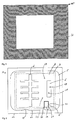
In
Auf die Seitenfläche 3 ist eine hochpräzise strukturierte spiegelnde Schicht 5 aufgebracht. Die spiegelnde Schicht 5 wird beispielsweise aus Chrom oder Wolfram hergestellt. Es können beliebige andere Materialien verwendet werden, solange durch das Substrat auf die spiegelnde Schicht (5) auftreffende Strahlung an dieser gemäß den Gesetzen der geometrischen Optik gespiegelt wird. Die spiegelnde Schicht 5 weist Aussparungen 6 auf. Auf die spiegelnde Schicht 5 und auf die Seitenfläche 3 des Substrats 2 im Bereich der Aussparungen 6 wird eine Streuschicht 7 aufgebracht. Diese ist so ausgebildet, dass sie im Auflicht auftreffende Strahlung diffus reflektiert. Bevorzugt wird Streuschicht so ausgebildet, dass die Streuschicht im Durchlicht zumindest transluzent ist, vorzugsweise diffus streut.On the
Bei der hier dargestellten Ausführungsform ist auf die Streuschicht 7 zusätzlich eine Induktionsschicht 8 aufgebracht. Diese ist aus einem Material hergestellt, welches mit einem induktiven Messsensor wechselwirkt. Insbesondere eignen sich somit metallische Materialien, die in einer ausreichenden Schichtdicke 9 aufgebracht werden. Die Induktionsschicht wird von einer Reihe von Messeinrichtungen genutzt, um eine Messung der Messeinrichtung auszulösen, wenn induktive Sensoren eine Anwesenheit der Kalibrierzelle im Erfassungsbereich der Messeinrichtung faststellen.In the embodiment illustrated here, an induction layer 8 is additionally applied to the
In
In
Schematisch ist eine solche Maske 11 in
In
Eine ebensolche Maske 11" mit einer weiteren Abdeckung 26, durch die der Randbereich 13 gemäß
In
In
Es ergibt sich für den Fachmann, dass in den schematischen Darstellungen die einzelnen Dimensionen, insbesondere die Schichtdicken des Substrats 2 im Verfiältnis zu den Schichtdicken der spiegelnden Schicht 5, der Streuschicht 7 und der Induktionsschicht 8, nicht maßstabsgerecht dargestellt sind. Die Substratschicht weist eine sehr viel größere Schichtdicke als die spiegelnde Schicht 5, die Streuschicht 7 und die Induktionsschicht 8 sowie die Antireflexschicht 16 auf.It will be apparent to those skilled in the art that in the schematic illustrations, the individual dimensions, in particular the layer thicknesses of the
Darüber hinaus ergibt sich für den Fachmann, dass die jeweilige geometrische Ausprägung der Schichten sowie die für die jeweilige Schicht gewählten Reflektionsgrade und Transmissionen abhängig vom konkret nachzubildenden Messobjekt (beispielsweise einem Erzeugnis) geeignet zu wählen sind.In addition, it results for the person skilled in the art that the respective geometric characteristics of the layers as well as the reflection levels and transmissions selected for the respective layer are to be selected as a function of the measurement object to be concretely reproduced (for example a product).
- 11
- Kalibrierzellecalibration cell
- 22
- Substratsubstratum
- 33
- Seitenflächeside surface
- 44
- gegenüberliegende Seitentlächeopposite side surface
- 55
- spiegelnde Schichtreflective layer
- 66
- Aussparungenrecesses
- 6'6 '
- Konturcontour
- 77
- Streuschichtscattering layer
- 88th
- Induktionsschichtinducing layer
- 99
- Schichtdickelayer thickness
- 1010
- Randbereichborder area
- 1111
- Maske mit einer hochpräzisen, hinsichtlich der geometrischen Abmessungen bekannten StrukturMask with a high-precision, known in terms of geometric dimensions structure
- 11'11 '
- Maske zum Aufbringen einer StreuschichtMask for applying a litter layer
- 11"11 "
- Maske zum Aufbringen einer InduktionsschichtMask for applying an induction layer
- 12, 1312, 13
- weitere Randbereichefurther border areas
- 1414
- Außenkontur des SubstratsOuter contour of the substrate
- 1515
- Außenkontur der spiegelnden SchichtOuter contour of the reflective layer
- 1616
- AntireflexionsschichtAntireflection coating
- 1717
- Konturmodifikationcontour modification
- 1818
- kleine Gebiete der spiegelnden Schichtsmall areas of the reflective layer
- 1919
- GeradeJust
- 20, 2120, 21
- PunktePoints
- 2222
- umgrenzende Konturbounding contour
- 2323
- Teileparts
- 2424
-
Abdeckung für Randbereich 10Cover for
edge area 10 - 25, 2625, 26
-
weitere Abdeckung für weitere Randbereiche 12 bzw. 13further cover for
further edge regions 12 and 13, respectively - 2727
- Löcherholes
Claims (14)
Priority Applications (1)
| Application Number | Priority Date | Filing Date | Title |
|---|---|---|---|
| EP10001391.1A EP2363684B8 (en) | 2010-02-10 | 2010-02-10 | Calibration cell |
Applications Claiming Priority (1)
| Application Number | Priority Date | Filing Date | Title |
|---|---|---|---|
| EP10001391.1A EP2363684B8 (en) | 2010-02-10 | 2010-02-10 | Calibration cell |
Publications (3)
| Publication Number | Publication Date |
|---|---|
| EP2363684A1 true EP2363684A1 (en) | 2011-09-07 |
| EP2363684B1 EP2363684B1 (en) | 2020-04-22 |
| EP2363684B8 EP2363684B8 (en) | 2020-06-10 |
Family
ID=42288576
Family Applications (1)
| Application Number | Title | Priority Date | Filing Date |
|---|---|---|---|
| EP10001391.1A Active EP2363684B8 (en) | 2010-02-10 | 2010-02-10 | Calibration cell |
Country Status (1)
| Country | Link |
|---|---|
| EP (1) | EP2363684B8 (en) |
Cited By (1)
| Publication number | Priority date | Publication date | Assignee | Title |
|---|---|---|---|---|
| US11867630B1 (en) | 2022-08-09 | 2024-01-09 | Glasstech, Inc. | Fixture and method for optical alignment in a system for measuring a surface in contoured glass sheets |
Citations (6)
| Publication number | Priority date | Publication date | Assignee | Title |
|---|---|---|---|---|
| US6664535B1 (en) * | 2002-07-16 | 2003-12-16 | Mitutoyo Corporation | Scale structures and methods usable in an absolute position transducer |
| US20040227937A1 (en) * | 1997-06-25 | 2004-11-18 | Richardson Timothy M. | Test slide for microscopes and method for the production of such a slide |
| US20060183342A1 (en) | 2005-02-15 | 2006-08-17 | Eastman Kodak Company | Metal and metal oxide patterned device |
| EP1703273A1 (en) * | 2005-03-18 | 2006-09-20 | BAM Bundesanstalt für Materialforschung und -prüfung | Multifunctional calibration device and kit and utilisation thereof for characterising luminescence measuring systems |
| JP2007328038A (en) * | 2006-06-06 | 2007-12-20 | Hitachi High-Technologies Corp | Dimension calibration sample for microscope |
| DE102008007178A1 (en) | 2008-01-30 | 2009-08-06 | Carl Zeiss Microimaging Gmbh | Calibration device and laser scanning microscope with such a calibration device |
-
2010
- 2010-02-10 EP EP10001391.1A patent/EP2363684B8/en active Active
Patent Citations (6)
| Publication number | Priority date | Publication date | Assignee | Title |
|---|---|---|---|---|
| US20040227937A1 (en) * | 1997-06-25 | 2004-11-18 | Richardson Timothy M. | Test slide for microscopes and method for the production of such a slide |
| US6664535B1 (en) * | 2002-07-16 | 2003-12-16 | Mitutoyo Corporation | Scale structures and methods usable in an absolute position transducer |
| US20060183342A1 (en) | 2005-02-15 | 2006-08-17 | Eastman Kodak Company | Metal and metal oxide patterned device |
| EP1703273A1 (en) * | 2005-03-18 | 2006-09-20 | BAM Bundesanstalt für Materialforschung und -prüfung | Multifunctional calibration device and kit and utilisation thereof for characterising luminescence measuring systems |
| JP2007328038A (en) * | 2006-06-06 | 2007-12-20 | Hitachi High-Technologies Corp | Dimension calibration sample for microscope |
| DE102008007178A1 (en) | 2008-01-30 | 2009-08-06 | Carl Zeiss Microimaging Gmbh | Calibration device and laser scanning microscope with such a calibration device |
Cited By (1)
| Publication number | Priority date | Publication date | Assignee | Title |
|---|---|---|---|---|
| US11867630B1 (en) | 2022-08-09 | 2024-01-09 | Glasstech, Inc. | Fixture and method for optical alignment in a system for measuring a surface in contoured glass sheets |
Also Published As
| Publication number | Publication date |
|---|---|
| EP2363684B8 (en) | 2020-06-10 |
| EP2363684B1 (en) | 2020-04-22 |
Similar Documents
| Publication | Publication Date | Title |
|---|---|---|
| DE102009040642B3 (en) | Method and device for measuring optical characteristics of transparent, scattering measuring objects | |
| DE102005030753B4 (en) | Optical strain gauge | |
| EP0175142A2 (en) | Ellipsometric device for the examination of physical surface properties of a sample | |
| EP0201861B1 (en) | Optical tension-measuring process and device | |
| DE102011050969A1 (en) | Apparatus for referenced measurement of reflected light and method for calibrating such a device | |
| DE10153147A1 (en) | Method of applying a scale to a support | |
| DE102010037207B3 (en) | Device for measuring surface roughness of material surface of planar measuring object i.e. mirror, in e.g. semiconductor industry, has determining unit for determining surface roughness based on interference fringe contrasts | |
| EP1262735A1 (en) | Method for the absolute calibration of an interferometer | |
| EP2363684B1 (en) | Calibration cell | |
| DE102019114167A1 (en) | Optical measuring device and method | |
| WO2024056501A1 (en) | Method for processing a reference element for an interferometer | |
| DE102017113897A1 (en) | Calibration standard and method for its production | |
| DE202023100328U1 (en) | A device for measuring blood plasma based on Tamm plasmon polariton | |
| DE202010002185U1 (en) | calibration cell | |
| EP2028480B1 (en) | Method and device for inspecting a test object | |
| DE10224317A1 (en) | Procedure for the calibration of a radius test station | |
| DE3120653C2 (en) | Device for determining movement quantities or creep conditions on materials | |
| EP1602919B1 (en) | Measuring device for the survey of the transmittance of a coating | |
| DE2417232A1 (en) | Non-destructive fatigue measurement in components - by observation of surface structure involves indicator layer on surface | |
| WO2005022127A2 (en) | Device for measuring a planar element | |
| DE102021125813B4 (en) | Double-mirror shear interferometer and method for non-destructive measurement of a surface using interferometric measuring methods | |
| DE102011087978A1 (en) | Method and device for determining the refractive index gradient of a material | |
| DE102008021072B4 (en) | Method for measuring edge or edge stresses in glass panes | |
| DE102005054552B4 (en) | Apparatus and method for testing semiconductor substrates for cracks | |
| LU100683B1 (en) | Test method for determining the climatic resistance of a coating for a substrate and device therefor |
Legal Events
| Date | Code | Title | Description |
|---|---|---|---|
| PUAI | Public reference made under article 153(3) epc to a published international application that has entered the european phase |
Free format text: ORIGINAL CODE: 0009012 |
|
| AK | Designated contracting states |
Kind code of ref document: A1 Designated state(s): AT BE BG CH CY CZ DE DK EE ES FI FR GB GR HR HU IE IS IT LI LT LU LV MC MK MT NL NO PL PT RO SE SI SK SM TR |
|
| AX | Request for extension of the european patent |
Extension state: AL BA RS |
|
| 17P | Request for examination filed |
Effective date: 20120307 |
|
| 17Q | First examination report despatched |
Effective date: 20120810 |
|
| STAA | Information on the status of an ep patent application or granted ep patent |
Free format text: STATUS: EXAMINATION IS IN PROGRESS |
|
| REG | Reference to a national code |
Ref country code: DE Ref legal event code: R079 Ref document number: 502010016590 Country of ref document: DE Free format text: PREVIOUS MAIN CLASS: G01B0003300000 Ipc: G01N0021270000 |
|
| GRAP | Despatch of communication of intention to grant a patent |
Free format text: ORIGINAL CODE: EPIDOSNIGR1 |
|
| STAA | Information on the status of an ep patent application or granted ep patent |
Free format text: STATUS: GRANT OF PATENT IS INTENDED |
|
| RIC1 | Information provided on ipc code assigned before grant |
Ipc: G01N 21/27 20060101AFI20190924BHEP |
|
| INTG | Intention to grant announced |
Effective date: 20191017 |
|
| GRAS | Grant fee paid |
Free format text: ORIGINAL CODE: EPIDOSNIGR3 |
|
| GRAJ | Information related to disapproval of communication of intention to grant by the applicant or resumption of examination proceedings by the epo deleted |
Free format text: ORIGINAL CODE: EPIDOSDIGR1 |
|
| GRAL | Information related to payment of fee for publishing/printing deleted |
Free format text: ORIGINAL CODE: EPIDOSDIGR3 |
|
| STAA | Information on the status of an ep patent application or granted ep patent |
Free format text: STATUS: EXAMINATION IS IN PROGRESS |
|
| GRAR | Information related to intention to grant a patent recorded |
Free format text: ORIGINAL CODE: EPIDOSNIGR71 |
|
| STAA | Information on the status of an ep patent application or granted ep patent |
Free format text: STATUS: GRANT OF PATENT IS INTENDED |
|
| GRAA | (expected) grant |
Free format text: ORIGINAL CODE: 0009210 |
|
| STAA | Information on the status of an ep patent application or granted ep patent |
Free format text: STATUS: THE PATENT HAS BEEN GRANTED |
|
| INTC | Intention to grant announced (deleted) | ||
| AK | Designated contracting states |
Kind code of ref document: B1 Designated state(s): AT BE BG CH CY CZ DE DK EE ES FI FR GB GR HR HU IE IS IT LI LT LU LV MC MK MT NL NO PL PT RO SE SI SK SM TR |
|
| INTG | Intention to grant announced |
Effective date: 20200313 |
|
| REG | Reference to a national code |
Ref country code: GB Ref legal event code: FG4D Free format text: NOT ENGLISH |
|
| REG | Reference to a national code |
Ref country code: CH Ref legal event code: EP |
|
| REG | Reference to a national code |
Ref country code: DE Ref legal event code: R096 Ref document number: 502010016590 Country of ref document: DE |
|
| RAP2 | Party data changed (patent owner data changed or rights of a patent transferred) |
Owner name: ISRA VISION GRAPHIKON GMBH |
|
| REG | Reference to a national code |
Ref country code: IE Ref legal event code: FG4D Free format text: LANGUAGE OF EP DOCUMENT: GERMAN |
|
| REG | Reference to a national code |
Ref country code: AT Ref legal event code: REF Ref document number: 1260777 Country of ref document: AT Kind code of ref document: T Effective date: 20200515 Ref country code: CH Ref legal event code: PK Free format text: BERICHTIGUNG B8 |
|
| REG | Reference to a national code |
Ref country code: LT Ref legal event code: MG4D |
|
| REG | Reference to a national code |
Ref country code: NL Ref legal event code: MP Effective date: 20200422 |
|
| PG25 | Lapsed in a contracting state [announced via postgrant information from national office to epo] |
Ref country code: FI Free format text: LAPSE BECAUSE OF FAILURE TO SUBMIT A TRANSLATION OF THE DESCRIPTION OR TO PAY THE FEE WITHIN THE PRESCRIBED TIME-LIMIT Effective date: 20200422 Ref country code: PT Free format text: LAPSE BECAUSE OF FAILURE TO SUBMIT A TRANSLATION OF THE DESCRIPTION OR TO PAY THE FEE WITHIN THE PRESCRIBED TIME-LIMIT Effective date: 20200824 Ref country code: SE Free format text: LAPSE BECAUSE OF FAILURE TO SUBMIT A TRANSLATION OF THE DESCRIPTION OR TO PAY THE FEE WITHIN THE PRESCRIBED TIME-LIMIT Effective date: 20200422 Ref country code: NL Free format text: LAPSE BECAUSE OF FAILURE TO SUBMIT A TRANSLATION OF THE DESCRIPTION OR TO PAY THE FEE WITHIN THE PRESCRIBED TIME-LIMIT Effective date: 20200422 Ref country code: LT Free format text: LAPSE BECAUSE OF FAILURE TO SUBMIT A TRANSLATION OF THE DESCRIPTION OR TO PAY THE FEE WITHIN THE PRESCRIBED TIME-LIMIT Effective date: 20200422 Ref country code: GR Free format text: LAPSE BECAUSE OF FAILURE TO SUBMIT A TRANSLATION OF THE DESCRIPTION OR TO PAY THE FEE WITHIN THE PRESCRIBED TIME-LIMIT Effective date: 20200723 Ref country code: NO Free format text: LAPSE BECAUSE OF FAILURE TO SUBMIT A TRANSLATION OF THE DESCRIPTION OR TO PAY THE FEE WITHIN THE PRESCRIBED TIME-LIMIT Effective date: 20200722 Ref country code: IS Free format text: LAPSE BECAUSE OF FAILURE TO SUBMIT A TRANSLATION OF THE DESCRIPTION OR TO PAY THE FEE WITHIN THE PRESCRIBED TIME-LIMIT Effective date: 20200822 |
|
| PG25 | Lapsed in a contracting state [announced via postgrant information from national office to epo] |
Ref country code: LV Free format text: LAPSE BECAUSE OF FAILURE TO SUBMIT A TRANSLATION OF THE DESCRIPTION OR TO PAY THE FEE WITHIN THE PRESCRIBED TIME-LIMIT Effective date: 20200422 Ref country code: HR Free format text: LAPSE BECAUSE OF FAILURE TO SUBMIT A TRANSLATION OF THE DESCRIPTION OR TO PAY THE FEE WITHIN THE PRESCRIBED TIME-LIMIT Effective date: 20200422 Ref country code: BG Free format text: LAPSE BECAUSE OF FAILURE TO SUBMIT A TRANSLATION OF THE DESCRIPTION OR TO PAY THE FEE WITHIN THE PRESCRIBED TIME-LIMIT Effective date: 20200722 |
|
| REG | Reference to a national code |
Ref country code: DE Ref legal event code: R097 Ref document number: 502010016590 Country of ref document: DE |
|
| PG25 | Lapsed in a contracting state [announced via postgrant information from national office to epo] |
Ref country code: EE Free format text: LAPSE BECAUSE OF FAILURE TO SUBMIT A TRANSLATION OF THE DESCRIPTION OR TO PAY THE FEE WITHIN THE PRESCRIBED TIME-LIMIT Effective date: 20200422 Ref country code: IT Free format text: LAPSE BECAUSE OF FAILURE TO SUBMIT A TRANSLATION OF THE DESCRIPTION OR TO PAY THE FEE WITHIN THE PRESCRIBED TIME-LIMIT Effective date: 20200422 Ref country code: SM Free format text: LAPSE BECAUSE OF FAILURE TO SUBMIT A TRANSLATION OF THE DESCRIPTION OR TO PAY THE FEE WITHIN THE PRESCRIBED TIME-LIMIT Effective date: 20200422 Ref country code: CZ Free format text: LAPSE BECAUSE OF FAILURE TO SUBMIT A TRANSLATION OF THE DESCRIPTION OR TO PAY THE FEE WITHIN THE PRESCRIBED TIME-LIMIT Effective date: 20200422 Ref country code: RO Free format text: LAPSE BECAUSE OF FAILURE TO SUBMIT A TRANSLATION OF THE DESCRIPTION OR TO PAY THE FEE WITHIN THE PRESCRIBED TIME-LIMIT Effective date: 20200422 Ref country code: ES Free format text: LAPSE BECAUSE OF FAILURE TO SUBMIT A TRANSLATION OF THE DESCRIPTION OR TO PAY THE FEE WITHIN THE PRESCRIBED TIME-LIMIT Effective date: 20200422 Ref country code: DK Free format text: LAPSE BECAUSE OF FAILURE TO SUBMIT A TRANSLATION OF THE DESCRIPTION OR TO PAY THE FEE WITHIN THE PRESCRIBED TIME-LIMIT Effective date: 20200422 |
|
| PG25 | Lapsed in a contracting state [announced via postgrant information from national office to epo] |
Ref country code: PL Free format text: LAPSE BECAUSE OF FAILURE TO SUBMIT A TRANSLATION OF THE DESCRIPTION OR TO PAY THE FEE WITHIN THE PRESCRIBED TIME-LIMIT Effective date: 20200422 Ref country code: SK Free format text: LAPSE BECAUSE OF FAILURE TO SUBMIT A TRANSLATION OF THE DESCRIPTION OR TO PAY THE FEE WITHIN THE PRESCRIBED TIME-LIMIT Effective date: 20200422 |
|
| PLBE | No opposition filed within time limit |
Free format text: ORIGINAL CODE: 0009261 |
|
| STAA | Information on the status of an ep patent application or granted ep patent |
Free format text: STATUS: NO OPPOSITION FILED WITHIN TIME LIMIT |
|
| 26N | No opposition filed |
Effective date: 20210125 |
|
| PG25 | Lapsed in a contracting state [announced via postgrant information from national office to epo] |
Ref country code: SI Free format text: LAPSE BECAUSE OF FAILURE TO SUBMIT A TRANSLATION OF THE DESCRIPTION OR TO PAY THE FEE WITHIN THE PRESCRIBED TIME-LIMIT Effective date: 20200422 |
|
| PG25 | Lapsed in a contracting state [announced via postgrant information from national office to epo] |
Ref country code: MC Free format text: LAPSE BECAUSE OF FAILURE TO SUBMIT A TRANSLATION OF THE DESCRIPTION OR TO PAY THE FEE WITHIN THE PRESCRIBED TIME-LIMIT Effective date: 20200422 |
|
| REG | Reference to a national code |
Ref country code: BE Ref legal event code: MM Effective date: 20210228 |
|
| PG25 | Lapsed in a contracting state [announced via postgrant information from national office to epo] |
Ref country code: LU Free format text: LAPSE BECAUSE OF NON-PAYMENT OF DUE FEES Effective date: 20210210 Ref country code: LI Free format text: LAPSE BECAUSE OF NON-PAYMENT OF DUE FEES Effective date: 20210228 Ref country code: CH Free format text: LAPSE BECAUSE OF NON-PAYMENT OF DUE FEES Effective date: 20210228 |
|
| PG25 | Lapsed in a contracting state [announced via postgrant information from national office to epo] |
Ref country code: IE Free format text: LAPSE BECAUSE OF NON-PAYMENT OF DUE FEES Effective date: 20210210 |
|
| REG | Reference to a national code |
Ref country code: AT Ref legal event code: MM01 Ref document number: 1260777 Country of ref document: AT Kind code of ref document: T Effective date: 20210210 |
|
| PG25 | Lapsed in a contracting state [announced via postgrant information from national office to epo] |
Ref country code: AT Free format text: LAPSE BECAUSE OF NON-PAYMENT OF DUE FEES Effective date: 20210210 |
|
| PG25 | Lapsed in a contracting state [announced via postgrant information from national office to epo] |
Ref country code: BE Free format text: LAPSE BECAUSE OF NON-PAYMENT OF DUE FEES Effective date: 20210228 |
|
| PGFP | Annual fee paid to national office [announced via postgrant information from national office to epo] |
Ref country code: FR Payment date: 20230221 Year of fee payment: 14 |
|
| PG25 | Lapsed in a contracting state [announced via postgrant information from national office to epo] |
Ref country code: HU Free format text: LAPSE BECAUSE OF FAILURE TO SUBMIT A TRANSLATION OF THE DESCRIPTION OR TO PAY THE FEE WITHIN THE PRESCRIBED TIME-LIMIT; INVALID AB INITIO Effective date: 20100210 Ref country code: CY Free format text: LAPSE BECAUSE OF FAILURE TO SUBMIT A TRANSLATION OF THE DESCRIPTION OR TO PAY THE FEE WITHIN THE PRESCRIBED TIME-LIMIT Effective date: 20200422 |
|
| PGFP | Annual fee paid to national office [announced via postgrant information from national office to epo] |
Ref country code: GB Payment date: 20230220 Year of fee payment: 14 Ref country code: DE Payment date: 20230216 Year of fee payment: 14 |