EP2362641B1 - Abbildungssystem - Google Patents
Abbildungssystem Download PDFInfo
- Publication number
- EP2362641B1 EP2362641B1 EP11154913.5A EP11154913A EP2362641B1 EP 2362641 B1 EP2362641 B1 EP 2362641B1 EP 11154913 A EP11154913 A EP 11154913A EP 2362641 B1 EP2362641 B1 EP 2362641B1
- Authority
- EP
- European Patent Office
- Prior art keywords
- peripheral
- region
- frame
- array
- subset
- Prior art date
- Legal status (The legal status is an assumption and is not a legal conclusion. Google has not performed a legal analysis and makes no representation as to the accuracy of the status listed.)
- Active
Links
Images

Classifications
-
- H—ELECTRICITY
- H04—ELECTRIC COMMUNICATION TECHNIQUE
- H04N—PICTORIAL COMMUNICATION, e.g. TELEVISION
- H04N25/00—Circuitry of solid-state image sensors [SSIS]; Control thereof
- H04N25/40—Extracting pixel data from image sensors by controlling scanning circuits, e.g. by modifying the number of pixels sampled or to be sampled
- H04N25/44—Extracting pixel data from image sensors by controlling scanning circuits, e.g. by modifying the number of pixels sampled or to be sampled by partially reading an SSIS array
- H04N25/445—Extracting pixel data from image sensors by controlling scanning circuits, e.g. by modifying the number of pixels sampled or to be sampled by partially reading an SSIS array by skipping some contiguous pixels within the read portion of the array
-
- H—ELECTRICITY
- H04—ELECTRIC COMMUNICATION TECHNIQUE
- H04N—PICTORIAL COMMUNICATION, e.g. TELEVISION
- H04N23/00—Cameras or camera modules comprising electronic image sensors; Control thereof
- H04N23/20—Cameras or camera modules comprising electronic image sensors; Control thereof for generating image signals from infrared radiation only
- H04N23/23—Cameras or camera modules comprising electronic image sensors; Control thereof for generating image signals from infrared radiation only from thermal infrared radiation
Definitions
- An imaging system may have a detector that generates a signal in response to detecting light from a scene, a processor that processes the signal, and a display that displays an image of the scene using the processed signal.
- signal processing may increase the size, weight, computational, and/or power burden. Accordingly, in certain situations, processing may be reduced to decrease these burdens.
- Published US patent application no 2002/0105584 discloses a device and method for reading out the image points of a 2D electronic image sensor, an image thereon being divided into regions of greater and lesser interest, the region of greater interest being read out at a scanning rate which is higher than that used for the region of lesser interest. The region of greater interest can therefore be reproduced with a higher temporal resolution whilst making optimum use of limited processing resources.
- Published US patent application no 2004/0069492 discloses a variable acuity imager incorporating an array of light detection elements and means for changing the effective spatial configuration of the array to include "superpixels" by combining the energy detected by adjacent pixels. Any number of high-resolution foveal regions can be arranged within the array and moved around at the frame rate of the imaging device.
- Document US2009/167920 A1 discloses an image sensor which generates successive frames from spatially different pixel groups of the sensor at high frame rate.
- the frame rate of the imaging element can be kept high while a high display resolution is maintained.
- the present invention provides a method according to claim 1, and a system according to claim 11.
- Certain embodiments of the invention may provide one or more technical advantages.
- a technical advantage of one embodiment may be that processing data for a peripheral region may be reduced relative to processing data for a foveal region, which may reduce burdens on the imaging system.
- Another technical advantage of one embodiment may be that the foveal region can be adjusted.
- FIGURES 1 through 3 of the drawings like numerals being used for like and corresponding parts of the various drawings.
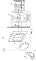
- FIGURE 1 illustrates an example of an imaging system 10 that may be used to generate an image 50 of a scene 12.
- scene 12 includes objects 14.
- System 10 includes a camera 18, a computing system 20, and a display 22 coupled as shown.
- Camera 18 includes optics 24, a focal plane array (or detector array) 26, and integrated circuit 28.
- Focal plane array 26 includes a focal region 52 and a peripheral region 54.
- Computing system 20 includes an interface 32, logic 34, and a memory 36.
- Logic 34 includes one or more processors 40 and applications such as an image processor 44.
- Memory 36 stores applications.
- Display 22 displays image 50 of scene 12.
- Display 22 has a foveal region 62 and a peripheral region 64.
- system 10 may sample foveal array elements of foveal region 52 of focal plane array 26 at a faster sampling rate to yield foveal array data.
- System 10 may sample peripheral array elements of peripheral region 54 of focal plane array at a slower sampling rate to yield peripheral array data.
- System 10 may process the foveal array data to yield foveal image data for foveal region 62 of display 22, and may process the peripheral array data to yield peripheral image data for peripheral region 64 of display 22.
- scene 12 includes objects 14 that reflect and/or emit light that may be used to generate image 50 of scene 12.
- Camera 18 receives light from scene 12.
- Optics 24 refracts or reflects the light to direct the light towards focal plane array 26.
- Optics 24 may comprise one or more optical devices such as lenses.
- Focal plane array 26 may comprise an array (such as a two-dimensional array) of detector elements that can detect light and generate detector signals in response to the detected light.
- the detector signal corresponding to a detector element includes array data that represents the amount and/or wavelength of light that is detected by the detector element.
- Examples of focal plane arrays include complementary metal-oxide-semiconductor (CMOS) imagers, charge coupled devices, hybrid infrared imagers, and uncooled microbolometers.
- CMOS complementary metal-oxide-semiconductor
- focal plane array 26 may have foveal region 52 that comprises foveal array elements and peripheral region 54 that comprises peripheral array elements.
- Focal plane array 26 may generate array data (which may also be referred to as focal plane array, focal plane, or detector data).
- the focal plane array's foveal region 52 may generate foveal data (such as foveal array data), which may be used to generate foveal region 62 of display 22 (display foveal region).
- the focal plane array's peripheral region 54 may generate peripheral data (such as peripheral array data), which may be used to generate peripheral region 64 of display 22 (or display peripheral region).
- Foveal regions 52 and 62 may have any suitable size and shape, and may comprise any portion of array 26 and display 22, respectively.
- a foveal region 52 and/or 62 corresponds to the foveal portion of an eye's field-of-view, which detects visual information with greater precision than the peripheral region of the field-of-view.
- foveal regions 52 and 62 may be located near or at the central portion of array 26 and display 22, respectively, and the peripheral regions 54 and 64 may surround the foveal regions 52 and 62, respectively.
- the size and position of foveal regions 52 and 62 and/or peripheral regions 54 and 64 may be changed.
- a foveal region 52 or 62 may be moved from the center to the upper left corner.
- foveal region 52 or 62 may be made smaller or larger.
- the size and position of a foveal region 52 or 62 may be determined according to image 50.
- image 50 may include an element of interest that moves, and foveal region 52 or 62 may move where the element moves.
- Integrated circuit 28 controls operation of and/or processes signals from focal plane array 26.
- integrated circuit 28 reads and outputs the detector signals.
- An example of integrated circuit 28 is a read-out integrated circuit (RoIC) 28.
- Integrated circuit 28 may output the signals according to any suitable protocol, such as the National Television System Committee (NTSC) protocol, Phase Alternating Line (PAL) protocol, or sequential color with memory (SECAM) protocol.
- NTSC National Television System Committee
- PAL Phase Alternating Line
- SECAM sequential color with memory
- Integrated circuit 28 may include several components that control operation of and/or processes signals from focal plane array 26.
- integrated circuit 28 includes power circuitry that controls power to array 26, timing circuitry that provides clock signals, synchronization circuitry that synchronizes the timing of array 26, amplifying circuitry that amplifies signals from array 26, filter circuitry that filters signals from array 26, and/or an analog-to-digital (A/D) circuitry that digitizes video signals generated by array 26.
- power circuitry that controls power to array 26
- timing circuitry that provides clock signals
- synchronization circuitry that synchronizes the timing of array 26
- amplifying circuitry that amplifies signals from array 26
- filter circuitry that filters signals from array 26
- A/D analog-to-digital
- Computing system 20 facilitates the operation of and/or processes signals of system 10.
- image processor 44 processes array data from camera 12 to yield image data used to display image 50 on display 22.
- Image data for a pixel of image 50 may indicate the amount and/or wavelength of light detected by a detector element that corresponds to the pixel.
- a scan of substantially all of focal plane array 26 may yield a frame of data.
- a frame of focal plane data may be used to generate a frame of image data used to display image 50 at a particular time. Frames may be generated at successive times to yield a moving image 50 of scene 12.
- image processor 44 may perform other suitable operations.
- image processor 44 may perform a sharpening operation on focal plane data to sharpen image 50.
- image processor 44 may perform an image recognition operation that detects certain features, such as colors or outlines.
- Display 50 may be any suitable device configured to display image 50 of scene 12 using image data.
- display 50 comprises display foveal region 62 and display peripheral region 64.
- Display foveal region 62 generates a portion of image 50 from foveal image data, which is in turn generated from foveal focal plane data from focal plane's foveal region 52.
- Display peripheral region 64 generates a portion of image 50 from peripheral image data, which is in turn generated from peripheral array data from detector peripheral region 54.
- Display 22 may be any suitable size and/or shape.
- the reduced processing may allow for applications in devices with size and/or weight restrictions and/or limited computational and/or power resources.
- display 50 is sufficiently small to be placed in close proximity (such as less than 1, 1 to 2, or 2 to 5 inches) to a human eye such that image 50 fits within the vision of the eye.
- Examples of such displays 50 include head mounted displays (HMDs) and displays for eyepieces of optical devices, such as binoculars or telescopes. Head mounted displays are devices that may be worn by a user and include a relatively small computer display that is positioned in front of the user's eyes.
- focal plane array 26 may selectively scan certain detector elements and not scan other regions.
- a controller (such as drive circuit 28 and/or image processor 44) may instruct focal plane array 26 to scan the detector elements.
- a smaller percentage of focal plane array peripheral region 54 may be sampled in a unit of time, and a larger percentage of focal plane array foveal region 52 may be sampled in the unit of time.
- the data processing of system 10 may be less than that of a system that samples the higher percentage for both focal plane array peripheral region 54 and focal plane array foveal region 52.
- foveal array elements may be sampled at a faster sampling rate to yield foveal array data
- peripheral array elements may be sampled at a slower sampling rate to yield peripheral focal plane array data.
- the sampling rate may represent the number of elements sampled per unit time. Examples of a faster sampling rate include a rate in the ranges of 10 to 20, 20 to 30, and 30 or more frames per second.
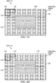
- FIGURES 2A through 2D illustrate an example of a method for sampling focal plane array 26 that may be used with system 10 of FIGURE 1 .
- Array 26 includes foveal region 126 comprising foveal array elements and peripheral region 128 comprising peripheral array elements 130.
- peripheral array elements 130 are organized into sub-regions 132.
- Each sub-region 132 may comprise two or more peripheral array elements 130, and may comprise any suitable shape.
- sub-region 132 may comprise m ⁇ n peripheral array elements 130, and may be a m ⁇ n rectangle, where m represents the number of rows and n represents the number of columns of elements 130.
- Each sub-region 132 may comprise two or more subsets 140.
- Each subset 140 may include one or more peripheral array elements 130 that are sampled for a frame.
- a first subset 140 is sampled for a first frame
- a second subset 140 is sampled for a second frame.
- a sub-region 132 has four peripheral array elements 130 arranged in a 2 ⁇ 2 rectangle.
- Sub-region 132 has four subsets 140, where each subset 140 includes one peripheral array element 130
- Foveal region 126 may be scanned at a faster scanning rate, while peripheral region 128 may be scanned at a slower scanning rate.
- a proper subset of each sub-region 132 of peripheral region 128 may be scanned for a frame.
- a proper subset of set S is a subset that is strictly contained in S and so excludes at least one member of S. That is, not all elements of sub-region 132 are scanned at each frame.
- different elements of a sub-region 132 may be scanned for different frames. For example, a first subset of the sub-region 132 may be sampled for a first frame, and a second subset of the sub-region 132 may be sampled for a second frame, where the second subset not equal to the first subset. Two sets are not equal if they do not have the same elements. Unequal sets may have at least one common element or may have no common elements.
- FIGURES 2A through 2D illustrate scanning for four frames. Substantially all of foveal region 126 is scanned for each frame. Different subsets 140 of peripheral region 128 are scanned for different frames. For example, subset 140 of the upper left corner of each sub-region 132 may be scanned for a first frame as shown in FIGURE 2A . Subset 140 of the lower right corner of each sub-region 132 may be scanned for a second frame as shown in FIGURE 2B . Subset 140 of the upper right corner of each sub-region 132 may be scanned for a third frame as shown in FIGURE 2C . Subset 140 of the lower left corner of each sub-region 132 may be scanned for a fourth frame as shown in FIGURE 2D . In the example, sub-regions 132 are processed with a 75 percent reduction in processing load.
- the scanning may be adjusted in any suitable manner. For example, if power is running low, the sampling rate may be decreased, or if power is increased, the sampling rate may be increased. As another example, a user may request a faster or slower scanning rate. As another example, system 10 may detect increased motion of scene 12 and may increase the sampling rate, or may detect decreased motion of scene 12 and may decrease the sampling rate.
- Image processor 44 may process the array data in any suitable manner to generate image 50.
- image processor 44 may process peripheral array data from a first subset 140 to yield first image data for a first frame.
- the first subset 140 is not sampled for the next frame, so the first image data is utilized for the next frame.
- the first image data may be utilized in any suitable manner.
- the first image data may be held for the next frame.
- the first image data may be averaged with second image data generated using a second subset 140, and the averaged data may be used for the next frame.
- image processor 44 may use first image data generated using a first subset 140 for a first frame and a second frame, and may use second image data using a second subset 140 for a second frame and a third frame.
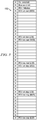
- FIGURE 3 illustrates an example of a messaging sequence 150 that may be used to set the size of a foveal region of a focal plane array 26.
- Messaging sequence 150 may be used to communicate among the components of system 10, such as among camera 18, computing system 20, and/or display 22.
- messaging sequence 150 may be used to communicate array data from camera 12 to display 22, camera settings or scanning instructions from computing system 20 to camera 18, or instructions for displaying image to image processor 44 or display 22.
- messaging sequence 150 may be used to instruct integrated circuit 28 to set or change the size of the detector foveal region.
- Messaging sequence 150 indicates the array elements that are designated as foveal array elements.
- messaging sequence 150 includes fovea start addresses and fovea stop addresses.
- a fovea start address may be a row start address that indicates the start of a row of the foveal region, or may be a column start address that indicates the start of a column of the foveal region, or a combination of both the row and column starting address.
- a fovea stop address may be a row stop address that indicates the end of a row of the foveal region, or may be a column stop address that indicates the end of a column of the foveal region, or a combination of both the row and column ending address.
- messaging sequence 150 may be used to instruct integrated circuit 28 to set or change the size of the detector peripheral region.
- a focal plane may be an array of microbolometers.
- provisions may be made to accommodate changes in microbolometer Joule heating as the sampling rate is varied relative to the foveal region. For example, a constant bias duty cycle may be maintained on the microbolometer as the sampling rate is changed. As another example, changes in the bolometer's resistance due to Joule heating may be compensated for by electronically adjusting the microbolometer's bias conditions or the operating bias in supporting circuitry.
- a component of the systems and apparatuses disclosed herein may include an interface, logic, memory, and/or other suitable element.
- An interface receives input, sends output, processes the input and/or output, and/or performs other suitable operation.
- An interface may comprise hardware and/or software.
- Logic performs the operations of the component, for example, executes instructions to generate output from input.
- Logic may include hardware, software, and/or other logic.
- Logic may be encoded in one or more tangible media and may perform operations when executed by a computer.
- Certain logic, such as a processor may manage the operation of a component. Examples of a processor include one or more computers, one or more microprocessors, one or more field programmable gate arrays, one or more digital signal processors, one or more applications, and/or other logic.
- the operations of the embodiments may be performed by one or more computer readable media encoded with a computer program, software, computer executable instructions, and/or instructions capable of being executed by a computer.
- the operations of the embodiments may be performed by one or more field programmable gate arrays configured by firmware to implement logical functions.
- the operations of the embodiments may be performed by one or more computer readable media storing, embodied with, and/or encoded with a computer program and/or having a stored and/or an encoded computer program.
- a memory stores information.
- a memory may comprise one or more non-transitory, tangible, computer-readable, and/or computer-executable storage media. Examples of memory include computer memory (for example, Random Access Memory (RAM) or Read Only Memory (ROM)), mass storage media (for example, a hard disk), removable storage media (for example, a Compact Disk (CD) or a Digital Video Disk (DVD)), database and/or network storage (for example, a server), and/or other computer-readable medium.
- RAM Random Access Memory
- ROM Read Only Memory
- mass storage media for example, a hard disk
- removable storage media for example, a Compact Disk (CD) or a Digital Video Disk (DVD)
- database and/or network storage for example, a server
- network storage for example, a server
Landscapes
- Engineering & Computer Science (AREA)
- Multimedia (AREA)
- Signal Processing (AREA)
- Health & Medical Sciences (AREA)
- Toxicology (AREA)
- Studio Devices (AREA)
Claims (18)
- Verfahren zum Erzeugen von Infrarotbildern, umfassend:für jedes einer Vielzahl von Einzelbildern Abtasten einer Vielzahl von Elementen einer fovealen Anordnung, die einen fovealen Detektorbereich einer Mikrobolometeranordnung mit einer schnelleren Abtastrate bildet, um Daten der fovealen Anordnung zu ergeben;Abtasten einer Vielzahl von Elementen einer peripheren Anordnung, die einen peripheren Detektorbereich der Mikrobolometeranordnung mit einer langsameren Abtastrate bildet, um Daten der peripheren Anordnung zu ergeben, wobei die Vielzahl der Elemente der peripheren Anordnung eine Vielzahl von Teilbereichen umfasst, wobei jeder Teilbereich zwei oder mehrere Elemente der peripheren Anordnung umfasst, wobei das Abtasten der Vielzahl der Elemente der peripheren Anordnung ferner für jeden Teilbereich Folgendes umfasst:Abtasten eines ersten Teilsatzes jedes Teilbereichs für ein erstes Einzelbild der Vielzahl von Einzelbildern; undAbtasten eines zweiten Teilsatzes jedes Teilbereichs für ein zweites Einzelbild der Vielzahl von Einzelbildern, wobei der zweite Teilsatz nicht gleich dem ersten Teilsatz ist;Verarbeiten der Daten der fovealen Anordnung, um foveale Bilddaten für einen fovealen Anzeigebereich einer Anzeige zu ergeben; undVerarbeiten der Daten der peripheren Anordnung, um periphere Bilddaten für einen peripheren Anzeigebereich der Anzeige zu ergeben.
- Verfahren nach Anspruch 1, wobei der erste und der zweite Teilsatz ordnungsgemäße Teilsätze jedes Teilbereichs sind.
- Verfahren nach Anspruch 1 oder Verfahren nach Anspruch 2, wobei das Verarbeiten der Daten der peripheren Anordnung ferner Folgendes umfasst:Erzeugen erster Bilddaten, die aus dem ersten Teilsatz der Elemente der peripheren Anordnung erzeugt werden, für das erste Einzelbild und das zweite Einzelbild; undErzeugen zweiter Bilddaten, die aus dem zweiten Teilsatz der Elemente der peripheren Anordnung erzeugt werden, für das zweite Einzelbild und ein drittes Einzelbild.
- Verfahren nach einem vorhergehenden Anspruch, wobei das Verarbeiten der Daten der peripheren Anordnung ferner Folgendes umfasst:Erzeugen erster Bilddaten, die aus dem ersten Teilsatz der Elemente der peripheren Anordnung erzeugt werden, für das erste Einzelbild; undHalten der ersten Bilddaten für das zweite Einzelbild.
- Verfahren nach einem vorhergehenden Anspruch, wobei das Verarbeiten der Daten der peripheren Anordnung ferner Folgendes umfasst:Erzeugen der ersten Bilddaten, die aus dem ersten Teilsatz der Elemente der peripheren Anordnung erzeugt werden, für das erste Einzelbild; undMitteln der ersten Bilddaten mit den zweiten Bilddaten, die aus einem zweiten Teilsatz der Elemente der peripheren Anordnung erzeugt werden, für das zweite Einzelbild.
- Verfahren nach einem vorhergehenden Anspruch, ferner umfassend:Bezeichnen einer Vielzahl von Anordnungselementen als Elemente der fovealen Anordnung, um den fovealen Bereich einzustellen.
- Verfahren nach einem vorhergehenden Anspruch, ferner umfassend das Einstellen des fovealen Bereichs durch:Senden einer oder mehrerer Fovea-Startadressen und einer oder mehrerer Fovea-Stoppadressen an die Mikrobolometeranordnung.
- Verfahren nach einem vorhergehenden Anspruch:ferner umfassend das Aufrechterhalten eines konstanten vorgespannten Arbeitszyklus, während sich ein Abtastarbeitszyklus ändert.
- Verfahren nach einem der Ansprüche 1 bis 7:ferner umfassend das elektronische Einstellen einer oder mehrerer Vorspannungsbedingungen des Mikrobolometers, um eine Auswirkung einer oder mehrerer Änderungen der Jouleschen Erwärmung in einem oder mehreren Elementen der peripheren Anordnung bei der Änderung eines Abtastarbeitszyklus zu kompensieren.
- Verfahren nach einem der Ansprüche 1 bis 7:ferner umfassend das elektronische Einstellen einer Betriebsvorspannung der Unterstützungsschaltung des Mikrobolometers, um eine Auswirkung einer oder mehrerer Änderungen der Jouleschen Erwärmung in einem oder mehreren Elementen der peripheren Anordnung bei der Änderung eines Abtastarbeitszyklus zu kompensieren.
- System, umfassend:eine Mikrobolometeranordnung (26); undeinen oder mehrere Prozessoren (40, 44), die betriebsfähig sind zum:für jedes Einzelbild einer Vielzahl von Einzelbildern Abtasten einer Vielzahl von Elementen einer fovealen Anordnung, die einen fovealen Detektorbereich (126) der Mikrobolometeranordnung mit einer schnelleren Abtastrate bildet, um Daten der fovealen Anordnung zu ergeben;Abtasten einer Vielzahl von Elementen einer peripheren Anordnung (132), die einen peripheren Detektorbereich (128) der Mikrobolometeranordnung mit einer langsameren Abtastrate bildet, um Daten der peripheren Anordnung zu ergeben, wobei die Vielzahl der Elemente der peripheren Anordnung eine Vielzahl von Teilbereichen umfasst, wobei jeder Teilbereich zwei oder mehr Elemente der peripheren Anordnung umfasst; und das Asten der Elemente der peripheren Anordnung ferner das Durchführen der Folgenden für jeden Teilbereich umfasst:Abtasten eines ersten Teilsatzes jedes Teilbereichs für ein erstes Einzelbild der Vielzahl von Einzelbildern; undAbtasten eines zweiten Teilsatzes jedes Teilbereichs für ein zweites Einzelbild der Vielzahl von Einzelbildern; wobei der zweite Teilsatz nicht gleich dem ersten Teilsatz ist;Verarbeiten der Daten der fovealen Anordnung, um foveale Bilddaten für einen fovealen Anzeigebereich einer Anzeige zu ergeben; undVerarbeiten der Daten der peripheren Anordnung, um periphere Bilddaten für einen peripheren Anzeigebereich der Anzeige zu ergeben.
- System nach Anspruch 11, wobei der erste und der zweite Teilsatz ordnungsgemäße Teilsätze jedes Teilbereichs sind.
- System nach Anspruch 11 oder System nach Anspruch 12, wobei das Verarbeiten der Daten der peripheren Anordnung ferner Folgendes umfasst:Erzeugen erster Bilddaten, die aus dem ersten Teilsatz der Elemente der peripheren Anordnung erzeugt werden, für das erste Einzelbild und das zweite Einzelbild; undErzeugen zweiter Bilddaten, die aus dem zweiten Teilsatz der Elemente der peripheren Anordnung erzeugt werden, für das zweite Einzelbild und ein drittes Einzelbild.
- System nach einem der Ansprüche 11 bis 13, wobei das Verarbeiten der Daten der peripheren Anordnung ferner Folgendes umfasst:Erzeugen erster Bilddaten, die aus dem ersten Teilsatz der Elemente der peripheren Anordnung erzeugt werden, für das erste Einzelbild; undHalten der ersten Bilddaten für das zweite Einzelbild.
- System nach einem der Ansprüche 11 bis 14, wobei das Verarbeiten der Daten der peripheren Anordnung ferner Folgendes umfasst:Erzeugen der ersten Bilddaten, die aus dem ersten Teilsatz der Elemente der peripheren Anordnung erzeugt werden, für das erste Einzelbild; undMitteln der ersten Bilddaten mit den zweiten Bilddaten, die aus einem zweiten Teilsatz der Elemente der peripheren Anordnung erzeugt werden, für das zweite Einzelbild.
- System nach einem der Ansprüche 11 bis 15, wobei der eine oder die mehreren Prozessoren ferner betriebsfähig sind, den fovealen Bereich einzustellen durch:Senden einer oder mehrerer Fovea-Startadressen und einer oder mehrerer Fovea-Stoppadressen an die Mikrobolometeranordnung.
- System nach einem der Ansprüche 11 bis 16:wobei der eine oder die mehreren Prozessoren ferner betriebsfähig sind, um einen konstanten vorgespannten Arbeitszyklus aufrechtzuerhalten, während sich ein Abtastarbeitszyklus ändert.
- System nach einem der Ansprüche 11 bis 16:wobei der eine oder die mehreren Prozessoren ferner betriebsfähig sind, um eine Auswirkung einer oder mehrerer Änderungen der Jouleschen Erwärmung in einem oder mehreren Elementen der peripheren Anordnung bei der Änderung eines Abtastarbeitszyklus zu kompensieren.
Applications Claiming Priority (2)
| Application Number | Priority Date | Filing Date | Title |
|---|---|---|---|
| US30582610P | 2010-02-18 | 2010-02-18 | |
| US13/026,854 US8511823B2 (en) | 2010-02-18 | 2011-02-14 | Imaging system |
Publications (2)
| Publication Number | Publication Date |
|---|---|
| EP2362641A1 EP2362641A1 (de) | 2011-08-31 |
| EP2362641B1 true EP2362641B1 (de) | 2017-03-22 |
Family
ID=44262531
Family Applications (1)
| Application Number | Title | Priority Date | Filing Date |
|---|---|---|---|
| EP11154913.5A Active EP2362641B1 (de) | 2010-02-18 | 2011-02-17 | Abbildungssystem |
Country Status (2)
| Country | Link |
|---|---|
| EP (1) | EP2362641B1 (de) |
| IL (1) | IL211296A (de) |
Families Citing this family (3)
| Publication number | Priority date | Publication date | Assignee | Title |
|---|---|---|---|---|
| DE102011053250B4 (de) * | 2011-09-05 | 2016-11-17 | Carl Zeiss Ag | Verfahren zum Aufnehmen von Bildern eines Beobachtungsobjektes mit einem elektronischen Bildsensor und optisches Beobachtungsgerät |
| DE102011123037B3 (de) | 2011-09-05 | 2019-10-10 | Carl Zeiss Ag | Verfahren zum Aufnehmen von Bildern eines Beobachtungsobjektes mit einem elektronischen Bildsensor und optisches Beobachtungsgerät |
| GB201302174D0 (en) | 2013-02-07 | 2013-03-27 | Cardiff Metropolitan University | Improvements in and relating to image making |
Citations (1)
| Publication number | Priority date | Publication date | Assignee | Title |
|---|---|---|---|---|
| US20090167920A1 (en) * | 2007-12-28 | 2009-07-02 | Satoshi Tanaka | Imaging and display apparatus and method |
Family Cites Families (4)
| Publication number | Priority date | Publication date | Assignee | Title |
|---|---|---|---|---|
| US6437338B1 (en) * | 1999-09-29 | 2002-08-20 | General Electric Company | Method and apparatus for scanning a detector array in an x-ray imaging system |
| US6953932B2 (en) * | 1999-10-07 | 2005-10-11 | Infrared Solutions, Inc. | Microbolometer focal plane array with temperature compensated bias |
| DE10053934A1 (de) * | 2000-10-31 | 2002-05-08 | Philips Corp Intellectual Pty | Vorrichtung und Verfahren zum Auslesen eines in Bildpunkte unterteilten elektronischen Bildsensors |
| US7408572B2 (en) * | 2002-07-06 | 2008-08-05 | Nova Research, Inc. | Method and apparatus for an on-chip variable acuity imager array incorporating roll, pitch and yaw angle rates measurement |
-
2011
- 2011-02-17 IL IL211296A patent/IL211296A/en active IP Right Grant
- 2011-02-17 EP EP11154913.5A patent/EP2362641B1/de active Active
Patent Citations (1)
| Publication number | Priority date | Publication date | Assignee | Title |
|---|---|---|---|---|
| US20090167920A1 (en) * | 2007-12-28 | 2009-07-02 | Satoshi Tanaka | Imaging and display apparatus and method |
Also Published As
| Publication number | Publication date |
|---|---|
| EP2362641A1 (de) | 2011-08-31 |
| IL211296A (en) | 2015-03-31 |
| IL211296A0 (en) | 2011-06-30 |
Similar Documents
| Publication | Publication Date | Title |
|---|---|---|
| US8511823B2 (en) | Imaging system | |
| US9703374B1 (en) | In-cell gaze tracking for near-eye display | |
| US8957973B2 (en) | Shutter release using secondary camera | |
| US10706514B2 (en) | Systems and methods for enhanced dynamic range infrared imaging | |
| EP1668894B1 (de) | Infrarot- (ir) sensor mit steuerbarer empfindlichkeit | |
| US11882375B2 (en) | Imaging element, imaging apparatus, operation method of imaging element, and program | |
| US9699381B2 (en) | Digital photographing motion compensation system and method | |
| US10469728B2 (en) | Imaging device having a lens array of micro lenses | |
| EP3292542A1 (de) | Durchgangsanzeige von aufgenommenen bildern | |
| US20150109515A1 (en) | Image pickup apparatus, image pickup system, method of controlling image pickup apparatus, and non-transitory computer-readable storage medium | |
| TWI472864B (zh) | 影像處理裝置及其控制方法 | |
| US20210306579A1 (en) | Photoelectric conversion device, imaging system, and movable body | |
| US20250294251A1 (en) | Focus control device, operation method of focus control device, operation program of focus control device, and imaging apparatus | |
| US12382173B2 (en) | Imaging element, imaging apparatus, operation method of imaging element, and program | |
| EP2362641A1 (de) | Abbildungssystem | |
| CN105407299A (zh) | 摄像装置及控制摄像装置的方法 | |
| US9270880B2 (en) | Radial FPA based electro-optic imager | |
| JP2015148676A (ja) | 撮像装置及び撮像装置の制御方法 | |
| US20250193544A1 (en) | Subsampling and wobulation in colour filter arrays having smallest repeating units with different sub-units | |
| Slobodin | 54‐2: Displays with Integrated Microcamera Arrays for Image Capture and Sensing | |
| JP6171110B2 (ja) | 合焦制御装置、合焦制御方法、合焦制御プログラム、レンズ装置、撮像装置 | |
| US12549853B2 (en) | Automatic focus control device, operation method of automatic focus control device, operation program of automatic focus control device, and imaging apparatus | |
| US20240265644A1 (en) | Head mounted display of video see-through type | |
| US12501181B2 (en) | Complementing subsampling in stereo cameras | |
| US11375113B2 (en) | Imaging element, and imaging apparatus which changes frame rate of output image data based on derived focus evaluation value |
Legal Events
| Date | Code | Title | Description |
|---|---|---|---|
| PUAI | Public reference made under article 153(3) epc to a published international application that has entered the european phase |
Free format text: ORIGINAL CODE: 0009012 |
|
| AK | Designated contracting states |
Kind code of ref document: A1 Designated state(s): AL AT BE BG CH CY CZ DE DK EE ES FI FR GB GR HR HU IE IS IT LI LT LU LV MC MK MT NL NO PL PT RO RS SE SI SK SM TR |
|
| AX | Request for extension of the european patent |
Extension state: BA ME |
|
| 17P | Request for examination filed |
Effective date: 20120222 |
|
| 17Q | First examination report despatched |
Effective date: 20140120 |
|
| GRAP | Despatch of communication of intention to grant a patent |
Free format text: ORIGINAL CODE: EPIDOSNIGR1 |
|
| INTG | Intention to grant announced |
Effective date: 20160914 |
|
| RIN1 | Information on inventor provided before grant (corrected) |
Inventor name: SILVER, ALAN G. Inventor name: BLACK, STEPHEN H. Inventor name: PORTNOY, ANDREW D. |
|
| GRAS | Grant fee paid |
Free format text: ORIGINAL CODE: EPIDOSNIGR3 |
|
| GRAA | (expected) grant |
Free format text: ORIGINAL CODE: 0009210 |
|
| AK | Designated contracting states |
Kind code of ref document: B1 Designated state(s): AL AT BE BG CH CY CZ DE DK EE ES FI FR GB GR HR HU IE IS IT LI LT LU LV MC MK MT NL NO PL PT RO RS SE SI SK SM TR |
|
| REG | Reference to a national code |
Ref country code: GB Ref legal event code: FG4D |
|
| REG | Reference to a national code |
Ref country code: CH Ref legal event code: EP |
|
| REG | Reference to a national code |
Ref country code: AT Ref legal event code: REF Ref document number: 878771 Country of ref document: AT Kind code of ref document: T Effective date: 20170415 |
|
| REG | Reference to a national code |
Ref country code: IE Ref legal event code: FG4D |
|
| REG | Reference to a national code |
Ref country code: DE Ref legal event code: R096 Ref document number: 602011036136 Country of ref document: DE |
|
| REG | Reference to a national code |
Ref country code: NL Ref legal event code: MP Effective date: 20170322 |
|
| PG25 | Lapsed in a contracting state [announced via postgrant information from national office to epo] |
Ref country code: HR Free format text: LAPSE BECAUSE OF FAILURE TO SUBMIT A TRANSLATION OF THE DESCRIPTION OR TO PAY THE FEE WITHIN THE PRESCRIBED TIME-LIMIT Effective date: 20170322 Ref country code: GR Free format text: LAPSE BECAUSE OF FAILURE TO SUBMIT A TRANSLATION OF THE DESCRIPTION OR TO PAY THE FEE WITHIN THE PRESCRIBED TIME-LIMIT Effective date: 20170623 Ref country code: NO Free format text: LAPSE BECAUSE OF FAILURE TO SUBMIT A TRANSLATION OF THE DESCRIPTION OR TO PAY THE FEE WITHIN THE PRESCRIBED TIME-LIMIT Effective date: 20170622 Ref country code: FI Free format text: LAPSE BECAUSE OF FAILURE TO SUBMIT A TRANSLATION OF THE DESCRIPTION OR TO PAY THE FEE WITHIN THE PRESCRIBED TIME-LIMIT Effective date: 20170322 Ref country code: LT Free format text: LAPSE BECAUSE OF FAILURE TO SUBMIT A TRANSLATION OF THE DESCRIPTION OR TO PAY THE FEE WITHIN THE PRESCRIBED TIME-LIMIT Effective date: 20170322 |
|
| REG | Reference to a national code |
Ref country code: LT Ref legal event code: MG4D |
|
| REG | Reference to a national code |
Ref country code: AT Ref legal event code: MK05 Ref document number: 878771 Country of ref document: AT Kind code of ref document: T Effective date: 20170322 |
|
| PG25 | Lapsed in a contracting state [announced via postgrant information from national office to epo] |
Ref country code: SE Free format text: LAPSE BECAUSE OF FAILURE TO SUBMIT A TRANSLATION OF THE DESCRIPTION OR TO PAY THE FEE WITHIN THE PRESCRIBED TIME-LIMIT Effective date: 20170322 Ref country code: RS Free format text: LAPSE BECAUSE OF FAILURE TO SUBMIT A TRANSLATION OF THE DESCRIPTION OR TO PAY THE FEE WITHIN THE PRESCRIBED TIME-LIMIT Effective date: 20170322 Ref country code: LV Free format text: LAPSE BECAUSE OF FAILURE TO SUBMIT A TRANSLATION OF THE DESCRIPTION OR TO PAY THE FEE WITHIN THE PRESCRIBED TIME-LIMIT Effective date: 20170322 Ref country code: BG Free format text: LAPSE BECAUSE OF FAILURE TO SUBMIT A TRANSLATION OF THE DESCRIPTION OR TO PAY THE FEE WITHIN THE PRESCRIBED TIME-LIMIT Effective date: 20170622 |
|
| PG25 | Lapsed in a contracting state [announced via postgrant information from national office to epo] |
Ref country code: NL Free format text: LAPSE BECAUSE OF FAILURE TO SUBMIT A TRANSLATION OF THE DESCRIPTION OR TO PAY THE FEE WITHIN THE PRESCRIBED TIME-LIMIT Effective date: 20170322 |
|
| PG25 | Lapsed in a contracting state [announced via postgrant information from national office to epo] |
Ref country code: SK Free format text: LAPSE BECAUSE OF FAILURE TO SUBMIT A TRANSLATION OF THE DESCRIPTION OR TO PAY THE FEE WITHIN THE PRESCRIBED TIME-LIMIT Effective date: 20170322 Ref country code: EE Free format text: LAPSE BECAUSE OF FAILURE TO SUBMIT A TRANSLATION OF THE DESCRIPTION OR TO PAY THE FEE WITHIN THE PRESCRIBED TIME-LIMIT Effective date: 20170322 Ref country code: CZ Free format text: LAPSE BECAUSE OF FAILURE TO SUBMIT A TRANSLATION OF THE DESCRIPTION OR TO PAY THE FEE WITHIN THE PRESCRIBED TIME-LIMIT Effective date: 20170322 Ref country code: ES Free format text: LAPSE BECAUSE OF FAILURE TO SUBMIT A TRANSLATION OF THE DESCRIPTION OR TO PAY THE FEE WITHIN THE PRESCRIBED TIME-LIMIT Effective date: 20170322 Ref country code: RO Free format text: LAPSE BECAUSE OF FAILURE TO SUBMIT A TRANSLATION OF THE DESCRIPTION OR TO PAY THE FEE WITHIN THE PRESCRIBED TIME-LIMIT Effective date: 20170322 Ref country code: AT Free format text: LAPSE BECAUSE OF FAILURE TO SUBMIT A TRANSLATION OF THE DESCRIPTION OR TO PAY THE FEE WITHIN THE PRESCRIBED TIME-LIMIT Effective date: 20170322 |
|
| PG25 | Lapsed in a contracting state [announced via postgrant information from national office to epo] |
Ref country code: PL Free format text: LAPSE BECAUSE OF FAILURE TO SUBMIT A TRANSLATION OF THE DESCRIPTION OR TO PAY THE FEE WITHIN THE PRESCRIBED TIME-LIMIT Effective date: 20170322 Ref country code: PT Free format text: LAPSE BECAUSE OF FAILURE TO SUBMIT A TRANSLATION OF THE DESCRIPTION OR TO PAY THE FEE WITHIN THE PRESCRIBED TIME-LIMIT Effective date: 20170724 Ref country code: IS Free format text: LAPSE BECAUSE OF FAILURE TO SUBMIT A TRANSLATION OF THE DESCRIPTION OR TO PAY THE FEE WITHIN THE PRESCRIBED TIME-LIMIT Effective date: 20170722 Ref country code: SM Free format text: LAPSE BECAUSE OF FAILURE TO SUBMIT A TRANSLATION OF THE DESCRIPTION OR TO PAY THE FEE WITHIN THE PRESCRIBED TIME-LIMIT Effective date: 20170322 |
|
| REG | Reference to a national code |
Ref country code: DE Ref legal event code: R097 Ref document number: 602011036136 Country of ref document: DE |
|
| REG | Reference to a national code |
Ref country code: FR Ref legal event code: PLFP Year of fee payment: 8 |
|
| PLBE | No opposition filed within time limit |
Free format text: ORIGINAL CODE: 0009261 |
|
| STAA | Information on the status of an ep patent application or granted ep patent |
Free format text: STATUS: NO OPPOSITION FILED WITHIN TIME LIMIT |
|
| PG25 | Lapsed in a contracting state [announced via postgrant information from national office to epo] |
Ref country code: DK Free format text: LAPSE BECAUSE OF FAILURE TO SUBMIT A TRANSLATION OF THE DESCRIPTION OR TO PAY THE FEE WITHIN THE PRESCRIBED TIME-LIMIT Effective date: 20170322 |
|
| 26N | No opposition filed |
Effective date: 20180102 |
|
| PG25 | Lapsed in a contracting state [announced via postgrant information from national office to epo] |
Ref country code: SI Free format text: LAPSE BECAUSE OF FAILURE TO SUBMIT A TRANSLATION OF THE DESCRIPTION OR TO PAY THE FEE WITHIN THE PRESCRIBED TIME-LIMIT Effective date: 20170322 Ref country code: IT Free format text: LAPSE BECAUSE OF FAILURE TO SUBMIT A TRANSLATION OF THE DESCRIPTION OR TO PAY THE FEE WITHIN THE PRESCRIBED TIME-LIMIT Effective date: 20170322 |
|
| REG | Reference to a national code |
Ref country code: CH Ref legal event code: PL |
|
| PG25 | Lapsed in a contracting state [announced via postgrant information from national office to epo] |
Ref country code: MC Free format text: LAPSE BECAUSE OF FAILURE TO SUBMIT A TRANSLATION OF THE DESCRIPTION OR TO PAY THE FEE WITHIN THE PRESCRIBED TIME-LIMIT Effective date: 20170322 |
|
| REG | Reference to a national code |
Ref country code: IE Ref legal event code: MM4A |
|
| REG | Reference to a national code |
Ref country code: BE Ref legal event code: MM Effective date: 20180228 |
|
| PG25 | Lapsed in a contracting state [announced via postgrant information from national office to epo] |
Ref country code: CH Free format text: LAPSE BECAUSE OF NON-PAYMENT OF DUE FEES Effective date: 20180228 Ref country code: LU Free format text: LAPSE BECAUSE OF NON-PAYMENT OF DUE FEES Effective date: 20180217 Ref country code: LI Free format text: LAPSE BECAUSE OF NON-PAYMENT OF DUE FEES Effective date: 20180228 |
|
| PG25 | Lapsed in a contracting state [announced via postgrant information from national office to epo] |
Ref country code: IE Free format text: LAPSE BECAUSE OF NON-PAYMENT OF DUE FEES Effective date: 20180217 |
|
| PG25 | Lapsed in a contracting state [announced via postgrant information from national office to epo] |
Ref country code: BE Free format text: LAPSE BECAUSE OF NON-PAYMENT OF DUE FEES Effective date: 20180228 |
|
| PG25 | Lapsed in a contracting state [announced via postgrant information from national office to epo] |
Ref country code: MT Free format text: LAPSE BECAUSE OF NON-PAYMENT OF DUE FEES Effective date: 20180217 |
|
| PG25 | Lapsed in a contracting state [announced via postgrant information from national office to epo] |
Ref country code: TR Free format text: LAPSE BECAUSE OF FAILURE TO SUBMIT A TRANSLATION OF THE DESCRIPTION OR TO PAY THE FEE WITHIN THE PRESCRIBED TIME-LIMIT Effective date: 20170322 |
|
| PG25 | Lapsed in a contracting state [announced via postgrant information from national office to epo] |
Ref country code: HU Free format text: LAPSE BECAUSE OF FAILURE TO SUBMIT A TRANSLATION OF THE DESCRIPTION OR TO PAY THE FEE WITHIN THE PRESCRIBED TIME-LIMIT; INVALID AB INITIO Effective date: 20110217 |
|
| PG25 | Lapsed in a contracting state [announced via postgrant information from national office to epo] |
Ref country code: CY Free format text: LAPSE BECAUSE OF FAILURE TO SUBMIT A TRANSLATION OF THE DESCRIPTION OR TO PAY THE FEE WITHIN THE PRESCRIBED TIME-LIMIT Effective date: 20170322 Ref country code: MK Free format text: LAPSE BECAUSE OF NON-PAYMENT OF DUE FEES Effective date: 20170322 |
|
| PG25 | Lapsed in a contracting state [announced via postgrant information from national office to epo] |
Ref country code: AL Free format text: LAPSE BECAUSE OF FAILURE TO SUBMIT A TRANSLATION OF THE DESCRIPTION OR TO PAY THE FEE WITHIN THE PRESCRIBED TIME-LIMIT Effective date: 20170322 |
|
| REG | Reference to a national code |
Ref country code: DE Ref legal event code: R079 Ref document number: 602011036136 Country of ref document: DE Free format text: PREVIOUS MAIN CLASS: H04N0005345000 Ipc: H04N0025440000 |
|
| P01 | Opt-out of the competence of the unified patent court (upc) registered |
Effective date: 20230530 |
|
| PGFP | Annual fee paid to national office [announced via postgrant information from national office to epo] |
Ref country code: GB Payment date: 20260121 Year of fee payment: 16 |
|
| PGFP | Annual fee paid to national office [announced via postgrant information from national office to epo] |
Ref country code: DE Payment date: 20260121 Year of fee payment: 16 |
|
| PGFP | Annual fee paid to national office [announced via postgrant information from national office to epo] |
Ref country code: FR Payment date: 20260121 Year of fee payment: 16 |