EP2361744A1 - Antenna pattern frame and mold for manufacturing electronic device case including the same - Google Patents
Antenna pattern frame and mold for manufacturing electronic device case including the same Download PDFInfo
- Publication number
- EP2361744A1 EP2361744A1 EP11250206A EP11250206A EP2361744A1 EP 2361744 A1 EP2361744 A1 EP 2361744A1 EP 11250206 A EP11250206 A EP 11250206A EP 11250206 A EP11250206 A EP 11250206A EP 2361744 A1 EP2361744 A1 EP 2361744A1
- Authority
- EP
- European Patent Office
- Prior art keywords
- radiator
- antenna pattern
- mold
- frame
- electronic device
- Prior art date
- Legal status (The legal status is an assumption and is not a legal conclusion. Google has not performed a legal analysis and makes no representation as to the accuracy of the status listed.)
- Withdrawn
Links
Images





Classifications
-
- B—PERFORMING OPERATIONS; TRANSPORTING
- B29—WORKING OF PLASTICS; WORKING OF SUBSTANCES IN A PLASTIC STATE IN GENERAL
- B29C—SHAPING OR JOINING OF PLASTICS; SHAPING OF MATERIAL IN A PLASTIC STATE, NOT OTHERWISE PROVIDED FOR; AFTER-TREATMENT OF THE SHAPED PRODUCTS, e.g. REPAIRING
- B29C45/00—Injection moulding, i.e. forcing the required volume of moulding material through a nozzle into a closed mould; Apparatus therefor
- B29C45/16—Making multilayered or multicoloured articles
- B29C45/1671—Making multilayered or multicoloured articles with an insert
-
- B—PERFORMING OPERATIONS; TRANSPORTING
- B29—WORKING OF PLASTICS; WORKING OF SUBSTANCES IN A PLASTIC STATE IN GENERAL
- B29C—SHAPING OR JOINING OF PLASTICS; SHAPING OF MATERIAL IN A PLASTIC STATE, NOT OTHERWISE PROVIDED FOR; AFTER-TREATMENT OF THE SHAPED PRODUCTS, e.g. REPAIRING
- B29C45/00—Injection moulding, i.e. forcing the required volume of moulding material through a nozzle into a closed mould; Apparatus therefor
- B29C45/14—Injection moulding, i.e. forcing the required volume of moulding material through a nozzle into a closed mould; Apparatus therefor incorporating preformed parts or layers, e.g. injection moulding around inserts or for coating articles
- B29C45/14065—Positioning or centering articles in the mould
-
- H—ELECTRICITY
- H01—ELECTRIC ELEMENTS
- H01Q—ANTENNAS, i.e. RADIO AERIALS
- H01Q1/00—Details of, or arrangements associated with, antennas
- H01Q1/12—Supports; Mounting means
- H01Q1/22—Supports; Mounting means by structural association with other equipment or articles
- H01Q1/24—Supports; Mounting means by structural association with other equipment or articles with receiving set
- H01Q1/241—Supports; Mounting means by structural association with other equipment or articles with receiving set used in mobile communications, e.g. GSM
- H01Q1/242—Supports; Mounting means by structural association with other equipment or articles with receiving set used in mobile communications, e.g. GSM specially adapted for hand-held use
- H01Q1/243—Supports; Mounting means by structural association with other equipment or articles with receiving set used in mobile communications, e.g. GSM specially adapted for hand-held use with built-in antennas
-
- H—ELECTRICITY
- H01—ELECTRIC ELEMENTS
- H01Q—ANTENNAS, i.e. RADIO AERIALS
- H01Q1/00—Details of, or arrangements associated with, antennas
- H01Q1/40—Radiating elements coated with or embedded in protective material
-
- H—ELECTRICITY
- H01—ELECTRIC ELEMENTS
- H01Q—ANTENNAS, i.e. RADIO AERIALS
- H01Q9/00—Electrically-short antennas having dimensions not more than twice the operating wavelength and consisting of conductive active radiating elements
- H01Q9/04—Resonant antennas
- H01Q9/0407—Substantially flat resonant element parallel to ground plane, e.g. patch antenna
- H01Q9/0421—Substantially flat resonant element parallel to ground plane, e.g. patch antenna with a shorting wall or a shorting pin at one end of the element
-
- B—PERFORMING OPERATIONS; TRANSPORTING
- B29—WORKING OF PLASTICS; WORKING OF SUBSTANCES IN A PLASTIC STATE IN GENERAL
- B29C—SHAPING OR JOINING OF PLASTICS; SHAPING OF MATERIAL IN A PLASTIC STATE, NOT OTHERWISE PROVIDED FOR; AFTER-TREATMENT OF THE SHAPED PRODUCTS, e.g. REPAIRING
- B29C45/00—Injection moulding, i.e. forcing the required volume of moulding material through a nozzle into a closed mould; Apparatus therefor
- B29C45/14—Injection moulding, i.e. forcing the required volume of moulding material through a nozzle into a closed mould; Apparatus therefor incorporating preformed parts or layers, e.g. injection moulding around inserts or for coating articles
- B29C45/14065—Positioning or centering articles in the mould
- B29C2045/14147—Positioning or centering articles in the mould using pins or needles penetrating through the insert
-
- B—PERFORMING OPERATIONS; TRANSPORTING
- B29—WORKING OF PLASTICS; WORKING OF SUBSTANCES IN A PLASTIC STATE IN GENERAL
- B29C—SHAPING OR JOINING OF PLASTICS; SHAPING OF MATERIAL IN A PLASTIC STATE, NOT OTHERWISE PROVIDED FOR; AFTER-TREATMENT OF THE SHAPED PRODUCTS, e.g. REPAIRING
- B29C45/00—Injection moulding, i.e. forcing the required volume of moulding material through a nozzle into a closed mould; Apparatus therefor
- B29C45/0053—Injection moulding, i.e. forcing the required volume of moulding material through a nozzle into a closed mould; Apparatus therefor combined with a final operation, e.g. shaping
- B29C45/006—Joining parts moulded in separate cavities
-
- B—PERFORMING OPERATIONS; TRANSPORTING
- B29—WORKING OF PLASTICS; WORKING OF SUBSTANCES IN A PLASTIC STATE IN GENERAL
- B29C—SHAPING OR JOINING OF PLASTICS; SHAPING OF MATERIAL IN A PLASTIC STATE, NOT OTHERWISE PROVIDED FOR; AFTER-TREATMENT OF THE SHAPED PRODUCTS, e.g. REPAIRING
- B29C45/00—Injection moulding, i.e. forcing the required volume of moulding material through a nozzle into a closed mould; Apparatus therefor
- B29C45/14—Injection moulding, i.e. forcing the required volume of moulding material through a nozzle into a closed mould; Apparatus therefor incorporating preformed parts or layers, e.g. injection moulding around inserts or for coating articles
- B29C45/14639—Injection moulding, i.e. forcing the required volume of moulding material through a nozzle into a closed mould; Apparatus therefor incorporating preformed parts or layers, e.g. injection moulding around inserts or for coating articles for obtaining an insulating effect, e.g. for electrical components
-
- B—PERFORMING OPERATIONS; TRANSPORTING
- B29—WORKING OF PLASTICS; WORKING OF SUBSTANCES IN A PLASTIC STATE IN GENERAL
- B29L—INDEXING SCHEME ASSOCIATED WITH SUBCLASS B29C, RELATING TO PARTICULAR ARTICLES
- B29L2031/00—Other particular articles
- B29L2031/34—Electrical apparatus, e.g. sparking plugs or parts thereof
- B29L2031/3431—Telephones, Earphones
-
- B—PERFORMING OPERATIONS; TRANSPORTING
- B29—WORKING OF PLASTICS; WORKING OF SUBSTANCES IN A PLASTIC STATE IN GENERAL
- B29L—INDEXING SCHEME ASSOCIATED WITH SUBCLASS B29C, RELATING TO PARTICULAR ARTICLES
- B29L2031/00—Other particular articles
- B29L2031/34—Electrical apparatus, e.g. sparking plugs or parts thereof
- B29L2031/3431—Telephones, Earphones
- B29L2031/3437—Cellular phones
-
- B—PERFORMING OPERATIONS; TRANSPORTING
- B29—WORKING OF PLASTICS; WORKING OF SUBSTANCES IN A PLASTIC STATE IN GENERAL
- B29L—INDEXING SCHEME ASSOCIATED WITH SUBCLASS B29C, RELATING TO PARTICULAR ARTICLES
- B29L2031/00—Other particular articles
- B29L2031/34—Electrical apparatus, e.g. sparking plugs or parts thereof
- B29L2031/3456—Antennas, e.g. radomes
-
- B—PERFORMING OPERATIONS; TRANSPORTING
- B29—WORKING OF PLASTICS; WORKING OF SUBSTANCES IN A PLASTIC STATE IN GENERAL
- B29L—INDEXING SCHEME ASSOCIATED WITH SUBCLASS B29C, RELATING TO PARTICULAR ARTICLES
- B29L2031/00—Other particular articles
- B29L2031/34—Electrical apparatus, e.g. sparking plugs or parts thereof
- B29L2031/3481—Housings or casings incorporating or embedding electric or electronic elements
Definitions
- the present invention relates to an antenna pattern frame and a mold for manufacturing an electronic device case including the same, and more particularly, to an antenna pattern frame having a radiator on a surface thereof such that an antenna radiator is embedded in an electronic device case, and a mold for manufacturing an electronic device case including the same.
- Mobile communications terminals such as cellular phones, personal digital assistants (PDAs) and laptop computers, which support wireless communications, are indispensable devices in modern society.
- Functions including CDMA, wireless LANs, GSM and DMB have been added to these mobile communications terminals.
- One of the most important components that enable these functions is associated with antennas.
- Antennas being used in these mobile communications terminals have advanced from external antennas, such as rod antennas or helical antennas, to internal antennas that are disposed inside terminals.
- External antennas are susceptible to damage by external shock, while internal antennas increase the volume of terminals.
- An aspect of the present invention provides an antenna pattern frame and a mold for manufacturing an electronic device case including the same, capable of stably fixing an antenna pattern frame to the mold for manufacturing an electronic device case so as to prevent the protrusion thereof to the exterior, and protecting an antenna connection terminal from injection liquid.
- an antenna pattern frame including: a radiator including an antenna pattern portion transmitting and receiving a signal and a connection terminal portion allowing the signal to be transmitted to and received from a circuit board of an electronic device; and a radiator frame manufactured by injection molding on the radiator, allowing the antenna pattern portion to be embedded in a case of the electronic device, and supporting the radiator.
- the radiator frame includes a hydraulic recess introducing a resin material to a mold for manufacturing a case of the electronic device in which the radiator is embedded through injection molding, so that the radiator frame contacts the mold by injection pressure.
- the radiator may include a connection portion forming a part of the radiator and connecting the connection terminal portion with the antenna pattern portion so that the antenna pattern portion is disposed on one side of the radiator frame and the connection terminal portion is disposed on the other side thereof, which is opposite to the one side.
- connection terminal portion may be supported by a radiator support portion protruding from the other side of the radiator frame, which is opposite to the one side thereof on which the antenna pattern portion is disposed.
- the hydraulic recess may be formed in the radiator support portion.
- an antenna pattern frame including: a radiator including an antenna pattern portion transmitting and receiving a signal and a connection terminal portion allowing the signal to be transmitted to and received from a circuit board of an electronic device; and a radiator frame manufactured by injection molding on the radiator, allowing the antenna pattern portion to be embedded in a case of the electronic device, and supporting the radiator.
- the radiator frame includes a support hole in which a support boss, formed in a mold for manufacturing a case of the electronic device in which the radiator is embedded through injection molding, is inserted so that the radiator frame contacts the mold.
- the radiator may include a connection portion forming a part of the radiator and connecting the connection terminal portion with the antenna pattern portion so that the antenna pattern portion is disposed on one side of the radiator frame and the connection terminal portion is disposed on the other side thereof, which is opposite to the one side.
- connection terminal portion may be supported by a radiator support portion protruding from the other side of the radiator frame, which is opposite to the one side thereof on which the antenna pattern portion is disposed.
- the support hole may be formed in the radiator support portion.
- a mold for manufacturing an electronic device case including: upper and lower molds receiving an antenna pattern frame including an antenna pattern portion transmitting and receiving a signal, a connection terminal portion allowing the signal to be transmitted to and received from a circuit board of an electronic device, and a radiator frame supporting the radiator; and a resin material injection portion provided through the upper mold, the lower mold, or the upper and lower molds, the resin material injection portion through which a resin material is injected into an internal space, created between the upper and lower molds when the upper and lower molds are joined, so that the antenna pattern portion of the radiator frame is embedded in a case of the electronic device.
- the radiator frame includes a hydraulic recess introducing a resin material into the internal space for the injection molding of the case of the electronic device, so that the radiator frame contacts the mold by injection pressure, and the electronic device case in which the radiator frame is embedded is injection-molded by the internal space.
- connection terminal portion may contact a radiator support portion protruding from an opposite side to a side on which the antenna pattern portion of the radiator frame is formed, and the lower mold may include an insertion recess receiving the radiator support portion.
- the insertion recess may be greater than the radiator support portion.
- the lower mold may contact one side of the antenna pattern frame, and the upper mold may create a space with the other side of the antenna pattern frame, so that a resin material is introduced into the space.
- the internal space may be provided with a curve forming portion so that the electronic device case has a curved portion.
- a mold for manufacturing an electronic device case including: upper and lower molds receiving an antenna pattern frame including an antenna pattern portion transmitting and receiving a signal, a connection terminal portion allowing the signal to be transmitted to and received from a circuit board of an electronic device, and a radiator frame supporting the radiator; and a resin material injection portion provided through the upper mold, the lower mold, or the upper and lower molds, the resin material injection portion through which a resin material is injected into an internal space, created between the upper and lower molds when the upper and lower molds are joined, so that the antenna pattern portion of the radiator frame is embedded in a case of the electronic device.
- the upper mold, the lower mold or the upper and lower molds include a support boss fixing and supporting the radiator frame to the internal space; and the radiator frame includes a support hole in which the support boss is inserted so that the radiator frame contacts the mold, and the electronic device case in which the radiator frame is embedded is inj ection-molded by the internal space.
- connection terminal portion may contact a radiator support portion protruding from an opposite side to a side on which the antenna pattern portion of the radiator frame is formed, and the lower mold may include an insertion recess receiving the radiator support portion.
- the insertion recess may be greater than the radiator support portion.
- the support boss may be formed in the insertion recess.
- the support boss may contact the upper mold.
- the lower mold may contact one side of the antenna pattern frame, and the upper mold may create a space with the other side of the antenna pattern frame so that a resin material is introduced into the space.
- the internal space may have a curve forming portion so that the electronic device case has a curved portion
- FIG. 1 is a schematic perspective view, with a cut-away portion, of a case of a mobile communications terminal, which is an electronic device, according to an exemplary embodiment of the present invention
- FIG. 2 is a schematic perspective view illustrating a radiator used in manufacturing an antenna pattern frame according to an exemplary embodiment of the present invention
- FIG. 3 is a schematic perspective view illustrating an antenna pattern frame according to an exemplary embodiment of the present invention.
- FIG. 4 is a rear perspective view illustrating the antenna pattern frame depicted in FIG. 3 ;
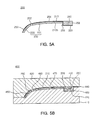
- FIG. 5A is a schematic cross-sectional view taken along line A-A of FIGS. 3 and 4 ;
- FIG. 5B is a schematic cross-sectional view illustrating how a mold for manufacturing an antenna pattern frame is filled with a resin material in order to manufacture an antenna pattern frame depicted in FIG. 5A ;
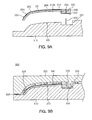
- FIG. 6A is a schematic cross-sectional view illustrating an antenna pattern frame according to another exemplary embodiment of the present invention.
- FIG. 6B is a schematic cross-sectional view illustrating how a mold for manufacturing an antenna pattern frame is filled with a resin material in order to manufacture the antenna pattern frame depicted in FIG. 6A ;
- FIG. 7 is an exploded perspective view illustrating a case of a mobile communications terminal, an electronic device in which the antenna pattern radiator according to an exemplary embodiment of the present invention is embedded;
- FIG. 8 is a schematic view illustrating a method of manufacturing the case of an electronic device in which the antenna pattern radiator according to an exemplary embodiment of the present invention is embedded;
- FIG. 9A is a schematic cross-sectional view illustrating how an antenna pattern radiator is inserted into a mold for manufacturing an electronic device according to an exemplary embodiment of the present invention.
- FIG. 9B is a schematic cross-sectional view illustrating how a resin material is provided to the mold depicted in FIG. 9A ;
- FIG. 10A is a schematic cross-sectional view illustrating how an antenna pattern radiator is inserted into a mold for manufacturing an electronic device according to another exemplary embodiment of the present invention.
- FIG. 10B is a schematic cross-sectional view illustrating how a resin material is provided to the mold depicted in FIG. 10A .
- FIG. 1 is a schematic perspective view, with a cut-away portion, of a case of a mobile communications terminal, which is an electronic device, according to an exemplary embodiment.
- FIG. 2 is a schematic perspective view illustrating a radiator used in manufacturing an antenna pattern frame according to an exemplary embodiment.
- FIG. 3 is a schematic perspective view illustrating an antenna pattern frame according to an exemplary embodiment.
- FIG. 4 is a rear perspective view illustrating the antenna pattern frame depicted in FIG. 3 .
- a radiator 250 provided with an antenna pattern according to an exemplary embodiment of the present invention, is embedded in the case 110 of a mobile communications terminal 100.
- an antenna pattern frame 200 needs to be provided such that the radiator 220 having the antenna pattern is formed on a radiator frame 210.
- the antenna pattern frame 200 may include the radiator 250 having an antenna pattern portion 210, a connection terminal portion 220, and the radiator frame 230.
- the radiator 250 formed of a conductive material such as aluminum or copper, may receive an external signal and send the received external signal to a signal processor of an electronic device such as a mobile communications terminal 100. Further, the radiator 250 may have the antenna pattern portion 210, which is a meander line antenna pattern, in order to receive external signals with various bands.
- the antenna pattern portion 210 receiving external signals, and the connection terminal portion 220 contacting a circuit board of an electronic device to transmit the external signal to the electronic device may be disposed in different planes.
- the radiator 250 may have a three-dimensional structure by being bent such that the antenna pattern portion 210 and the connection terminal portion 220 are disposed in different planes.
- the antenna pattern portion 210 and the connection terminal portion 220 may be connected by a connection portion 256.
- connection portion 256 may allow the antenna pattern portion 210 and the connection terminal portion 220 to be placed in different planes, that is, on one side 210a of the radiator frame 230 and on the other side 210b thereof, respectively.
- the connection terminal portion 220 which is not embedded in the case 110 of an electronic device, may be exposed to the other side 210b of the antenna pattern frame 200.
- the radiator 250 may be bent to provide the antenna pattern portion 210, the connection terminal portion 220, and the connection portion 256 connected therebetween.
- the radiator 250 has a three-dimensional curved shape.
- a radiator support portion 258 may protrude from the other side 210b of the radiator frame 230.
- the radiator support portion 258 may firmly support the connection portion 256 and the connection terminal portion 220 exposed to the other side 210b.
- the radiator support portion 258 may be formed by providing a resin material to the connection portion 256 and one side of the connection terminal portion 220 in a molding process using a mold 400 (See FIG. 6 ) to be described later.
- the radiator support portion 258 has a support hole 260 formed therein.
- a support boss 550 formed in a mold 500 (see FIG. 9B ) is inserted into this support hole 260 at the time of injection molding for forming an electronic device case 110, in which the radiator frame 230 is embedded, within the internal space 540 of the mold 500. In such a manner, the radiator frame 230 is fixed and supported in the internal space of the mold 500.
- the antenna pattern frame 200 may be fitted into the internal space 540 by the use of the support boss 550 formed in the mold 500, so that the degradation of transmission or reception at the connection terminal portion 220 is prevented.
- the radiator support portion 258 may include a hydraulic recess 270 having the same function as the support hole 260.
- a resin material flows into the hydraulic recess 270 at the time of injection molding for forming an electronic device case 110, in which the radiator frame 230 is embedded, within the internal space 540 of a mold 500 (see FIG. 10B ) .
- the radiator frame 230 is fixed and supported in the internal space of the mold 500.
- the antenna pattern frame 200 may be fitted into the internal space 540 by the resin material filling the hydraulic recess 270, so that the degradation of transmission or reception at the connection terminal portion 220 is prevented.
- Both a guide pin hole 252 and contact pin holes 254 may be formed in the radiator 250, and these holes will be described later.
- connection terminal portion 220 transmits a received external signal to an electronic device, and may be formed by bending, forming or drawing a part of the radiator 250.
- connection terminal portion 220 may be manufactured separately from the radiator 250, and then connected to the radiator 250.
- the connection terminal portion 220 may be connected to a terminal 310 of a circuit board 300.
- the radiator frame 230 may have a three-dimensional structure consisting of a straight portion 231 having a flat profile and a curved portion 233 with a curvature.
- the radiator 250 may have flexibility such that the radiator 250 can be disposed along the curved portion 233 of the radiator frame 230.
- the radiator frame 230 is produced by injection-molding. While the antenna pattern portion 210 may be formed on one side 210a of the radiator frame 230, the connection terminal portion 220 may be formed on the other side 210b opposite to the one side 210a.
- the one side 210a of the radiator frame 230, on which the antenna pattern portion 210 is formed, is bonded to the inside of the electronic device case 120, so that the antenna pattern can be embedded in the electronic device case 110.
- the antenna pattern portion 210 receiving external signals and the connection terminal portion 220 transmitting the received external signals to the electronic device may be arranged in different planes.
- FIG. 5A is a schematic cross-sectional view taken along line A-A in FIGS. 3 and 4 .
- FIG. 5B is a schematic cross-sectional view illustrating how a mold for manufacturing an antenna pattern frame is filled with a resin material in order to manufacture the antenna pattern frame depicted in FIG. 5A .
- a guide pin hole 252 or contact pin holes 254 may be formed in the radiator 250 of the antenna pattern frame 200 according to an exemplary embodiment.
- the radiator 250 may have the guide pin hole 252 in which the guide pin 480 of a mold 400 is placed so as to prevent the radiator 250 from moving on the radiator frame 230.
- the radiator 250 may also have the contact pin hole 254 in which a contact pin 470 of the mold 400 is placed so as to prevent the radiator 250 from moving on the radiator frame 230.
- the contact pin 470 and the guide pin 480 may be formed on the radiator 250. After molding, the radiator frame 230 under the contact pin 470 is full, while there is a hole in the radiator frame 230 under the guide pin 480.
- the contact pin 470 inserted into the contact pin hole 254 formed in the radiator 250, serves to prevent the radiator 250 from moving horizontally within the mold 400 for manufacturing the antenna pattern frame 200.
- the guide pin 480 inserted into the guide pin hole 252 formed in the radiator 250, serves to prevent the radiator 250 from moving vertically within the mold 400 for manufacturing the antenna pattern frame 200.
- the radiator 250 after provided, is disposed in the internal space 450 of the mold 400.
- the internal space 450 is created when an upper mold 420 and a lower mold 410 are joined. Recesses formed in the upper mold 420 or the lower mold 410 become the internal space 450 as the upper and lower molds 420 and 410 are joined.
- the guide pin 480, the contact pin 470, or the guide pin 480 and the contact pin 470 formed on the upper or lower mold 410 and 420 are placed in or contact the guide pin hole 252, the contact pin hole 254 or the guide pin hole 252 and the contact pin hole 254 formed in the antenna pattern portion 210, so that the radiator 250 can be fitted into the internal space 450.
- the internal space 450 is filled with a resin material so as to form the radiator frame 230 allowing the antenna pattern portion 210 to be embedded in the electronic device case 110.
- a resin material injection portion 440 may be formed in the upper mold 410, the lower mold 420 or the upper and lower molds 410 and 420.
- the resin material injection portion 440 allows a resin material to be introduced into the internal space 450 created when the upper and lower molds 410 and 420 are joined. In such a way, the radiator frame 230, allowing the antenna pattern portion 210 to be embedded in the electronic device case 110, is formed in the internal space 450.
- the resin material is provided such that the radiator 250 is on the same level as the radiator frame 230. This improves the flow of a resin material when injection molding for manufacturing the electronic device case 110 is performed after placing the radiator frame 230 into a mold for manufacturing the electronic device case 110 in which an antenna pattern is embedded.
- the internal space 450 of the upper or lower mold 410 or 420 may have a curved portion, so that the radiator frame 230 has a curved portion.
- the internal space 450 of the upper and lower molds 410 and 420 receives the connection terminal portion 220, and may have a radiator support portion forming recess 460 allowing for the formation of the radiator support portion 258 supporting the connection terminal portion 220.
- the radiator support portion forming recess 460 is filled with the resin material introduced through the resin material injection hole 440, thereby forming the radiator support portion 258 in the antenna pattern frame 220.
- the upper mold 410, the lower mold 420 or the upper and lower molds 410 and 420 may include a compression pin 430 on the upper mold 410, the lower mold 420 or the upper and lower molds 410 and 420.
- the compression pin 430 compresses the connection terminal portion 220 so that the connection terminal portion 220 contacts the support portion forming recess 460.
- the compression pin 430 may prevent the resin material from flowing under the connection terminal portion 220. If a part of the connection terminal portion 220 is covered with an injection-molded object, an electrical connection may become unstable. The compression pin 430 may serve to prevent this unstable electrical connection.
- the compression pin 430 allows for the formation of the support hole 260 in the antenna pattern frame 200 since the resin material is blocked in the portion where the compression pin 430 is formed.
- a support boss 550 (see FIGS. 9A and 9B ), formed in the mold 500 (see FIG. 9B ), is inserted into the support hole 260, formed by the compression pin 430.
- the support hole 260 formed by the compression pin 430, serves to fix and support the radiator frame 230 in the inner space of the mold 500 (see FIG. 9B ) .
- FIG. 6A is a schematic cross-sectional view illustrating an antenna pattern frame according to another exemplary embodiment.
- FIG. 6B is a schematic cross-sectional view illustrating how a resin material flows into a mold for manufacturing an antenna pattern frame.
- the antenna pattern frame 200 may include a hydraulic recess 270.
- the hydraulic recess 270 may be formed by a hydraulic recess forming pin 490 formed on the upper mold 410, the lower mold 420 or the upper and lower molds 410 and 420.
- the length of the hydraulic recess forming pin 490 does not need to be fixed, and may be set to be long enough to fix and support the radiator frame 230 within the internal space of a mold for injection molding the electronic device case 110 in which the radiator frame 230 is embedded.
- FIG. 7 is an exploded perspective view illustrating a case of a mobile communications terminal, which is an electronic device in which an antenna pattern radiator according to an exemplary embodiment is embedded.
- a case 110 of an electronic device (hereinafter also “electronic device case"), in which the antenna pattern radiator 200 according to an exemplary embodiment is embedded, may include the radiator 250, the radiator frame 230, and the case frame 120.
- radiator 250 and the radiator frame 230 A description of the radiator 250 and the radiator frame 230, described in the above embodiment, will be omitted.
- the case frame 120 covers one side of the radiator frame 230 on which the antenna pattern portion 210 is disposed, thereby embedding the antenna pattern potion 210 between the case frame 120 and the radiator frame 230.
- radiator frame 230 and the case frame 120 may be integrated without having boundaries therebetween.
- the electronic device case 110 is viewed from the rear side, only the connection terminal portion 220 is exposed, while the antenna pattern portion 210 is unseen.
- the radiator frame 230, the case frame 120, or the radiator frame 230 and the case frame 120 may be formed by injection molding.
- the radiator frame 230 and the case frame 120 are provided as separate injection-molded units, the radiator frame 230 including the radiator 250 is bonded to the case frame 120.
- the case frame 120 is injection-molded so as to be integrated with the radiator frame 230. That is, double injection molding may be performed.
- the radiator frame is put into the mold 500 and insert-injection is performed, such that the radiator frame 230 and the case frame 120 are integrated.
- the guide pin hole 252 or the contact pin hole 254 formed in the radiator frame 230 may be coupled with a guide pin or a contact pin formed in the mold 500, thereby preventing the antenna pattern frame 200 from moving within the mold 500.
- FIG. 8 is a schematic view illustrating a method of manufacturing an electronic device case in which an antenna pattern radiator is embedded.
- the case frame 120 is a separate injection-molded part having a radiator receiving space 115 corresponding to the radiator frame 230.
- An electronic device case 110 in which an antenna pattern radiator is embedded may be manufactured by bonding the radiator frame 230 to the radiator receiving space 115.
- An adhesive layer 495 may be formed on the surface of the radiator 250 of the antenna pattern frame 200.
- case frame 120 may have a projection 430, formed by a resin material introduced when the radiator frame 230 is embedded in the electronic device case 110 being injection-molded.
- FIGS. 9A and 9B and FIGS. 10A and 10B are schematic cross-sectional views illustrating how an antenna pattern radiator is inserted into a mold for manufacturing an electronic device and how a resin material is provided in order to manufacture an electronic device case according to exemplary embodiments.
- the antenna pattern frame 200 may be supported and fixed, by its support hole 260, in the internal space 540 of the mold 500 for manufacturing an electronic device case according to an exemplary embodiment.
- the support boss 260 of the lower mold 510 inserted into the support hole 250, supports and fixes the antenna pattern frame 200, thereby preventing defects caused by the protrusion of the exterior, standing against injection pressure during the injection molding, and preventing the degradation in transmission and reception at the antenna pattern portion.
- the support boss 260 may extend to the same length as the thickness of the electronic device case 110 formed by the introduction of a resin material.
- the support boss 260 inserted into the support hole 260 may help to achieve desirable flow effects.
- the support boss 260 is illustrated in FIG. 9 as being formed on the lower mold 510. However, the invention is not limited to this illustration, and the support boss 260 may be formed on the upper mold 520.
- the radiator frame 230 is placed in the mold 500 for manufacturing an electronic device case, which has the internal space therein, and a resin material is introduced thereinto, thereby integrating the radiator frame 230 with the electronic device case 110.
- the radiator frame 230 and the case frame 120 may be formed without having a boundary therebetween.
- the internal space 540 of the mold 500 may include a curve forming portion 525 shaping the electronic device case 110 to have a curved portion.
- the lower mold 510 may have an insertion recess 505 in which the radiator support portion 258 of the antenna pattern frame 200 is inserted.
- the protruding radiator support portion 258 is received in the insertion recess 505.
- the insertion recess 505 may be greater than the radiator support portion 258 in order to fix the antenna pattern frame 200.
- the radiator support portion 258 is inserted into the insertion recess 505, and a resin material is inserted into the remaining space therein. In such a manner, the antenna pattern frame 200 is integrated with the electronic device case.
- a resin material injection portion 530 may be formed in the upper mold 510, the lower mold 520 or the upper and lower molds 510 and 520.
- the resin material injection portion 530 allows a resin material to be introduced into the internal space 540 created when the upper and lower molds 510 and 520 are joined. In such a way, the electronic device case 120 is formed in the internal space 540.
- the radiator frame 230 also includes a guide pin hole or a contact pin hole.
- the guide pin hole or the contact pin hole may be fixed to the guide pin or the contact pin formed in the mold 500, so that the radiator frame 230 is prevented from moving within the mold 500.
- the antenna pattern frame 200 within the mold 500 for manufacturing an electronic device case may be supported and fixed in the internal space 540 by the hydraulic recess 270.
- the resin material introduced into the hydraulic recess 270 supports and fixes the antenna pattern frame 200, thereby preventing defects caused by the protrusion of the exterior, standing against injection pressure during the injection molding and preventing the degradation in transmission and reception at the antenna pattern portion.
- the antenna pattern frame 200 may be supported and fixed in the internal space 540 of the mold 500.
- the antenna pattern frame 200 within the mold 500 for manufacturing the electronic device case may be supported and fixed in the internal space 540 of the mold 500 by the support hole 260 or the hydraulic recess 270, thereby preventing defects caused by the protrusion of the exterior, standing against injection pressure during the injection molding and preventing the degradation in transmission and reception at the antenna pattern portion.
- an antenna pattern frame and a mold for manufacturing an electronic device case including the same can prevent defects caused by the protrusion of the exterior, stand against injection pressure during the injection molding and prevent the degradation in transmission and reception at the antenna pattern portion, when an electronic device case in which an antenna radiator is embedded is injection-molded.
Landscapes
- Engineering & Computer Science (AREA)
- Manufacturing & Machinery (AREA)
- Mechanical Engineering (AREA)
- Computer Networks & Wireless Communication (AREA)
- Details Of Aerials (AREA)
- Support Of Aerials (AREA)
- Telephone Set Structure (AREA)
- Moulds For Moulding Plastics Or The Like (AREA)
- Injection Moulding Of Plastics Or The Like (AREA)
Abstract
In a further embodiment, the radiator frame comprises a support hole in which a support boss is inserted so that the radiator frame contacts the mold.
Description
- This application claims the priority of Korean Patent Application No.
10-2010-0017247 filed on February 25, 2010 - The present invention relates to an antenna pattern frame and a mold for manufacturing an electronic device case including the same, and more particularly, to an antenna pattern frame having a radiator on a surface thereof such that an antenna radiator is embedded in an electronic device case, and a mold for manufacturing an electronic device case including the same.
- Mobile communications terminals such as cellular phones, personal digital assistants (PDAs) and laptop computers, which support wireless communications, are indispensable devices in modern society. Functions including CDMA, wireless LANs, GSM and DMB have been added to these mobile communications terminals. One of the most important components that enable these functions is associated with antennas.
- Antennas being used in these mobile communications terminals have advanced from external antennas, such as rod antennas or helical antennas, to internal antennas that are disposed inside terminals.
- External antennas are susceptible to damage by external shock, while internal antennas increase the volume of terminals.
- In order to solve these problems, research has been undertaken to manufacture antennas that are formed integrally with mobile communications terminals.
- An aspect of the present invention provides an antenna pattern frame and a mold for manufacturing an electronic device case including the same, capable of stably fixing an antenna pattern frame to the mold for manufacturing an electronic device case so as to prevent the protrusion thereof to the exterior, and protecting an antenna connection terminal from injection liquid.
- According to an aspect of the present invention, there is provided an antenna pattern frame including: a radiator including an antenna pattern portion transmitting and receiving a signal and a connection terminal portion allowing the signal to be transmitted to and received from a circuit board of an electronic device; and a radiator frame manufactured by injection molding on the radiator, allowing the antenna pattern portion to be embedded in a case of the electronic device, and supporting the radiator. The radiator frame includes a hydraulic recess introducing a resin material to a mold for manufacturing a case of the electronic device in which the radiator is embedded through injection molding, so that the radiator frame contacts the mold by injection pressure.
- The radiator may include a connection portion forming a part of the radiator and connecting the connection terminal portion with the antenna pattern portion so that the antenna pattern portion is disposed on one side of the radiator frame and the connection terminal portion is disposed on the other side thereof, which is opposite to the one side.
- The connection terminal portion may be supported by a radiator support portion protruding from the other side of the radiator frame, which is opposite to the one side thereof on which the antenna pattern portion is disposed.
- The hydraulic recess may be formed in the radiator support portion.
- According to another aspect of the present invention, there is provided an antenna pattern frame including: a radiator including an antenna pattern portion transmitting and receiving a signal and a connection terminal portion allowing the signal to be transmitted to and received from a circuit board of an electronic device; and a radiator frame manufactured by injection molding on the radiator, allowing the antenna pattern portion to be embedded in a case of the electronic device, and supporting the radiator. The radiator frame includes a support hole in which a support boss, formed in a mold for manufacturing a case of the electronic device in which the radiator is embedded through injection molding, is inserted so that the radiator frame contacts the mold.
- The radiator may include a connection portion forming a part of the radiator and connecting the connection terminal portion with the antenna pattern portion so that the antenna pattern portion is disposed on one side of the radiator frame and the connection terminal portion is disposed on the other side thereof, which is opposite to the one side.
- The connection terminal portion may be supported by a radiator support portion protruding from the other side of the radiator frame, which is opposite to the one side thereof on which the antenna pattern portion is disposed.
- The support hole may be formed in the radiator support portion.
- According to another aspect of the present invention, there is provided a mold for manufacturing an electronic device case, the mold including: upper and lower molds receiving an antenna pattern frame including an antenna pattern portion transmitting and receiving a signal, a connection terminal portion allowing the signal to be transmitted to and received from a circuit board of an electronic device, and a radiator frame supporting the radiator; and a resin material injection portion provided through the upper mold, the lower mold, or the upper and lower molds, the resin material injection portion through which a resin material is injected into an internal space, created between the upper and lower molds when the upper and lower molds are joined, so that the antenna pattern portion of the radiator frame is embedded in a case of the electronic device. The radiator frame includes a hydraulic recess introducing a resin material into the internal space for the injection molding of the case of the electronic device, so that the radiator frame contacts the mold by injection pressure, and the electronic device case in which the radiator frame is embedded is injection-molded by the internal space.
- The connection terminal portion may contact a radiator support portion protruding from an opposite side to a side on which the antenna pattern portion of the radiator frame is formed, and the lower mold may include an insertion recess receiving the radiator support portion.
- The insertion recess may be greater than the radiator support portion.
- The lower mold may contact one side of the antenna pattern frame, and the upper mold may create a space with the other side of the antenna pattern frame, so that a resin material is introduced into the space.
- The internal space may be provided with a curve forming portion so that the electronic device case has a curved portion.
- According to another aspect of the present invention, there is provided a mold for manufacturing an electronic device case, the mold including: upper and lower molds receiving an antenna pattern frame including an antenna pattern portion transmitting and receiving a signal, a connection terminal portion allowing the signal to be transmitted to and received from a circuit board of an electronic device, and a radiator frame supporting the radiator; and a resin material injection portion provided through the upper mold, the lower mold, or the upper and lower molds, the resin material injection portion through which a resin material is injected into an internal space, created between the upper and lower molds when the upper and lower molds are joined, so that the antenna pattern portion of the radiator frame is embedded in a case of the electronic device. The upper mold, the lower mold or the upper and lower molds include a support boss fixing and supporting the radiator frame to the internal space; and the radiator frame includes a support hole in which the support boss is inserted so that the radiator frame contacts the mold, and the electronic device case in which the radiator frame is embedded is inj ection-molded by the internal space.
- The connection terminal portion may contact a radiator support portion protruding from an opposite side to a side on which the antenna pattern portion of the radiator frame is formed, and the lower mold may include an insertion recess receiving the radiator support portion.
- The insertion recess may be greater than the radiator support portion.
- The support boss may be formed in the insertion recess.
- The support boss may contact the upper mold.
- The lower mold may contact one side of the antenna pattern frame, and the upper mold may create a space with the other side of the antenna pattern frame so that a resin material is introduced into the space.
- The internal space may have a curve forming portion so that the electronic device case has a curved portion
- The above and other aspects, features and other advantages of the present invention will be more clearly understood from the following detailed description taken in conjunction with the accompanying drawings, in which:
-
FIG. 1 is a schematic perspective view, with a cut-away portion, of a case of a mobile communications terminal, which is an electronic device, according to an exemplary embodiment of the present invention; -
FIG. 2 is a schematic perspective view illustrating a radiator used in manufacturing an antenna pattern frame according to an exemplary embodiment of the present invention; -
FIG. 3 is a schematic perspective view illustrating an antenna pattern frame according to an exemplary embodiment of the present invention; -
FIG. 4 is a rear perspective view illustrating the antenna pattern frame depicted inFIG. 3 ; -
FIG. 5A is a schematic cross-sectional view taken along line A-A ofFIGS. 3 and4 ; -
FIG. 5B is a schematic cross-sectional view illustrating how a mold for manufacturing an antenna pattern frame is filled with a resin material in order to manufacture an antenna pattern frame depicted inFIG. 5A ; -
FIG. 6A is a schematic cross-sectional view illustrating an antenna pattern frame according to another exemplary embodiment of the present invention; -
FIG. 6B is a schematic cross-sectional view illustrating how a mold for manufacturing an antenna pattern frame is filled with a resin material in order to manufacture the antenna pattern frame depicted inFIG. 6A ; -
FIG. 7 is an exploded perspective view illustrating a case of a mobile communications terminal, an electronic device in which the antenna pattern radiator according to an exemplary embodiment of the present invention is embedded; -
FIG. 8 is a schematic view illustrating a method of manufacturing the case of an electronic device in which the antenna pattern radiator according to an exemplary embodiment of the present invention is embedded; -
FIG. 9A is a schematic cross-sectional view illustrating how an antenna pattern radiator is inserted into a mold for manufacturing an electronic device according to an exemplary embodiment of the present invention; -
FIG. 9B is a schematic cross-sectional view illustrating how a resin material is provided to the mold depicted inFIG. 9A ; -
FIG. 10A is a schematic cross-sectional view illustrating how an antenna pattern radiator is inserted into a mold for manufacturing an electronic device according to another exemplary embodiment of the present invention; and -
FIG. 10B is a schematic cross-sectional view illustrating how a resin material is provided to the mold depicted inFIG. 10A . - Exemplary embodiments of the present invention will now be described in detail with reference to the accompanying drawings. The invention may, however, be embodied in many different forms and should not be construed as being limited to the embodiments set forth herein. While those skilled in the art could readily devise many other varied embodiments that incorporate the teachings of the present invention through the addition, modification or deletion of elements, such embodiments may fall within the scope of the present invention.
- The same or equivalent elements are referred to by the same reference numerals throughout the specification.
-
FIG. 1 is a schematic perspective view, with a cut-away portion, of a case of a mobile communications terminal, which is an electronic device, according to an exemplary embodiment.FIG. 2 is a schematic perspective view illustrating a radiator used in manufacturing an antenna pattern frame according to an exemplary embodiment.FIG. 3 is a schematic perspective view illustrating an antenna pattern frame according to an exemplary embodiment.FIG. 4 is a rear perspective view illustrating the antenna pattern frame depicted inFIG. 3 . - Referring to
FIGS. 1 through 4 , aradiator 250, provided with an antenna pattern according to an exemplary embodiment of the present invention, is embedded in thecase 110 of amobile communications terminal 100. In order that theradiator 250 having the antenna pattern be embedded in thecase 110, anantenna pattern frame 200 needs to be provided such that theradiator 220 having the antenna pattern is formed on aradiator frame 210. - The
antenna pattern frame 200, according to an exemplary embodiment, may include theradiator 250 having anantenna pattern portion 210, aconnection terminal portion 220, and theradiator frame 230. - The
radiator 250, formed of a conductive material such as aluminum or copper, may receive an external signal and send the received external signal to a signal processor of an electronic device such as amobile communications terminal 100. Further, theradiator 250 may have theantenna pattern portion 210, which is a meander line antenna pattern, in order to receive external signals with various bands. - As for the
radiator 250, theantenna pattern portion 210 receiving external signals, and theconnection terminal portion 220 contacting a circuit board of an electronic device to transmit the external signal to the electronic device may be disposed in different planes. - Moreover, the
radiator 250 may have a three-dimensional structure by being bent such that theantenna pattern portion 210 and theconnection terminal portion 220 are disposed in different planes. Here, theantenna pattern portion 210 and theconnection terminal portion 220 may be connected by aconnection portion 256. - The
connection portion 256 may allow theantenna pattern portion 210 and theconnection terminal portion 220 to be placed in different planes, that is, on oneside 210a of theradiator frame 230 and on theother side 210b thereof, respectively. Theconnection terminal portion 220, which is not embedded in thecase 110 of an electronic device, may be exposed to theother side 210b of theantenna pattern frame 200. - That is, the
radiator 250 may be bent to provide theantenna pattern portion 210, theconnection terminal portion 220, and theconnection portion 256 connected therebetween. Thus, theradiator 250 has a three-dimensional curved shape. - In order to support the
radiator 250 having a three-dimensional curved shape, aradiator support portion 258 may protrude from theother side 210b of theradiator frame 230. - The
radiator support portion 258 may firmly support theconnection portion 256 and theconnection terminal portion 220 exposed to theother side 210b. - Here, the
radiator support portion 258 may be formed by providing a resin material to theconnection portion 256 and one side of theconnection terminal portion 220 in a molding process using a mold 400 (SeeFIG. 6 ) to be described later. - Here, the
radiator support portion 258 has asupport hole 260 formed therein. Asupport boss 550 formed in a mold 500 (seeFIG. 9B ) is inserted into thissupport hole 260 at the time of injection molding for forming anelectronic device case 110, in which theradiator frame 230 is embedded, within theinternal space 540 of themold 500. In such a manner, theradiator frame 230 is fixed and supported in the internal space of themold 500. - The
antenna pattern frame 200 may be fitted into theinternal space 540 by the use of thesupport boss 550 formed in themold 500, so that the degradation of transmission or reception at theconnection terminal portion 220 is prevented. - Further, the
radiator support portion 258 may include ahydraulic recess 270 having the same function as thesupport hole 260. A resin material flows into thehydraulic recess 270 at the time of injection molding for forming anelectronic device case 110, in which theradiator frame 230 is embedded, within theinternal space 540 of a mold 500 (seeFIG. 10B ) . Thus, theradiator frame 230 is fixed and supported in the internal space of themold 500. - The
antenna pattern frame 200 may be fitted into theinternal space 540 by the resin material filling thehydraulic recess 270, so that the degradation of transmission or reception at theconnection terminal portion 220 is prevented. - Both a
guide pin hole 252 and contact pin holes 254 may be formed in theradiator 250, and these holes will be described later. - The
connection terminal portion 220 transmits a received external signal to an electronic device, and may be formed by bending, forming or drawing a part of theradiator 250. - Moreover, the
connection terminal portion 220 may be manufactured separately from theradiator 250, and then connected to theradiator 250. Theconnection terminal portion 220 may be connected to aterminal 310 of acircuit board 300. - The
radiator frame 230 may have a three-dimensional structure consisting of astraight portion 231 having a flat profile and acurved portion 233 with a curvature. Theradiator 250 may have flexibility such that theradiator 250 can be disposed along thecurved portion 233 of theradiator frame 230. - The
radiator frame 230 is produced by injection-molding. While theantenna pattern portion 210 may be formed on oneside 210a of theradiator frame 230, theconnection terminal portion 220 may be formed on theother side 210b opposite to the oneside 210a. - The one
side 210a of theradiator frame 230, on which theantenna pattern portion 210 is formed, is bonded to the inside of theelectronic device case 120, so that the antenna pattern can be embedded in theelectronic device case 110. - As for the structure of the
radiator 250 embedded in theelectronic device case 110, theantenna pattern portion 210 receiving external signals and theconnection terminal portion 220 transmitting the received external signals to the electronic device may be arranged in different planes. -
FIG. 5A is a schematic cross-sectional view taken along line A-A inFIGS. 3 and4 .FIG. 5B is a schematic cross-sectional view illustrating how a mold for manufacturing an antenna pattern frame is filled with a resin material in order to manufacture the antenna pattern frame depicted inFIG. 5A . - Referring to
FIG. 5A , aguide pin hole 252 or contact pin holes 254 may be formed in theradiator 250 of theantenna pattern frame 200 according to an exemplary embodiment. - The
radiator 250 may have theguide pin hole 252 in which theguide pin 480 of amold 400 is placed so as to prevent theradiator 250 from moving on theradiator frame 230. - The
radiator 250 may also have thecontact pin hole 254 in which acontact pin 470 of themold 400 is placed so as to prevent theradiator 250 from moving on theradiator frame 230. - The
contact pin 470 and theguide pin 480 may be formed on theradiator 250. After molding, theradiator frame 230 under thecontact pin 470 is full, while there is a hole in theradiator frame 230 under theguide pin 480. - The
contact pin 470, inserted into thecontact pin hole 254 formed in theradiator 250, serves to prevent theradiator 250 from moving horizontally within themold 400 for manufacturing theantenna pattern frame 200. - The
guide pin 480, inserted into theguide pin hole 252 formed in theradiator 250, serves to prevent theradiator 250 from moving vertically within themold 400 for manufacturing theantenna pattern frame 200. - Referring to
FIG. 5B , theradiator 250, after provided, is disposed in theinternal space 450 of themold 400. - The
internal space 450 is created when anupper mold 420 and alower mold 410 are joined. Recesses formed in theupper mold 420 or thelower mold 410 become theinternal space 450 as the upper andlower molds - When the
upper mold 420 and thelower mold 410 are joined, theguide pin 480, thecontact pin 470, or theguide pin 480 and thecontact pin 470 formed on the upper orlower mold guide pin hole 252, thecontact pin hole 254 or theguide pin hole 252 and thecontact pin hole 254 formed in theantenna pattern portion 210, so that theradiator 250 can be fitted into theinternal space 450. - The
internal space 450 is filled with a resin material so as to form theradiator frame 230 allowing theantenna pattern portion 210 to be embedded in theelectronic device case 110. - A resin
material injection portion 440 may be formed in theupper mold 410, thelower mold 420 or the upper andlower molds material injection portion 440 allows a resin material to be introduced into theinternal space 450 created when the upper andlower molds radiator frame 230, allowing theantenna pattern portion 210 to be embedded in theelectronic device case 110, is formed in theinternal space 450. - The resin material is provided such that the
radiator 250 is on the same level as theradiator frame 230. This improves the flow of a resin material when injection molding for manufacturing theelectronic device case 110 is performed after placing theradiator frame 230 into a mold for manufacturing theelectronic device case 110 in which an antenna pattern is embedded. - In this case, the
internal space 450 of the upper orlower mold radiator frame 230 has a curved portion. - The
internal space 450 of the upper andlower molds connection terminal portion 220, and may have a radiator supportportion forming recess 460 allowing for the formation of theradiator support portion 258 supporting theconnection terminal portion 220. - The radiator support
portion forming recess 460 is filled with the resin material introduced through the resinmaterial injection hole 440, thereby forming theradiator support portion 258 in theantenna pattern frame 220. - Further, the
upper mold 410, thelower mold 420 or the upper andlower molds compression pin 430 on theupper mold 410, thelower mold 420 or the upper andlower molds compression pin 430 compresses theconnection terminal portion 220 so that theconnection terminal portion 220 contacts the supportportion forming recess 460. - The
compression pin 430 may prevent the resin material from flowing under theconnection terminal portion 220. If a part of theconnection terminal portion 220 is covered with an injection-molded object, an electrical connection may become unstable. Thecompression pin 430 may serve to prevent this unstable electrical connection. - In addition, the
compression pin 430 allows for the formation of thesupport hole 260 in theantenna pattern frame 200 since the resin material is blocked in the portion where thecompression pin 430 is formed. - When injection molding is performed on the
electronic device case 110 in which theradiator frame 230 is embedded, a support boss 550 (seeFIGS. 9A and 9B ), formed in the mold 500 (seeFIG. 9B ), is inserted into thesupport hole 260, formed by thecompression pin 430. Thus, thesupport hole 260, formed by thecompression pin 430, serves to fix and support theradiator frame 230 in the inner space of the mold 500 (seeFIG. 9B ) . -
FIG. 6A is a schematic cross-sectional view illustrating an antenna pattern frame according to another exemplary embodiment.FIG. 6B is a schematic cross-sectional view illustrating how a resin material flows into a mold for manufacturing an antenna pattern frame. - Referring to
FIGS. 6A and 6B , theantenna pattern frame 200 may include ahydraulic recess 270. Thehydraulic recess 270 may be formed by a hydraulic recess forming pin 490 formed on theupper mold 410, thelower mold 420 or the upper andlower molds - The length of the hydraulic recess forming pin 490 does not need to be fixed, and may be set to be long enough to fix and support the
radiator frame 230 within the internal space of a mold for injection molding theelectronic device case 110 in which theradiator frame 230 is embedded. -
FIG. 7 is an exploded perspective view illustrating a case of a mobile communications terminal, which is an electronic device in which an antenna pattern radiator according to an exemplary embodiment is embedded. - Referring to
FIG. 7 , acase 110 of an electronic device (hereinafter also "electronic device case"), in which theantenna pattern radiator 200 according to an exemplary embodiment is embedded, may include theradiator 250, theradiator frame 230, and thecase frame 120. - A description of the
radiator 250 and theradiator frame 230, described in the above embodiment, will be omitted. - The
case frame 120 covers one side of theradiator frame 230 on which theantenna pattern portion 210 is disposed, thereby embedding theantenna pattern potion 210 between thecase frame 120 and theradiator frame 230. - Further, the
radiator frame 230 and thecase frame 120 may be integrated without having boundaries therebetween. When theelectronic device case 110 is viewed from the rear side, only theconnection terminal portion 220 is exposed, while theantenna pattern portion 210 is unseen. - The
radiator frame 230, thecase frame 120, or theradiator frame 230 and thecase frame 120 may be formed by injection molding. In particular, if theradiator frame 230 and thecase frame 120 are provided as separate injection-molded units, theradiator frame 230 including theradiator 250 is bonded to thecase frame 120. - The
case frame 120 is injection-molded so as to be integrated with theradiator frame 230. That is, double injection molding may be performed. In detail, the radiator frame is put into themold 500 and insert-injection is performed, such that theradiator frame 230 and thecase frame 120 are integrated. - When the
radiator frame 230 is put into the mold 500 (seeFIGS. 10A and 10B ) for manufacturing an electronic device case, theguide pin hole 252 or thecontact pin hole 254 formed in theradiator frame 230 may be coupled with a guide pin or a contact pin formed in themold 500, thereby preventing theantenna pattern frame 200 from moving within themold 500. -
FIG. 8 is a schematic view illustrating a method of manufacturing an electronic device case in which an antenna pattern radiator is embedded. - Referring to
FIG. 8 , thecase frame 120 is a separate injection-molded part having aradiator receiving space 115 corresponding to theradiator frame 230. Anelectronic device case 110 in which an antenna pattern radiator is embedded may be manufactured by bonding theradiator frame 230 to theradiator receiving space 115. - An
adhesive layer 495 may be formed on the surface of theradiator 250 of theantenna pattern frame 200. - In addition, the
case frame 120 may have aprojection 430, formed by a resin material introduced when theradiator frame 230 is embedded in theelectronic device case 110 being injection-molded. -
FIGS. 9A and 9B andFIGS. 10A and 10B are schematic cross-sectional views illustrating how an antenna pattern radiator is inserted into a mold for manufacturing an electronic device and how a resin material is provided in order to manufacture an electronic device case according to exemplary embodiments. - Referring to
FIGS. 9A and 9B , theantenna pattern frame 200 may be supported and fixed, by itssupport hole 260, in theinternal space 540 of themold 500 for manufacturing an electronic device case according to an exemplary embodiment. - The
support boss 260 of thelower mold 510, inserted into thesupport hole 250, supports and fixes theantenna pattern frame 200, thereby preventing defects caused by the protrusion of the exterior, standing against injection pressure during the injection molding, and preventing the degradation in transmission and reception at the antenna pattern portion. - The
support boss 260 may extend to the same length as the thickness of theelectronic device case 110 formed by the introduction of a resin material. Thesupport boss 260 inserted into thesupport hole 260 may help to achieve desirable flow effects. - The
support boss 260 is illustrated inFIG. 9 as being formed on thelower mold 510. However, the invention is not limited to this illustration, and thesupport boss 260 may be formed on theupper mold 520. - The
radiator frame 230 is placed in themold 500 for manufacturing an electronic device case, which has the internal space therein, and a resin material is introduced thereinto, thereby integrating theradiator frame 230 with theelectronic device case 110. - The
radiator frame 230 and thecase frame 120 may be formed without having a boundary therebetween. - The
internal space 540 of themold 500 may include acurve forming portion 525 shaping theelectronic device case 110 to have a curved portion. - Here, the
lower mold 510 may have aninsertion recess 505 in which theradiator support portion 258 of theantenna pattern frame 200 is inserted. - The protruding
radiator support portion 258 is received in theinsertion recess 505. Theinsertion recess 505 may be greater than theradiator support portion 258 in order to fix theantenna pattern frame 200. - The
radiator support portion 258 is inserted into theinsertion recess 505, and a resin material is inserted into the remaining space therein. In such a manner, theantenna pattern frame 200 is integrated with the electronic device case. - A resin
material injection portion 530 may be formed in theupper mold 510, thelower mold 520 or the upper andlower molds material injection portion 530 allows a resin material to be introduced into theinternal space 540 created when the upper andlower molds electronic device case 120 is formed in theinternal space 540. - Like the
radiator 250, theradiator frame 230 also includes a guide pin hole or a contact pin hole. The guide pin hole or the contact pin hole may be fixed to the guide pin or the contact pin formed in themold 500, so that theradiator frame 230 is prevented from moving within themold 500. - Referring to
FIGS. 10A and 10B , theantenna pattern frame 200 within themold 500 for manufacturing an electronic device case, according to another exemplary embodiment, may be supported and fixed in theinternal space 540 by thehydraulic recess 270. - The resin material introduced into the
hydraulic recess 270 supports and fixes theantenna pattern frame 200, thereby preventing defects caused by the protrusion of the exterior, standing against injection pressure during the injection molding and preventing the degradation in transmission and reception at the antenna pattern portion. - As the resin material flows into the
hydraulic recess 270, theantenna pattern frame 200 may be supported and fixed in theinternal space 540 of themold 500. - As described in the above exemplary embodiments, the
antenna pattern frame 200 within themold 500 for manufacturing the electronic device case may be supported and fixed in theinternal space 540 of themold 500 by thesupport hole 260 or thehydraulic recess 270, thereby preventing defects caused by the protrusion of the exterior, standing against injection pressure during the injection molding and preventing the degradation in transmission and reception at the antenna pattern portion. - As set forth above, according to exemplary embodiments of the invention, an antenna pattern frame and a mold for manufacturing an electronic device case including the same can prevent defects caused by the protrusion of the exterior, stand against injection pressure during the injection molding and prevent the degradation in transmission and reception at the antenna pattern portion, when an electronic device case in which an antenna radiator is embedded is injection-molded.
- While the present invention has been shown and described in connection with the exemplary embodiments, it will be apparent to those skilled in the art that modifications and variations can be made without departing from the spirit and scope of the invention as defined by the appended claims.
Claims (20)
- An antenna pattern frame comprising:a radiator comprising an antenna pattern portion transmitting and receiving a signal and a connection terminal portion allowing the signal to be transmitted to and received from a circuit board of an electronic device; anda radiator frame manufactured by injecting-molding on the radiator, allowing the antenna pattern portion to be embedded in a case of the electronic device, and supporting the radiator,wherein the radiator frame comprises a hydraulic recess introducing a resin material into a mold for manufacturing a case of the electronic device in which the radiator is embedded through injection molding, so that the radiator frame contacts the mold by injection pressure.
- The antenna pattern frame of claim 1, wherein the radiator comprises a connection portion forming a part of the radiator and connecting the connection terminal portion with the antenna pattern portion so that the antenna pattern portion is disposed on one side of the radiator frame and the connection terminal portion is disposed on the other side thereof, which is opposite to the one side.
- The antenna pattern frame of claim 2, wherein the connection terminal portion is supported by a radiator support portion protruding from the other side of the radiator frame, which is opposite to the one side thereof on which the antenna pattern portion is disposed.
- The antenna pattern frame of claim 3, wherein the hydraulic recess is formed in the radiator support portion.
- An antenna pattern frame comprising:a radiator comprising an antenna pattern portion transmitting and receiving a signal and a connection terminal portion allowing the signal to be transmitted to and received from a circuit board of an electronic device; anda radiator frame manufactured by injection molding on the radiator, allowing the antenna pattern portion to be embedded in a case of the electronic device, and supporting the radiator,wherein the radiator frame comprises a support hole in which a support boss, formed in a mold for manufacturing a case of the electronic device in which the radiator is embedded through injection molding, is inserted so that the radiator frame contacts the mold.
- The antenna pattern frame of claim 5, wherein the radiator comprises a connection portion forming a part of the radiator, and connecting the connection terminal portion with the antenna pattern portion so that the antenna pattern portion is disposed on one side of the radiator frame and the connection terminal portion is disposed on the other side thereof, which is opposite to the one side.
- The antenna pattern frame of claim 6, wherein the connection terminal portion is supported by a radiator support portion protruding from the other side of the radiator frame, which is opposite to the one side thereof on which the antenna pattern portion is disposed.
- The antenna pattern frame of claim 7, wherein the support hole is formed in the radiator support portion.
- A mold for manufacturing an electronic device case, the mold comprising:upper and lower molds receiving an antenna pattern frame comprising an antenna pattern portion transmitting and receiving a signal, a connection terminal portion allowing the signal to be transmitted to and received from a circuit board of an electronic device, and a radiator frame supporting the radiator; anda resin material injection portion provided through the upper mold, the lower mold, or the upper and lower molds, the resin material injection portion through which a resin material is injected into an internal space, created between the upper and lower molds when the upper and lower molds are joined, so that the antenna pattern portion of the radiator frame is embedded in a case of the electronic device,wherein the radiator frame comprises a hydraulic recess introducing a resin material into the internal space for the injection molding of the case of the electronic device, so that the radiator frame contacts the mold by injection pressure, and the electronic device case in which the radiator frame is embedded is injection-molded by the internal space.
- The mold of claim 9, wherein the connection terminal portion contacts a radiator support portion protruding from an opposite side to a side on which the antenna pattern portion of the radiator frame is formed, and
the lower mold includes an insertion recess receiving the radiator support portion. - The mold of claim 10, wherein the insertion recess is greater than the radiator support portion.
- The mold of claim 9, wherein the lower mold contacts one side of the antenna pattern frame, and the upper mold creates a space with the other side of the antenna pattern frame, so that a resin material is introduced into the space.
- The mold of claim 9, wherein the internal space is provided with a curve forming portion so that the electronic device case has a curved portion.
- A mold for manufacturing an electronic device case, the mold comprising:upper and lower molds receiving an antenna pattern frame comprising an antenna pattern portion transmitting and receiving a signal, a connection terminal portion allowing the signal to be transmitted to and received from a circuit board of an electronic device, and a radiator frame supporting the radiator; anda resin material injection portion provided through the upper mold, the lower mold, or the upper and lower molds, the resin material injection portion through which a resin material is injected into an internal space, created between the upper and lower molds when the upper and lower molds are joined, so that the antenna pattern portion of the radiator frame is embedded in a case of the electronic devicewherein the upper mold, the lower mold or the upper and lower molds include a support boss fixing and supporting the radiator frame to the internal space; andthe radiator frame includes a support hole in which the support boss is inserted so that the radiator frame contacts the mold, and the electronic device case in which the radiator frame is embedded is injection-molded by the internal space.
- The mold of claim 14, wherein the connection terminal portion contacts a radiator support portion protruding from an opposite side to a side on which the antenna pattern portion of the radiator frame is formed, and
the lower mold includes an insertion recess receiving the radiator support portion. - The mold of claim 15, wherein the insertion recess is greater than the radiator support portion.
- The mold of claim 15, wherein the support boss is formed in the insertion recess.
- The mold of claim 17, wherein the support boss contacts the upper mold.
- The mold of claim 14, wherein the lower mold contacts one side of the antenna pattern frame, and the upper mold creates a space with the other side of the antenna pattern frame so that a resin material is introduced into the space.
- The mold of claim 14, wherein the internal space has a curve forming portion so that the electronic device case has a curved portion.
Applications Claiming Priority (1)
| Application Number | Priority Date | Filing Date | Title |
|---|---|---|---|
| KR20100017247A KR101101622B1 (en) | 2010-02-25 | 2010-02-25 | Antenna pattern frame and electronic device case manufacturing mold including the same |
Publications (1)
| Publication Number | Publication Date |
|---|---|
| EP2361744A1 true EP2361744A1 (en) | 2011-08-31 |
Family
ID=44123423
Family Applications (1)
| Application Number | Title | Priority Date | Filing Date |
|---|---|---|---|
| EP11250206A Withdrawn EP2361744A1 (en) | 2010-02-25 | 2011-02-23 | Antenna pattern frame and mold for manufacturing electronic device case including the same |
Country Status (5)
| Country | Link |
|---|---|
| US (1) | US9035847B2 (en) |
| EP (1) | EP2361744A1 (en) |
| JP (2) | JP5266600B2 (en) |
| KR (1) | KR101101622B1 (en) |
| CN (1) | CN102170040B (en) |
Cited By (1)
| Publication number | Priority date | Publication date | Assignee | Title |
|---|---|---|---|---|
| US11201119B2 (en) | 2018-06-06 | 2021-12-14 | At&S Austria Technologie & Systemtechnik Aktiengesellschaft | RF functionality and electromagnetic radiation shielding in a component carrier |
Families Citing this family (26)
| Publication number | Priority date | Publication date | Assignee | Title |
|---|---|---|---|---|
| EP2446865A1 (en) | 2010-10-28 | 2012-05-02 | Louise Mohn | Thermostimulation apparatus |
| CN102723574A (en) * | 2011-03-31 | 2012-10-10 | 深圳富泰宏精密工业有限公司 | Housing assembly with built-in antenna and electronic device applying same |
| CN102780079A (en) * | 2011-05-09 | 2012-11-14 | 深圳富泰宏精密工业有限公司 | Antenna assembly and manufacture method thereof |
| KR101333093B1 (en) * | 2011-11-17 | 2013-11-26 | 주식회사 우전앤한단 | Case for mobile device having integrally forming antenna and manufacturing method thereof |
| DE102011088259A1 (en) * | 2011-12-12 | 2013-06-13 | Robert Bosch Gmbh | Bar antenna for remote control device for motor car, has metal strip that is formed as transmitter and/or receiver, and is soldered as surface-mounted component to circuit board |
| KR101258445B1 (en) | 2012-01-31 | 2013-04-26 | 주식회사 모비텍 | Internal antenna apparatus and method thereof |
| GB2500633A (en) * | 2012-03-27 | 2013-10-02 | Louise Mohn | Moulding method |
| CN103358459B (en) * | 2012-03-31 | 2015-07-22 | 比亚迪股份有限公司 | Positioning structure of tone cavity sealing bracket and die for manufacturing tone cavity sealing bracket |
| KR101931636B1 (en) | 2012-05-16 | 2018-12-21 | 엘지이노텍 주식회사 | Antenna of telecommunication terminal and manufacturing method thereof |
| KR101353946B1 (en) | 2012-11-22 | 2014-01-22 | 주식회사 에이티앤씨 | A antenna module manufacturing method for a mobile phone |
| KR101397824B1 (en) | 2012-12-14 | 2014-05-20 | 삼성전기주식회사 | Radiator frame having antenna pattern embeded therein, electronic device including thereof, and mould for manufacturing thereof |
| KR101397747B1 (en) | 2012-12-14 | 2014-05-20 | 삼성전기주식회사 | Antenna pattern frame having antenna pattern embeded, electronic device including thereof, method and mould for manufacturing thereof |
| JP6092674B2 (en) * | 2013-03-22 | 2017-03-08 | シャープ株式会社 | Structure, wireless communication device, and method of manufacturing structure |
| KR101405881B1 (en) * | 2013-09-12 | 2014-06-19 | 주식회사 우전앤한단 | Case for mobile device having integrally forming antenna |
| FR3013904B1 (en) * | 2013-11-28 | 2015-12-04 | Commissariat Energie Atomique | ELECTRONIC APPARATUS WITH RADIO ANTENNA FOLDED IN A CASE |
| KR101547131B1 (en) * | 2014-03-20 | 2015-08-25 | 스카이크로스 인코포레이티드 | Antenna with radiator fixed by fusion, and manufacturing method thereof |
| KR20160092875A (en) * | 2015-01-28 | 2016-08-05 | 삼성전기주식회사 | Radiator frame having antenna pattern embeded therein and electronic device including thereof |
| KR20160107480A (en) | 2015-03-04 | 2016-09-19 | 삼성전기주식회사 | Radiator frame, electronic device including thereof, and mould for manufacturing thereof |
| JP2017147537A (en) * | 2016-02-16 | 2017-08-24 | レノボ・シンガポール・プライベート・リミテッド | Electronic equipment and housing for electronic equipment |
| JP6820078B2 (en) * | 2016-10-04 | 2021-01-27 | 富士通コネクテッドテクノロジーズ株式会社 | Housing with built-in antenna and wireless communication device |
| KR101876813B1 (en) * | 2017-12-08 | 2018-07-10 | 주식회사 이엠따블유 | Antenna module and method of manufacturing the same |
| US11139588B2 (en) | 2018-04-11 | 2021-10-05 | Apple Inc. | Electronic device antenna arrays mounted against a dielectric layer |
| CN108493608B (en) * | 2018-05-17 | 2024-03-29 | 深圳市优必选科技有限公司 | Antenna assembly and robot |
| CN109159374A (en) * | 2018-08-31 | 2019-01-08 | 西安易朴通讯技术有限公司 | A kind of mold and two shot process |
| CN110640970B (en) * | 2019-08-26 | 2022-07-15 | 广东长盈精密技术有限公司 | Method for processing functional hole of electronic product shell and insert adopted by same |
| CN110943282B (en) * | 2019-12-12 | 2021-07-02 | 惠州Tcl移动通信有限公司 | Mobile terminal |
Citations (10)
| Publication number | Priority date | Publication date | Assignee | Title |
|---|---|---|---|---|
| US4427615A (en) * | 1980-12-09 | 1984-01-24 | Brdr. Eskesen Aktieselskab | Method of making injection moulded plastic objects with imbedded decorative and/or descriptive prints |
| EP0500219A1 (en) * | 1991-02-18 | 1992-08-26 | Sumitomo Wiring Systems, Ltd. | A method for producing a metal elements-resin insert; a connector block for injectors, and a method for producing the connector block |
| JP2003260724A (en) * | 2002-03-08 | 2003-09-16 | Nissan Motor Co Ltd | Injection molding die and injection molding method |
| US20080138554A1 (en) * | 2006-12-08 | 2008-06-12 | Tokai Rubber Industries, Ltd. | Weld Joint for Fuel Tank |
| KR100932079B1 (en) * | 2009-03-31 | 2009-12-15 | 마상영 | Insert antenna module for portable terminal and manufacturing method thereof |
| US20100271265A1 (en) * | 2009-04-23 | 2010-10-28 | Samsung Electro-Mechanics Co., Ltd. | Antenna pattern frame and method and mold for manufacturing the same |
| US20100271272A1 (en) * | 2009-04-23 | 2010-10-28 | Samsung Electro-Mechanics Co., Ltd. | Antenna pattern frame, method and mold for manufacturing the same, and electronic device |
| US20100271270A1 (en) * | 2009-04-23 | 2010-10-28 | Samsung Electro-Mechanics Co., Ltd. | Electronic device case, method and mold for manufacturing the same, and mobile communications terminal |
| EP2284947A1 (en) * | 2009-08-10 | 2011-02-16 | Samsung Electro-Mechanics Co., Ltd | Antenna pattern frame, method and mold for manufacturing the same, electronic device case having antenna pattern frame embedded therein, and method for manufacturing the same |
| EP2302733A2 (en) * | 2009-09-22 | 2011-03-30 | Samsung Electro-Mechanics Co., Ltd. | Antenna pattern frame, method and mold for manufacturing the same, method for manufacturing an electronic device case, and electronic device |
Family Cites Families (23)
| Publication number | Priority date | Publication date | Assignee | Title |
|---|---|---|---|---|
| JP3502926B2 (en) * | 1993-09-30 | 2004-03-02 | 松下電器産業株式会社 | Antenna unit |
| JP3355756B2 (en) * | 1994-02-09 | 2002-12-09 | 東海化成工業株式会社 | Core injection molding method |
| JP3111824B2 (en) * | 1994-08-31 | 2000-11-27 | 三菱電機株式会社 | Plate antenna for mobile phone and method of manufacturing the same |
| JPH09102709A (en) * | 1995-10-04 | 1997-04-15 | Pioneer Electron Corp | Forming method for microstrip antenna |
| JPH10247817A (en) * | 1997-03-05 | 1998-09-14 | Otsuka Chem Co Ltd | Dielectric resin antenna and manufacture therefor |
| JP2965036B1 (en) * | 1998-09-07 | 1999-10-18 | サンケン電気株式会社 | Lead frame assembly for resin-sealed semiconductor device, method of manufacturing the same, and method of manufacturing resin-sealed semiconductor device |
| GB2345196B (en) * | 1998-12-23 | 2003-11-26 | Nokia Mobile Phones Ltd | An antenna and method of production |
| EP1221738A3 (en) | 2000-12-27 | 2002-10-23 | The Furukawa Electric Co., Ltd. | Small antenna and manufacturing method thereof |
| DE60209278T2 (en) * | 2001-06-25 | 2006-10-12 | The Furukawa Electric Co., Ltd. | Chip antenna and manufacturing method of such an antenna |
| US6937192B2 (en) * | 2003-04-02 | 2005-08-30 | Actiontec Electronics, Inc. | Method for fabrication of miniature lightweight antennas |
| KR20050013705A (en) * | 2003-07-29 | 2005-02-05 | 삼성전자주식회사 | Built-in antenna device for portable terminal |
| JP4754601B2 (en) * | 2005-01-31 | 2011-08-24 | 富士通コンポーネント株式会社 | Antenna device |
| US7317425B2 (en) * | 2005-03-31 | 2008-01-08 | Casio Computer Co., Ltd. | Antenna device and a method of making the antenna |
| DE102006033192A1 (en) * | 2005-08-18 | 2007-03-29 | Samsung Electro-Mechanics Co., Ltd., Suwon | Built-in antenna module of a wireless communication terminal |
| KR100809249B1 (en) * | 2006-05-10 | 2008-02-29 | 삼성전기주식회사 | Internal antenna assembly of wireless communication terminal |
| US8068331B2 (en) * | 2006-09-06 | 2011-11-29 | Roche Diagnostics Operations, Inc. | Enclosure to prevent fluid ingress of a device having a touch screen interface |
| JP2008072559A (en) * | 2006-09-15 | 2008-03-27 | Murata Mfg Co Ltd | Antenna system and manufacturing method thereof |
| KR20080025622A (en) * | 2006-09-18 | 2008-03-21 | 엘지전자 주식회사 | Antenna device of mobile terminal |
| KR100846343B1 (en) * | 2006-10-27 | 2008-07-15 | 삼성전자주식회사 | Built-in antenna device of portable wireless terminal |
| KR100895798B1 (en) * | 2007-06-08 | 2009-05-08 | (주)에이스안테나 | Built-in antenna and its manufacturing method |
| KR20090006336A (en) * | 2007-07-11 | 2009-01-15 | 삼성전기주식회사 | Case integrated antenna and manufacturing method |
| KR20090033596A (en) * | 2007-10-01 | 2009-04-06 | 삼성전자주식회사 | Multiband Internal Antenna |
| KR100910161B1 (en) * | 2009-02-25 | 2009-07-30 | 주식회사 에이티앤씨 | Built-in antenna integrated portable terminal case and manufacturing method thereof |
-
2010
- 2010-02-25 KR KR20100017247A patent/KR101101622B1/en not_active Expired - Fee Related
-
2011
- 2011-02-14 JP JP2011028505A patent/JP5266600B2/en not_active Expired - Fee Related
- 2011-02-15 US US13/027,345 patent/US9035847B2/en active Active
- 2011-02-23 EP EP11250206A patent/EP2361744A1/en not_active Withdrawn
- 2011-02-25 CN CN201110049814.0A patent/CN102170040B/en not_active Expired - Fee Related
-
2012
- 2012-12-25 JP JP2012281654A patent/JP5582440B2/en not_active Expired - Fee Related
Patent Citations (10)
| Publication number | Priority date | Publication date | Assignee | Title |
|---|---|---|---|---|
| US4427615A (en) * | 1980-12-09 | 1984-01-24 | Brdr. Eskesen Aktieselskab | Method of making injection moulded plastic objects with imbedded decorative and/or descriptive prints |
| EP0500219A1 (en) * | 1991-02-18 | 1992-08-26 | Sumitomo Wiring Systems, Ltd. | A method for producing a metal elements-resin insert; a connector block for injectors, and a method for producing the connector block |
| JP2003260724A (en) * | 2002-03-08 | 2003-09-16 | Nissan Motor Co Ltd | Injection molding die and injection molding method |
| US20080138554A1 (en) * | 2006-12-08 | 2008-06-12 | Tokai Rubber Industries, Ltd. | Weld Joint for Fuel Tank |
| KR100932079B1 (en) * | 2009-03-31 | 2009-12-15 | 마상영 | Insert antenna module for portable terminal and manufacturing method thereof |
| US20100271265A1 (en) * | 2009-04-23 | 2010-10-28 | Samsung Electro-Mechanics Co., Ltd. | Antenna pattern frame and method and mold for manufacturing the same |
| US20100271272A1 (en) * | 2009-04-23 | 2010-10-28 | Samsung Electro-Mechanics Co., Ltd. | Antenna pattern frame, method and mold for manufacturing the same, and electronic device |
| US20100271270A1 (en) * | 2009-04-23 | 2010-10-28 | Samsung Electro-Mechanics Co., Ltd. | Electronic device case, method and mold for manufacturing the same, and mobile communications terminal |
| EP2284947A1 (en) * | 2009-08-10 | 2011-02-16 | Samsung Electro-Mechanics Co., Ltd | Antenna pattern frame, method and mold for manufacturing the same, electronic device case having antenna pattern frame embedded therein, and method for manufacturing the same |
| EP2302733A2 (en) * | 2009-09-22 | 2011-03-30 | Samsung Electro-Mechanics Co., Ltd. | Antenna pattern frame, method and mold for manufacturing the same, method for manufacturing an electronic device case, and electronic device |
Cited By (1)
| Publication number | Priority date | Publication date | Assignee | Title |
|---|---|---|---|---|
| US11201119B2 (en) | 2018-06-06 | 2021-12-14 | At&S Austria Technologie & Systemtechnik Aktiengesellschaft | RF functionality and electromagnetic radiation shielding in a component carrier |
Also Published As
| Publication number | Publication date |
|---|---|
| KR101101622B1 (en) | 2012-01-02 |
| US20110205141A1 (en) | 2011-08-25 |
| JP2011176812A (en) | 2011-09-08 |
| JP5266600B2 (en) | 2013-08-21 |
| CN102170040A (en) | 2011-08-31 |
| CN102170040B (en) | 2014-05-21 |
| JP2013093877A (en) | 2013-05-16 |
| JP5582440B2 (en) | 2014-09-03 |
| KR20110097415A (en) | 2011-08-31 |
| US9035847B2 (en) | 2015-05-19 |
Similar Documents
| Publication | Publication Date | Title |
|---|---|---|
| US9035847B2 (en) | Antenna pattern frame and mold for manufacturing electronic device case including the same | |
| US9705188B2 (en) | Antenna pattern frame and method and mold for manufacturing the same | |
| KR101101491B1 (en) | Antenna pattern frame, electronic device case and manufacturing mold thereof | |
| US8618989B2 (en) | Electronic device case, method and mold for manufacturing the same, and mobile communications terminal | |
| US8982009B2 (en) | Antenna pattern frame, method and mold for manufacturing the same, and electronic device | |
| US9444133B2 (en) | Antenna pattern frame, method and mold for manufacturing the same, electronic device case having antenna pattern frame embedded therein, and method for manufacturing the same | |
| US8368597B2 (en) | Antenna pattern frame and method of manufacturing the same | |
| KR101053336B1 (en) | Antenna pattern frame, electronic device case and manufacturing mold thereof | |
| EP2403065A2 (en) | Electronic device case having antenna pattern embedded therein, method for manufacturing the same, mold for manufacturing antenna pattern frame, and electronic device | |
| EP2367231A1 (en) | Electronic device case, mold for manufacturing the same, and mobile communications terminal | |
| KR20110117874A (en) | An electronic device including an antenna pattern frame, an electronics case having an antenna pattern frame, and an electronics case | |
| KR101113346B1 (en) | method and mould for manufacturing case of electronic device having antenna radiation device embeded therein |
Legal Events
| Date | Code | Title | Description |
|---|---|---|---|
| PUAI | Public reference made under article 153(3) epc to a published international application that has entered the european phase |
Free format text: ORIGINAL CODE: 0009012 |
|
| 17P | Request for examination filed |
Effective date: 20110310 |
|
| AK | Designated contracting states |
Kind code of ref document: A1 Designated state(s): AL AT BE BG CH CY CZ DE DK EE ES FI FR GB GR HR HU IE IS IT LI LT LU LV MC MK MT NL NO PL PT RO RS SE SI SK SM TR |
|
| AX | Request for extension of the european patent |
Extension state: BA ME |
|
| RIN1 | Information on inventor provided before grant (corrected) |
Inventor name: LIM, DAE KI Inventor name: CHO, SUNG EUN Inventor name: HONG, HA RYONG Inventor name: SUNG, JAE SUK Inventor name: CHANG, KI WON Inventor name: PARK, HYUN DO Inventor name: HAN, CHANG MOK Inventor name: AN, CHAN GWANG Inventor name: LEE, DAE KYU |
|
| 17Q | First examination report despatched |
Effective date: 20150818 |
|
| STAA | Information on the status of an ep patent application or granted ep patent |
Free format text: STATUS: THE APPLICATION IS DEEMED TO BE WITHDRAWN |
|
| 18D | Application deemed to be withdrawn |
Effective date: 20160910 |