EP2360784A1 - Antenna pattern frame, electronic device provided with antenne pattern frame and method for manufacturing electronic device - Google Patents
Antenna pattern frame, electronic device provided with antenne pattern frame and method for manufacturing electronic device Download PDFInfo
- Publication number
- EP2360784A1 EP2360784A1 EP11250177A EP11250177A EP2360784A1 EP 2360784 A1 EP2360784 A1 EP 2360784A1 EP 11250177 A EP11250177 A EP 11250177A EP 11250177 A EP11250177 A EP 11250177A EP 2360784 A1 EP2360784 A1 EP 2360784A1
- Authority
- EP
- European Patent Office
- Prior art keywords
- antenna
- frame
- electronic device
- insertion groove
- antenna pattern
- Prior art date
- Legal status (The legal status is an assumption and is not a legal conclusion. Google has not performed a legal analysis and makes no representation as to the accuracy of the status listed.)
- Withdrawn
Links
Images




Classifications
-
- H—ELECTRICITY
- H01—ELECTRIC ELEMENTS
- H01Q—ANTENNAS, i.e. RADIO AERIALS
- H01Q1/00—Details of, or arrangements associated with, antennas
- H01Q1/12—Supports; Mounting means
- H01Q1/22—Supports; Mounting means by structural association with other equipment or articles
- H01Q1/24—Supports; Mounting means by structural association with other equipment or articles with receiving set
- H01Q1/241—Supports; Mounting means by structural association with other equipment or articles with receiving set used in mobile communications, e.g. GSM
- H01Q1/242—Supports; Mounting means by structural association with other equipment or articles with receiving set used in mobile communications, e.g. GSM specially adapted for hand-held use
- H01Q1/243—Supports; Mounting means by structural association with other equipment or articles with receiving set used in mobile communications, e.g. GSM specially adapted for hand-held use with built-in antennas
-
- H—ELECTRICITY
- H01—ELECTRIC ELEMENTS
- H01Q—ANTENNAS, i.e. RADIO AERIALS
- H01Q1/00—Details of, or arrangements associated with, antennas
- H01Q1/40—Radiating elements coated with or embedded in protective material
-
- Y—GENERAL TAGGING OF NEW TECHNOLOGICAL DEVELOPMENTS; GENERAL TAGGING OF CROSS-SECTIONAL TECHNOLOGIES SPANNING OVER SEVERAL SECTIONS OF THE IPC; TECHNICAL SUBJECTS COVERED BY FORMER USPC CROSS-REFERENCE ART COLLECTIONS [XRACs] AND DIGESTS
- Y10—TECHNICAL SUBJECTS COVERED BY FORMER USPC
- Y10T—TECHNICAL SUBJECTS COVERED BY FORMER US CLASSIFICATION
- Y10T29/00—Metal working
- Y10T29/49—Method of mechanical manufacture
- Y10T29/49002—Electrical device making
- Y10T29/49016—Antenna or wave energy "plumbing" making
- Y10T29/49018—Antenna or wave energy "plumbing" making with other electrical component
Definitions
- the present invention relates to an antenna pattern part formed of a conductive wire, an electronic device provided with the antenna pattern frame, and a method for manufacturing the electronic device.
- Electronic devices such as mobile communication terminals, for example, cellular phones, PDAs, navigation devices, notebook computers, or the like, are necessities in modern society.
- the mobile communication terminals are being developed to have functions, such as CDMA, wireless LAN, GSM, DMB, or the like.
- functions such as CDMA, wireless LAN, GSM, DMB, or the like.
- One of the most important parts that enable the above functions is an antenna.
- the antenna currently used in a mobile communication terminal has evolved from an exterior type antenna such as a rod antenna or a helical antenna to an interior type antenna wherein an antenna is mounted in the terminal.
- the applicant has proposed a method that forms an antenna pattern frame by performing injection molding on a radiator in order to embed an antenna in a case of an electronic device and embeds the radiator formed on the surface of the antenna pattern frame into the case of the electronic device by performing injection molding, i.e., double injection molding on the antenna pattern frame.
- the antenna pattern is formed by pressing a metal plate, a radiator, there have been problems in that the length of the antenna pattern is long and the wasted amount of the antenna pattern is increased with the increase in the area of the antenna pattern to increase the material cost.
- the injection molding is performed in order to form the antenna pattern frame having an antenna pattern part formed on the surface thereof, it is very important to dispose the antenna pattern part in a manufacturing mold of the antenna pattern frame at the time of determining how accurately the antenna pattern part is disposed the case of the electronic device.
- An aspect of the present invention provides an antenna pattern frame capable of fixing a wire antenna to an injection molded part without using an injection molding method to fix a radiator to a manufacturing mold.
- Another aspect of the present invention provides an electronic device having a wire antenna embedded therein by using an antenna pattern frame to which the wire antenna is fixed.
- Still another aspect of the present invention provides a method for manufacturing an electronic device having a wire antenna embedded therein by using an antenna pattern frame to which the wire antenna is fixed.
- an antenna pattern frame including: a radiator frame that has an insertion groove formed on one surface of the radiator frame and is provided with a through part connected from one point of the insertion groove to an opposite surface to the one surface of the radiator frame; and a wire antenna that includes an antenna pattern part formed to be inserted into the insertion groove and an interconnection part formed to be exposed to the opposite surface by extending from the antenna pattern part and penetrating through the through part.
- the insertion groove may be formed at the same depth as the diameter or thickness of the wire antenna.
- the insertion groove may be formed to have a depth larger than the diameter or thickness of the wire antenna.
- the antenna pattern frame may further include a coating part formed on the one surface of the radiator frame in order to increase the adhesion between the wire antenna and the radiator frame.
- the insertion groove may be surface-treated by thermal bonding.
- the insertion groove may be formed on the side surface, the upper surface, or the side surface and the upper surface of the radiator frame.
- the insertion groove may be formed on the radiator frame so that the wire antenna is a roof antenna.
- the wire antenna may be separated in plural.
- the interconnection part may include an end of an interconnection pin formed to be bent at the opposite surface and the opposite surface of the radiator frame may be provided with an end connection groove to which the end of the interconnection part is fixed.
- the interconnection part may be exposed at the opposite surface in a spiral shape.
- an electronic device including: an antenna pattern frame that has an insertion groove formed on one surface of the antenna pattern frame and is provided with an interconnection part formed on an opposite surface to the one surface, a wire antenna being inserted into the insertion groove and the wire antenna being formed to penetrate through the interconnection part; a case frame of the electronic device formed so that the wire antenna is embedded between the case frame and the antenna pattern frame; and a circuit substrate that is electrically connected to the interconnection part to transmit and receive signals to and from the wire antenna.
- the case frame of the electronic device is formed on the one surface of the antenna pattern frame by injection molding.
- the one surface of the radiator frame may be formed with a coating part in order to increase the adhesion of the wire antenna in the insertion groove.
- the insertion groove may be formed to have a depth larger than the diameter or thickness of the wire antenna and the insertion groove may be subjected to thermal bonding to perform a surface treatment on the radiator frame.
- the insertion groove may be formed on the side surface, the upper surface, or the side surface and upper surface of the radiator frame.
- the insertion groove may be formed on the radiator frame so that the wire antenna is a roof antenna.
- the wire antenna may be separated in plural.
- the interconnection part may include an end of an interconnection pin formed to be bent at the opposite surface and the opposite surface of the radiator frame may be provided with an end connection groove to which the end of the interconnection part is fixed.
- the interconnection part may be connected to the circuit substrate by any one of a C-clip and a coaxial cable.
- the interconnection part may be exposed at the opposite surface in a spiral shape.
- the interconnection part may be connected to the circuit substrate by any one of a C-clip and a coaxial cable.
- a method for manufacturing an electronic device including: forming an insertion groove into which a wire antenna is inserted on one surface of a radiator frame; inserting the wire antenna into a through hole formed at one point of the insertion groove to fix the wire antenna to the opposite surface of the radiator frame; forming an antenna pattern frame by inserting the wire antenna into the insertion groove; and injection-molding the antenna pattern frame by disposing the antenna pattern frame in a manufacturing mold having an inner space in a case shape of the electronic device.
- the method for manufacturing an electronic device may further include coating the one surface of the radiator frame in order to increase the adhesion of the wire antenna in the insertion groove.
- the insertion groove may be formed to have a depth larger than the diameter or thickness of the wire antenna and the insertion groove may be subjected to thermal bonding to perform a surface treatment on the radiator frame.
- the insertion groove may be formed on the side surface, the upper surface, or the side surface and upper surface of the radiator frame.
- the insertion groove may be formed on the radiator frame so that the wire antenna is a roof antenna.
- the wire antenna may be cut to be separated in plural.
- the method for manufacturing an electronic device may further include the interconnection part by bending the wire antenna at the opposite surface and fixing the interconnection part to the end connection groove on the opposite surface of the radiator frame.
- the interconnection part may be connected to the circuit substrate by any one of a C-clip and a coaxial cable.
- the method for manufacturing an electronic device may further include forming the interconnection part to expose the wire antenna at the opposite surface in a spiral shape.
- the interconnection part may be connected to the circuit substrate by any one of a C-clip and a coaxial cable.
- FIG. 1 is an exploded perspective view of a case of an electronic device according to an exemplary of the present invention, a mobile communication terminal;
- FIG. 2 is a cross-sectional view schematically showing a first exemplary embodiment of an electrical connection shape between an antenna pattern frame and a circuit substrate;
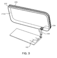
- FIG. 3 is a cross-sectional view schematically showing a second exemplary embodiment of an electrical connection shape between an antenna pattern frame and a circuit substrate;
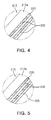
- FIG. 4 is a partially enlarged perspective view showing a first exemplary embodiment of "A" of FIG. 1 ;
- FIG. 5 is a partially enlarged perspective view showing a second exemplary embodiment of "A" of FIG. 1 ;
- FIG. 6 is a cross-sectional view of a first exemplary embodiment taken along line VI-VI of FIG. 1 ;
- FIG. 7 is a cross-sectional view of a second exemplary embodiment taken along line VI-VI of FIG. 1 ;
- FIG. 8 is a cross-sectional view of a third exemplary embodiment taken along line VI-VI of FIG. 1 ;
- FIG. 9 is a perspective view schematically showing a first exemplary embodiment of an interconnection part of the antenna pattern frame according to the exemplary embodiment of the present invention.
- FIG. 10 is a perspective view schematically showing a second exemplary embodiment of an interconnection part of the antenna pattern frame according to the exemplary embodiment of the present invention.
- FIG. 11 is a perspective view schematically showing a shape in which the wire antenna is wound on the antenna pattern frame
- FIG. 12 is a cross-sectional view showing a shape in which the antenna pattern frame according to the exemplary embodiment of the present invention is disposed in a manufacturing mold of an electronic device.
- FIG. 13 is a cross-sectional view schematically showing a shape that the antenna pattern frame according to the exemplary embodiment of the present invention is injection-molded in the manufacturing mold of an electronic device.
- FIG. 1 is an exploded perspective view of a case of an electronic device according to an exemplary embodiment of the present invention, a mobile communication terminal
- FIG. 2 is a cross-sectional view schematically showing a first exemplary embodiment of an electrical connection shape between an antenna pattern frame and a circuit substrate
- FIG. 3 is a cross-sectional view schematically showing a second exemplary embodiment of an electrical connection shape between an antenna pattern frame and a circuit substrate.
- an antenna pattern frame 200 provided with an antenna pattern part 222 forming wire antennas 220 is fixed into a case 120 of an electronic device, a mobile communication terminal 100 according to an exemplary embodiment of the present invention, such that it can be appreciated that the wire antennas 220 are embedded in the case 120 of the mobile communication terminal.
- the mobile communication terminal 100 that is one example of the electronic device may include the antenna pattern frame 200, a case frame 130, and a circuit substrate 140.
- the antenna pattern frame 200 may be fixed into the case frame 130 of the mobile communication terminal. Further, as will be described in detail below, the antenna pattern frame 200 is injection-molded by an electronic device manufacturing mold 400, such that it may be integrated with the case frame 130.
- the circuit substrate 140 is mounted with circuit elements that transmit and receive signals to and from the wire antennas 220.
- the circuit substrate 140 is provided with connection wirings connected to an interconnection part 224 of the antenna pattern frame 200.
- connection of the interconnection part 224 between the circuit substrate 140 and the antenna pattern frame 220 may be made by a C-clip 149 provided in the circuit substrate 140 as shown in FIG. 2 .
- the circuit substrate 140 may be connected to the antenna pattern frame 220 by a coaxial cable 149 provided in the connection part of the circuit substrate 140.
- the mobile communication terminal 100 that is the electronic device according to the exemplary embodiment of the present invention may include all the technical features of the antenna pattern frame 200 to be described below.
- the antenna pattern frame 200 may include a radiator frame 210 and the wire antennas 220.
- the radiator frame 210 is a plastic injection molded part.
- An insertion groove 212 may be formed on one surface 210a of the radiator frame 210 and a through part 214 connected from one point of the insertion groove 212 to an opposite surface 210b to the one surface 210a of the radiator frame 210 may be formed on the radiator frame 210.
- the wire antenna 220 is a wire made of a conductive material.
- the radiator frame 210 may include the wire antenna 220 that includes the antenna pattern part 222 formed to be inserted into the insertion groove 212 and the interconnection part 224 formed to be exposed to the opposite surface 210b by extending from the antenna pattern part 222 and penetrating through the through part 214.
- the wire antennas 220 may be lengthily formed to be appropriate to receive, in particular, broadcasting frequency bands that are a low frequency band.
- the insertion groove 212 formed in the radiator frame 210 may be formed on the side surface, the upper surface or the side surface and upper surface of the radiator frame 210.
- the insertion groove 212 may be formed over the radiator frame 210 so that the wire antenna 220 is a roof antenna by being wound on the edges of the radiator frame 210.
- FIG. 4 is a partially enlarged perspective view showing a first exemplary embodiment of "A" of FIG. 1
- FIG. 5 is a partially enlarged perspective view showing a second exemplary embodiment of "A" of FIG. 1 .
- FIG. 4 shows a shape where the wire antenna 220 is continuously wound on the insertion groove 212 to be lengthily formed and
- FIG. 5 shows a case where the plurality of wire antennas 220 are wound on the insertion groove 212 to receive a plurality of frequency band.
- the exemplary embodiment of FIG. 5 may form a cutting part 225 by forming the antenna pattern part 222 with one wire and then punching it.
- FIG. 6 is a cross-sectional view of a first exemplary embodiment taken along line VI-VI of FIG. 1
- FIG. 7 is a cross-sectional view of a second exemplary embodiment taken along line VI-VI of FIG. 1
- FIG. 8 is a cross-sectional view of a third exemplary embodiment taken along line VI-VI of FIG. 1 .
- FIG. 6 shows the embodiment in which the insertion groove 212 is formed to have the same depth as the diameter and thickness of the wire antenna 220 so as to expose the wire antenna to the outside.
- the expression "thickness" was used herein.
- FIG. 7 shows the structure where a coating part 230 is formed on the one surface 210a of the radiator frame 220 in order to increase adhesion between the wire antenna 220 and the radiator frame after winding the wire antenna 220 on the insertion groove 212.
- the coating part 230 may be formed on a portion of the one surface 210a or over the one surface 210a and may also be formed on the opposite surface 210b.
- FIG. 8 shows the case where the insertion groove 212 may be formed to have a depth larger than the diameter or the thickness of the wire antenna 220 and the wire antenna 220 may be more firmly fixed by thermal-bonding the insertion groove 212
- Reference numeral 260 shows the case where the insertion groove 212 is embedded by the thermal bonding.
- the thermal bonding process can smooth the surface of the antenna pattern frame 200 to increase the flowability of the injected liquid in the case that the case frame 130 is injection-molded.
- FIG. 9 is a perspective view schematically showing a first exemplary embodiment of an interconnection part of the antenna pattern frame according to the exemplary embodiment of the present invention
- FIG. 10 is a perspective view schematically showing a second exemplary embodiment of an interconnection part of the antenna pattern frame according to the exemplary embodiment of the present invention.
- FIGS. 9 and 10 show the shape where the interconnection part 224 of the antenna pattern frame 220 is formed.
- FIG. 9 shows the case where the interconnection part 224 may include an end 2242 of an interconnection pin formed to be bent at the opposite surface 210b.
- the interconnection part 224 is formed to be bent and thus may have tension, such that it may be easily connected with the circuit substrate 140. Further, the end 2242 of the interconnection part may be fixed to an end connection groove 2102 that is formed on the opposite surface 210b of the radiator frame 210.
- FIG. 10 shows a case where the interconnection part 224 may be exposed to the opposite surface 210b of the radiator frame 210 in a spiral shape.
- the structure of the interconnection part 224 according to the exemplary embodiment may stably contact the circuit substrate 140 by expanding the contact range therebetween.
- FIG. 11 is a perspective view schematically showing a shape in which the wire antenna is wound on the antenna pattern frame
- FIG. 12 is a cross-sectional view showing a shape in which the antenna pattern frame according to the exemplary embodiment of the present invention is disposed in a manufacturing mold of an electronic device
- FIG. 13 is a cross-sectional view schematically showing a shape in which the antenna pattern frame according to the exemplary embodiment of the present invention is injection-molded in the manufacturing mold of an electronic device.
- the insertion groove 212 in which the wire antenna 220 is inserted is formed on the one surface 210a of the radiator frame 210.
- the wire antenna 220 is inserted into the through hole 214 formed at one point of the inserting groove 212 and thus, is fixed to the opposite surface 210b of the radiator frame 210.
- the wire antenna 220 is inserted into the insertion groove 212 to form the antenna pattern frame 200.
- the number of wire antennas 220 may be provided as needed in the state where it is wound on a winding machine 300.
- the manufactured antenna pattern frame 200 may be disposed in the manufacturing mold 400 having an inner space 450 of the case shape of the electronic device to be injection-molded.
- the one surface 210a of the antenna pattern frame 200 is directed to the inner space 450, such that the wire antenna 220 may be embedded in the case frame 130 of the electronic device.
- the one surface of the antenna pattern frame 200 is surface-coated or thermal-bonded, thereby making it possible to improve the flowability of resin when performing the injection molding.
- the interconnection part 224 may be formed on the opposite surface of the antenna pattern frame 200 and the process of forming the interconnection part 224 may be performed in any process among the manufacturing processes, such as when the wire antenna 220 is fixed to the insertion groove 212 or after the injection molding is performed, or the like.
- the interconnection part 224 When the interconnection part 224 is formed, it may be electrically connected to the connection part of the circuit substrate 140 by a C-clip or a coaxial cable, or the like.
- the wire antenna is fixed to the radiator frame, thereby making it possible to simplify the manufacturing process and reduce the wasted amount of radiator to save manufacturing costs.
- the present invention can easily secure the length of the radiator to receive the signals of the low frequency band and can greatly simplify the manufacturing process, since there is no need to dispose the wire antenna in a separate mold and perform the injection molding thereon.
Landscapes
- Engineering & Computer Science (AREA)
- Computer Networks & Wireless Communication (AREA)
- Details Of Aerials (AREA)
- Support Of Aerials (AREA)
Abstract
Description
- This application claims the priority of Korean Patent Application No.
10-2010-0014298 filed on February 17, 2010 - The present invention relates to an antenna pattern part formed of a conductive wire, an electronic device provided with the antenna pattern frame, and a method for manufacturing the electronic device.
- Electronic devices such as mobile communication terminals, for example, cellular phones, PDAs, navigation devices, notebook computers, or the like, are necessities in modern society. The mobile communication terminals are being developed to have functions, such as CDMA, wireless LAN, GSM, DMB, or the like. One of the most important parts that enable the above functions is an antenna.
- The antenna currently used in a mobile communication terminal has evolved from an exterior type antenna such as a rod antenna or a helical antenna to an interior type antenna wherein an antenna is mounted in the terminal.
- There have been problems in that the exterior type is vulnerable to external impact and the interior type increases the volume of the terminal.
- In order to solve the problems, research to integrate the electronic device, i . e. , the mobile communication terminal and the antenna has been actively conducted.
- Recently, the applicant has proposed a method that forms an antenna pattern frame by performing injection molding on a radiator in order to embed an antenna in a case of an electronic device and embeds the radiator formed on the surface of the antenna pattern frame into the case of the electronic device by performing injection molding, i.e., double injection molding on the antenna pattern frame.
- In the above-mentioned antenna, since the antenna pattern is formed by pressing a metal plate, a radiator, there have been problems in that the length of the antenna pattern is long and the wasted amount of the antenna pattern is increased with the increase in the area of the antenna pattern to increase the material cost.
- Further, when the injection molding is performed in order to form the antenna pattern frame having an antenna pattern part formed on the surface thereof, it is very important to dispose the antenna pattern part in a manufacturing mold of the antenna pattern frame at the time of determining how accurately the antenna pattern part is disposed the case of the electronic device.
- In the case of an antenna for a low frequency band, a wavelength is long and thus, the length of the antenna becomes long. There has been a problem in that as the length of the antenna pattern becomes long, the structure of the manufacturing mold to fix the antenna pattern is complicated.
- An aspect of the present invention provides an antenna pattern frame capable of fixing a wire antenna to an injection molded part without using an injection molding method to fix a radiator to a manufacturing mold.
- Another aspect of the present invention provides an electronic device having a wire antenna embedded therein by using an antenna pattern frame to which the wire antenna is fixed.
- Still another aspect of the present invention provides a method for manufacturing an electronic device having a wire antenna embedded therein by using an antenna pattern frame to which the wire antenna is fixed.
- According to an aspect of the present invention, there is provided an antenna pattern frame, including: a radiator frame that has an insertion groove formed on one surface of the radiator frame and is provided with a through part connected from one point of the insertion groove to an opposite surface to the one surface of the radiator frame; and a wire antenna that includes an antenna pattern part formed to be inserted into the insertion groove and an interconnection part formed to be exposed to the opposite surface by extending from the antenna pattern part and penetrating through the through part.
- The insertion groove may be formed at the same depth as the diameter or thickness of the wire antenna.
- The insertion groove may be formed to have a depth larger than the diameter or thickness of the wire antenna.
- The antenna pattern frame may further include a coating part formed on the one surface of the radiator frame in order to increase the adhesion between the wire antenna and the radiator frame.
- The insertion groove may be surface-treated by thermal bonding.
- The insertion groove may be formed on the side surface, the upper surface, or the side surface and the upper surface of the radiator frame.
- The insertion groove may be formed on the radiator frame so that the wire antenna is a roof antenna.
- The wire antenna may be separated in plural.
- The interconnection part may include an end of an interconnection pin formed to be bent at the opposite surface and the opposite surface of the radiator frame may be provided with an end connection groove to which the end of the interconnection part is fixed.
- The interconnection part may be exposed at the opposite surface in a spiral shape.
- According to another aspect of the present invention, there is provided an electronic device, including: an antenna pattern frame that has an insertion groove formed on one surface of the antenna pattern frame and is provided with an interconnection part formed on an opposite surface to the one surface, a wire antenna being inserted into the insertion groove and the wire antenna being formed to penetrate through the interconnection part; a case frame of the electronic device formed so that the wire antenna is embedded between the case frame and the antenna pattern frame; and a circuit substrate that is electrically connected to the interconnection part to transmit and receive signals to and from the wire antenna.
- The case frame of the electronic device is formed on the one surface of the antenna pattern frame by injection molding.
- The one surface of the radiator frame may be formed with a coating part in order to increase the adhesion of the wire antenna in the insertion groove.
- The insertion groove may be formed to have a depth larger than the diameter or thickness of the wire antenna and the insertion groove may be subjected to thermal bonding to perform a surface treatment on the radiator frame.
- The insertion groove may be formed on the side surface, the upper surface, or the side surface and upper surface of the radiator frame.
- The insertion groove may be formed on the radiator frame so that the wire antenna is a roof antenna.
- The wire antenna may be separated in plural.
- The interconnection part may include an end of an interconnection pin formed to be bent at the opposite surface and the opposite surface of the radiator frame may be provided with an end connection groove to which the end of the interconnection part is fixed.
- The interconnection part may be connected to the circuit substrate by any one of a C-clip and a coaxial cable.
- The interconnection part may be exposed at the opposite surface in a spiral shape.
- The interconnection part may be connected to the circuit substrate by any one of a C-clip and a coaxial cable.
- According to another aspect of the present invention, there is provided a method for manufacturing an electronic device, including: forming an insertion groove into which a wire antenna is inserted on one surface of a radiator frame; inserting the wire antenna into a through hole formed at one point of the insertion groove to fix the wire antenna to the opposite surface of the radiator frame; forming an antenna pattern frame by inserting the wire antenna into the insertion groove; and injection-molding the antenna pattern frame by disposing the antenna pattern frame in a manufacturing mold having an inner space in a case shape of the electronic device.
- The method for manufacturing an electronic device may further include coating the one surface of the radiator frame in order to increase the adhesion of the wire antenna in the insertion groove.
- The insertion groove may be formed to have a depth larger than the diameter or thickness of the wire antenna and the insertion groove may be subjected to thermal bonding to perform a surface treatment on the radiator frame.
- The insertion groove may be formed on the side surface, the upper surface, or the side surface and upper surface of the radiator frame.
- The insertion groove may be formed on the radiator frame so that the wire antenna is a roof antenna.
- The wire antenna may be cut to be separated in plural.
- The method for manufacturing an electronic device may further include the interconnection part by bending the wire antenna at the opposite surface and fixing the interconnection part to the end connection groove on the opposite surface of the radiator frame.
- The interconnection part may be connected to the circuit substrate by any one of a C-clip and a coaxial cable.
- The method for manufacturing an electronic device may further include forming the interconnection part to expose the wire antenna at the opposite surface in a spiral shape.
- The interconnection part may be connected to the circuit substrate by any one of a C-clip and a coaxial cable.
- The above and other aspects, features and other advantages of the present invention will be more clearly understood from the following detailed description taken in conjunction with the accompanying drawings, in which:
-
FIG. 1 is an exploded perspective view of a case of an electronic device according to an exemplary of the present invention, a mobile communication terminal; -
FIG. 2 is a cross-sectional view schematically showing a first exemplary embodiment of an electrical connection shape between an antenna pattern frame and a circuit substrate; -
FIG. 3 is a cross-sectional view schematically showing a second exemplary embodiment of an electrical connection shape between an antenna pattern frame and a circuit substrate; -
FIG. 4 is a partially enlarged perspective view showing a first exemplary embodiment of "A" ofFIG. 1 ; -
FIG. 5 is a partially enlarged perspective view showing a second exemplary embodiment of "A" ofFIG. 1 ; -
FIG. 6 is a cross-sectional view of a first exemplary embodiment taken along line VI-VI ofFIG. 1 ; -
FIG. 7 is a cross-sectional view of a second exemplary embodiment taken along line VI-VI ofFIG. 1 ; -
FIG. 8 is a cross-sectional view of a third exemplary embodiment taken along line VI-VI ofFIG. 1 ; -
FIG. 9 is a perspective view schematically showing a first exemplary embodiment of an interconnection part of the antenna pattern frame according to the exemplary embodiment of the present invention; -
FIG. 10 is a perspective view schematically showing a second exemplary embodiment of an interconnection part of the antenna pattern frame according to the exemplary embodiment of the present invention; -
FIG. 11 is a perspective view schematically showing a shape in which the wire antenna is wound on the antenna pattern frame; -
FIG. 12 is a cross-sectional view showing a shape in which the antenna pattern frame according to the exemplary embodiment of the present invention is disposed in a manufacturing mold of an electronic device; and -
FIG. 13 is a cross-sectional view schematically showing a shape that the antenna pattern frame according to the exemplary embodiment of the present invention is injection-molded in the manufacturing mold of an electronic device. - Exemplary embodiments of the present invention will now be described in detail with reference to the accompanying drawings. However, it should be noted that the spirit of the present invention is not limited to the embodiments set forth herein and those skilled in the art and understanding the present invention can easily accomplish retrogressive inventions or other embodiments included in the spirit of the present invention by the addition, modification, and removal of components within the same spirit, but those are to be construed as being included in the spirit of the present invention.
- Further, throughout the drawings, the same or similar reference numerals will be used to designate the same components or like components having the same functions in the scope of the similar idea.
-
FIG. 1 is an exploded perspective view of a case of an electronic device according to an exemplary embodiment of the present invention, a mobile communication terminal,FIG. 2 is a cross-sectional view schematically showing a first exemplary embodiment of an electrical connection shape between an antenna pattern frame and a circuit substrate, andFIG. 3 is a cross-sectional view schematically showing a second exemplary embodiment of an electrical connection shape between an antenna pattern frame and a circuit substrate. - Referring to
FIGS. 1 through 3 , anantenna pattern frame 200 provided with anantenna pattern part 222 formingwire antennas 220 is fixed into acase 120 of an electronic device, amobile communication terminal 100 according to an exemplary embodiment of the present invention, such that it can be appreciated that thewire antennas 220 are embedded in thecase 120 of the mobile communication terminal. - The
mobile communication terminal 100 that is one example of the electronic device may include theantenna pattern frame 200, acase frame 130, and acircuit substrate 140. - As shown in
FIG. 1 , theantenna pattern frame 200 may be fixed into thecase frame 130 of the mobile communication terminal. Further, as will be described in detail below, theantenna pattern frame 200 is injection-molded by an electronicdevice manufacturing mold 400, such that it may be integrated with thecase frame 130. - The
circuit substrate 140 is mounted with circuit elements that transmit and receive signals to and from thewire antennas 220. Thecircuit substrate 140 is provided with connection wirings connected to aninterconnection part 224 of theantenna pattern frame 200. - In this configuration, the connection of the
interconnection part 224 between thecircuit substrate 140 and theantenna pattern frame 220 may be made by a C-clip 149 provided in thecircuit substrate 140 as shown inFIG. 2 . However, as shown inFIG. 3 , thecircuit substrate 140 may be connected to theantenna pattern frame 220 by acoaxial cable 149 provided in the connection part of thecircuit substrate 140. - Meanwhile, the
mobile communication terminal 100 that is the electronic device according to the exemplary embodiment of the present invention may include all the technical features of theantenna pattern frame 200 to be described below. - The
antenna pattern frame 200 may include aradiator frame 210 and thewire antennas 220. - The
radiator frame 210 is a plastic injection molded part. Aninsertion groove 212 may be formed on onesurface 210a of theradiator frame 210 and a throughpart 214 connected from one point of theinsertion groove 212 to anopposite surface 210b to the onesurface 210a of theradiator frame 210 may be formed on theradiator frame 210. - The
wire antenna 220 is a wire made of a conductive material. Theradiator frame 210 may include thewire antenna 220 that includes theantenna pattern part 222 formed to be inserted into theinsertion groove 212 and theinterconnection part 224 formed to be exposed to theopposite surface 210b by extending from theantenna pattern part 222 and penetrating through the throughpart 214. - The
wire antennas 220 may be lengthily formed to be appropriate to receive, in particular, broadcasting frequency bands that are a low frequency band. In other words, theinsertion groove 212 formed in theradiator frame 210 may be formed on the side surface, the upper surface or the side surface and upper surface of theradiator frame 210. - At this time, the
insertion groove 212 may be formed over theradiator frame 210 so that thewire antenna 220 is a roof antenna by being wound on the edges of theradiator frame 210. -
FIG. 4 is a partially enlarged perspective view showing a first exemplary embodiment of "A" ofFIG. 1 andFIG. 5 is a partially enlarged perspective view showing a second exemplary embodiment of "A" ofFIG. 1 . -
FIG. 4 shows a shape where thewire antenna 220 is continuously wound on theinsertion groove 212 to be lengthily formed andFIG. 5 shows a case where the plurality ofwire antennas 220 are wound on theinsertion groove 212 to receive a plurality of frequency band. - At this time, the exemplary embodiment of
FIG. 5 may form a cuttingpart 225 by forming theantenna pattern part 222 with one wire and then punching it. -
FIG. 6 is a cross-sectional view of a first exemplary embodiment taken along line VI-VI ofFIG. 1 ,FIG. 7 is a cross-sectional view of a second exemplary embodiment taken along line VI-VI ofFIG. 1 , andFIG. 8 is a cross-sectional view of a third exemplary embodiment taken along line VI-VI ofFIG. 1 . -
FIG. 6 shows the embodiment in which theinsertion groove 212 is formed to have the same depth as the diameter and thickness of thewire antenna 220 so as to expose the wire antenna to the outside. - Since the
wire antenna 220 is not necessarily a circular shape, the expression "thickness" was used herein. -
FIG. 7 shows the structure where acoating part 230 is formed on the onesurface 210a of theradiator frame 220 in order to increase adhesion between thewire antenna 220 and the radiator frame after winding thewire antenna 220 on theinsertion groove 212. - The
coating part 230 may be formed on a portion of the onesurface 210a or over the onesurface 210a and may also be formed on theopposite surface 210b. -
FIG. 8 shows the case where theinsertion groove 212 may be formed to have a depth larger than the diameter or the thickness of thewire antenna 220 and thewire antenna 220 may be more firmly fixed by thermal-bonding theinsertion groove 212 Reference numeral 260 shows the case where theinsertion groove 212 is embedded by the thermal bonding. - The thermal bonding process can smooth the surface of the
antenna pattern frame 200 to increase the flowability of the injected liquid in the case that thecase frame 130 is injection-molded. -
FIG. 9 is a perspective view schematically showing a first exemplary embodiment of an interconnection part of the antenna pattern frame according to the exemplary embodiment of the present invention, andFIG. 10 is a perspective view schematically showing a second exemplary embodiment of an interconnection part of the antenna pattern frame according to the exemplary embodiment of the present invention. -
FIGS. 9 and 10 show the shape where theinterconnection part 224 of theantenna pattern frame 220 is formed. -
FIG. 9 shows the case where theinterconnection part 224 may include anend 2242 of an interconnection pin formed to be bent at theopposite surface 210b. Theinterconnection part 224 is formed to be bent and thus may have tension, such that it may be easily connected with thecircuit substrate 140. Further, theend 2242 of the interconnection part may be fixed to anend connection groove 2102 that is formed on theopposite surface 210b of theradiator frame 210. -
FIG. 10 shows a case where theinterconnection part 224 may be exposed to theopposite surface 210b of theradiator frame 210 in a spiral shape. The structure of theinterconnection part 224 according to the exemplary embodiment may stably contact thecircuit substrate 140 by expanding the contact range therebetween. -
FIG. 11 is a perspective view schematically showing a shape in which the wire antenna is wound on the antenna pattern frame,FIG. 12 is a cross-sectional view showing a shape in which the antenna pattern frame according to the exemplary embodiment of the present invention is disposed in a manufacturing mold of an electronic device, andFIG. 13 is a cross-sectional view schematically showing a shape in which the antenna pattern frame according to the exemplary embodiment of the present invention is injection-molded in the manufacturing mold of an electronic device. - First, the
insertion groove 212 in which thewire antenna 220 is inserted is formed on the onesurface 210a of theradiator frame 210. Thewire antenna 220 is inserted into the throughhole 214 formed at one point of the insertinggroove 212 and thus, is fixed to theopposite surface 210b of theradiator frame 210. - If one end of the
wire antenna 220 is fixed to theradiator frame 210, thewire antenna 220 is inserted into theinsertion groove 212 to form theantenna pattern frame 200. - At this time, the number of
wire antennas 220 may be provided as needed in the state where it is wound on a windingmachine 300. - The manufactured
antenna pattern frame 200 may be disposed in themanufacturing mold 400 having aninner space 450 of the case shape of the electronic device to be injection-molded. - The one
surface 210a of theantenna pattern frame 200 is directed to theinner space 450, such that thewire antenna 220 may be embedded in thecase frame 130 of the electronic device. - Meanwhile, the one surface of the
antenna pattern frame 200 is surface-coated or thermal-bonded, thereby making it possible to improve the flowability of resin when performing the injection molding. - Further, the
interconnection part 224 may be formed on the opposite surface of theantenna pattern frame 200 and the process of forming theinterconnection part 224 may be performed in any process among the manufacturing processes, such as when thewire antenna 220 is fixed to theinsertion groove 212 or after the injection molding is performed, or the like. - When the
interconnection part 224 is formed, it may be electrically connected to the connection part of thecircuit substrate 140 by a C-clip or a coaxial cable, or the like. - As set forth above, according to the antenna pattern frame, the electronic device provided with the antenna pattern frame, and the method for manufacturing the electronic device of the present invention, the wire antenna is fixed to the radiator frame, thereby making it possible to simplify the manufacturing process and reduce the wasted amount of radiator to save manufacturing costs.
- Further, the present invention can easily secure the length of the radiator to receive the signals of the low frequency band and can greatly simplify the manufacturing process, since there is no need to dispose the wire antenna in a separate mold and perform the injection molding thereon.
- While the present invention has been shown and described in connection with the exemplary embodiments, it will be apparent to those skilled in the art that modifications and variations can be made without departing from the spirit and scope of the invention as defined by the appended claims.
Claims (31)
- An antenna pattern frame, comprising:a radiator frame that has an insertion groove formed on one surface of the radiator frame and is provided with a through part connected from one point of the insertion groove to an opposite surface to the one surface of the radiator frame; anda wire antenna that includes an antenna pattern part formed to be inserted into the insertion groove and an interconnection part formed to be exposed to the opposite surface by extending from the antenna pattern part and penetrating through the through part.
- The antenna pattern frame of claim 1, wherein the insertion groove is formed at the same depth as the diameter or thickness of the wire antenna.
- The antenna pattern frame of claim 1, wherein the insertion groove is formed to have a depth larger than the diameter or thickness of the wire antenna
- The antenna pattern frame of claim 1, further comprising a coating part formed on the one surface of the radiator frame in order to increase the adhesion between the wire antenna and the radiator frame.
- The antenna pattern frame of claim 1, wherein the insertion groove is surface-treated by thermal bonding.
- The antenna pattern frame of claim 1, wherein the insertion groove is formed on the side surface, the upper surface, or the side surface and the upper surface of the radiator frame.
- The antenna pattern frame of claim 1, wherein the insertion groove is formed on the radiator frame so that the wire antenna is a roof antenna.
- The antenna pattern frame of claim 1, wherein the wire antenna is separated in plural.
- The antenna pattern frame of claim 1, wherein the interconnection part includes an end of an interconnection pin formed to be bent at the opposite surface and the opposite surface of the radiator frame is provided with an end connection groove to which the end of the interconnection part is fixed.
- The antenna pattern frame of claim 1, wherein the interconnection part is exposed at the opposite surface in a spiral shape.
- An electronic device, comprising:an antenna pattern frame that has an insertion groove formed on one surface of the antenna pattern frame and is provided with an interconnection part formed on an opposite surface to the one surface, a wire antenna being inserted into the insertion groove and the wire antenna being formed to penetrate through the interconnection part;a case frame formed so that the wire antenna is embedded between the case frame and the antenna pattern frame; anda circuit substrate that is electrically connected to the interconnection part to transmit and receive signals to and from the wire antenna.
- The electronic device of claim 11, wherein the case frame is formed on the one surface of the antenna pattern frame by injection molding.
- The electronic device of claim 11, wherein the one surface of the radiator frame is formed with a coating part in order to increase the adhesion of the wire antenna in the insertion groove.
- The electronic device of claim 11, wherein the insertion groove is formed to have a depth larger than the diameter or thickness of the wire antenna and the insertion groove is subjected to thermal bonding to perform a surface treatment on the radiator frame.
- The electronic device of claim 11, wherein the insertion groove is formed on the side surface, the upper surface, or the side surface and upper surface of the radiator frame.
- The electronic device of claim 11, wherein the insertion groove is formed on the radiator frame so that the wire antenna is a roof antenna.
- The electronic device of claim 11, wherein the wire antenna is separated in plural.
- The electronic device of claim 11, wherein the interconnection part includes an end of an interconnection pin formed to be bent at the opposite surface and the opposite surface of the radiator frame is provided with an end connection groove to which the end of the interconnection part is fixed.
- The electronic device of claim 18, wherein the interconnection part is connected to the circuit substrate by any one of a C-clip and a coaxial cable.
- The electronic device of claim 11, wherein the interconnection part is exposed at the opposite surface in a spiral shape.
- The electronic device of claim 20, wherein the interconnection part is connected to the circuit substrate by any one of a C-clip and a coaxial cable.
- A method for manufacturing an electronic device, comprising:forming an insertion groove into which a wire antenna is inserted on one surface of a radiator frame;inserting the wire antenna into a through hole formed at one point of the insertion groove to fix the wire antenna to the opposite surface of the radiator frame;forming an antenna pattern frame by inserting the wire antenna into the insertion groove; andinjection-molding the antenna pattern frame by disposing the antenna pattern frame in a manufacturing mold having an inner space in a case shape of the electronic device.
- The method for manufacturing an electronic device of claim 22, further comprising coating the one surface of the radiator frame in order to increase the adhesion of the wire antenna in the insertion groove.
- The method for manufacturing an electronic device of claim 22, wherein the insertion groove is formed to have a depth larger than the diameter or thickness of the wire antenna and the insertion groove is subjected to thermal bonding to perform a surface treatment on the radiator frame.
- The method for manufacturing an electronic device of claim 22, wherein the insertion groove is formed on the side surface, the upper surface, or the side surface and upper surface of the radiator frame.
- The method for manufacturing an electronic device of claim 22, wherein the insertion groove is formed on the radiator frame so that the wire antenna is a roof antenna.
- The method for manufacturing an electronic device of claim 22, wherein the wire antenna is cut to be separated in plural.
- The method for manufacturing an electronic device of claim 22, further comprising forming the interconnection part by bending the wire antenna at the opposite surface and fixing the interconnection part to the end connection groove on the opposite surface of the radiator frame.
- The method for manufacturing an electronic device of claim 28, wherein the interconnection part is connected to the circuit substrate by any one of a C-clip and a coaxial cable.
- The method for manufacturing an electronic device of claim 22, further comprising forming the interconnection part to expose the wire antenna at the opposite surface in a spiral shape.
- The method for manufacturing an electronic device of claim 30, wherein the interconnection part is connected to the circuit substrate by any one of a C-clip and a coaxial cable.
Applications Claiming Priority (1)
| Application Number | Priority Date | Filing Date | Title |
|---|---|---|---|
| KR1020100014298A KR101101649B1 (en) | 2010-02-17 | 2010-02-17 | An electronic device having an antenna pattern frame and an antenna pattern frame, and a method of manufacturing the same |
Publications (1)
| Publication Number | Publication Date |
|---|---|
| EP2360784A1 true EP2360784A1 (en) | 2011-08-24 |
Family
ID=43971195
Family Applications (1)
| Application Number | Title | Priority Date | Filing Date |
|---|---|---|---|
| EP11250177A Withdrawn EP2360784A1 (en) | 2010-02-17 | 2011-02-16 | Antenna pattern frame, electronic device provided with antenne pattern frame and method for manufacturing electronic device |
Country Status (5)
| Country | Link |
|---|---|
| US (1) | US20110199269A1 (en) |
| EP (1) | EP2360784A1 (en) |
| JP (1) | JP2011172222A (en) |
| KR (1) | KR101101649B1 (en) |
| CN (1) | CN102163762A (en) |
Cited By (1)
| Publication number | Priority date | Publication date | Assignee | Title |
|---|---|---|---|---|
| US9944777B2 (en) | 2013-05-13 | 2018-04-17 | Compagnie Generale Des Etablissements Michelin | Rubber composition with high processability for run-flat tire |
Families Citing this family (5)
| Publication number | Priority date | Publication date | Assignee | Title |
|---|---|---|---|---|
| JP2012222701A (en) * | 2011-04-12 | 2012-11-12 | Panasonic Corp | Portable radio device |
| EP2709205A1 (en) * | 2012-09-13 | 2014-03-19 | LG Innotek Co., Ltd. | Antenna apparatus and method of manufacturing the same |
| KR102006489B1 (en) * | 2012-12-26 | 2019-08-01 | 엘지전자 주식회사 | Mobile terminal and method for producting of the same |
| KR101634285B1 (en) * | 2015-02-02 | 2016-06-30 | 주식회사 알.에프.텍 | Smart phone case with antenna and method of manufacturing the same |
| US20230085660A1 (en) * | 2021-09-17 | 2023-03-23 | Zebra Technologies Corporation | Mobile Device Housing with Integrated Antenna Carrier |
Citations (7)
| Publication number | Priority date | Publication date | Assignee | Title |
|---|---|---|---|---|
| US4894663A (en) * | 1987-11-16 | 1990-01-16 | Motorola, Inc. | Ultra thin radio housing with integral antenna |
| EP1635419A1 (en) * | 2004-09-13 | 2006-03-15 | Nec Corporation | Antenna and radio communication terminal having antenna |
| US20070241971A1 (en) * | 2006-04-13 | 2007-10-18 | Kabushiki Kaisha Toshiba | Mobile communication terminal |
| US20080182539A1 (en) * | 2007-01-25 | 2008-07-31 | Yoshikazu Hata | Electronic apparatus |
| WO2008143452A1 (en) * | 2007-05-21 | 2008-11-27 | E.M.W. Antenna Co., Ltd. | Wireless device exterior case antenna |
| US20090082075A1 (en) * | 2007-09-25 | 2009-03-26 | Tomoko Honda | Casing and method for manufacturing same, and electronic device |
| KR100932079B1 (en) * | 2009-03-31 | 2009-12-15 | 마상영 | Insert antenna module for portable terminal and manufacturing method thereof |
Family Cites Families (9)
| Publication number | Priority date | Publication date | Assignee | Title |
|---|---|---|---|---|
| JPS5118142B1 (en) * | 1970-09-21 | 1976-06-08 | ||
| JPH0540960U (en) * | 1991-10-25 | 1993-06-01 | シチズン時計株式会社 | Data carrier structure |
| GB2345196B (en) * | 1998-12-23 | 2003-11-26 | Nokia Mobile Phones Ltd | An antenna and method of production |
| KR20040000268A (en) * | 2002-06-24 | 2004-01-03 | 엘지전자 주식회사 | Loop antenna |
| JP4539038B2 (en) * | 2003-06-30 | 2010-09-08 | ソニー株式会社 | Data communication device |
| JP2006279161A (en) * | 2005-03-28 | 2006-10-12 | Mitsumi Electric Co Ltd | Antenna device and antenna element |
| KR20080061274A (en) * | 2006-12-27 | 2008-07-02 | 가부시키가이샤 한도오따이 에네루기 켄큐쇼 | Antenna and semiconductor device having the antenna |
| JP2008205680A (en) * | 2007-02-19 | 2008-09-04 | Matsushita Electric Ind Co Ltd | ANTENNA DEVICE AND ELECTRONIC DEVICE USING THE SAME |
| US7530823B1 (en) * | 2008-01-07 | 2009-05-12 | Sony Ericsson Mobile Communications Ab | USB modem devices with a flip antenna and a retractable USB connector |
-
2010
- 2010-02-17 KR KR1020100014298A patent/KR101101649B1/en not_active Expired - Fee Related
-
2011
- 2011-02-08 US US13/023,125 patent/US20110199269A1/en not_active Abandoned
- 2011-02-10 JP JP2011027663A patent/JP2011172222A/en active Pending
- 2011-02-16 EP EP11250177A patent/EP2360784A1/en not_active Withdrawn
- 2011-02-17 CN CN2011100411611A patent/CN102163762A/en active Pending
Patent Citations (7)
| Publication number | Priority date | Publication date | Assignee | Title |
|---|---|---|---|---|
| US4894663A (en) * | 1987-11-16 | 1990-01-16 | Motorola, Inc. | Ultra thin radio housing with integral antenna |
| EP1635419A1 (en) * | 2004-09-13 | 2006-03-15 | Nec Corporation | Antenna and radio communication terminal having antenna |
| US20070241971A1 (en) * | 2006-04-13 | 2007-10-18 | Kabushiki Kaisha Toshiba | Mobile communication terminal |
| US20080182539A1 (en) * | 2007-01-25 | 2008-07-31 | Yoshikazu Hata | Electronic apparatus |
| WO2008143452A1 (en) * | 2007-05-21 | 2008-11-27 | E.M.W. Antenna Co., Ltd. | Wireless device exterior case antenna |
| US20090082075A1 (en) * | 2007-09-25 | 2009-03-26 | Tomoko Honda | Casing and method for manufacturing same, and electronic device |
| KR100932079B1 (en) * | 2009-03-31 | 2009-12-15 | 마상영 | Insert antenna module for portable terminal and manufacturing method thereof |
Cited By (1)
| Publication number | Priority date | Publication date | Assignee | Title |
|---|---|---|---|---|
| US9944777B2 (en) | 2013-05-13 | 2018-04-17 | Compagnie Generale Des Etablissements Michelin | Rubber composition with high processability for run-flat tire |
Also Published As
| Publication number | Publication date |
|---|---|
| US20110199269A1 (en) | 2011-08-18 |
| KR101101649B1 (en) | 2012-01-02 |
| CN102163762A (en) | 2011-08-24 |
| KR20110094725A (en) | 2011-08-24 |
| JP2011172222A (en) | 2011-09-01 |
Similar Documents
| Publication | Publication Date | Title |
|---|---|---|
| KR100944932B1 (en) | Antenna embeded mobile communication terminal case and method of manufacturing the same, mobile communication terminal | |
| US9419326B2 (en) | Antenna pattern frame, method and mold for manufacturing the same, method for manufacturing an electronic device case, and electronic device | |
| US8711041B2 (en) | Case of electronic device having antenna pattern embedded therein and mold and method for manufacturing the same | |
| US8643547B2 (en) | Antenna pattern frame, method and mold for manufacturing the same, electronic device case having antenna pattern frame embedded therein, and method for manufacturing the same | |
| EP2361744A1 (en) | Antenna pattern frame and mold for manufacturing electronic device case including the same | |
| EP2403065A2 (en) | Electronic device case having antenna pattern embedded therein, method for manufacturing the same, mold for manufacturing antenna pattern frame, and electronic device | |
| US20110221639A1 (en) | Antenna pattern frame, case of electronic device and mold for manufacturing the same | |
| EP2390019A1 (en) | Antenna radiator, method of manufacturing electronic device case having plurality of antenna pattern radiators embedded therein, and electronic device case | |
| US20110199269A1 (en) | Antenna pattern frame, electronic device provided with antenna pattern frame and method for manufacturing electronic device | |
| US8933844B2 (en) | Antenna pattern frame, electronic device case provided with antenna pattern frame and electronic device including electronic device case | |
| EP2386400A1 (en) | Case of electronic device having antenna pattern frame embedded therein, mold therefor and method of manufacturing thereof | |
| US20100234082A1 (en) | Method of manufacturing case for mobile communications terminal, case for mobile communications terminal, and mobile communications terminal having the same | |
| CN104953237A (en) | Electronic device case, method for manufacturing the same, and mobile communications terminal | |
| US8976074B2 (en) | Case of electronic device having low frequency antenna pattern embedded therein, mold therefor and method of manufacturing thereof | |
| EP2367231A1 (en) | Electronic device case, mold for manufacturing the same, and mobile communications terminal | |
| EP2339694A1 (en) | Cable connection pin and embedded antenna type electronic device having the same | |
| KR20090121973A (en) | Film Antenna and Mobile Terminal | |
| KR101113346B1 (en) | method and mould for manufacturing case of electronic device having antenna radiation device embeded therein | |
| KR101123767B1 (en) | Protrusion structure for combining of internal antenna, internal antenna assembly comprising the structure, and method for manufacturing the same | |
| US20100035564A1 (en) | Mobile communication terminal case and mobile communication terminal | |
| KR101179362B1 (en) | Case of electronic device having antenna pattern for low frequency embeded therein, mould and method for manufacturing the same | |
| KR20090063939A (en) | Built-in antenna manufacturing method | |
| US20100330934A1 (en) | Combination module with antenna and audio-component | |
| JP2009177662A (en) | Antenna apparatus | |
| JP2009177661A (en) | Antenna device |
Legal Events
| Date | Code | Title | Description |
|---|---|---|---|
| PUAI | Public reference made under article 153(3) epc to a published international application that has entered the european phase |
Free format text: ORIGINAL CODE: 0009012 |
|
| 17P | Request for examination filed |
Effective date: 20110303 |
|
| AK | Designated contracting states |
Kind code of ref document: A1 Designated state(s): AL AT BE BG CH CY CZ DE DK EE ES FI FR GB GR HR HU IE IS IT LI LT LU LV MC MK MT NL NO PL PT RO RS SE SI SK SM TR |
|
| AX | Request for extension of the european patent |
Extension state: BA ME |
|
| RIN1 | Information on inventor provided before grant (corrected) |
Inventor name: AN, CHAN GWANG Inventor name: LEE, DAE KYU Inventor name: LEE, DUK WOO Inventor name: JEON, DAE SEONG Inventor name: MUN, HYUN SAM Inventor name: LEE, BYUNG HWA Inventor name: KIM, TAE SUNG Inventor name: CHO, SUNG EUN Inventor name: HONG, HA RYONG Inventor name: SUNG, JAE SUK |
|
| 17Q | First examination report despatched |
Effective date: 20120503 |
|
| STAA | Information on the status of an ep patent application or granted ep patent |
Free format text: STATUS: THE APPLICATION IS DEEMED TO BE WITHDRAWN |
|
| 18D | Application deemed to be withdrawn |
Effective date: 20140430 |