EP2360448A1 - Microelectromechanical gyroscope with calibrated synchronization of actuation and method for actuating a microelectromechanical gyroscope - Google Patents
Microelectromechanical gyroscope with calibrated synchronization of actuation and method for actuating a microelectromechanical gyroscope Download PDFInfo
- Publication number
- EP2360448A1 EP2360448A1 EP11154596A EP11154596A EP2360448A1 EP 2360448 A1 EP2360448 A1 EP 2360448A1 EP 11154596 A EP11154596 A EP 11154596A EP 11154596 A EP11154596 A EP 11154596A EP 2360448 A1 EP2360448 A1 EP 2360448A1
- Authority
- EP
- European Patent Office
- Prior art keywords
- driving
- clock signal
- frequency
- mass
- aux
- Prior art date
- Legal status (The legal status is an assumption and is not a legal conclusion. Google has not performed a legal analysis and makes no representation as to the accuracy of the status listed.)
- Granted
Links
Images


Classifications
-
- G—PHYSICS
- G01—MEASURING; TESTING
- G01C—MEASURING DISTANCES, LEVELS OR BEARINGS; SURVEYING; NAVIGATION; GYROSCOPIC INSTRUMENTS; PHOTOGRAMMETRY OR VIDEOGRAMMETRY
- G01C19/00—Gyroscopes; Turn-sensitive devices using vibrating masses; Turn-sensitive devices without moving masses; Measuring angular rate using gyroscopic effects
- G01C19/56—Turn-sensitive devices using vibrating masses, e.g. vibratory angular rate sensors based on Coriolis forces
-
- G—PHYSICS
- G01—MEASURING; TESTING
- G01C—MEASURING DISTANCES, LEVELS OR BEARINGS; SURVEYING; NAVIGATION; GYROSCOPIC INSTRUMENTS; PHOTOGRAMMETRY OR VIDEOGRAMMETRY
- G01C19/00—Gyroscopes; Turn-sensitive devices using vibrating masses; Turn-sensitive devices without moving masses; Measuring angular rate using gyroscopic effects
- G01C19/56—Turn-sensitive devices using vibrating masses, e.g. vibratory angular rate sensors based on Coriolis forces
- G01C19/5719—Turn-sensitive devices using vibrating masses, e.g. vibratory angular rate sensors based on Coriolis forces using planar vibrating masses driven in a translation vibration along an axis
- G01C19/5726—Signal processing
-
- G—PHYSICS
- G01—MEASURING; TESTING
- G01C—MEASURING DISTANCES, LEVELS OR BEARINGS; SURVEYING; NAVIGATION; GYROSCOPIC INSTRUMENTS; PHOTOGRAMMETRY OR VIDEOGRAMMETRY
- G01C19/00—Gyroscopes; Turn-sensitive devices using vibrating masses; Turn-sensitive devices without moving masses; Measuring angular rate using gyroscopic effects
- G01C19/56—Turn-sensitive devices using vibrating masses, e.g. vibratory angular rate sensors based on Coriolis forces
- G01C19/5719—Turn-sensitive devices using vibrating masses, e.g. vibratory angular rate sensors based on Coriolis forces using planar vibrating masses driven in a translation vibration along an axis
- G01C19/5733—Structural details or topology
- G01C19/5755—Structural details or topology the devices having a single sensing mass
- G01C19/5762—Structural details or topology the devices having a single sensing mass the sensing mass being connected to a driving mass, e.g. driving frames
Definitions
- the present invention relates to a microelectromechanical gyroscope with calibrated synchronization of actuation and to a method for actuating a microelectromechanical gyroscope.
- MEMS microelectromechanical systems
- MEMS of this type are usually based on microelectromechanical structures comprising at least one movable mass connected to a fixed body (stator) by springs and movable with respect to the stator according to pre-determined degrees of freedom.
- the movable mass is moreover coupled to the fixed body via capacitive structures (capacitors).
- Capacitors The movement of the movable mass with respect to the fixed body, for example on account of an external stress, modifies the capacitance of the capacitors; from this it is possible to trace back to the relative displacement of the movable mass with respect to the fixed body and hence to the force applied.
- by supplying appropriate biasing voltages it is possible to apply an electrostatic force to the movable mass to set it in motion.
- the frequency response of inertial MEMS structures is exploited, which is typically of the second-order low-pass type.
- MEMS in particular, all electromechanical oscillators and gyroscopes
- driving devices that have the task of maintaining the movable mass in oscillation.
- a first type of known solution envisages supplying, in open loop, periodic excitation at the resonance frequency of the MEMS structure.
- the solution is simple, but also far from effective, because the resonance frequency is not known with precision on account of the ineliminable dispersions in the processes of micromachining of semiconductors.
- the resonance frequency of each individual device can vary over time, for example, on account of temperature gradients or, more simply, on account of ageing.
- Feedback driving circuits have then been proposed, based upon the use of sigma-delta modulators. Circuits of this type are undoubtedly more effective than the previous ones in stabilizing the oscillation of the movable mass at the real resonance frequency and in suppressing disturbance. However, various stages are necessary for filtering, decimation, and further processing of the bitstream supplied by the sigma-delta modulator. For this reason, currently available feedback driving circuits are complex to produce, cumbersome and, in practice, costly.
- gyroscopes have a complex electromechanical structure, which comprises two masses that are movable with respect to the stator and are coupled to one another so as to present a relative degree of freedom.
- the two movable masses are both capacitively coupled to the stator.
- One of the movable masses is dedicated to driving (driving mass) and is kept in oscillation at the resonance frequency.
- the other movable mass (sensing mass) is driven in the oscillatory motion and, in the case of rotation of the microstructure with respect to a pre-determined axis with an angular velocity, is subject to a Coriolis force proportional to the angular velocity itself.
- the sensing mass operates as an accelerometer that enables sensing of the Coriolis acceleration.
- the driving mass is equipped with two types of differential capacitive structures: driving electrodes and driving-detection electrodes.
- the driving electrodes have the purpose of sustaining self-oscillation of the movable mass in the direction of actuation, through electrostatic forces generated by the spectral component of the noise at the mechanical resonance frequency of the driving mass.
- the driving-detection electrodes have the purpose of measuring, through the transduced charge, the position of translation or rotation of the sensing mass in the direction of actuation.
- the patent No. EP 1 624 285 describes a system for controlling the velocity of oscillation of the gyroscope, comprising a differential sense amplifier, a high-pass amplifier, and an actuation and control stage, operating in a continuous-time mode.
- control loop comprises a low-pass filter in order to reduce the offset and the effects of parasitic components and couplings by operating on the overall gain and phase of the feedback loop.
- phase-locked-loop (PLL) circuits are normally used, which have, however, a far from negligible impact in terms of area occupation, as well as of consumption levels, and require external filtering components for operating properly.
- the PLL circuits may require transients even of several hundreds of milliseconds before completing phase locking. The consequent delay in the response can be critical in certain applications.
- the aim of the present invention is to provide a microelectromechanical gyroscope and a method for actuating a microelectromechanical gyroscope that will make it possible to overcome the limitations described.
- a microelectromechanical gyroscope and a method for actuating a microelectromechanical gyroscope are provided, as claimed in Claim 1 and Claim 15, respectively.
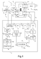
- Figure 1 shows as a whole a microelectromechanical gyroscope 1, which comprises a microstructure 2, made of semiconductor material, a driving device 3, a read generator 4, and a read device 5.
- the microstructure 2 is made of semiconductor material and comprises a fixed structure 6, a driving mass 7, and at least one sensing mass 8.
- a uniaxial gyroscope in which a single sensing mass 8 is present.
- What is described hereinafter applies, however, also to the case of multiaxial gyroscopes, which comprise two or more sensing masses or systems of sensing masses, for detecting rotations according to respective independent axes.
- the driving mass 7 is elastically constrained to the fixed structure 6 so as to be able to oscillate about a resting position according to a translational or rotational degree of freedom.
- the sensing mass 8 is mechanically coupled to the driving mass 7 so as to be driven in motion according to the degree of freedom of the driving mass 7 itself.
- the sensing mass 8 is elastically constrained to the driving mass 7 so as to oscillate in turn with respect to the driving mass 7 itself, with a respective further degree of freedom.
- the driving mass 7 is linearly movable along a driving axis X, while the sensing mass 8 is movable with respect to the driving mass 7 according to a sensing axis Y, that is perpendicular to the driving axis X.
- the type of movement (whether translational or rotational) allowed by the degrees of freedom and the arrangement of the driving and sensing axes may vary according to the type of gyroscope.
- the expression “according to an axis” will be indifferently used in relation to movements along an axis or about an axis, according to whether movements allowed to the masses by the respective degrees of freedom are translational (along an axis) or else rotational (about an axis).
- the expression “according to a degree of freedom” will be indifferently used in relation to translational or rotational movements, as allowed by the degree of freedom itself.
- the driving mass 7 (with the sensing mass 8) is connected to the fixed structure 6 so as to define a resonant mechanical system with a resonance frequency ⁇ R (according to the driving axis X) .
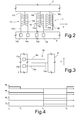
- the driving mass 7 ( Figure 2 ) is capacitively coupled to the fixed structure 6 through driving units 10 and feedback-sensing units 12.
- the capacitive coupling is of a differential type.
- the actuation units 10 comprise first and second fixed driving electrodes 10a, 10b, which are anchored to the fixed structure 6 and extend substantially perpendicular to the driving direction X, and movable driving electrodes 10c, which are anchored to the driving mass 7 and are also substantially perpendicular to the driving direction X.
- the movable driving electrodes 10c are comb-fingered and capacitively coupled with respective first fixed driving electrodes 10a and second fixed driving electrodes 10b.
- the first and second fixed driving electrodes 10a, 10b of the actuation units 10 are electrically connected to a first driving terminal 13a and to a second driving terminal 13b, respectively, of the microstructure 2.
- the coupling is of a differential type.
- each actuation unit 10 a movement of the driving mass 7 along the driving axis X causes the capacitance between the movable driving electrode 10c and one of the fixed driving electrodes 10a, 10b to increase.
- the capacitance between the movable driving electrode 10c and the other of the fixed driving electrodes 10a, 10b decreases instead accordingly.
- the structure of the feedback-sensing units 12 is similar to that of the actuation units 10.
- the feedback-sensing units 12 comprise first and second fixed sensing electrodes 12a, 12b, anchored to the fixed structure 6, and movable sensing electrodes 12c, anchored to the driving mass 7 and comb-fingered and capacitively coupled with respective first fixed sensing electrodes 12a and second fixed sensing electrodes 12b.
- the first and second fixed sensing electrodes 12a, 12b of the feedback-sensing units 12 are electrically connected respectively to a first feedback-sensing terminal 14a and a second feedback-sensing terminal 14b of the microstructure 2.
- the driving mass 7 is coupled to the driving terminals 13a, 13b through differential driving capacitances C D1 , C D2 and to the sensing terminals 14a, 14b through feedback-sensing differential capacitances C FBS1 , C FBS2 .
- the sensing mass 8 is electrically connected to the driving mass 7, without interposition of insulating structures. Consequently, the sensing mass 8 and the driving mass 7 are at the same potential.
- the sensing mass 8 is moreover capacitively coupled to the fixed structure 6 through signal-sensing units 15 ( Figure 3 ). More precisely, the signal-sensing units 15 comprise third and fourth fixed sensing electrodes 15a, 15b, anchored to the fixed structure 6, and movable sensing electrodes 15c, anchored to the sensing mass 8 and arranged between respective third fixed sensing electrodes 15a and fourth fixed sensing electrodes 15b.
- the capacitive coupling is of a differential type, but it is obtained through parallel-plate electrodes, which are perpendicular to the sensing direction Y.
- the third and fourth fixed sensing electrodes 15a, 15b of the signal-sensing units 15 are electrically connected, respectively, to a first signal-sensing terminal 17a and to a second signal-sensing terminal 17b of the microstructure 2.
- the sensing mass 8 is coupled to the signal-sensing terminals 17a, 17b through signal-sensing differential capacitances C SS1 , C SS2 .
- the driving device 3 is connected to the driving terminals 13a, 13b and to the feedback-sensing terminals 14a, 14b of the microstructure 2 so as to form, with the driving mass 7, an oscillating microelectromechanical loop 18, with control of position of the driving mass 7.
- the driving device 3 comprises a charge amplifier 20, a band-pass filter 21, a low-pass interpolator filter 22, a variable-gain amplifier 23, a controller 24, a comparator 25, and a digital phase-shifter module 26.
- an oscillator 27, a temperature-compensation module 28, a synchronization stage 29, and a timing generator 30 are used for supplying timing signals for the driving device 3, for the read generator 4, and for the read device 5.
- the microelectromechanical loop 18 is of a hybrid type.
- the charge amplifier 20 is, in fact, of the switched-capacitor type and is configured for operating in discrete time, whereas the low-pass filter 22 and the variable-gain amplifier 23 operate in continuous time.
- the band-pass filter 21 carries out time-discrete-to-time-continuous conversion.
- the charge amplifier 20 defines a detection interface for detecting the position x of the driving mass 7 with respect to the driving axis X.
- the remaining components of the driving device 3 co-operate for controlling, on the basis of the position x of the driving mass 7, the amplitude of oscillation of the microelectromechanical loop 18, in particular the amplitude of oscillation of the driving mass 7, and maintain it close to a reference amplitude.
- the reference amplitude is, in particular, determined by a reference voltage V REF , which is supplied to the controller 24.
- the charge amplifier 20 which is of a fully differential type and has inputs respectively connected to the first and second feedback-sensing terminals 14a, 14b, defines a detection interface for detecting the position x of the driving mass 7 with respect to the driving axis X.
- the charge amplifier 20 receives differential feedback charge packets Q FB1 , Q FB2 from the feedback-sensing terminals 14a, 14b of the microstructure 2 and converts them into feedback voltages V FB1 , V FB2 , indicative of the position x of the driving mass 7. In this way, the charge amplifier 20 carries out a discrete-time reading of the position x of the driving mass 7.
- the band-pass filter 21 is cascaded to the charge amplifier 20 and introduces a phase shift that is as close as possible to 90° and in any case comprised in the interval 90°+40°.
- the band-pass filter 21 comprises a sample-and-hold circuit and is moreover configured so as to carry out a first low-pass filtering.
- Phase-shifted feedback voltages V FB1 ', V FB2 ' supplied by the band-pass filter 21 are thus delayed and attenuated with respect to the feedback voltages V FB1 , V FB2 .
- the phase-shifted feedback voltages V FB1 ', V FB2 ' present basically step-like variations.
- the low-pass filter 22 is arranged downstream of the band-pass filter 21, is a fully differential filter at least of the second order, and supplies filtered feedback voltages V FB1 ", V FB2 " which are continuously variable in time.
- the cut-off frequency of the low-pass filter 22 is selected in such a way that the frequency of oscillation of the microelectromechanical loop 18 (in particular of the driving mass 7), hereinafter referred to as driving frequency ⁇ D , is included in the passband and in such a way that the phase of the useful signal indicating the position x of the driving mass 7 is not substantially altered.
- the passband of the low-pass filter 22 is such that the undesirable signal components, linked to sampling by discrete-time reading, are attenuated by at least 20 dB.
- both the band-pass filter 21 and the low-pass filter 22 are based upon amplifiers provided with auto-zero function.
- the variable-gain amplifier 23 is of a continuous-time fully differential type, is cascaded to the low-pass filter 22, and has outputs connected to the driving terminals 13a, 13b of the microstructure 2, for supplying driving voltages V D1 , V D2 such as to sustain the oscillation of the microelectromechanical loop 18 at the driving frequency ⁇ D , close to the mechanical resonance frequency ⁇ D of the microstructure 2.
- the gain G of the variable-gain amplifier 23 is determined by the controller 24 through a control signal V C correlated to the filtered feedback voltages V FB1 ", V FB2 " supplied by the low-pass filter 22.
- the controller 24 is, for example, a discrete-time PID controller.
- the gain G is determined so as to maintain the conditions of oscillation of the microelectromechanical loop 18 (unit loop gain with phase shift that is an integer multiple of 360°).
- the controller 24 receives at input the reference voltage V REF , which indicates the desired reference amplitude of oscillation.
- the comparator 25 has inputs connected to the inputs of the variable-gain amplifier 23, which define control nodes 25a, and receives the difference voltage ⁇ V between the filtered feedback voltages V FB1 ", V FB2 " at output from the low-pass filter 22.
- the comparator 25 switches at each zero crossing of the difference voltage ⁇ V, thus operating as frequency-detector device.
- the comparator 25 is connected to a single control node and switches at each zero crossing of one between the filtered feedback voltages V FB1 ", V FB2 " (the zero crossings of the filtered feedback voltages V FB1 ", V FB2 " and of the difference voltage ⁇ V coincide).
- the output of the comparator 25, which is connected to an input of the phase-shifter module 26, supplies a native clock signal CK N having the current frequency of oscillation of the microelectromechanical loop 18.
- the native clock signal CK N is, however, phase-shifted with respect to the driving mass, on account of the presence of the charge amplifier 20, of the band-pass filter 21, and of the low-pass filter 22.
- the phase-shifter module 26 supplies a quadrature clock signal CK 90 , which is phase-shifted by 90° with respect to the native clock signal CK N and is used for timing the controller 24.
- the quadrature clock signal CK 90 switches at the maxima and at the minima of the filtered feedback voltages V FB1 ", V FB2 " at output from the low-pass filter 22.
- the controller 24 is thus properly timed so as to detect the peak values of the difference ⁇ V between the filtered feedback voltages V FB1 ", V FB2 ".
- the oscillator 27, the temperature-compensation module 28, the synchronization stage 29, and the timing generator 30 co-operate for supplying timing signals for the driving device 3, for the read generator 4, and for the read device 5.
- the oscillator 27 generates a master clock signal CK M and an auxiliary clock signal CK AUX , in a way asynchronous with respect to the oscillations of the microelectromechanical loop 18 and, in particular, of the driving mass 7.
- a frequency-calibration register 31 is associated to the oscillator 27 and enables modification from outside of the frequency of the master clock signal CK M .
- the auxiliary clock signal CK AUX generated by frequency division from the master clock signal CK M , has an auxiliary frequency W AUX equal to ⁇ M /N, i.e., substantially equal to the driving frequency ⁇ D .
- the temperature-compensation module 28 comprises a temperature sensor 28a and a memory 28b.
- the temperature sensor 28a is integrated in the same semiconductor chip as the oscillator 27 and is thermally coupled thereto.
- the memory 28b comprises an empirical table of correction values of the frequency as a function of the temperature. In use, the memory 28b returns a correction value ⁇ (in response to a temperature value T supplied by the temperature sensor 28a.
- the correction value extracted is sent to the oscillator 27 and used for compensating the frequency drifts caused by temperature variations, regarding both the mechanical part (microstructure 2) and the electronics (oscillator 27).
- the synchronization stage 29 receives the native clock signal CK N from the comparator 25 and the auxiliary clock signal CK AUX from the oscillator 27 and is configured to generate a base clock signal CK B according to a first operating mode at steady-state and to a second operating mode in stabilization transients.
- the stabilization transients occur at start-up (turning-on or exit from a low-consumption, or power-down, configuration), or else when the oscillations of the driving mass 7 are disturbed as a result of external shocks.
- the base clock signal CK B is equal to the native clock signal CK N , translated in phase by an amount such as to compensate the phase shift (in advance or in delay) introduced by the components of the electromechanical loop 18 arranged between the driving mass 7 and the variable-gain amplifier 23 (i.e., the charge amplifier 20, the band-pass filter 21, and the low-pass filter 22, in the embodiment described).
- the base clock signal CK B has the driving frequency ⁇ D and is in phase with the oscillations of the driving mass 7.
- the base clock signal CK B has the same frequency as the auxiliary clock signal CK AUX -
- the base clock signal CK B is also phase-shifted by the amount used for the compensation in steady-state conditions.
- the phase is substantially of no effect, and the phase re-alignment may not be carried out.
- the base clock signal CK B is synchronous in frequency and phase with the auxiliary clock signal CK AUX.
- the synchronization stage 29 switches from the second operating mode (transient operation) to the first operating mode (steady-state operation) when the frequency of the native clock signal CK N (i.e., the current frequency of oscillation of the microelectromechanical loop 18) is close to the driving frequency ⁇ D .
- the synchronization stage 29 compares the frequency of the native clock signal CK N with the frequency of the auxiliary clock signal CK AUX , which is calibrated at the driving frequency ⁇ D . When the difference is lower than a threshold, the synchronization stage 29 passes from the second operating mode to the first operating mode. Instead, if the difference increases above the threshold, the synchronization stage 29 returns to the second operating mode.
- the timing generator 30 receives the master clock signal CK M from the oscillator 27 and the base clock signal CK B from the synchronization stage 29 and uses them for generating the timing signals necessary for the discrete-time components and, more in general, for proper operation of the gyroscope 1.
- the timing generator 30 supplies a first timing signal ⁇ 1, a second timing signal ⁇ 2 , and a third timing signal ⁇ 3 , which have sensing frequency equal to an integer multiple of the frequency of the base clock signal CK B (which, in steady-state conditions, coincides with the driving frequency ⁇ D ; for example, in one embodiment, the integer multiple is 40).
- the read generator 4 is timed by the third timing signal ⁇ 3 and supplies to the driving mass 7 and to the sensing mass 8 a square-wave read signal V R with rising and falling edges, respectively, at the start and at the end of the sensing step of each cycle (in practice coinciding with the edges of the third timing signal ⁇ 3 ).
- the read signal V R is a voltage that varies between 0 V and 2V CM , where V CM is a common-mode voltage for the components of the microelectromechanical loop 18.
- the temporal correlation between the read signal V R and the timing signals ⁇ 1 , ⁇ 2 , ⁇ 3 is illustrated in Figure 4 and is defined to implement sensing and control cycles according to the correlated-double-sampling (CDS) technique.
- the first and second timing signals ⁇ 1 , ⁇ 2 are high in a first fraction (to- t 1 ) of each cycle (approximately one fifth of the period, reset step), whereas the third timing signal ⁇ 3 is low.
- the first timing signal ⁇ 1 switches and the situation remains unvaried for a second fraction (t 1 -t 2 ) of the period (approximately two fifths, offset-sampling step; by “offset” is meant, here and in what follows, both the static offset and the contributions of flicker noise associated to the various components).
- offset is meant, here and in what follows, both the static offset and the contributions of flicker noise associated to the various components.
- the second timing signal ⁇ 2 switches and remains stable during the third and last fraction (t 2 -t 3 ) of the period (once again two fifths, sensing step).
- the read device 5 is of the discrete-time open-loop type and, in the embodiment described herein, is configured to execute a so-called "double-ended" reading of the displacements of the sensing mass 8 according to the respective degree of freedom (in particular, for detecting a position y of the sensing mass along the sensing axis Y).
- the read device 5 has inputs connected to the signal-sensing terminals 17a, 17b of the microstructure 2 and an output 5a, which supplies an output signal S OUT , representative of the angular velocity (of the microstructure 2.
- the read device 5 comprises a charge amplifier 32, a demodulator 33, which receives the master clock signal CK M and the base clock signal CK B , a sample-and-hold (S&H) stage 34, a low-pass filter 35, and an output amplifier 36, which are cascaded to one another.
- the charge amplifier 32 and the demodulator 33 are of the switched-capacitor fully differential type.
- the gyroscope 1 operates as hereinafter described. In steady-state conditions, the driving mass 7 is kept in oscillation along the driving axis X by the driving device 3 at the driving frequency ⁇ D and with controlled amplitude.
- the sensing mass 8 is driven in motion along the driving axis X by the driving mass 7.
- the sensing mass 8 is subject to a Coriolis force, which is parallel to the sensing axis Y and is proportional to the angular velocity (of the microstructure 2 and to the velocity of the two masses 7, 8 along the driving axis X.
- M s is the value of the sensing mass 8
- x' is the velocity of the two masses 7, 8 along the driving axis X.
- the velocity x' varies in a sinusoidal way at the driving frequency ⁇ D, with a phase shift of 90° with respect to the position x according to the driving axis X and with amplitude substantially constant as the temperature varies (the variations are ordinarily less than 1%).
- the displacements of the sensing mass 8 caused by the Coriolis force are read by applying the read signal V R to the sensing mass 8 itself and converting differential charge packets thus produced into the output signal S OUT , by means of the read device 5.
- the controller 24, the comparator 25, and the phase-shifter module 26 co-operate with the band-pass filter 21, the low-pass filter 22, and the variable-gain amplifier 23 for creating and maintaining the conditions of oscillation of the microelectromechanical loop 18 in different operating steps of the gyroscope 1.
- the synchronization stage 29 operates in the second operating mode, and the base clock signal CK B has the same frequency as the auxiliary clock signal CK AUX ( ⁇ D /N).
- the second operating mode of the synchronization stage 29 guarantees coordinated timing of the steps of reading of the position of the driving mass 7 and of the sensing mass 8 even when the oscillations of the microelectromechanical loop 18 are not sufficiently large to enable the comparator 25 to detect the frequency correctly.
- the synchronization stage 29 detects that the frequency of the native clock signal CK N supplied by the comparator 25 is close to the frequency of the auxiliary clock signal CK AUX and hence to the driving frequency ⁇ D .
- the synchronization stage 29 switches to the first operating mode, and thus the base clock signal CK B is synchronous in frequency and phase with the oscillations of the driving mass 7.
- the synchronism is hence maintained until a power-off command or an energy-save (power-down or sleep-mode) command or else an external event (shock) intervenes.
- the solution described enables proper actuation of the gyroscope 1, in particular as regards timing of the discrete-time components, and reading of the displacements of the driving mass 7 and of the sensing mass 8.
- the synchronization is achieved without the use of phase-locked-loop (PLL) circuits, with considerable saving in terms of area occupation, consumption, and additional components external to the chip.
- PLL phase-locked-loop
- the synchronization stage 29 comprises a clock-verify module 40, a multiplexer 41, and a phase-alignment module 42, associated to which is a phase-calibration register 43.
- the clock-verify module 40 is connected to the comparator 25 and to the oscillator 27 for receiving the native clock signal CK N and the auxiliary clock signal CK AUX on respective comparison inputs 40a, 40b, and the master clock signal CK M on a clock input.
- the clock-verify module 40 is structured to verify the permanence of the current frequency of the native clock signal CK N in an admissibility range around the driving frequency ⁇ D .
- the clock-verify module 40 supplies a clock lock signal CK_LOCK that has a lock (logic) value, when the current frequency of the native clock signal CK N falls within the admissibility range and an asynchronous-frequency (logic) value in the opposite case.
- the multiplexer 41 has signal inputs 41a, 41b respectively connected to the comparator 25 and to the oscillator 27 for receiving the native clock signal CK N and the auxiliary clock signal CK AUX , and a control input 41c, connected to the output of the clock-verify module 40 for receiving the clock lock signal CK_LOCK.
- the multiplexer 41 moreover has an output connected to the phase-alignment module 42 and transfers at output the native clock signal CK N when the clock lock signal CK_LOCK has the lock value, and the auxiliary clock signal CK AUX when the clock lock signal CK_LOCK has the asynchronous-frequency value.
- the phase-alignment module 42 which receives also the master clock signal CK M from the oscillator 27, applies a calibrated phase shift ⁇ (to the clock signal received from the multiplexer 41
- the calibrated phase shift is stored in the phase-calibration register 43 during calibration in the factory and is substantially equal, in absolute value, to the phase shift introduced by the components of the microelectromechanical loop arranged between the driving mass 7 and the variable-gain amplifier 23 (i.e., the charge amplifier 20, the band-pass filter 21, and the low-pass filter 22, in the embodiment described).
- the base clock signal CK B is in phase with the oscillations of the driving mass 7 according to the driving axis X.
- the output of the phase-alignment module 42 is connected to the timing generator 30 for supplying the base clock signal CK B .
- FIG. 7 shows in greater detail the clock-verify module 40, which comprises a first clock counter 45, a second clock counter 46, an enabling element 47 and a count comparator 48.
- the first clock counter 45 has a count input (defined by the second input 40b) coupled to the oscillator 27 for receiving the auxiliary clock signal CK AUX and stores a first count value C 1 .
- the first clock counter 45 is provided with a synchronization logic network 49, which generates a synchronization signal S SYNC .
- the synchronization signal S SYNC is supplied to the enabling element 47 and to the count comparator 48 and has an enabling value when the first count value C 1 stored in the first clock counter 45 is lower than a control value C 1 *.
- the control value C 1 * is reached, the synchronization signal S SYNC switches to a disabling value and, moreover, the first clock counter 45 is reset.
- the second clock counter 46 has a count input (defined by the first input 40a) coupled to the comparator 25, for receiving the native clock signal CK N , and an enabling input connected to the enabling element 47.
- the second clock counter 46 stores a second count value C 2 , which is incremented at each cycle of the native clock signal CK N when the second clock counter 46 is enabled.
- the enabling element 47 is, for example, a flip-flop of a DT type and receives the synchronization signal S SYNC on a data input from the first clock counter 45 and the native clock signal CK N on a clock input from the comparator 125. In this way, the enabling element 47 transfers the value of the synchronization signal S SYNC to the enabling input of the second clock counter 46, which is thus incremented at each cycle of the native clock signal CK N , as long as the synchronization signal S SYNC remains at the enabling value (i.e., until the first clock counter 45 reaches the control value C 1 *).
- the native clock signal CK N on the clock input of the enabling element 47 prevents spurious switchings and errors of the second clock counter 46.
- the count comparator 48 is coupled to the first clock counter 45, from which it receives also the synchronization signal S SYNC , and to the second clock counter 46.
- the count comparator 48 supplies at output the clock lock signal CK_LOCK and determines the value thereof as described hereinafter.
- the synchronization signal S SYNC switches to the enabling value (as shown in Figure 8 , which regards a start-up step in which the driving mass is forced into oscillation starting from a resting condition).
- the second clock counter 46 is enabled and is incremented at each cycle of the native clock signal CK N , independently of the first clock counter 45.
- the current frequency of the native clock signal CK N progressively approaches the frequency of the auxiliary clock signal CK AUX , as a result of the increase in amplitude of the oscillations due to forcing.
- the frequency variations of the native clock sig - nal CK N are illustrated in an exaggerated way in Figure 8 .
- the count comparator 48 takes the control value C 1 * and the final count value C 2 *, respectively, from the first clock counter 45 and from the second clock counter 46 and assigns a value to the clock lock signal CK_LOCK according to whether the lock condition: C 1 * - C 2 * C 1 * ⁇ X is verified or not.
- the current frequency of the native clock signal CK N is close to the frequency of the auxiliary clock signal CK AUX and hence to the driving frequency ⁇ D .
- the count comparator 48 assigns to the clock lock signal CK_LOCK the asynchronous-frequency value.
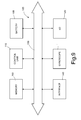
- FIG. 9 illustrates a portion of an electronic system 100 according to one embodiment of the present invention.
- the system 100 incorporates the gyroscope 1 and may be used in devices, such as, for example, a palmtop computer (personal digital assistant, PDA), a laptop or portable computer, possibly with wireless capacity, a cellphone, a messaging device, a digital music reader, a digital camera, or other devices designed to process, store, transmit or receive information.
- the gyroscope 1 may be used in a digital camera for detecting movements and carrying out an image stabilization.
- the gyroscope 1 is included in a portable computer, a PDA, or a cellphone for detecting a free-fall condition and activating a safety configuration.
- the gyroscope 1 is included in a user interface activated by movement for computers or consoles for videogames. In a further embodiment, the gyroscope 1 is incorporated in a satellite-navigation device and is used for temporary tracking of position in the case of loss of the satellite-positioning signal.
- the electronic system 100 may comprise a controller 110, an input/output (I/O) device 120 (for example, a keyboard or a screen), the gyroscope 1, a wireless interface 140, and a memory 160, of a volatile or nonvolatile type, coupled to one another through a bus 150.
- I/O input/output
- a battery 180 may be used for supplying the system 100. It is to be noted that the scope of the present invention is not limited to embodiments having necessarily one or all of the devices listed.
- the controller 110 may comprise, for example, one or more microprocessors, microcontrollers, and the like.
- the I/O device 120 may be used for generating a message.
- the system 100 may use the wireless interface 140 for transmitting and receiving messages to and from a wireless-communications network with a radiofrequency (RF) signal.
- wireless interface may comprise an antenna, a wireless transceiver, such as a dipole antenna, even though the scope of the present invention is not limited from this standpoint.
- the I/O device 120 may supply a voltage representing what is stored either in the form digital output (if digital information has been stored) or in the form analog output (if analog information has been stored).
- the gyroscope could have any different micromechanical structure.
- the invention can be advantageously exploited in: gyroscopes with one or more sensing masses linearly movable with respect to the driving mass and sensitive to rotations of pitch and/or roll (in addition to rotations of yaw); gyroscopes with cantilever sensing masses or sensing masses in the form of beams oscillating about centroidal or non-centroidal axes; and uniaxial and multiaxial gyroscopes with angularly oscillating driving mass.
Landscapes
- Engineering & Computer Science (AREA)
- Physics & Mathematics (AREA)
- General Physics & Mathematics (AREA)
- Radar, Positioning & Navigation (AREA)
- Remote Sensing (AREA)
- Signal Processing (AREA)
- Gyroscopes (AREA)
Abstract
Description
- The present invention relates to a microelectromechanical gyroscope with calibrated synchronization of actuation and to a method for actuating a microelectromechanical gyroscope.
- As is known, the use of microelectromechanical systems (MEMS) has become progressively widespread in various sectors of technology and has yielded encouraging results especially for providing inertial sensors, microintegrated gyroscopes, and electromechanical oscillators for a wide range of applications.
- MEMS of this type are usually based on microelectromechanical structures comprising at least one movable mass connected to a fixed body (stator) by springs and movable with respect to the stator according to pre-determined degrees of freedom. The movable mass is moreover coupled to the fixed body via capacitive structures (capacitors). The movement of the movable mass with respect to the fixed body, for example on account of an external stress, modifies the capacitance of the capacitors; from this it is possible to trace back to the relative displacement of the movable mass with respect to the fixed body and hence to the force applied. Vice versa, by supplying appropriate biasing voltages, it is possible to apply an electrostatic force to the movable mass to set it in motion. In addition, to provide electromechanical oscillators, the frequency response of inertial MEMS structures is exploited, which is typically of the second-order low-pass type.
- Many MEMS (in particular, all electromechanical oscillators and gyroscopes) must include driving devices that have the task of maintaining the movable mass in oscillation.
- A first type of known solution envisages supplying, in open loop, periodic excitation at the resonance frequency of the MEMS structure. The solution is simple, but also far from effective, because the resonance frequency is not known with precision on account of the ineliminable dispersions in the processes of micromachining of semiconductors. In addition, the resonance frequency of each individual device can vary over time, for example, on account of temperature gradients or, more simply, on account of ageing.
- Feedback driving circuits have then been proposed, based upon the use of sigma-delta modulators. Circuits of this type are undoubtedly more effective than the previous ones in stabilizing the oscillation of the movable mass at the real resonance frequency and in suppressing disturbance. However, various stages are necessary for filtering, decimation, and further processing of the bitstream supplied by the sigma-delta modulator. For this reason, currently available feedback driving circuits are complex to produce, cumbersome and, in practice, costly.
- In addition, it should be considered that gyroscopes have a complex electromechanical structure, which comprises two masses that are movable with respect to the stator and are coupled to one another so as to present a relative degree of freedom. The two movable masses are both capacitively coupled to the stator. One of the movable masses is dedicated to driving (driving mass) and is kept in oscillation at the resonance frequency. The other movable mass (sensing mass) is driven in the oscillatory motion and, in the case of rotation of the microstructure with respect to a pre-determined axis with an angular velocity, is subject to a Coriolis force proportional to the angular velocity itself. In practice, the sensing mass operates as an accelerometer that enables sensing of the Coriolis acceleration.
- For enabling actuation and providing an electromechanical oscillator in which the sensor performs the role of frequency-selective amplifier, with transfer function of a second-order low-pass type and high merit factor, the driving mass is equipped with two types of differential capacitive structures: driving electrodes and driving-detection electrodes. The driving electrodes have the purpose of sustaining self-oscillation of the movable mass in the direction of actuation, through electrostatic forces generated by the spectral component of the noise at the mechanical resonance frequency of the driving mass. The driving-detection electrodes have the purpose of measuring, through the transduced charge, the position of translation or rotation of the sensing mass in the direction of actuation.
- The patent No.
EP 1 624 285 - The document No.
EP 1 959 234 describes an improvement of the foregoing control system, in which the control loop comprises a low-pass filter in order to reduce the offset and the effects of parasitic components and couplings by operating on the overall gain and phase of the feedback loop. - These systems, albeit operating frequently in a satisfactory way, may, however, undergo improvement as regards area occupation. In order to preserve the advantages deriving from the use of microstructures with driving and sensing masses not electrically insulated from one another (in particular on account of the technological difficulties in providing the insulation, which render the manufacturing processes considerably more complex and costly), it is in fact necessary to synchronize the read and control circuits precisely. For this purpose, phase-locked-loop (PLL) circuits are normally used, which have, however, a far from negligible impact in terms of area occupation, as well as of consumption levels, and require external filtering components for operating properly. In addition, at the start and upon waking-up from low-consumption (the so-called "power-down") configurations or from conditions of loss of synchronism, the PLL circuits may require transients even of several hundreds of milliseconds before completing phase locking. The consequent delay in the response can be critical in certain applications.
- The aim of the present invention is to provide a microelectromechanical gyroscope and a method for actuating a microelectromechanical gyroscope that will make it possible to overcome the limitations described.
- According to the present invention, a microelectromechanical gyroscope and a method for actuating a microelectromechanical gyroscope are provided, as claimed in
Claim 1 andClaim 15, respectively. - For a better understanding of the invention, some embodiments thereof will now be described, purely by way of nonlimiting example and with reference to the attached drawings, wherein:
-
Figure 1 is a simplified block diagram of a microelectromechanical gyroscope according to one embodiment of the present invention; -
Figure 2 is a top plan view of an enlarged detail of the gyroscope ofFigure 1 ; -
Figure 3 is a top plan view of a further enlarged detail of the gyroscope ofFigure 1 ; -
Figure 4 is a graph regarding signals used in the gyroscope ofFigure 1 ; -
Figure 5 is a more detailed block diagram of a first component of the gyroscope ofFigure 1 ; -
Figure 6 is a more detailed block diagram of a second component of the gyroscope ofFigure 1 ; -
Figure 7 is a more detailed block diagram of a part of the second component ofFigure 6 ; -
Figure 8 is a graph regarding signals used in the gyroscope ofFigure 1 ; and -
Figure 9 is a simplified block diagram of an electronic system incorporating a microelectromechanical gyroscope according to one embodiment of the present invention. -
Figure 1 shows as a whole amicroelectromechanical gyroscope 1, which comprises amicrostructure 2, made of semiconductor material, adriving device 3, aread generator 4, and aread device 5. - The
microstructure 2 is made of semiconductor material and comprises afixed structure 6, adriving mass 7, and at least one sensingmass 8. For simplicity, in the embodiment illustrated herein reference will be made to the case of a uniaxial gyroscope, in which asingle sensing mass 8 is present. What is described hereinafter applies, however, also to the case of multiaxial gyroscopes, which comprise two or more sensing masses or systems of sensing masses, for detecting rotations according to respective independent axes. - The
driving mass 7 is elastically constrained to thefixed structure 6 so as to be able to oscillate about a resting position according to a translational or rotational degree of freedom. Thesensing mass 8 is mechanically coupled to thedriving mass 7 so as to be driven in motion according to the degree of freedom of thedriving mass 7 itself. In addition, thesensing mass 8 is elastically constrained to thedriving mass 7 so as to oscillate in turn with respect to thedriving mass 7 itself, with a respective further degree of freedom. - In the embodiment described herein, in particular, the
driving mass 7 is linearly movable along a driving axis X, while thesensing mass 8 is movable with respect to thedriving mass 7 according to a sensing axis Y, that is perpendicular to the driving axis X. - It is understood, however, that the type of movement (whether translational or rotational) allowed by the degrees of freedom and the arrangement of the driving and sensing axes may vary according to the type of gyroscope. With reference to the movements of the
driving mass 7 and of thesensing mass 8, moreover, the expression "according to an axis" will be indifferently used in relation to movements along an axis or about an axis, according to whether movements allowed to the masses by the respective degrees of freedom are translational (along an axis) or else rotational (about an axis). Likewise, the expression "according to a degree of freedom" will be indifferently used in relation to translational or rotational movements, as allowed by the degree of freedom itself. - In addition, the driving mass 7 (with the sensing mass 8) is connected to the
fixed structure 6 so as to define a resonant mechanical system with a resonance frequency ωR (according to the driving axis X) . - The driving mass 7 (
Figure 2 ) is capacitively coupled to thefixed structure 6 throughdriving units 10 and feedback-sensing units 12. The capacitive coupling is of a differential type. - In greater detail, the
actuation units 10 comprise first and second fixeddriving electrodes fixed structure 6 and extend substantially perpendicular to the driving direction X, andmovable driving electrodes 10c, which are anchored to thedriving mass 7 and are also substantially perpendicular to the driving direction X. Themovable driving electrodes 10c are comb-fingered and capacitively coupled with respective first fixeddriving electrodes 10a and second fixeddriving electrodes 10b. In addition, the first and second fixeddriving electrodes actuation units 10 are electrically connected to afirst driving terminal 13a and to asecond driving terminal 13b, respectively, of themicrostructure 2. Furthermore, as has been mentioned, the coupling is of a differential type. In other words, in eachactuation unit 10 a movement of thedriving mass 7 along the driving axis X causes the capacitance between themovable driving electrode 10c and one of the fixeddriving electrodes movable driving electrode 10c and the other of the fixeddriving electrodes - The structure of the feedback-
sensing units 12 is similar to that of theactuation units 10. In particular, the feedback-sensingunits 12 comprise first and secondfixed sensing electrodes structure 6, andmovable sensing electrodes 12c, anchored to the drivingmass 7 and comb-fingered and capacitively coupled with respective firstfixed sensing electrodes 12a and secondfixed sensing electrodes 12b. In addition, the first and secondfixed sensing electrodes units 12 are electrically connected respectively to a first feedback-sensing terminal 14a and a second feedback-sensing terminal 14b of themicrostructure 2. - Hence, in practice, the driving
mass 7 is coupled to thedriving terminals sensing terminals - The
sensing mass 8 is electrically connected to the drivingmass 7, without interposition of insulating structures. Consequently, thesensing mass 8 and the drivingmass 7 are at the same potential. Thesensing mass 8 is moreover capacitively coupled to the fixedstructure 6 through signal-sensing units 15 (Figure 3 ). More precisely, the signal-sensingunits 15 comprise third and fourthfixed sensing electrodes structure 6, andmovable sensing electrodes 15c, anchored to thesensing mass 8 and arranged between respective thirdfixed sensing electrodes 15a and fourthfixed sensing electrodes 15b. Also in this case, the capacitive coupling is of a differential type, but it is obtained through parallel-plate electrodes, which are perpendicular to the sensing direction Y. In addition, the third and fourthfixed sensing electrodes units 15 are electrically connected, respectively, to a first signal-sensing terminal 17a and to a second signal-sensing terminal 17b of themicrostructure 2. In practice, thesensing mass 8 is coupled to the signal-sensing terminals Figure 1 , the drivingdevice 3 is connected to thedriving terminals sensing terminals microstructure 2 so as to form, with the drivingmass 7, an oscillatingmicroelectromechanical loop 18, with control of position of the drivingmass 7. In greater detail, the drivingdevice 3 comprises acharge amplifier 20, a band-pass filter 21, a low-pass interpolator filter 22, a variable-gain amplifier 23, acontroller 24, acomparator 25, and a digital phase-shifter module 26. In addition, anoscillator 27, a temperature-compensation module 28, asynchronization stage 29, and atiming generator 30 are used for supplying timing signals for thedriving device 3, for theread generator 4, and for theread device 5. - The
microelectromechanical loop 18 is of a hybrid type. Thecharge amplifier 20 is, in fact, of the switched-capacitor type and is configured for operating in discrete time, whereas the low-pass filter 22 and the variable-gain amplifier 23 operate in continuous time. The band-pass filter 21 carries out time-discrete-to-time-continuous conversion. In addition, thecharge amplifier 20 defines a detection interface for detecting the position x of the drivingmass 7 with respect to the driving axis X. The remaining components of thedriving device 3 co-operate for controlling, on the basis of the position x of the drivingmass 7, the amplitude of oscillation of themicroelectromechanical loop 18, in particular the amplitude of oscillation of the drivingmass 7, and maintain it close to a reference amplitude. The reference amplitude is, in particular, determined by a reference voltage VREF, which is supplied to thecontroller 24. - The
charge amplifier 20, which is of a fully differential type and has inputs respectively connected to the first and second feedback-sensing terminals mass 7 with respect to the driving axis X. Thecharge amplifier 20 receives differential feedback charge packets QFB1, QFB2 from the feedback-sensing terminals microstructure 2 and converts them into feedback voltages VFB1, VFB2, indicative of the position x of the drivingmass 7. In this way, thecharge amplifier 20 carries out a discrete-time reading of the position x of the drivingmass 7. - The band-
pass filter 21 is cascaded to thecharge amplifier 20 and introduces a phase shift that is as close as possible to 90° and in any case comprised in the interval 90°+40°. In one embodiment, the band-pass filter 21 comprises a sample-and-hold circuit and is moreover configured so as to carry out a first low-pass filtering. Phase-shifted feedback voltages VFB1', VFB2' supplied by the band-pass filter 21 are thus delayed and attenuated with respect to the feedback voltages VFB1, VFB2. The phase-shifted feedback voltages VFB1', VFB2' present basically step-like variations. - The low-
pass filter 22 is arranged downstream of the band-pass filter 21, is a fully differential filter at least of the second order, and supplies filtered feedback voltages VFB1", VFB2" which are continuously variable in time. The cut-off frequency of the low-pass filter 22 is selected in such a way that the frequency of oscillation of the microelectromechanical loop 18 (in particular of the driving mass 7), hereinafter referred to as driving frequency ωD, is included in the passband and in such a way that the phase of the useful signal indicating the position x of the drivingmass 7 is not substantially altered. In addition, the passband of the low-pass filter 22 is such that the undesirable signal components, linked to sampling by discrete-time reading, are attenuated by at least 20 dB. - In order to prevent offsets that could jeopardize control of the oscillations of the
microelectromechanical loop 18, both the band-pass filter 21 and the low-pass filter 22 are based upon amplifiers provided with auto-zero function. - The variable-
gain amplifier 23 is of a continuous-time fully differential type, is cascaded to the low-pass filter 22, and has outputs connected to thedriving terminals microstructure 2, for supplying driving voltages VD1, VD2 such as to sustain the oscillation of themicroelectromechanical loop 18 at the driving frequency ωD, close to the mechanical resonance frequency ωD of themicrostructure 2. For this purpose, the gain G of the variable-gain amplifier 23 is determined by thecontroller 24 through a control signal VC correlated to the filtered feedback voltages VFB1", VFB2" supplied by the low-pass filter 22. Thecontroller 24 is, for example, a discrete-time PID controller. - In particular, the gain G is determined so as to maintain the conditions of oscillation of the microelectromechanical loop 18 (unit loop gain with phase shift that is an integer multiple of 360°). For this purpose, the
controller 24 receives at input the reference voltage VREF, which indicates the desired reference amplitude of oscillation. - The
comparator 25 has inputs connected to the inputs of the variable-gain amplifier 23, which define control nodes 25a, and receives the difference voltage ΔV between the filtered feedback voltages VFB1", VFB2" at output from the low-pass filter 22. Thecomparator 25 switches at each zero crossing of the difference voltage ΔV, thus operating as frequency-detector device. In one embodiment, thecomparator 25 is connected to a single control node and switches at each zero crossing of one between the filtered feedback voltages VFB1", VFB2" (the zero crossings of the filtered feedback voltages VFB1", VFB2" and of the difference voltage ΔV coincide). - The output of the
comparator 25, which is connected to an input of the phase-shifter module 26, supplies a native clock signal CKN having the current frequency of oscillation of themicroelectromechanical loop 18. The native clock signal CKN is, however, phase-shifted with respect to the driving mass, on account of the presence of thecharge amplifier 20, of the band-pass filter 21, and of the low-pass filter 22. - The phase-
shifter module 26 supplies a quadrature clock signal CK90, which is phase-shifted by 90° with respect to the native clock signal CKN and is used for timing thecontroller 24. In practice, the quadrature clock signal CK90 switches at the maxima and at the minima of the filtered feedback voltages VFB1", VFB2" at output from the low-pass filter 22. Thecontroller 24 is thus properly timed so as to detect the peak values of the difference ΔV between the filtered feedback voltages VFB1", VFB2". - As has been mentioned, the
oscillator 27, the temperature-compensation module 28, thesynchronization stage 29, and thetiming generator 30 co-operate for supplying timing signals for thedriving device 3, for theread generator 4, and for theread device 5. - In greater detail, the
oscillator 27 generates a master clock signal CKM and an auxiliary clock signal CKAUX, in a way asynchronous with respect to the oscillations of themicroelectromechanical loop 18 and, in particular, of the drivingmass 7. Theoscillator 27 is calibrated in the factory so that a master frequency ωM of the master clock signal CKM is equal to an integer multiple N, preferably a power of 2, of the driving frequency ωD of the microelectromechanical loop 18 (ωM = NωD, with N greater than 29, for example equal to 210). For this purpose, a frequency-calibration register 31 is associated to theoscillator 27 and enables modification from outside of the frequency of the master clock signal CKM. The auxiliary clock signal CKAUX, generated by frequency division from the master clock signal CKM, has an auxiliary frequency WAUX equal to ωM/N, i.e., substantially equal to the driving frequency ωD. - The temperature-
compensation module 28 comprises atemperature sensor 28a and amemory 28b. Thetemperature sensor 28a is integrated in the same semiconductor chip as theoscillator 27 and is thermally coupled thereto. Thememory 28b, the contents of which are defined during calibration in the factory, comprises an empirical table of correction values of the frequency as a function of the temperature. In use, thememory 28b returns a correction value Δ (in response to a temperature value T supplied by thetemperature sensor 28a. The correction value extracted is sent to theoscillator 27 and used for compensating the frequency drifts caused by temperature variations, regarding both the mechanical part (microstructure 2) and the electronics (oscillator 27). - The
synchronization stage 29 receives the native clock signal CKN from thecomparator 25 and the auxiliary clock signal CKAUX from theoscillator 27 and is configured to generate a base clock signal CKB according to a first operating mode at steady-state and to a second operating mode in stabilization transients. The stabilization transients occur at start-up (turning-on or exit from a low-consumption, or power-down, configuration), or else when the oscillations of the drivingmass 7 are disturbed as a result of external shocks. - As explained in detail hereinafter, in steady-state conditions the base clock signal CKB is equal to the native clock signal CKN, translated in phase by an amount such as to compensate the phase shift (in advance or in delay) introduced by the components of the
electromechanical loop 18 arranged between the drivingmass 7 and the variable-gain amplifier 23 (i.e., thecharge amplifier 20, the band-pass filter 21, and the low-pass filter 22, in the embodiment described). Hence, in steady-state conditions, the base clock signal CKB has the driving frequency ωD and is in phase with the oscillations of the drivingmass 7. - In the stabilization transients, instead, the base clock signal CKB has the same frequency as the auxiliary clock signal CKAUX- In one embodiment, the base clock signal CKB is also phase-shifted by the amount used for the compensation in steady-state conditions. In effect, in the stabilization transients, the phase is substantially of no effect, and the phase re-alignment may not be carried out. In this case, the base clock signal CKB is synchronous in frequency and phase with the auxiliary clock signal CKAUX.
- The
synchronization stage 29 switches from the second operating mode (transient operation) to the first operating mode (steady-state operation) when the frequency of the native clock signal CKN (i.e., the current frequency of oscillation of the microelectromechanical loop 18) is close to the driving frequency ωD. In order to verify the switching condition, thesynchronization stage 29 compares the frequency of the native clock signal CKN with the frequency of the auxiliary clock signal CKAUX, which is calibrated at the driving frequency ωD. When the difference is lower than a threshold, thesynchronization stage 29 passes from the second operating mode to the first operating mode. Instead, if the difference increases above the threshold, thesynchronization stage 29 returns to the second operating mode. Thetiming generator 30 receives the master clock signal CKM from theoscillator 27 and the base clock signal CKB from thesynchronization stage 29 and uses them for generating the timing signals necessary for the discrete-time components and, more in general, for proper operation of thegyroscope 1. - In particular, the
timing generator 30 supplies a first timing signal Φ1, a second timing signal Φ2, and a third timing signal Φ3, which have sensing frequency equal to an integer multiple of the frequency of the base clock signal CKB (which, in steady-state conditions, coincides with the driving frequency ωD; for example, in one embodiment, the integer multiple is 40). - The
read generator 4 is timed by the third timing signal Φ3 and supplies to the drivingmass 7 and to the sensing mass 8 a square-wave read signal VR with rising and falling edges, respectively, at the start and at the end of the sensing step of each cycle (in practice coinciding with the edges of the third timing signal Φ3). In one embodiment, the read signal VR is a voltage that varies between 0 V and 2VCM, where VCM is a common-mode voltage for the components of themicroelectromechanical loop 18. - The temporal correlation between the read signal VR and the timing signals Φ1, Φ2, Φ3 is illustrated in
Figure 4 and is defined to implement sensing and control cycles according to the correlated-double-sampling (CDS) technique. The first and second timing signals Φ1, Φ2 are high in a first fraction (to- t1) of each cycle (approximately one fifth of the period, reset step), whereas the third timing signal Φ3 is low. Then (instant t1), the first timing signal Φ1 switches and the situation remains unvaried for a second fraction (t1-t2) of the period (approximately two fifths, offset-sampling step; by "offset" is meant, here and in what follows, both the static offset and the contributions of flicker noise associated to the various components). At an instant t2, the second timing signal Φ2 switches and remains stable during the third and last fraction (t2-t3) of the period (once again two fifths, sensing step). - The
read device 5 is of the discrete-time open-loop type and, in the embodiment described herein, is configured to execute a so-called "double-ended" reading of the displacements of thesensing mass 8 according to the respective degree of freedom (in particular, for detecting a position y of the sensing mass along the sensing axis Y). In particular, theread device 5 has inputs connected to the signal-sensing terminals microstructure 2 and an output 5a, which supplies an output signal SOUT, representative of the angular velocity (of themicrostructure 2. - As shown in
Figure 5 , in one embodiment theread device 5 comprises acharge amplifier 32, ademodulator 33, which receives the master clock signal CKM and the base clock signal CKB, a sample-and-hold (S&H)stage 34, a low-pass filter 35, and anoutput amplifier 36, which are cascaded to one another. Thecharge amplifier 32 and thedemodulator 33 are of the switched-capacitor fully differential type. Thegyroscope 1 operates as hereinafter described. In steady-state conditions, the drivingmass 7 is kept in oscillation along the driving axis X by the drivingdevice 3 at the driving frequency ωD and with controlled amplitude. Thesensing mass 8 is driven in motion along the driving axis X by the drivingmass 7. Consequently, when themicrostructure 2 rotates about a gyroscopic axis perpendicular to the plane of the axes X, Y at a certain instantaneous angular velocity Ω, thesensing mass 8 is subject to a Coriolis force, which is parallel to the sensing axis Y and is proportional to the angular velocity (of themicrostructure 2 and to the velocity of the twomasses 
where Ms is the value of thesensing mass 8, (is the angular velocity of themicrostructure 2, and x' is the velocity of the twomasses sensing mass 8 caused by the Coriolis force are read by applying the read signal VR to thesensing mass 8 itself and converting differential charge packets thus produced into the output signal SOUT, by means of theread device 5. - The
controller 24, thecomparator 25, and the phase-shifter module 26 co-operate with the band-pass filter 21, the low-pass filter 22, and the variable-gain amplifier 23 for creating and maintaining the conditions of oscillation of themicroelectromechanical loop 18 in different operating steps of thegyroscope 1. - In particular, in the stabilization transients the oscillations of the driving
mass 7 and, consequently, the signals present in themicroelectromechanical loop 18 do not have a sufficient amplitude to enable proper detection of the zero crossing of the difference voltage ΔV. Thecomparator 25 switches in an incoherent way with respect to the oscillations of the drivingmass 7, because the noise contribution prevails over the useful signal. Consequently, thesynchronization stage 29 operates in the second operating mode, and the base clock signal CKB has the same frequency as the auxiliary clock signal CKAUX (ωD/N). The second operating mode of thesynchronization stage 29 guarantees coordinated timing of the steps of reading of the position of the drivingmass 7 and of thesensing mass 8 even when the oscillations of themicroelectromechanical loop 18 are not sufficiently large to enable thecomparator 25 to detect the frequency correctly. - When the amplitude of the oscillations of the driving
mass 7 approaches the steady-state conditions, the amplitude of the difference voltage ΔV increases and the weight of the noise contribution is reduced accordingly. The recognition of the zero crossing of the difference voltage ΔV tends to become progressively more precise, until thesynchronization stage 29 detects that the frequency of the native clock signal CKN supplied by thecomparator 25 is close to the frequency of the auxiliary clock signal CKAUX and hence to the driving frequency ωD. Thesynchronization stage 29 switches to the first operating mode, and thus the base clock signal CKB is synchronous in frequency and phase with the oscillations of the drivingmass 7. - The synchronism is hence maintained until a power-off command or an energy-save (power-down or sleep-mode) command or else an external event (shock) intervenes.
- The solution described enables proper actuation of the
gyroscope 1, in particular as regards timing of the discrete-time components, and reading of the displacements of the drivingmass 7 and of thesensing mass 8. The synchronization is achieved without the use of phase-locked-loop (PLL) circuits, with considerable saving in terms of area occupation, consumption, and additional components external to the chip. - According to one embodiment, illustrated in
Figure 6 , thesynchronization stage 29 comprises a clock-verifymodule 40, amultiplexer 41, and a phase-alignment module 42, associated to which is a phase-calibration register 43. - The clock-verify
module 40 is connected to thecomparator 25 and to theoscillator 27 for receiving the native clock signal CKN and the auxiliary clock signal CKAUX onrespective comparison inputs module 40 is structured to verify the permanence of the current frequency of the native clock signal CKN in an admissibility range around the driving frequency ωD. The clock-verifymodule 40 supplies a clock lock signal CK_LOCK that has a lock (logic) value, when the current frequency of the native clock signal CKN falls within the admissibility range and an asynchronous-frequency (logic) value in the opposite case. - The
multiplexer 41 hassignal inputs comparator 25 and to theoscillator 27 for receiving the native clock signal CKN and the auxiliary clock signal CKAUX, and a control input 41c, connected to the output of the clock-verifymodule 40 for receiving the clock lock signal CK_LOCK. Themultiplexer 41 moreover has an output connected to the phase-alignment module 42 and transfers at output the native clock signal CKN when the clock lock signal CK_LOCK has the lock value, and the auxiliary clock signal CKAUX when the clock lock signal CK_LOCK has the asynchronous-frequency value. - The phase-
alignment module 42, which receives also the master clock signal CKM from theoscillator 27, applies a calibrated phase shift Δ (to the clock signal received from themultiplexer 41 The calibrated phase shift is stored in the phase-calibration register 43 during calibration in the factory and is substantially equal, in absolute value, to the phase shift introduced by the components of the microelectromechanical loop arranged between the drivingmass 7 and the variable-gain amplifier 23 (i.e., thecharge amplifier 20, the band-pass filter 21, and the low-pass filter 22, in the embodiment described). - Said phase shift is hence eliminated, and the base clock signal CKB is in phase with the oscillations of the driving
mass 7 according to the driving axis X. - The output of the phase-
alignment module 42 is connected to thetiming generator 30 for supplying the base clock signal CKB. -
Figure 7 shows in greater detail the clock-verifymodule 40, which comprises afirst clock counter 45, asecond clock counter 46, an enablingelement 47 and acount comparator 48. - The
first clock counter 45 has a count input (defined by thesecond input 40b) coupled to theoscillator 27 for receiving the auxiliary clock signal CKAUX and stores a first count value C1. - In addition, the
first clock counter 45 is provided with asynchronization logic network 49, which generates a synchronization signal SSYNC. The synchronization signal SSYNC is supplied to the enablingelement 47 and to thecount comparator 48 and has an enabling value when the first count value C1 stored in thefirst clock counter 45 is lower than a control value C1*. When the control value C1* is reached, the synchronization signal SSYNC switches to a disabling value and, moreover, thefirst clock counter 45 is reset. Thesecond clock counter 46 has a count input (defined by thefirst input 40a) coupled to thecomparator 25, for receiving the native clock signal CKN, and an enabling input connected to the enablingelement 47. The second clock counter 46 stores a second count value C2, which is incremented at each cycle of the native clock signal CKN when thesecond clock counter 46 is enabled. - The enabling
element 47 is, for example, a flip-flop of a DT type and receives the synchronization signal SSYNC on a data input from thefirst clock counter 45 and the native clock signal CKN on a clock input from the comparator 125. In this way, the enablingelement 47 transfers the value of the synchronization signal SSYNC to the enabling input of thesecond clock counter 46, which is thus incremented at each cycle of the native clock signal CKN, as long as the synchronization signal SSYNC remains at the enabling value (i.e., until thefirst clock counter 45 reaches the control value C1*). The native clock signal CKN on the clock input of the enablingelement 47 prevents spurious switchings and errors of thesecond clock counter 46. - The
count comparator 48 is coupled to thefirst clock counter 45, from which it receives also the synchronization signal SSYNC, and to thesecond clock counter 46. - The
count comparator 48 supplies at output the clock lock signal CK_LOCK and determines the value thereof as described hereinafter. - When the first clock counter 45 starts a count after having been reset, the synchronization signal SSYNC switches to the enabling value (as shown in
Figure 8 , which regards a start-up step in which the driving mass is forced into oscillation starting from a resting condition). Thesecond clock counter 46 is enabled and is incremented at each cycle of the native clock signal CKN, independently of thefirst clock counter 45. In addition, the current frequency of the native clock signal CKN progressively approaches the frequency of the auxiliary clock signal CKAUX, as a result of the increase in amplitude of the oscillations due to forcing. The frequency variations of the native clock sig - nal CKN are illustrated in an exaggerated way inFigure 8 . When thefirst clock counter 45 reaches the control value C1*, the synchronization signal SSYNC switches to the disabling value, and the final count value C2* stored in thesecond clock counter 46 is frozen. - In addition, the
count comparator 48 takes the control value C1* and the final count value C2*, respectively, from thefirst clock counter 45 and from thesecond clock counter 46 and assigns a value to the clock lock signal CK_LOCK according to whether the lock condition:
is verified or not. - More precisely, if the control value C1* and the final count value C2* satisfy the lock condition, assigned to the clock lock signal CK_LOCK is the lock value. In this case, in fact, the current frequency of the native clock signal CKN is close to the frequency of the auxiliary clock signal CKAUX and hence to the driving frequency ωD.
- In the opposite case, i.e., if the inequality is not verified, the
count comparator 48 assigns to the clock lock signal CK_LOCK the asynchronous-frequency value. -
Figure 9 illustrates a portion of anelectronic system 100 according to one embodiment of the present invention. Thesystem 100 incorporates thegyroscope 1 and may be used in devices, such as, for example, a palmtop computer (personal digital assistant, PDA), a laptop or portable computer, possibly with wireless capacity, a cellphone, a messaging device, a digital music reader, a digital camera, or other devices designed to process, store, transmit or receive information. For example, thegyroscope 1 may be used in a digital camera for detecting movements and carrying out an image stabilization. In other embodiments, thegyroscope 1 is included in a portable computer, a PDA, or a cellphone for detecting a free-fall condition and activating a safety configuration. In a further embodiment, thegyroscope 1 is included in a user interface activated by movement for computers or consoles for videogames. In a further embodiment, thegyroscope 1 is incorporated in a satellite-navigation device and is used for temporary tracking of position in the case of loss of the satellite-positioning signal. - The
electronic system 100 may comprise acontroller 110, an input/output (I/O) device 120 (for example, a keyboard or a screen), thegyroscope 1, awireless interface 140, and amemory 160, of a volatile or nonvolatile type, coupled to one another through abus 150. In one embodiment, abattery 180 may be used for supplying thesystem 100. It is to be noted that the scope of the present invention is not limited to embodiments having necessarily one or all of the devices listed. - The
controller 110 may comprise, for example, one or more microprocessors, microcontrollers, and the like. - The I/
O device 120 may be used for generating a message. Thesystem 100 may use thewireless interface 140 for transmitting and receiving messages to and from a wireless-communications network with a radiofrequency (RF) signal. Examples of wireless interface may comprise an antenna, a wireless transceiver, such as a dipole antenna, even though the scope of the present invention is not limited from this standpoint. In addition, the I/O device 120 may supply a voltage representing what is stored either in the form digital output (if digital information has been stored) or in the form analog output (if analog information has been stored). - Finally, it is clear that modifications and variations may be made to the gyroscope and to the method described, without thereby departing from the scope of the present invention, as defined in the annexed claims.
- In particular, the gyroscope could have any different micromechanical structure. For example, the invention can be advantageously exploited in: gyroscopes with one or more sensing masses linearly movable with respect to the driving mass and sensitive to rotations of pitch and/or roll (in addition to rotations of yaw); gyroscopes with cantilever sensing masses or sensing masses in the form of beams oscillating about centroidal or non-centroidal axes; and uniaxial and multiaxial gyroscopes with angularly oscillating driving mass.
Claims (15)
- Microelectromechanical gyroscope comprising:a body (6);a driving mass (7), movable with respect to the body (6) with a first degree of freedom according to a driving axis (X), and a sensing mass (8), mechanically coupled to the driving mass (7) so as to be drawn in motion according to the driving axis (X) and movable with respect to the driving mass (7) with a second degree of freedom according to a sensing axis (Y), in response to rotations of the body (6);a driving device (3), forming a microelectromechanical control loop (18) with the body (6) and the driving mass (7) and configured to maintain the driving mass (7) in oscillation according to the driving axis (X) with a driving frequency (ωD);wherein the driving device (3) comprises a frequency detector module (25), connected to a control node (25a) of the microelectromechanical control loop (18) and configured to provide a first clock signal (CKN), with a frequency equal to a current oscillation frequency of the driving mass (7) ;characterized in that the driving device (3) comprises a synchronization stage (29), configured to apply, in a first operation mode, a calibrated phase shift (Δϕ) to the first clock signal (CKN), so as to compensate a phase shift caused by components (20, 21, 22) of the microelectromechanical control loop (18) arranged between the driving mass (7) and the control node (25a).
- Gyroscope according to claim 1, wherein the synchronization stage (29) is configured to provide a second clock signal (CKB) that, in the first operation mode, has the same frequency as the first clock signal (CKN) and a phase shift equal to the calibrated phase shift (Δϕ).
- Gyroscope according to claim 2, comprising a timing generator (30), configured to provide a plurality of timing signals (Φ1, Φ2, Φ3) on the basis of the second clock signal (CKB) .
- Gyroscope according to claim 3, wherein the timing signals (Φ1, Φ2, Φ3) have frequency equal to an integer multiple of the frequency of the second clock signal (CKB).
- Gyroscope according to claim 3 or 4, wherein the microelectromechanical control loop (18) comprises at least a switched-capacitor component (20), operated through the timing signals (Φ1, Φ2, Φ3).
- Gyroscope according to any one of claims 3 to 5, comprising a reading generator (VR), coupled to the driving mass (7) and to the sensing mass (8) for providing a square-wave reading signal (VR) .
- Gyroscope according to any one of claims 3 to 6, wherein the reading generator (VR) is timed through at least one of the timing signals (Φ1, Φ2, (Φ3).
- Gyroscope according to any one of claims 2 to 7, comprising an oscillator (27) asynchronous with respect to the microelectromechanical control loop (18) and calibrated so as to provide a third clock signal (CKAUX) having an auxiliary frequency (ωAUX) close to the driving frequency (ωD).
- Gyroscope according to claim 8, wherein, in a second operation mode, the second clock signal (CKB) has the auxiliary frequency (ωAUX) of the third clock signal (CKAUX).
- Gyroscope according to claim 9, wherein the synchronization stage (29) is configured to compare the frequency of the first clock signal (CKN) with the auxiliary frequency (ωAUX) of the third clock signal (CKAUX) and to switch from the second operation mode to the first operation mode, when the difference between the frequency of the first clock signal (CKN) and the auxiliary frequency (ωAUX) of the third clock signal (CKAUX) falls below a threshold, and from the first operation mode to the second operation mode, when the difference between the frequency of the first clock signal (CKN) and the auxiliary frequency (ωAUX) of the third clock signal (CKAUX) exceeds the threshold.
- Gyroscope according to claim 9 o 10, wherein the synchronization stage (29) comprises:a clock verify module (40), coupled to the frequency detector module (25) and to the oscillator (27), for receiving respectively the first clock signal (CKN) and the third clock signal (CKAUX), and configured to provide a clock lock signal (CK_LOCK) having a first logic value, when the frequency of the first clock signal (CKN) is within an acceptability range around the driving frequency (ωD), and a second logic value, when the frequency of the first clock signal (CKN) is out of the acceptability range;a selector (41), coupled to the frequency detector module (25) and to the oscillator (27), for receiving respectively the first clock signal (CKN) and the third clock signal (CKAUX), and controlled by the clock verify module (40) for providing the first clock signal (CKN) on output, when the clock lock signal (CK_LOCK) has the first logic value, and the third clock signal (CKAUX), when the clock lock signal (CK_LOCK) has the second logic value; anda phase alignment module (42), configured to apply the calibrated phase shift (Δϕ) to the first clock signal (CKN) when the clock lock signal (CK_LOCK) has the first logic value.
- Gyroscope according to any one of claims 8 to 11, comprising a temperature compensation module (28), coupled to the oscillator (27) for compensating frequency drifts caused by temperature variations.
- Gyroscope according to claim 12, wherein the temperature compensation module (28) comprises a temperature sensor (28a), thermally coupled to the oscillator (27), and a memory (28b), containing a plurality of correction values (Δω) and configured to return respective correction values (Δω) in response to temperature values (T) provided by the temperature sensor (28a).
- System comprising a control unit (410) and a microelectromechanical gyroscope (1) according to any one of claims 1 to 13 coupled to the control unit (410).
- Method for actuating a microelectromechanical gyroscope, wherein the microelectromechanical gyroscope comprises a body (6), a driving mass (7), movable with respect to the body (6) with a first degree of freedom according to a driving axis (X), and a sensing mass (8), mechanically coupled to the driving mass (7) so as to be drawn in motion according to the driving axis (X) and movable with respect to the driving mass (7) with a second degree of freedom according to a sensing axis (Y), in response to rotations of the body (6);
the method comprising:maintaining the driving mass (7) in oscillation according to the driving axis (X) with a driving frequency (ω D) through a microelectromechanical control loop (18) including the body (6) and the driving mass (7); anddetecting a current oscillation frequency of the driving mass (7) at a control node (25a) of the microelectromechanical control loop (18);characterized by applying, at least in one operation mode, a calibrated phase shift (Δϕ) to the first clock signal (CKN), so as to compensate a phase shift caused by components (20, 21, 22) of the microelectromechanical control loop (18) arranged between the driving mass (7) and the control node.
Applications Claiming Priority (1)
| Application Number | Priority Date | Filing Date | Title |
|---|---|---|---|
| ITTO20100106 | 2010-02-15 |
Publications (2)
| Publication Number | Publication Date |
|---|---|
| EP2360448A1 true EP2360448A1 (en) | 2011-08-24 |
| EP2360448B1 EP2360448B1 (en) | 2015-08-26 |
Family
ID=42668367
Family Applications (1)
| Application Number | Title | Priority Date | Filing Date |
|---|---|---|---|
| EP11154596.8A Active EP2360448B1 (en) | 2010-02-15 | 2011-02-15 | Microelectromechanical gyroscope with calibrated synchronization of actuation and method for actuating a microelectromechanical gyroscope |
Country Status (3)
| Country | Link |
|---|---|
| US (2) | US8539834B2 (en) |
| EP (1) | EP2360448B1 (en) |
| CN (1) | CN102230799B (en) |
Cited By (10)
| Publication number | Priority date | Publication date | Assignee | Title |
|---|---|---|---|---|
| CN102621884A (en) * | 2012-01-12 | 2012-08-01 | 西北工业大学 | Six-order continuous band-pass sigma-delta closed-loop control circuit for MEMS (micro-electromechanical system) gyroscope |
| WO2015075499A1 (en) * | 2013-11-22 | 2015-05-28 | Freescale Semiconductor, Inc. | In-band beating removal for a mems gyroscope |
| CN104685319A (en) * | 2012-03-21 | 2015-06-03 | 路梅戴尼科技公司 | Apparatus and method for providing in-plane inertial device with integrated clock |
| WO2015121780A3 (en) * | 2014-02-12 | 2015-11-26 | Murata Manufacturing Co., Ltd. | A drive circuitry for a MEMS resonator |
| US9705450B2 (en) | 2011-06-24 | 2017-07-11 | The United States Of America As Represented By The Secretary Of The Navy | Apparatus and methods for time domain measurement of oscillation perturbations |
| US9715480B1 (en) | 2011-06-24 | 2017-07-25 | United States Of America As Represented By Secretary Of The Navy | Method for analytical reconstruction of digital signals via stitched polynomial fitting |
| WO2017195020A1 (en) | 2016-05-11 | 2017-11-16 | Murata Manufacturing Co., Ltd. | A secondary sense loop with force feedback capability |
| US9829317B2 (en) | 2014-02-12 | 2017-11-28 | Murata Manufacturing Co., Ltd. | Drive circuit for MEMS resonator startup |
| EP3249357A1 (en) | 2016-05-11 | 2017-11-29 | Murata Manufacturing Co., Ltd. | A digital controller for a mems gyroscope |
| EP3361216A1 (en) * | 2017-02-08 | 2018-08-15 | Murata Manufacturing Co., Ltd. | System and method for resonator amplitude control |
Families Citing this family (41)
| Publication number | Priority date | Publication date | Assignee | Title |
|---|---|---|---|---|
| EP1962054B1 (en) * | 2007-02-13 | 2011-07-20 | STMicroelectronics Srl | Microelectromechanical gyroscope with open loop reading device and control method of a microelectromechanical gyroscope |
| IT1394898B1 (en) * | 2009-06-03 | 2012-07-20 | St Microelectronics Rousset | MICROELETTROMECHANICAL GYROSCOPE WITH POSITION CONTROL AND METHOD FOR THE CONTROL OF A MICROELECTRANOMANICAL GYROSCOPE |
| US8539834B2 (en) * | 2010-02-15 | 2013-09-24 | Stmicroelectronics S.R.L. | Microelectromechanical gyroscope with calibrated synchronization of actuation and method for actuating a microelectromechanical gyroscope |
| EP2792069B1 (en) * | 2011-12-16 | 2016-11-02 | Analog Devices, Inc. | Low noise amplifier for multiple channels |
| US9116562B2 (en) | 2012-07-04 | 2015-08-25 | Freescale Semiconductor, Inc. | Digital sample clock generator, a vibration gyroscope circuitry comprising such digital sample clock generator, an associated apparatus, an associated semiconductor device and associated methods |
| WO2014023993A1 (en) * | 2012-08-08 | 2014-02-13 | Freescale Semiconductor, Inc. | Micro-electro-mechanical system drive-mode oscillator module and method therefor |
| US9146109B2 (en) * | 2012-11-26 | 2015-09-29 | Stmicroelectronics S.R.L. | Microelectromechanical gyroscope with improved start-up phase, system including the microelectromechanical gyroscope, and method for speeding-up the start up phase |
| ITTO20121116A1 (en) * | 2012-12-20 | 2014-06-21 | St Microelectronics Srl | CIRCUIT AND DYNAMIC COMPENSATION METHOD OF OFFSET FOR A MEMS SENSOR DEVICE |
| US9541396B2 (en) * | 2013-01-22 | 2017-01-10 | MCube Inc. | Multi-axis integrated inertial sensing device |
| US10107625B2 (en) | 2013-01-22 | 2018-10-23 | MCube Inc. | Integrated inertial sensing device |
| US9612119B2 (en) * | 2013-01-22 | 2017-04-04 | MCube Inc. | Integrated inertial sensing device |
| CN103148846B (en) * | 2013-02-25 | 2015-03-18 | 哈尔滨工业大学 | Micromechanical gyroscope driving device based on arbitrary waveform of DDS (Direct Digital Frequency Synthesizer) |
| US9103845B2 (en) * | 2013-03-08 | 2015-08-11 | Freescale Semiconductor Inc. | System and method for reducing offset variation in multifunction sensor devices |
| JP6194606B2 (en) * | 2013-03-22 | 2017-09-13 | セイコーエプソン株式会社 | Detection device, sensor, gyro sensor, electronic device, and moving object |
| JP6197323B2 (en) * | 2013-03-22 | 2017-09-20 | セイコーエプソン株式会社 | Detection device, sensor, gyro sensor, electronic device, and moving object |
| US9335340B2 (en) * | 2013-07-23 | 2016-05-10 | Freescale Semiconductor, Inc. | MEMS parameter identification using modulated waveforms |
| US10030976B2 (en) * | 2015-05-13 | 2018-07-24 | Kionix, Inc. | Phase-based measurement and control of a gyroscope |
| CN107636473B (en) | 2015-05-20 | 2020-09-01 | 卢米达因科技公司 | Extract inertial information from nonlinear periodic signals |
| US10252920B2 (en) * | 2015-09-07 | 2019-04-09 | International Business Machines Corporation | Flowfield sensors for monitoring liquid flow |
| US10234477B2 (en) * | 2016-07-27 | 2019-03-19 | Google Llc | Composite vibratory in-plane accelerometer |
| JP6602274B2 (en) * | 2016-08-08 | 2019-11-06 | 日立オートモティブシステムズ株式会社 | Inertial detection device |
| IT201700103058A1 (en) * | 2017-09-14 | 2019-03-14 | St Microelectronics Srl | CIRCUIT AND DRIVING METHOD FOR A MEMS GYROSCOPE AND ITS MEMS GYROSCOPE |
| US11796831B2 (en) | 2018-12-17 | 2023-10-24 | Semiconductor Components Industries, Llc | Methods and system for position stabilization |
| US11175138B2 (en) | 2019-06-26 | 2021-11-16 | Stmicroelectronics, Inc. | MEMS gyroscope control circuit |
| US11255670B2 (en) | 2019-06-26 | 2022-02-22 | Stmicroelectronics, Inc. | MEMS gyroscope self-test using a technique for deflection of the sensing mobile mass |
| US11162790B2 (en) | 2019-06-26 | 2021-11-02 | Stmicroelectronics, Inc. | MEMS gyroscope start-up process and circuit |
| US11320452B2 (en) | 2019-06-26 | 2022-05-03 | Stmicroelectronics, Inc. | MEMS accelerometer self-test using an active mobile mass deflection technique |
| DE102019210305A1 (en) * | 2019-07-11 | 2021-01-14 | Infineon Technologies Ag | Controlling an oscillation system |
| DE102019215737B4 (en) * | 2019-10-14 | 2021-05-12 | Robert Bosch Gmbh | Readout circuit for a MEMS gyroscope and method for operating such a readout circuit |
| DE102019219630A1 (en) * | 2019-12-13 | 2021-06-17 | Robert Bosch Gmbh | Phase locked loop for a driver circuit for operating a MEMS gyroscope |
| DE102019220544A1 (en) * | 2019-12-23 | 2021-06-24 | Robert Bosch Gmbh | Sensor arrangement and method for operating a sensor arrangement |
| CN111998842B (en) * | 2020-06-30 | 2022-07-12 | 浙江大学 | On-line compensation method and system for phase delay of micromechanical gyroscope interface circuit |
| EP3965291B1 (en) * | 2020-09-07 | 2024-08-14 | The Swatch Group Research and Development Ltd | Crystal oscillator and startup method for a crystal oscillator |
| WO2022082018A1 (en) * | 2020-10-17 | 2022-04-21 | The Regents Of The University Of California | Precision gyroscope mode-matching insensitive to rate input |
| IT202100016880A1 (en) * | 2021-06-28 | 2022-12-28 | St Microelectronics Srl | MICROELECTROMECHANICAL GYRO WITH DRIVEN RESONANT RING WITH CONTROLLED AMPLITUDE OF OSCILLATION AND METHOD FOR CONTROLLING A MICROELECTROMECHANICAL GYRO |
| CN114993278A (en) * | 2022-05-30 | 2022-09-02 | 四川微著科技有限公司 | MEMS gyroscope open loop reading circuit |
| CN115307660B (en) * | 2022-10-12 | 2023-02-03 | 天津大学 | Broadband calibration device and calibration method suitable for calibrating angular vibration sensor |
| DE102022211691A1 (en) | 2022-11-07 | 2024-05-08 | Robert Bosch Gesellschaft mit beschränkter Haftung | System and method for determining a frequency and/or frequency change of a drive vibration of an inertial sensor |
| IT202300010326A1 (en) * | 2023-05-22 | 2024-11-22 | St Microelectronics Int Nv | MICROELECTROMECHANICAL ACCELEROMETER WITH FORCE FEEDBACK RING |
| US20250102301A1 (en) * | 2023-09-26 | 2025-03-27 | Analog Devices, Inc. | Apparatus and methods for gyroscope signal demodulation |
| US20250377376A1 (en) * | 2024-06-11 | 2025-12-11 | Honeywell International Inc. | Accelerometer with proof mass displacement reduction feature |
Citations (3)
| Publication number | Priority date | Publication date | Assignee | Title |
|---|---|---|---|---|
| EP1624285A1 (en) | 2004-08-03 | 2006-02-08 | STMicroelectronics S.r.l. | Resonant micro-electro-mechanical system and gyroscope |
| US20080111585A1 (en) * | 2006-11-10 | 2008-05-15 | Seiko Epson Corporation | Detection device, sensor, and electronic instrument |
| EP1959234A1 (en) | 2007-02-13 | 2008-08-20 | STMicroelectronics S.r.l. | Microelectromechanical gyroscope with suppression of capacitive coupling spurious signals and control method of a microelectromechanical gyroscope |
Family Cites Families (18)
| Publication number | Priority date | Publication date | Assignee | Title |
|---|---|---|---|---|
| US6585338B2 (en) | 2000-12-22 | 2003-07-01 | Honeywell International Inc. | Quick start resonant circuit control |
| FR2823619B1 (en) | 2001-04-11 | 2003-06-27 | Commissariat Energie Atomique | SIGMA-DELTA BANDWAY MODULATOR AND USES OF THE SIGMA DELTA MOLOR FOR CONVERSION, DETECTION AND PRODUCTION OF SIGNALS |
| DE60120921T2 (en) | 2001-04-27 | 2007-02-01 | Stmicroelectronics S.R.L., Agrate Brianza | Integrated gyro made of semiconductor material |
| US7679463B2 (en) | 2004-03-22 | 2010-03-16 | Mobius Microsystems, Inc. | Multi-terminal harmonic oscillator integrated circuit with frequency calibration and frequency configuration |
| EP1715580B1 (en) * | 2005-03-31 | 2018-11-28 | STMicroelectronics Srl | Device for controlling the resonance frequency of a MEMS resonator |
| JP2006349409A (en) * | 2005-06-14 | 2006-12-28 | Denso Corp | Sensor circuit of electrostatic drive / capacitance detection type gyro sensor |
| DE102005034702A1 (en) | 2005-07-26 | 2007-02-01 | Robert Bosch Gmbh | Method and circuit arrangement for safe startup of a rotation rate sensor |
| DE102005043559A1 (en) * | 2005-09-12 | 2007-03-15 | Siemens Ag | Method and arrangement for monitoring a sensor arrangement |
| EP1832841B1 (en) | 2006-03-10 | 2015-12-30 | STMicroelectronics Srl | Microelectromechanical integrated sensor structure with rotary driving motion |
| JP4396725B2 (en) * | 2006-05-12 | 2010-01-13 | セイコーエプソン株式会社 | Detection device, gyro sensor, and electronic device |
| EP2023082B1 (en) * | 2007-07-05 | 2010-09-08 | STMicroelectronics Srl | Micro-electro-mechanical gyroscope with open-loop reading device and control method thereof |
| JP4576441B2 (en) * | 2008-03-21 | 2010-11-10 | 日立オートモティブシステムズ株式会社 | Angular velocity sensor |
| CN101271125B (en) * | 2008-05-12 | 2011-05-11 | 清华大学 | Capacitance type micro-accelerometer |
| IT1394898B1 (en) | 2009-06-03 | 2012-07-20 | St Microelectronics Rousset | MICROELETTROMECHANICAL GYROSCOPE WITH POSITION CONTROL AND METHOD FOR THE CONTROL OF A MICROELECTRANOMANICAL GYROSCOPE |
| EP2336717B1 (en) * | 2009-12-21 | 2012-09-19 | STMicroelectronics Srl | Microelectromechanical device having an oscillating mass, and method for controlling a microelectromechanical device having an oscillating mass |
| IT1397594B1 (en) * | 2009-12-21 | 2013-01-16 | St Microelectronics Rousset | MICROELETTROMECHANICAL GYROSCOPE WITH CONTINUOUS SELF-TEST FUNCTION AND METHOD OF CONTROL OF A MICROELECTRANOMIC GYROSCOPE. |
| US8539834B2 (en) * | 2010-02-15 | 2013-09-24 | Stmicroelectronics S.R.L. | Microelectromechanical gyroscope with calibrated synchronization of actuation and method for actuating a microelectromechanical gyroscope |
| US8714012B2 (en) * | 2010-02-16 | 2014-05-06 | Stmicroelectronics S.R.L. | Microelectromechanical gyroscope with inversion of actuation forces, and method for actuating a microelectromechanical gyroscope |
-
2011
- 2011-02-14 US US13/026,941 patent/US8539834B2/en active Active
- 2011-02-15 EP EP11154596.8A patent/EP2360448B1/en active Active
- 2011-02-15 CN CN201110085679.5A patent/CN102230799B/en active Active
-
2013
- 2013-05-03 US US13/886,774 patent/US9234755B2/en active Active
Patent Citations (3)
| Publication number | Priority date | Publication date | Assignee | Title |
|---|---|---|---|---|
| EP1624285A1 (en) | 2004-08-03 | 2006-02-08 | STMicroelectronics S.r.l. | Resonant micro-electro-mechanical system and gyroscope |
| US20080111585A1 (en) * | 2006-11-10 | 2008-05-15 | Seiko Epson Corporation | Detection device, sensor, and electronic instrument |
| EP1959234A1 (en) | 2007-02-13 | 2008-08-20 | STMicroelectronics S.r.l. | Microelectromechanical gyroscope with suppression of capacitive coupling spurious signals and control method of a microelectromechanical gyroscope |
Cited By (20)
| Publication number | Priority date | Publication date | Assignee | Title |
|---|---|---|---|---|
| US9705450B2 (en) | 2011-06-24 | 2017-07-11 | The United States Of America As Represented By The Secretary Of The Navy | Apparatus and methods for time domain measurement of oscillation perturbations |
| US10027281B2 (en) | 2011-06-24 | 2018-07-17 | The United States Of America As Represented By The Secretary Of The Navy | Time domain switched ring/disc resonant gyroscope |
| US9715480B1 (en) | 2011-06-24 | 2017-07-25 | United States Of America As Represented By Secretary Of The Navy | Method for analytical reconstruction of digital signals via stitched polynomial fitting |
| CN102621884B (en) * | 2012-01-12 | 2013-10-09 | 西北工业大学 | Six-order continuous band-pass sigma-delta closed-loop control circuit for MEMS (micro-electromechanical system) gyroscope |
| CN102621884A (en) * | 2012-01-12 | 2012-08-01 | 西北工业大学 | Six-order continuous band-pass sigma-delta closed-loop control circuit for MEMS (micro-electromechanical system) gyroscope |
| CN104685319A (en) * | 2012-03-21 | 2015-06-03 | 路梅戴尼科技公司 | Apparatus and method for providing in-plane inertial device with integrated clock |
| EP2828619A4 (en) * | 2012-03-21 | 2016-04-20 | Us Navy | DEVICE AND METHOD FOR PROVIDING AN INERTIAL DEVICE IN THE PLAN WITH AN INTEGRATED CLOCK |
| US10119822B2 (en) | 2013-11-22 | 2018-11-06 | Nxp Usa, Inc. | In-band beating removal for a MEMS gyroscope |
| CN105899910A (en) * | 2013-11-22 | 2016-08-24 | 飞思卡尔半导体公司 | In-Band Runout Removal for MEMS Gyroscopes |
| WO2015075499A1 (en) * | 2013-11-22 | 2015-05-28 | Freescale Semiconductor, Inc. | In-band beating removal for a mems gyroscope |
| CN105899910B (en) * | 2013-11-22 | 2019-01-18 | 恩智浦美国有限公司 | In-Band Bounce Removal for MEMS Gyroscopes |
| US9644961B2 (en) | 2014-02-12 | 2017-05-09 | Murata Manufacturing Co., Ltd. | Drive circuit for a MEMS resonator |
| US9829317B2 (en) | 2014-02-12 | 2017-11-28 | Murata Manufacturing Co., Ltd. | Drive circuit for MEMS resonator startup |
| WO2015121780A3 (en) * | 2014-02-12 | 2015-11-26 | Murata Manufacturing Co., Ltd. | A drive circuitry for a MEMS resonator |
| WO2017195020A1 (en) | 2016-05-11 | 2017-11-16 | Murata Manufacturing Co., Ltd. | A secondary sense loop with force feedback capability |
| EP3249357A1 (en) | 2016-05-11 | 2017-11-29 | Murata Manufacturing Co., Ltd. | A digital controller for a mems gyroscope |
| US10365104B2 (en) | 2016-05-11 | 2019-07-30 | Murata Manufacturing Co., Ltd. | Digital controller for a MEMS gyroscope |
| US11112248B2 (en) | 2016-05-11 | 2021-09-07 | Murata Manufacturing Co., Ltd. | Secondary sense loop with force feedback capability |
| EP3361216A1 (en) * | 2017-02-08 | 2018-08-15 | Murata Manufacturing Co., Ltd. | System and method for resonator amplitude control |
| US10418962B2 (en) | 2017-02-08 | 2019-09-17 | Murata Manufacturing Co., Ltd. | System and method for resonator amplitude control |
Also Published As
| Publication number | Publication date |
|---|---|
| US8539834B2 (en) | 2013-09-24 |
| CN102230799A (en) | 2011-11-02 |
| EP2360448B1 (en) | 2015-08-26 |
| US9234755B2 (en) | 2016-01-12 |
| US20130239680A1 (en) | 2013-09-19 |
| CN102230799B (en) | 2015-11-25 |
| US20110197674A1 (en) | 2011-08-18 |
Similar Documents
| Publication | Publication Date | Title |
|---|---|---|
| EP2360448B1 (en) | Microelectromechanical gyroscope with calibrated synchronization of actuation and method for actuating a microelectromechanical gyroscope | |
| EP2360449B1 (en) | Microelectromechanical gyroscope with inversion of actuation forces, and method for actuating a microelectromechanical gyroscope | |
| EP2259019B1 (en) | Microelectromechanical gyroscope with position control driving and method for controlling a microelectromechanical gyroscope | |
| US10480944B2 (en) | Microelectromechanical gyroscope with compensation of quadrature signal components | |
| US9146109B2 (en) | Microelectromechanical gyroscope with improved start-up phase, system including the microelectromechanical gyroscope, and method for speeding-up the start up phase | |
| EP1962054B1 (en) | Microelectromechanical gyroscope with open loop reading device and control method of a microelectromechanical gyroscope | |
| US7980135B2 (en) | Microelectromechanical gyroscope with self-test function and control method | |
| US8667842B2 (en) | Variable capacitance electronic device and microelectromechanical device incorporating such electronic device | |
| US7827864B2 (en) | Microelectromechanical gyroscope with suppression of capacitive coupling spurious signals and control method | |
| US20130025368A1 (en) | Microelectromechanical gyroscope with improved reading stage and method | |
| US9829319B2 (en) | Microelectromechanical device having an oscillating mass and a forcing stage, and method of controlling a microelectromechanical device | |
| EP4113061B1 (en) | Microelectromechanical gyroscope having a resonant driving loop with controlled oscillation amplitude and method of controlling a microelectromechanical gyroscope |
Legal Events
| Date | Code | Title | Description |
|---|---|---|---|
| PUAI | Public reference made under article 153(3) epc to a published international application that has entered the european phase |
Free format text: ORIGINAL CODE: 0009012 |
|
| PUAI | Public reference made under article 153(3) epc to a published international application that has entered the european phase |
Free format text: ORIGINAL CODE: 0009012 |
|
| AK | Designated contracting states |
Kind code of ref document: A1 Designated state(s): AL AT BE BG CH CY CZ DE DK EE ES FI FR GB GR HR HU IE IS IT LI LT LU LV MC MK MT NL NO PL PT RO RS SE SI SK SM TR |
|
| AX | Request for extension of the european patent |
Extension state: BA ME |
|
| 17P | Request for examination filed |
Effective date: 20120224 |
|
| RAP1 | Party data changed (applicant data changed or rights of an application transferred) |
Owner name: STMICROELECTRONICS SRL |
|
| 17Q | First examination report despatched |
Effective date: 20131220 |
|
| RIC1 | Information provided on ipc code assigned before grant |
Ipc: G01C 19/56 20120101AFI20150128BHEP Ipc: G01C 19/5762 20120101ALI20150128BHEP |
|
| GRAP | Despatch of communication of intention to grant a patent |
Free format text: ORIGINAL CODE: EPIDOSNIGR1 |
|
| RIC1 | Information provided on ipc code assigned before grant |
Ipc: G01C 19/5726 20120101ALI20150224BHEP Ipc: G01C 19/56 20120101AFI20150224BHEP Ipc: G01C 19/5762 20120101ALI20150224BHEP |
|
| INTG | Intention to grant announced |
Effective date: 20150316 |
|
| GRAS | Grant fee paid |
Free format text: ORIGINAL CODE: EPIDOSNIGR3 |
|
| GRAA | (expected) grant |
Free format text: ORIGINAL CODE: 0009210 |
|
| AK | Designated contracting states |
Kind code of ref document: B1 Designated state(s): AL AT BE BG CH CY CZ DE DK EE ES FI FR GB GR HR HU IE IS IT LI LT LU LV MC MK MT NL NO PL PT RO RS SE SI SK SM TR |
|
| REG | Reference to a national code |
Ref country code: GB Ref legal event code: FG4D |
|
| REG | Reference to a national code |
Ref country code: CH Ref legal event code: EP |
|
| REG | Reference to a national code |
Ref country code: AT Ref legal event code: REF Ref document number: 745450 Country of ref document: AT Kind code of ref document: T Effective date: 20150915 |
|
| REG | Reference to a national code |
Ref country code: IE Ref legal event code: FG4D |
|
| REG | Reference to a national code |
Ref country code: DE Ref legal event code: R096 Ref document number: 602011019068 Country of ref document: DE |
|
| REG | Reference to a national code |
Ref country code: AT Ref legal event code: MK05 Ref document number: 745450 Country of ref document: AT Kind code of ref document: T Effective date: 20150826 |
|
| REG | Reference to a national code |
Ref country code: FR Ref legal event code: PLFP Year of fee payment: 6 |
|
| REG | Reference to a national code |
Ref country code: LT Ref legal event code: MG4D |
|
| PG25 | Lapsed in a contracting state [announced via postgrant information from national office to epo] |
Ref country code: FI Free format text: LAPSE BECAUSE OF FAILURE TO SUBMIT A TRANSLATION OF THE DESCRIPTION OR TO PAY THE FEE WITHIN THE PRESCRIBED TIME-LIMIT Effective date: 20150826 Ref country code: LT Free format text: LAPSE BECAUSE OF FAILURE TO SUBMIT A TRANSLATION OF THE DESCRIPTION OR TO PAY THE FEE WITHIN THE PRESCRIBED TIME-LIMIT Effective date: 20150826 Ref country code: GR Free format text: LAPSE BECAUSE OF FAILURE TO SUBMIT A TRANSLATION OF THE DESCRIPTION OR TO PAY THE FEE WITHIN THE PRESCRIBED TIME-LIMIT Effective date: 20151127 Ref country code: NO Free format text: LAPSE BECAUSE OF FAILURE TO SUBMIT A TRANSLATION OF THE DESCRIPTION OR TO PAY THE FEE WITHIN THE PRESCRIBED TIME-LIMIT Effective date: 20151126 Ref country code: LV Free format text: LAPSE BECAUSE OF FAILURE TO SUBMIT A TRANSLATION OF THE DESCRIPTION OR TO PAY THE FEE WITHIN THE PRESCRIBED TIME-LIMIT Effective date: 20150826 |
|
| REG | Reference to a national code |
Ref country code: NL Ref legal event code: MP Effective date: 20150826 |
|
| PG25 | Lapsed in a contracting state [announced via postgrant information from national office to epo] |
Ref country code: RS Free format text: LAPSE BECAUSE OF FAILURE TO SUBMIT A TRANSLATION OF THE DESCRIPTION OR TO PAY THE FEE WITHIN THE PRESCRIBED TIME-LIMIT Effective date: 20150826 Ref country code: ES Free format text: LAPSE BECAUSE OF FAILURE TO SUBMIT A TRANSLATION OF THE DESCRIPTION OR TO PAY THE FEE WITHIN THE PRESCRIBED TIME-LIMIT Effective date: 20150826 Ref country code: PL Free format text: LAPSE BECAUSE OF FAILURE TO SUBMIT A TRANSLATION OF THE DESCRIPTION OR TO PAY THE FEE WITHIN THE PRESCRIBED TIME-LIMIT Effective date: 20150826 Ref country code: PT Free format text: LAPSE BECAUSE OF FAILURE TO SUBMIT A TRANSLATION OF THE DESCRIPTION OR TO PAY THE FEE WITHIN THE PRESCRIBED TIME-LIMIT Effective date: 20151228 Ref country code: IS Free format text: LAPSE BECAUSE OF FAILURE TO SUBMIT A TRANSLATION OF THE DESCRIPTION OR TO PAY THE FEE WITHIN THE PRESCRIBED TIME-LIMIT Effective date: 20151226 Ref country code: AT Free format text: LAPSE BECAUSE OF FAILURE TO SUBMIT A TRANSLATION OF THE DESCRIPTION OR TO PAY THE FEE WITHIN THE PRESCRIBED TIME-LIMIT Effective date: 20150826 Ref country code: HR Free format text: LAPSE BECAUSE OF FAILURE TO SUBMIT A TRANSLATION OF THE DESCRIPTION OR TO PAY THE FEE WITHIN THE PRESCRIBED TIME-LIMIT Effective date: 20150826 Ref country code: SE Free format text: LAPSE BECAUSE OF FAILURE TO SUBMIT A TRANSLATION OF THE DESCRIPTION OR TO PAY THE FEE WITHIN THE PRESCRIBED TIME-LIMIT Effective date: 20150826 |
|
| PG25 | Lapsed in a contracting state [announced via postgrant information from national office to epo] |
Ref country code: NL Free format text: LAPSE BECAUSE OF FAILURE TO SUBMIT A TRANSLATION OF THE DESCRIPTION OR TO PAY THE FEE WITHIN THE PRESCRIBED TIME-LIMIT Effective date: 20150826 |
|
| PG25 | Lapsed in a contracting state [announced via postgrant information from national office to epo] |
Ref country code: CZ Free format text: LAPSE BECAUSE OF FAILURE TO SUBMIT A TRANSLATION OF THE DESCRIPTION OR TO PAY THE FEE WITHIN THE PRESCRIBED TIME-LIMIT Effective date: 20150826 Ref country code: DK Free format text: LAPSE BECAUSE OF FAILURE TO SUBMIT A TRANSLATION OF THE DESCRIPTION OR TO PAY THE FEE WITHIN THE PRESCRIBED TIME-LIMIT Effective date: 20150826 Ref country code: SK Free format text: LAPSE BECAUSE OF FAILURE TO SUBMIT A TRANSLATION OF THE DESCRIPTION OR TO PAY THE FEE WITHIN THE PRESCRIBED TIME-LIMIT Effective date: 20150826 Ref country code: EE Free format text: LAPSE BECAUSE OF FAILURE TO SUBMIT A TRANSLATION OF THE DESCRIPTION OR TO PAY THE FEE WITHIN THE PRESCRIBED TIME-LIMIT Effective date: 20150826 Ref country code: IT Free format text: LAPSE BECAUSE OF FAILURE TO SUBMIT A TRANSLATION OF THE DESCRIPTION OR TO PAY THE FEE WITHIN THE PRESCRIBED TIME-LIMIT Effective date: 20150826 |
|
| REG | Reference to a national code |
Ref country code: DE Ref legal event code: R097 Ref document number: 602011019068 Country of ref document: DE |
|
| PG25 | Lapsed in a contracting state [announced via postgrant information from national office to epo] |
Ref country code: RO Free format text: LAPSE BECAUSE OF FAILURE TO SUBMIT A TRANSLATION OF THE DESCRIPTION OR TO PAY THE FEE WITHIN THE PRESCRIBED TIME-LIMIT Effective date: 20150826 Ref country code: BE Free format text: LAPSE BECAUSE OF NON-PAYMENT OF DUE FEES Effective date: 20160229 |
|
| PLBE | No opposition filed within time limit |
Free format text: ORIGINAL CODE: 0009261 |
|
| STAA | Information on the status of an ep patent application or granted ep patent |
Free format text: STATUS: NO OPPOSITION FILED WITHIN TIME LIMIT |
|
| 26N | No opposition filed |
Effective date: 20160530 |
|
| PG25 | Lapsed in a contracting state [announced via postgrant information from national office to epo] |
Ref country code: SI Free format text: LAPSE BECAUSE OF FAILURE TO SUBMIT A TRANSLATION OF THE DESCRIPTION OR TO PAY THE FEE WITHIN THE PRESCRIBED TIME-LIMIT Effective date: 20150826 |
|
| PG25 | Lapsed in a contracting state [announced via postgrant information from national office to epo] |
Ref country code: MC Free format text: LAPSE BECAUSE OF FAILURE TO SUBMIT A TRANSLATION OF THE DESCRIPTION OR TO PAY THE FEE WITHIN THE PRESCRIBED TIME-LIMIT Effective date: 20150826 Ref country code: LU Free format text: LAPSE BECAUSE OF FAILURE TO SUBMIT A TRANSLATION OF THE DESCRIPTION OR TO PAY THE FEE WITHIN THE PRESCRIBED TIME-LIMIT Effective date: 20160215 |
|
| REG | Reference to a national code |
Ref country code: CH Ref legal event code: PL |
|
| GBPC | Gb: european patent ceased through non-payment of renewal fee |
Effective date: 20160215 |
|
| PG25 | Lapsed in a contracting state [announced via postgrant information from national office to epo] |
Ref country code: CH Free format text: LAPSE BECAUSE OF NON-PAYMENT OF DUE FEES Effective date: 20160229 Ref country code: LI Free format text: LAPSE BECAUSE OF NON-PAYMENT OF DUE FEES Effective date: 20160229 |
|
| REG | Reference to a national code |
Ref country code: IE Ref legal event code: MM4A |
|
| PG25 | Lapsed in a contracting state [announced via postgrant information from national office to epo] |
Ref country code: BE Free format text: LAPSE BECAUSE OF FAILURE TO SUBMIT A TRANSLATION OF THE DESCRIPTION OR TO PAY THE FEE WITHIN THE PRESCRIBED TIME-LIMIT Effective date: 20150826 |
|
| REG | Reference to a national code |
Ref country code: FR Ref legal event code: PLFP Year of fee payment: 7 |
|
| PG25 | Lapsed in a contracting state [announced via postgrant information from national office to epo] |
Ref country code: IE Free format text: LAPSE BECAUSE OF NON-PAYMENT OF DUE FEES Effective date: 20160215 Ref country code: GB Free format text: LAPSE BECAUSE OF NON-PAYMENT OF DUE FEES Effective date: 20160215 |
|
| PG25 | Lapsed in a contracting state [announced via postgrant information from national office to epo] |
Ref country code: MT Free format text: LAPSE BECAUSE OF FAILURE TO SUBMIT A TRANSLATION OF THE DESCRIPTION OR TO PAY THE FEE WITHIN THE PRESCRIBED TIME-LIMIT Effective date: 20150826 |
|
| REG | Reference to a national code |
Ref country code: FR Ref legal event code: PLFP Year of fee payment: 8 |
|
| PG25 | Lapsed in a contracting state [announced via postgrant information from national office to epo] |
Ref country code: HU Free format text: LAPSE BECAUSE OF FAILURE TO SUBMIT A TRANSLATION OF THE DESCRIPTION OR TO PAY THE FEE WITHIN THE PRESCRIBED TIME-LIMIT; INVALID AB INITIO Effective date: 20110215 Ref country code: SM Free format text: LAPSE BECAUSE OF FAILURE TO SUBMIT A TRANSLATION OF THE DESCRIPTION OR TO PAY THE FEE WITHIN THE PRESCRIBED TIME-LIMIT Effective date: 20150826 Ref country code: CY Free format text: LAPSE BECAUSE OF FAILURE TO SUBMIT A TRANSLATION OF THE DESCRIPTION OR TO PAY THE FEE WITHIN THE PRESCRIBED TIME-LIMIT Effective date: 20150826 |
|
| PG25 | Lapsed in a contracting state [announced via postgrant information from national office to epo] |
Ref country code: TR Free format text: LAPSE BECAUSE OF FAILURE TO SUBMIT A TRANSLATION OF THE DESCRIPTION OR TO PAY THE FEE WITHIN THE PRESCRIBED TIME-LIMIT Effective date: 20150826 Ref country code: MK Free format text: LAPSE BECAUSE OF FAILURE TO SUBMIT A TRANSLATION OF THE DESCRIPTION OR TO PAY THE FEE WITHIN THE PRESCRIBED TIME-LIMIT Effective date: 20150826 Ref country code: MT Free format text: LAPSE BECAUSE OF FAILURE TO SUBMIT A TRANSLATION OF THE DESCRIPTION OR TO PAY THE FEE WITHIN THE PRESCRIBED TIME-LIMIT Effective date: 20160229 |
|
| PG25 | Lapsed in a contracting state [announced via postgrant information from national office to epo] |
Ref country code: BG Free format text: LAPSE BECAUSE OF FAILURE TO SUBMIT A TRANSLATION OF THE DESCRIPTION OR TO PAY THE FEE WITHIN THE PRESCRIBED TIME-LIMIT Effective date: 20150826 |
|
| PG25 | Lapsed in a contracting state [announced via postgrant information from national office to epo] |
Ref country code: AL Free format text: LAPSE BECAUSE OF FAILURE TO SUBMIT A TRANSLATION OF THE DESCRIPTION OR TO PAY THE FEE WITHIN THE PRESCRIBED TIME-LIMIT Effective date: 20150826 |
|
| PGFP | Annual fee paid to national office [announced via postgrant information from national office to epo] |
Ref country code: DE Payment date: 20260121 Year of fee payment: 16 |
|
| PGFP | Annual fee paid to national office [announced via postgrant information from national office to epo] |
Ref country code: FR Payment date: 20260121 Year of fee payment: 16 |