EP2357536A1 - Developing device and image forming apparatus including the same - Google Patents
Developing device and image forming apparatus including the same Download PDFInfo
- Publication number
- EP2357536A1 EP2357536A1 EP10175135A EP10175135A EP2357536A1 EP 2357536 A1 EP2357536 A1 EP 2357536A1 EP 10175135 A EP10175135 A EP 10175135A EP 10175135 A EP10175135 A EP 10175135A EP 2357536 A1 EP2357536 A1 EP 2357536A1
- Authority
- EP
- European Patent Office
- Prior art keywords
- developing device
- housing
- sidewall
- toner
- blocking
- Prior art date
- Legal status (The legal status is an assumption and is not a legal conclusion. Google has not performed a legal analysis and makes no representation as to the accuracy of the status listed.)
- Granted
Links
Images



Classifications
-
- G—PHYSICS
- G03—PHOTOGRAPHY; CINEMATOGRAPHY; ANALOGOUS TECHNIQUES USING WAVES OTHER THAN OPTICAL WAVES; ELECTROGRAPHY; HOLOGRAPHY
- G03G—ELECTROGRAPHY; ELECTROPHOTOGRAPHY; MAGNETOGRAPHY
- G03G21/00—Arrangements not provided for by groups G03G13/00 - G03G19/00, e.g. cleaning, elimination of residual charge
- G03G21/16—Mechanical means for facilitating the maintenance of the apparatus, e.g. modular arrangements
- G03G21/18—Mechanical means for facilitating the maintenance of the apparatus, e.g. modular arrangements using a processing cartridge, whereby the process cartridge comprises at least two image processing means in a single unit
- G03G21/1803—Arrangements or disposition of the complete process cartridge or parts thereof
- G03G21/1828—Prevention of damage or soiling, e.g. mechanical abrasion
- G03G21/1832—Shielding members, shutter, e.g. light, heat shielding, prevention of toner scattering
-
- G—PHYSICS
- G03—PHOTOGRAPHY; CINEMATOGRAPHY; ANALOGOUS TECHNIQUES USING WAVES OTHER THAN OPTICAL WAVES; ELECTROGRAPHY; HOLOGRAPHY
- G03G—ELECTROGRAPHY; ELECTROPHOTOGRAPHY; MAGNETOGRAPHY
- G03G15/00—Apparatus for electrographic processes using a charge pattern
- G03G15/06—Apparatus for electrographic processes using a charge pattern for developing
- G03G15/08—Apparatus for electrographic processes using a charge pattern for developing using a solid developer, e.g. powder developer
- G03G15/0822—Arrangements for preparing, mixing, supplying or dispensing developer
- G03G15/0865—Arrangements for supplying new developer
-
- G—PHYSICS
- G03—PHOTOGRAPHY; CINEMATOGRAPHY; ANALOGOUS TECHNIQUES USING WAVES OTHER THAN OPTICAL WAVES; ELECTROGRAPHY; HOLOGRAPHY
- G03G—ELECTROGRAPHY; ELECTROPHOTOGRAPHY; MAGNETOGRAPHY
- G03G15/00—Apparatus for electrographic processes using a charge pattern
- G03G15/06—Apparatus for electrographic processes using a charge pattern for developing
- G03G15/08—Apparatus for electrographic processes using a charge pattern for developing using a solid developer, e.g. powder developer
- G03G15/0822—Arrangements for preparing, mixing, supplying or dispensing developer
- G03G15/0877—Arrangements for metering and dispensing developer from a developer cartridge into the development unit
-
- G—PHYSICS
- G03—PHOTOGRAPHY; CINEMATOGRAPHY; ANALOGOUS TECHNIQUES USING WAVES OTHER THAN OPTICAL WAVES; ELECTROGRAPHY; HOLOGRAPHY
- G03G—ELECTROGRAPHY; ELECTROPHOTOGRAPHY; MAGNETOGRAPHY
- G03G15/00—Apparatus for electrographic processes using a charge pattern
- G03G15/06—Apparatus for electrographic processes using a charge pattern for developing
- G03G15/08—Apparatus for electrographic processes using a charge pattern for developing using a solid developer, e.g. powder developer
- G03G15/0822—Arrangements for preparing, mixing, supplying or dispensing developer
- G03G15/0877—Arrangements for metering and dispensing developer from a developer cartridge into the development unit
- G03G15/0881—Sealing of developer cartridges
-
- G—PHYSICS
- G03—PHOTOGRAPHY; CINEMATOGRAPHY; ANALOGOUS TECHNIQUES USING WAVES OTHER THAN OPTICAL WAVES; ELECTROGRAPHY; HOLOGRAPHY
- G03G—ELECTROGRAPHY; ELECTROPHOTOGRAPHY; MAGNETOGRAPHY
- G03G21/00—Arrangements not provided for by groups G03G13/00 - G03G19/00, e.g. cleaning, elimination of residual charge
- G03G21/16—Mechanical means for facilitating the maintenance of the apparatus, e.g. modular arrangements
- G03G21/18—Mechanical means for facilitating the maintenance of the apparatus, e.g. modular arrangements using a processing cartridge, whereby the process cartridge comprises at least two image processing means in a single unit
- G03G21/1839—Means for handling the process cartridge in the apparatus body
- G03G21/1867—Means for handling the process cartridge in the apparatus body for electrically connecting the process cartridge to the apparatus, electrical connectors, power supply
-
- G—PHYSICS
- G03—PHOTOGRAPHY; CINEMATOGRAPHY; ANALOGOUS TECHNIQUES USING WAVES OTHER THAN OPTICAL WAVES; ELECTROGRAPHY; HOLOGRAPHY
- G03G—ELECTROGRAPHY; ELECTROPHOTOGRAPHY; MAGNETOGRAPHY
- G03G2215/00—Apparatus for electrophotographic processes
- G03G2215/06—Developing structures, details
- G03G2215/066—Toner cartridge or other attachable and detachable container for supplying developer material to replace the used material
- G03G2215/0692—Toner cartridge or other attachable and detachable container for supplying developer material to replace the used material using a slidable sealing member, e.g. shutter
Definitions
- the present general inventive concept relates to a developing device and an electrophotographic image forming apparatus including the developing device.
- An electrophotographic image forming apparatus prints images on a recording medium through several processes, which may include irradiating light modulated according to image information onto a photoconductor to form an electrostatic latent image on the surface of the photoconductor, supplying toner to the electrostatic latent image to develop the electrostatic latent image into a visible toner image, and transferring and fixing the toner image onto the recording medium.
- the electrophotographic image forming apparatus includes a developing device which contains toner.
- the photoconductor and the toner may be provided in the form of a replaceable cartridge that is commonly referred to as a 'developing device'.
- a 'developing device' When the toner in the developing device is exhausted, the developing device may be removed from the electrophotographic image forming apparatus and replaced with a new developing device.
- a toner storage area and a developing portion need to be separated from each other so that toner in a developing device does not leak before the developing device is installed in an electrophotographic image forming apparatus.
- the present general inventive concept provides a developing device in which the toner storage area and the developing portion are easily separated from each other and an electrophotographic image forming apparatus including the developing device.
- a developing device to be attached to and detached from a main body of an electrophotographic image forming apparatus, the developing device comprising: a housing that defines a toner storage area to store toner and a developing portion having a developing roller, wherein the housing further includes an opening that defines a toner supply window to connect the toner storage area to the developing portion, a pair of rails adjacent to the toner supply window and extending in an end-to-end lengthwise direction of the developing roller, and an insertion hole on a sidewall of the housing corresponding to a location of the pair of rails; and the developing device further comprises a blocking member comprising a blocking portion, such that the toner supply window is open when the blocking member is removed from the pair of rails and the toner supply window is closed when the blocking member is inserted in the pair of rails from an outside of the housing.
- the blocking member may further include a bent portion extending from the blocking portion and disposed at outside of the housing when the blocking portion is inserted in the rails.
- the bent portion may be bent in a direction parallel to the sidewall of the housing.
- the developing device may further include a communication portion disposed on the sidewall of the housing and electrically connected to the main body when the developing device is mounted on the main body, wherein the blocking portion covers the communication portion when the blocking portion is inserted in the rails.
- the developing device may further include a securing portion disposed on the sidewall of the housing and securing the bent portion when the bent portion covers the communication portion.
- the bent portion may be divided from the blocking portion along a bending line and may be bend able in the direction parallel to the sidewall of the housing.
- the developing device may further include a communication portion disposed on the sidewall of the housing and electrically connected to the main body when the developing device is mounted on the main body, wherein the bent portion is bent parallel to the sidewall of the housing along the bending line and covers the communication portion when the blocking portion is inserted in the rails.
- the developing device may further include a securing portion disposed on the sidewall of the housing and securing the bent portion when the bent portion covers the communication portion.
- the developing may further include a sealing member disposed on the sidewall of the housing and formed of an elastic material to cover the insertion hole.
- the developing device may further comprises a communication portion disposed on sidewall of the housing to electrically connect to the main body when the developing device is mounted on the main body, and the blocking member further comprises a protection portion covering the communication portion when the blocking portion is inserted in the rails.
- the protection portion may be bent in a direction parallel to the sidewall of the housing from the blocking portion so as to cover the communication portion.
- the protection portion may be divided from the blocking portion along a bending line and may be bent in the direction that is parallel to the sidewall of the housing along the bending line and may cover the communication portion.
- the developing device may further include a securing portion disposed on the sidewall of the housing and securing the bent portion when the protection portion covers the communication portion.
- the developing device may further include a sealing member disposed on the sidewall of the housing and formed of an elastic material for covering the insertion hole.
- an electrophotographic image forming apparatus including the above-described developing device.
- FIG. 1 is a schematic view showing the configuration of an electrophotographic image forming apparatus, according to an embodiment of the present general inventive concept.
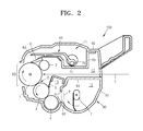
- FIG. 2 is a schematic view showing the configuration of a developing device included in the electrophotographic image forming apparatus of FIG. 1 , according to an embodiment of the present general inventive concept.
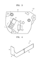
- FIG. 3 is a side view of the developing device illustrated in FIG. 2 , according to an embodiment of the present general inventive concept
- FIG. 4 is a perspective view of a blocking member, according to an embodiment of the present general inventive concept
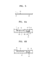
- FIG. 5 is a side view of a blocking member in which a bending line is formed, according to an embodiment of the present general inventive concept
- FIGS. 6A, 6B , and 6C are cross-sectional views taken along line A-A' of FIG. 4 , according to an embodiment of the present general inventive concept;
- FIG. 7 is a perspective view of the blocking member inserted in a housing via an insertion hole formed in sidewall of a housing, according to an embodiment of the present general inventive concept
- FIG. 8 is a cross-sectional view of the developing device in an upright position in order to recover toner from a developing portion to a toner storage area after a performance test is performed, according to an embodiment of the present general inventive concept;
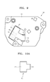
- FIG. 9 is a side view of the developing device in which a bent portion of the blocking member covers a communication portion, according to an embodiment of the present general inventive concept.
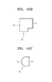
- FIGS. 10A-10C illustrate shapes of blocking members according to embodiments of the present general inventive concept.
- FIG. 1 illustrates a configuration of an electrophotographic image forming apparatus, according to an embodiment of the present general inventive concept
- FIG. 2 is a schematic view showing the configuration of a developing device 100 included in the electrophotographic image forming apparatus of FIG. 1 , according to an embodiment of the present general inventive concept.
- the developing device 100 of according to the present embodiment is an integrated developing device including a photoconductive drum 1 and a developing roller 3.
- the photoconductive drum 1 is an example of a photoconductor on which an electrostatic latent image is formed, and includes a photoconductive layer formed around an outer circumference of a cylindrical metal pipe.
- a charging roller 2 is an example of a charger that charges the surface of the photoconductive drum 1 to a uniform potential.
- a charging bias voltage is applied to the charging roller 2.
- a corona charger (not shown) may be used instead of the charging roller 2.
- the developing roller 3 supplies toner to the electrostatic latent image formed on the surface of the photoconductive drum 1 in order to develop the electrostatic latent image.
- the electrophotographic image forming apparatus uses a contact developing technique in which the developing roller 3 and the photoconductive drum 1 contact each other, thereby forming a development nip D.
- the developing roller 3 may include an elastic layer (not shown) formed around an outer circumference of a conductive metal core (not shown).
- a developing bias voltage is applied to the developing roller 3
- the toner is transferred via the development nip D to the electrostatic latent image formed on the surface of the photoconductive drum 1 and attached thereto.
- a non-contact developing technique is used, the surface of the developing roller 3 and the surface of the photoconductive drum 1 are separated from each other at intervals of about, for example, several microns.
- the developing device 100 may further include a supply roller 4 that attaches the toner to the developing roller 3.
- a supply bias voltage may be applied to the supply roller 4 so as to attach the toner to the developing roller 3.
- Reference numeral 5 denotes a regulator that regulates the amount of the toner attached to the surface of the developing roller 3.
- the regulator 5 may be a regulating blade of which front end contacts the developing roller 3 with a predetermined pressure.
- Member 6 may be a cleaning blade of which front end contacts the surface of the photoconductive drum 1.
- waste toner the foreign substance removed from the surface of the photoconductive drum 1 is referred to as waste toner.
- the developing device 100 includes a toner container, or toner storage area 10 and a waste toner container or waste toner storage area 11.
- the waste toner that is removed from the surface of the photoconductive drum 1 is stored in the waste toner storage area 11.
- the developing device 100 of FIG. 2 is a developing device that uses a one-component developing agent, and the toner is stored in the toner storage area 10.
- An agitator 7 is installed in the toner storage area 10. The agitator 7 transports the toner to the developing roller 3 and may agitate the toner to frictionally charge it to a predetermined potential. Although one agitator 7 is shown in FIG. 2 , the scope of the present general inventive concept is not limited to a single agitator 7.
- An appropriate number of agitators 7 may be installed in appropriate positions in the toner storage area 10 so as to effectively supply the toner to the developing roller 3 in consideration of the volume or shape of the toner storage area 10.
- the agitator 7 may include one or a plurality of flexible film-shaped agitation wings formed on a rotation axis. Although not shown, the agitator 7 may be an auger including spiral-shaped agitation wings.
- the developing roller 3 may include a magnet disposed in a rotating sleeve.
- the carrier is attached to the outer circumference of the developing roller 3 due to a magnetic force of the magnet, and the toner is attached to the carrier due to an electrostatic force, thereby forming a magnetic brush including the carrier and the toner around the outer circumference of the developing roller 3. Due to the developing bias voltage applied to the developing roller 3, only the toner is moved to the electrostatic latent image formed on the surface of the photoconductive drum 1.
- the regulator 5 regulates the height of the magnetic brush that is separated from the surface of the developing roller 3 at a predetermined distance and is formed around the outer circumference of the developing roller 3.
- the agitator 7 transports the carrier and the toner to the developing roller 3 and agitates the carrier and the toner to frictionally charge the toner to a predetermined potential.
- a housing 90 of the developing device 100 may include a lower frame 91 and an upper frame 92. Part of the outer circumference of the photoconductive drum 1 is exposed to the outside of the housing 90 via an opening 93.
- First and second barrier walls 94 and 95 may be disposed in the housing 90.
- the lower frame 91 and the first barrier wall 94 constitute the toner storage area 10
- the upper frame 92 and the second barrier wall 95 constitutes the waste toner storage area 11.
- the first barrier wall 94 and the second barrier wall 95 are separated from each other and define an optical path 12 along which light L scanned by an optical scanning unit (200 of FIG. 1 ) is incident on the photoconductive drum 1, in order to expose the photoconductive drum 1 between the first and second barrier walls 94 and 95.
- a waste toner transporting member 60 is installed at the waste toner storage area 11.
- the waste toner transporting member 60 is connected to an eccentricity portion 71 that is disposed eccentrically from a rotation center of a rotation member 70.
- the waste toner transporting member 60 makes a reciprocating motion and transports the waste toner that is removed from the photoconductive drum 1 into the waste toner storage area 11.
- the waste toner transporting member may include an end portion 64 adjacent to the cleaning blade 6 to receive the waste toner from the cleaning blade 6 and to transfer the waste toner to the waste toner storage area 11.
- the developing device 100 is mounted into a main body 700 of the electrophotographic image forming apparatus through a door 701.
- the optical scanning unit 200 scans light modulated according to image information onto the photoconductive drum 1 that has been charged to a uniform potential.
- a laser scanning unit (LSU) that scans light emitted from a laser diode onto the photoconductive drum 1 by deflecting the light in a main scanning direction by using a polygon mirror may be used as the optical scanning unit 200.
- the transfer roller 300 which is an example of a transfer unit, is located to face the surface of the photoconductive drum 1, and forms a transfer nip.
- a transfer bias voltage is applied to the transfer roller 300 so as to transfer a toner image developed on the surface of the photoconductive drum 1 to the recording medium P.
- a corona transfer unit may be used instead of the transfer roller 300.
- the toner image transferred to the surface of the recording medium P by the transfer roller 300 remains adhered to the surface of the recording medium P due to electrostatic attraction.
- the fixing unit or fusing unit 400 applies heat and pressure to fix the toner image to the recording medium P, thereby forming a permanent printed image on the recording medium P.
- a method of forming an image using the electrophotographic image forming apparatus having the above configuration will now be briefly described.
- a charging bias voltage is applied to the charging roller 2
- the photoconductive drum 1 is charged to a uniform potential.
- the optical scanning unit 200 scans light modulated according to image information onto the photoconductive drum 1 through the optical path 12 formed on the developing device 100, thereby forming an electrostatic latent image on the surface of the photoconductive drum 1.
- the toner is transported to the supply roller 4 via the agitator 7, and the supply roller 4 attaches the toner to the surface of the developing roller 3.
- the regulator 5 forms a toner layer having a uniform thickness on the surface of the developing roller 3.
- a developing bias voltage is applied to the developing roller 3.
- the toner that is moved to the development nip D as the developing roller 3 rotates is transferred and attached to the electrostatic latent image, which is formed on the surface of the photoconductive drum 1, due to the developing bias voltage, so that a visible toner image is formed on the surface of the photoconductive drum 1.
- the recording medium P picked up from a recording medium tray 501 by a pick-up roller 502 is transported to the transfer nip between the transfer roller 300 and the photoconductive drum 1 by a transporting roller 503.
- a transfer bias voltage is applied to the transfer roller 300, the toner image formed on the photosensitive drum 1 is transferred to the recording medium P by electrostatic attraction.
- the toner image transferred to the recording medium P is fixed to the recording medium P by heat and pressure applied from the fixing unit 400, and thus, the printing is completed.
- the recording medium P is discharged to the outside by a discharge roller 504. Toner remaining on the surface of the photoconductive drum 1 without being transferred to the recording medium P is removed by a cleaning member 6 and collected in a waste toner storage area 11.
- the developing device 100 is replaceable, and thus may be handled separately from the main body 700 of the electrophotographic image forming apparatus.
- a developing portion 13 in which the developing roller 3 is installed is connected to the toner storage area 10 via a toner supply window 8.
- the toner may leak through the opening 93 during a distribution or handling process.
- the toner supply window 8 is closed using a blocking member 80 so that the toner storage area 10 and the developing portion 13 may be separated from each other.
- the blocking member 80 is removed before the developing device 100 is mounted on the main body 700, so that the toner storage area 10 and the developing portion 13 may be connected to each other via the toner supply window 8. Then, the toner contained in the toner storage area 10 may be supplied to the developing portion 13.
- a barrier wall member (not shown) to which a blocking film (not shown) is attached is fused on the toner supply window 8, and part of the blocking film is exposed to the outside of the housing 90.
- the toner storage area 10 and the developing portion 13 are connected to each other by removing the blocking film by pulling out the exposed part of the blocking film.
- toner for a performance test of the developing device needs to be loaded into the developing portion 13 so as to carry out the performance test of the developing device.
- a loading hole (not shown) through which the toner for the performance test is loaded into the developing portion 13 needs to be formed in the housing 90, and after the performance test is completed, a process of closing or sealing the loading hole needs to be performed.
- the blocking member 80 is inserted in the inside of the housing 90 from the outside of the housing 90, thereby closing the toner supply window 8.
- a pair of rails 9 are disposed on the toner supply window 8 and extend in a lengthwise direction of the developing roller 3, or along the length axis F illustrated in FIG. 7 .
- the rails 9 extend along upper and lower edges of the toner supply window 8.
- the rails 9 include a groove recessed between two raised portions, and the ends of the blocking portion 81 can slide in the lengthwise directions F1 and F2 along the groove to block the toner supply window 8.
- an insertion hole 40 is formed in sidewall (96 of FIG.
- the blocking member 80 includes a blocking portion 81 that is inserted in the rails 9 and closes the toner supply window 8, and a bent portion 82 that is bent from the blocking portion 81.
- the bent portion 82 is disposed at the outside of the housing 90 while the blocking portion 81 is inserted in the rails 9.
- the bent portion 82 may serve as a handle when the blocking portion 81 is removed from the rails 9.
- the blocking member 80 may be manufactured by cutting a flexible board that may be elastically bent in a desired form. After the board is cut in the desired form, the bent portion 82 may be bent parallel to sidewall 96 of the housing 90, as illustrated in FIG. 4 . In addition, after the board is cut in the desired form, a bending line 83 may be formed so that the bent portion 82 may be bent with respect to the blocking portion 81 along the bending line 83, as illustrated in FIG. 5 . The bending line 83 may be formed to be recessed from the surface of the blocking member 80, for example. In this case, after the blocking portion 81 is inserted in the rails 9, the bent portion 82 may be bent parallel to the sidewall 96 of the housing 90 along the bending line 83. Manufacturing of the blocking member 80 is not limited to the above-described method, and the blocking member 80 may be manufactured using various methods including plastic injection molding or the like.
- a securing portion 41 is disposed on the sidewall 96.
- the securing portion 41 secures the bent portion 82 on the sidewall 96 while the blocking portion 81 is inserted in the rails 9 and the bent portion 82 is bent in a direction parallel to the sidewall 96.
- the securing portion 41 may be in the form of a protrusion so that the securing portion 41 may be caught in edges 84 of the bent portion 82.
- a communication portion 50 that is electrically connected to the main body 700 after the developing device 100 was mounted on the main body 700 of the electrophotographic image forming apparatus and transmits information about the developing device 100 to the main body 700 may be disposed on the sidewall 96 of the housing 90.
- the communication portion 50 may be a circuit board including a memory (not shown) in which information such as a model name or the like of the developing device 100 is recorded, and a plurality of electrical contact point portions 51 for electrically connecting the communication portion 50 to the main body 700.
- the sidewall 96 may include a first recessed portion 96a, and the communication portion 50 may be located within the first recessed portion 96a.
- the sidewall 96 may include a raised portion 96b and a second recessed portion 96c located between the raised portion 96b and the insertion hole 40.
- the bent portion 82 of the blocking member 80 may be bent to be parallel with each of the recessed portions 96a and 96c and the raised portion 96b.
- the bent portion 82 may be bent such that a surface of the bent portion 82 directly contacts the raised portion 96b.
- the raised portion 96b may be raised with respect to the recessed portions 96a and 96c, the raised portion 96b may be recessed with respect to an upper surface of the sidewall 96, such that when the bent portion 82 of the blocking member 80 is bent, an end of the bent portion 82 may be positioned between the securing portion 41 and the recessed portion 96a while staying parallel to the recessed portion 96a.
- the recessed portion 96c may be of a sufficient size to receive the sealing member 42.
- an upper surface of the sealing member 42 may be flush with an upper surface of the raised portion 96b of the sidewall 96.
- the bent portion 82 may also serve as a protection portion that covers and protects the communication portion 50.
- the bent portion 82 may cover an upper portion of the communication portion 50 while being bent parallel to the sidewall 96 of the housing 90.
- the securing portion 41 may secure the bent portion 82 on the sidewall 96 when the bent portion 82 covers the communication portion 50 so that a predetermined force is required to remove the blocking member 80 from the developing unit 100.
- the securing portion 41 may be designed to overlap the edge 84 of the bent portion 82 sufficiently so that a small shaking force or a gravity force are not sufficient to remove the blocking member 80 from the developer 100, but an intentional force may be required.
- the developing device 100 may further include a sealing member 42 that prevents leakage of the toner via the insertion hole 40.
- the sealing member 42 may be an elastic member such as a sponge or the like.
- the sealing member 42 may be attached to the sidewall 96 of the housing 90 by using a double-sided tape so as to cover at least part of the insertion hole 40.
- the blocking member 80 may be inserted in the housing 90 via the insertion hole 40 while pushing the sealing member 42.
- the toner leakage prevention member 42 presses against the blocking member 80 to prevent any leakage of toner.
- FIG. 6B when the blocking member 80 is removed from the insertion hole 40, the elastic nature of the toner leakage prevention member 42 causes the toner leakage prevention member 42 to expand to cover the insertion hole 40 to prevent toner from leaking from the insertion hole 40.
- the sealing member 42 may have a curved or slanted shape at an end where the blocking member 80 enters the insertion hole 40 to facilitate the entry of the blocking member 80 into the insertion hole 40. Since the blocking member 80 may be repeatedly inserted into and removed from the insertion hole 40, as necessary, the curved end of the sealing member 42 may allow for easier insertion of the blocking member 80 into the insertion hole 40 while providing protection from leaking toner from the hole 40.
- the developing device 100 may further include inner sidewall 97, and the sidewall 96 may be combined with the inner sidewall 97.
- the insertion hole 40 is formed through the sidewall 96 and the inner sidewall 97.
- the sidewall 96 may be a support plate that supports the developing roller 3, the charging roller 2 or the like, which is installed at the developing device 100.
- the toner is charged in the toner storage area 10 while the blocking member 80 is not installed at the developing device 100 after the developing device 100 has been manufactured. Then, as illustrated in FIG. 2 , the toner storage area 10 is connected to the developing portion 13 via the toner supply window 8.
- the performance test of the developing device 100 is performed in this state. When the performance test is completed, as illustrated in FIG. 7 , the blocking member 80 is inserted in the rails 9 through the insertion hole 40. In this case, the toner does not need to remain on the developing portion 13. To this end, as illustrated in FIG. 8 , the blocking member 80 may be inserted in the rails 9 while the developing portion 13 is oriented upwards and the toner contained in the developing portion 13 is recovered to the toner storage area 10.
- the developer may be oriented to that the opening 93 faces the direction B1 and the toner storage area 10 is oriented in the direction B2 with respect to the opening 93.
- the toner supply window 8 is closed so that the toner storage area 10 and the developing portion 13 may be isolated from each other.
- the bent portion 82 is disposed parallel to the sidewall 96 of the housing 90, and the edges 84 of the bent portion 82 are caught in the securing portion 41, thereby securing the bent portion 82 on the sidewall 96. Then, as illustrated in FIG. 9 , the bent portion 82 is secured on the sidewall 96 while covering the communication portion 50, thereby preventing damage of the communication portion 50 due to physical or electrical shock during the distribution process.
- the bent portion 82 is released from the securing portion 41 before the developing device 100 is mounted on the main body 700 of the electrophotographic image forming apparatus, and the bent portion 82 is grasped and pulled out in an opposite direction to a direction in which the bent portion 82 is inserted, and the blocking member 80 is removed from the housing 90. Then, the toner storage area 10 and the developing portion 13 are connected to each other via the toner supply window 8. Next, when the developing device 100 is mounted on the main body 700 of the electrophotographic image forming apparatus, the communication portion 50 may be electrically connected to the main body 700 and may transmit information about the developing device 100 to the main body 700.
- the blocking member 80 may have any shape appropriate to a particular developing unit 100.
- the bent portion 82 is located at an angle perpendicular to the blocking portion 81.
- the bent portion 82 may be positioned at any angle with respect to the blocking portion 81.
- the blocking portion 81 may be rotated at a non-right angle with respect to the blocking portion 81.
- the blocking portion 81 may be bent at the bending line 83 to an angle less than or more than ninety degrees according to the particular developing unit.
- FIG. 10B illustrates a bent portion 82 that has a tab that extends in only one direction (downward).
- the bent portion 82 may have any number of tabs of any shapes.
- the bent portion 82 may be curved or rounded.
- the communication portion 50 is covered by the bent portion 82 when the blocking member 80 is inserted into the insertion hole 40 and is exposed when the blocking member 80 is removed from the insertion hole 40.
- the blocking member 80 when the blocking member 80 is inserted into the insertion hole 40, the blocking member 80 may be substantially straight, and the bent portion 82 may then be bent to cover the communication portion 50. In other words, the bent portion 82 may be bent either before or after the blocking portion 80 is inserted into the insertion hole 40.
- the blocking portion 81 no longer closes the toner supply window 8 so that toner may flow between the toner storage area 10 and the developing portion 13, and the bent portion 82 no longer covers the communication portion 50 so that electrical contact points 51 may contact electrical contact points (not shown) of the main body 700 to allow the developing unit 100 to communicate with the main unit 700.
- a monochromic electrophotographic image forming apparatus including one developing device 100 has been illustrated in the previous embodiments, the scope of the present general inventive concept is not limited thereto.
- four developing devices 100 in which toners having colors such as cyan (C), magenta (M), yellow (Y), and black (K) are contained, may be employed.
Landscapes
- Physics & Mathematics (AREA)
- General Physics & Mathematics (AREA)
- Engineering & Computer Science (AREA)
- Computer Vision & Pattern Recognition (AREA)
- Dry Development In Electrophotography (AREA)
Abstract
Description
- This application claims the benefit of Korean Patent Application No.
10-2010-0005758, filed on January 21, 2010 - The present general inventive concept relates to a developing device and an electrophotographic image forming apparatus including the developing device.
- An electrophotographic image forming apparatus prints images on a recording medium through several processes, which may include irradiating light modulated according to image information onto a photoconductor to form an electrostatic latent image on the surface of the photoconductor, supplying toner to the electrostatic latent image to develop the electrostatic latent image into a visible toner image, and transferring and fixing the toner image onto the recording medium. The electrophotographic image forming apparatus includes a developing device which contains toner.
- The photoconductor and the toner may be provided in the form of a replaceable cartridge that is commonly referred to as a 'developing device'. When the toner in the developing device is exhausted, the developing device may be removed from the electrophotographic image forming apparatus and replaced with a new developing device.
- According to the present invention there is provided an apparatus and method as set forth in the appended claims. Other features of the invention will be apparent from the dependent claims, and the description which follows.
- A toner storage area and a developing portion need to be separated from each other so that toner in a developing device does not leak before the developing device is installed in an electrophotographic image forming apparatus.
- The present general inventive concept provides a developing device in which the toner storage area and the developing portion are easily separated from each other and an electrophotographic image forming apparatus including the developing device.
- According to an aspect of the present general inventive concept, there is provided a developing device to be attached to and detached from a main body of an electrophotographic image forming apparatus, the developing device comprising: a housing that defines a toner storage area to store toner and a developing portion having a developing roller, wherein the housing further includes an opening that defines a toner supply window to connect the toner storage area to the developing portion, a pair of rails adjacent to the toner supply window and extending in an end-to-end lengthwise direction of the developing roller, and an insertion hole on a sidewall of the housing corresponding to a location of the pair of rails; and the developing device further comprises a blocking member comprising a blocking portion, such that the toner supply window is open when the blocking member is removed from the pair of rails and the toner supply window is closed when the blocking member is inserted in the pair of rails from an outside of the housing.
- The blocking member may further include a bent portion extending from the blocking portion and disposed at outside of the housing when the blocking portion is inserted in the rails.
- The bent portion may be bent in a direction parallel to the sidewall of the housing. The developing device may further include a communication portion disposed on the sidewall of the housing and electrically connected to the main body when the developing device is mounted on the main body, wherein the blocking portion covers the communication portion when the blocking portion is inserted in the rails. The developing device may further include a securing portion disposed on the sidewall of the housing and securing the bent portion when the bent portion covers the communication portion.
- The bent portion may be divided from the blocking portion along a bending line and may be bend able in the direction parallel to the sidewall of the housing. The developing device may further include a communication portion disposed on the sidewall of the housing and electrically connected to the main body when the developing device is mounted on the main body, wherein the bent portion is bent parallel to the sidewall of the housing along the bending line and covers the communication portion when the blocking portion is inserted in the rails. The developing device may further include a securing portion disposed on the sidewall of the housing and securing the bent portion when the bent portion covers the communication portion.
- The developing may further include a sealing member disposed on the sidewall of the housing and formed of an elastic material to cover the insertion hole.
- The developing device may further comprises a communication portion disposed on sidewall of the housing to electrically connect to the main body when the developing device is mounted on the main body, and the blocking member further comprises a protection portion covering the communication portion when the blocking portion is inserted in the rails.
- The protection portion may be bent in a direction parallel to the sidewall of the housing from the blocking portion so as to cover the communication portion. The protection portion may be divided from the blocking portion along a bending line and may be bent in the direction that is parallel to the sidewall of the housing along the bending line and may cover the communication portion. The developing device may further include a securing portion disposed on the sidewall of the housing and securing the bent portion when the protection portion covers the communication portion.
- The developing device may further include a sealing member disposed on the sidewall of the housing and formed of an elastic material for covering the insertion hole.
- According to another aspect of the present general inventive concept, there may be provided an electrophotographic image forming apparatus including the above-described developing device.
- The above and other features and advantages of the present general inventive concept will become more apparent by describing in detail exemplary embodiments thereof with reference to the attached drawings in which:
-
FIG. 1 is a schematic view showing the configuration of an electrophotographic image forming apparatus, according to an embodiment of the present general inventive concept. -
FIG. 2 is a schematic view showing the configuration of a developing device included in the electrophotographic image forming apparatus ofFIG. 1 , according to an embodiment of the present general inventive concept. -
FIG. 3 is a side view of the developing device illustrated inFIG. 2 , according to an embodiment of the present general inventive concept; -
FIG. 4 is a perspective view of a blocking member, according to an embodiment of the present general inventive concept; -
FIG. 5 is a side view of a blocking member in which a bending line is formed, according to an embodiment of the present general inventive concept; -
FIGS. 6A, 6B , and6C are cross-sectional views taken along line A-A' ofFIG. 4 , according to an embodiment of the present general inventive concept; -
FIG. 7 is a perspective view of the blocking member inserted in a housing via an insertion hole formed in sidewall of a housing, according to an embodiment of the present general inventive concept; -
FIG. 8 is a cross-sectional view of the developing device in an upright position in order to recover toner from a developing portion to a toner storage area after a performance test is performed, according to an embodiment of the present general inventive concept; -
FIG. 9 is a side view of the developing device in which a bent portion of the blocking member covers a communication portion, according to an embodiment of the present general inventive concept; and -
FIGS. 10A-10C illustrate shapes of blocking members according to embodiments of the present general inventive concept. - The present general inventive concept will now be described more fully with reference to the accompanying drawings, in which exemplary embodiments of the present general inventive concept are shown. Like numerals refer to like elements throughout.
-
FIG. 1 illustrates a configuration of an electrophotographic image forming apparatus, according to an embodiment of the present general inventive concept, andFIG. 2 is a schematic view showing the configuration of a developingdevice 100 included in the electrophotographic image forming apparatus ofFIG. 1 , according to an embodiment of the present general inventive concept. The developingdevice 100 of according to the present embodiment is an integrated developing device including aphotoconductive drum 1 and a developingroller 3. - Referring to
FIG. 2 , thephotoconductive drum 1 is an example of a photoconductor on which an electrostatic latent image is formed, and includes a photoconductive layer formed around an outer circumference of a cylindrical metal pipe. Acharging roller 2 is an example of a charger that charges the surface of thephotoconductive drum 1 to a uniform potential. A charging bias voltage is applied to thecharging roller 2. A corona charger (not shown) may be used instead of thecharging roller 2. The developingroller 3 supplies toner to the electrostatic latent image formed on the surface of thephotoconductive drum 1 in order to develop the electrostatic latent image. The electrophotographic image forming apparatus according to the present embodiment uses a contact developing technique in which the developingroller 3 and thephotoconductive drum 1 contact each other, thereby forming a development nip D. In this case, the developingroller 3 may include an elastic layer (not shown) formed around an outer circumference of a conductive metal core (not shown). When a developing bias voltage is applied to the developingroller 3, the toner is transferred via the development nip D to the electrostatic latent image formed on the surface of thephotoconductive drum 1 and attached thereto. When a non-contact developing technique is used, the surface of the developingroller 3 and the surface of thephotoconductive drum 1 are separated from each other at intervals of about, for example, several microns. - The developing
device 100 may further include asupply roller 4 that attaches the toner to the developingroller 3. A supply bias voltage may be applied to thesupply roller 4 so as to attach the toner to the developingroller 3.Reference numeral 5 denotes a regulator that regulates the amount of the toner attached to the surface of the developingroller 3. Theregulator 5 may be a regulating blade of which front end contacts the developingroller 3 with a predetermined pressure.Member 6 may be a cleaning blade of which front end contacts the surface of thephotoconductive drum 1. Hereinafter, the foreign substance removed from the surface of thephotoconductive drum 1 is referred to as waste toner. - The developing
device 100 includes a toner container, ortoner storage area 10 and a waste toner container or wastetoner storage area 11. The waste toner that is removed from the surface of thephotoconductive drum 1 is stored in the wastetoner storage area 11. The developingdevice 100 ofFIG. 2 is a developing device that uses a one-component developing agent, and the toner is stored in thetoner storage area 10. Anagitator 7 is installed in thetoner storage area 10. Theagitator 7 transports the toner to the developingroller 3 and may agitate the toner to frictionally charge it to a predetermined potential. Although oneagitator 7 is shown inFIG. 2 , the scope of the present general inventive concept is not limited to asingle agitator 7. An appropriate number ofagitators 7 may be installed in appropriate positions in thetoner storage area 10 so as to effectively supply the toner to the developingroller 3 in consideration of the volume or shape of thetoner storage area 10. Theagitator 7 may include one or a plurality of flexible film-shaped agitation wings formed on a rotation axis. Although not shown, theagitator 7 may be an auger including spiral-shaped agitation wings. - When a two-component developing agent including the toner and a carrier is used as the developing agent, a magnetic carrier and the toner are contained in the
toner storage area 10. In this case, the developingroller 3 may include a magnet disposed in a rotating sleeve. The carrier is attached to the outer circumference of the developingroller 3 due to a magnetic force of the magnet, and the toner is attached to the carrier due to an electrostatic force, thereby forming a magnetic brush including the carrier and the toner around the outer circumference of the developingroller 3. Due to the developing bias voltage applied to the developingroller 3, only the toner is moved to the electrostatic latent image formed on the surface of thephotoconductive drum 1. Theregulator 5 regulates the height of the magnetic brush that is separated from the surface of the developingroller 3 at a predetermined distance and is formed around the outer circumference of the developingroller 3. Theagitator 7 transports the carrier and the toner to the developingroller 3 and agitates the carrier and the toner to frictionally charge the toner to a predetermined potential. - A
housing 90 of the developingdevice 100 may include alower frame 91 and anupper frame 92. Part of the outer circumference of thephotoconductive drum 1 is exposed to the outside of thehousing 90 via anopening 93. First andsecond barrier walls housing 90. Thelower frame 91 and thefirst barrier wall 94 constitute thetoner storage area 10, and theupper frame 92 and thesecond barrier wall 95 constitutes the wastetoner storage area 11. Thefirst barrier wall 94 and thesecond barrier wall 95 are separated from each other and define anoptical path 12 along which light L scanned by an optical scanning unit (200 ofFIG. 1 ) is incident on thephotoconductive drum 1, in order to expose thephotoconductive drum 1 between the first andsecond barrier walls - A waste
toner transporting member 60 is installed at the wastetoner storage area 11. The wastetoner transporting member 60 is connected to aneccentricity portion 71 that is disposed eccentrically from a rotation center of arotation member 70. As therotation member 70 rotates, the wastetoner transporting member 60 makes a reciprocating motion and transports the waste toner that is removed from thephotoconductive drum 1 into the wastetoner storage area 11. According to one embodiment, the waste toner transporting member may include anend portion 64 adjacent to thecleaning blade 6 to receive the waste toner from thecleaning blade 6 and to transfer the waste toner to the wastetoner storage area 11. - Referring to
FIG. 1 , the developingdevice 100 is mounted into amain body 700 of the electrophotographic image forming apparatus through adoor 701. Theoptical scanning unit 200 scans light modulated according to image information onto thephotoconductive drum 1 that has been charged to a uniform potential. For example, a laser scanning unit (LSU) that scans light emitted from a laser diode onto thephotoconductive drum 1 by deflecting the light in a main scanning direction by using a polygon mirror may be used as theoptical scanning unit 200. - The
transfer roller 300, which is an example of a transfer unit, is located to face the surface of thephotoconductive drum 1, and forms a transfer nip. A transfer bias voltage is applied to thetransfer roller 300 so as to transfer a toner image developed on the surface of thephotoconductive drum 1 to the recording medium P. - A corona transfer unit may be used instead of the
transfer roller 300. The toner image transferred to the surface of the recording medium P by thetransfer roller 300 remains adhered to the surface of the recording medium P due to electrostatic attraction. The fixing unit or fusingunit 400 applies heat and pressure to fix the toner image to the recording medium P, thereby forming a permanent printed image on the recording medium P. - A method of forming an image using the electrophotographic image forming apparatus having the above configuration will now be briefly described. When a charging bias voltage is applied to the charging
roller 2, thephotoconductive drum 1 is charged to a uniform potential. Theoptical scanning unit 200 scans light modulated according to image information onto thephotoconductive drum 1 through theoptical path 12 formed on the developingdevice 100, thereby forming an electrostatic latent image on the surface of thephotoconductive drum 1. The toner is transported to thesupply roller 4 via theagitator 7, and thesupply roller 4 attaches the toner to the surface of the developingroller 3. Theregulator 5 forms a toner layer having a uniform thickness on the surface of the developingroller 3. A developing bias voltage is applied to the developingroller 3. The toner that is moved to the development nip D as the developingroller 3 rotates is transferred and attached to the electrostatic latent image, which is formed on the surface of thephotoconductive drum 1, due to the developing bias voltage, so that a visible toner image is formed on the surface of thephotoconductive drum 1. The recording medium P picked up from arecording medium tray 501 by a pick-uproller 502 is transported to the transfer nip between thetransfer roller 300 and thephotoconductive drum 1 by a transportingroller 503. When a transfer bias voltage is applied to thetransfer roller 300, the toner image formed on thephotosensitive drum 1 is transferred to the recording medium P by electrostatic attraction. The toner image transferred to the recording medium P is fixed to the recording medium P by heat and pressure applied from the fixingunit 400, and thus, the printing is completed. The recording medium P is discharged to the outside by adischarge roller 504. Toner remaining on the surface of thephotoconductive drum 1 without being transferred to the recording medium P is removed by a cleaningmember 6 and collected in a wastetoner storage area 11. - The developing
device 100 is replaceable, and thus may be handled separately from themain body 700 of the electrophotographic image forming apparatus. A developingportion 13 in which the developingroller 3 is installed is connected to thetoner storage area 10 via atoner supply window 8. When thetoner storage area 10 and the developingportion 13 are connected to each other, the toner may leak through theopening 93 during a distribution or handling process. Thus, as illustrated inFIG. 2 , thetoner supply window 8 is closed using a blockingmember 80 so that thetoner storage area 10 and the developingportion 13 may be separated from each other. The blockingmember 80 is removed before the developingdevice 100 is mounted on themain body 700, so that thetoner storage area 10 and the developingportion 13 may be connected to each other via thetoner supply window 8. Then, the toner contained in thetoner storage area 10 may be supplied to the developingportion 13. - In a conventional developing device, a barrier wall member (not shown) to which a blocking film (not shown) is attached is fused on the
toner supply window 8, and part of the blocking film is exposed to the outside of thehousing 90. In the conventional developing device, thetoner storage area 10 and the developingportion 13 are connected to each other by removing the blocking film by pulling out the exposed part of the blocking film. Thus, in the conventional developing device, a process of attaching the blocking film to the barrier wall member and a process of fusing the barrier wall member on the inside of thehousing 90 need to be performed, and thus the manufacturing costs increase. In addition, since thetoner storage area 10 and the developingportion 13 are completely separated from each other, toner for a performance test of the developing device needs to be loaded into the developingportion 13 so as to carry out the performance test of the developing device. To this end, a loading hole (not shown) through which the toner for the performance test is loaded into the developingportion 13 needs to be formed in thehousing 90, and after the performance test is completed, a process of closing or sealing the loading hole needs to be performed. - In the developing
device 100 according to the present general inventive concept, the blockingmember 80 is inserted in the inside of thehousing 90 from the outside of thehousing 90, thereby closing thetoner supply window 8. Referring toFIG. 2 , a pair of rails 9 are disposed on thetoner supply window 8 and extend in a lengthwise direction of the developingroller 3, or along the length axis F illustrated inFIG. 7 . The rails 9 extend along upper and lower edges of thetoner supply window 8. The rails 9 include a groove recessed between two raised portions, and the ends of the blockingportion 81 can slide in the lengthwise directions F1 and F2 along the groove to block thetoner supply window 8. Referring toFIG. 3 , aninsertion hole 40 is formed in sidewall (96 ofFIG. 3 ) of thehousing 90 to be aligned with the rails 9. Referring toFIG. 4 , the blockingmember 80 includes a blockingportion 81 that is inserted in the rails 9 and closes thetoner supply window 8, and abent portion 82 that is bent from the blockingportion 81. Thebent portion 82 is disposed at the outside of thehousing 90 while the blockingportion 81 is inserted in the rails 9. Thebent portion 82 may serve as a handle when the blockingportion 81 is removed from the rails 9. - The blocking
member 80 may be manufactured by cutting a flexible board that may be elastically bent in a desired form. After the board is cut in the desired form, thebent portion 82 may be bent parallel to sidewall 96 of thehousing 90, as illustrated inFIG. 4 . In addition, after the board is cut in the desired form, abending line 83 may be formed so that thebent portion 82 may be bent with respect to the blockingportion 81 along the bendingline 83, as illustrated inFIG. 5 . The bendingline 83 may be formed to be recessed from the surface of the blockingmember 80, for example. In this case, after the blockingportion 81 is inserted in the rails 9, thebent portion 82 may be bent parallel to thesidewall 96 of thehousing 90 along the bendingline 83. Manufacturing of the blockingmember 80 is not limited to the above-described method, and the blockingmember 80 may be manufactured using various methods including plastic injection molding or the like. - Referring to
FIGS. 3 and6A , a securingportion 41 is disposed on thesidewall 96. The securingportion 41 secures thebent portion 82 on thesidewall 96 while the blockingportion 81 is inserted in the rails 9 and thebent portion 82 is bent in a direction parallel to thesidewall 96. The securingportion 41 may be in the form of a protrusion so that the securingportion 41 may be caught inedges 84 of thebent portion 82. - A
communication portion 50 that is electrically connected to themain body 700 after the developingdevice 100 was mounted on themain body 700 of the electrophotographic image forming apparatus and transmits information about the developingdevice 100 to themain body 700 may be disposed on thesidewall 96 of thehousing 90. For example, thecommunication portion 50 may be a circuit board including a memory (not shown) in which information such as a model name or the like of the developingdevice 100 is recorded, and a plurality of electricalcontact point portions 51 for electrically connecting thecommunication portion 50 to themain body 700. - The
sidewall 96 may include a first recessedportion 96a, and thecommunication portion 50 may be located within the first recessedportion 96a. Thesidewall 96 may include a raisedportion 96b and a second recessedportion 96c located between the raisedportion 96b and theinsertion hole 40. Thebent portion 82 of the blockingmember 80 may be bent to be parallel with each of the recessedportions portion 96b. Thebent portion 82 may be bent such that a surface of thebent portion 82 directly contacts the raisedportion 96b. Although the raisedportion 96b may be raised with respect to the recessedportions portion 96b may be recessed with respect to an upper surface of thesidewall 96, such that when thebent portion 82 of the blockingmember 80 is bent, an end of thebent portion 82 may be positioned between the securingportion 41 and the recessedportion 96a while staying parallel to the recessedportion 96a. - The recessed
portion 96c may be of a sufficient size to receive the sealingmember 42. In other words, an upper surface of the sealingmember 42 may be flush with an upper surface of the raisedportion 96b of thesidewall 96. - In the developing
device 100 according to the present general inventive concept, thebent portion 82 may also serve as a protection portion that covers and protects thecommunication portion 50. In detail, as illustrated inFIG. 6 , thebent portion 82 may cover an upper portion of thecommunication portion 50 while being bent parallel to thesidewall 96 of thehousing 90. The securingportion 41 may secure thebent portion 82 on thesidewall 96 when thebent portion 82 covers thecommunication portion 50 so that a predetermined force is required to remove the blockingmember 80 from the developingunit 100. For example, the securingportion 41 may be designed to overlap theedge 84 of thebent portion 82 sufficiently so that a small shaking force or a gravity force are not sufficient to remove the blockingmember 80 from thedeveloper 100, but an intentional force may be required. - The developing
device 100 according to the present general inventive concept may further include a sealingmember 42 that prevents leakage of the toner via theinsertion hole 40. The sealingmember 42 may be an elastic member such as a sponge or the like. The sealingmember 42 may be attached to thesidewall 96 of thehousing 90 by using a double-sided tape so as to cover at least part of theinsertion hole 40. The blockingmember 80 may be inserted in thehousing 90 via theinsertion hole 40 while pushing the sealingmember 42. - As illustrated in
FIG. 6A , when the blockingmember 80 is inserted into theinsertion hole 40, the tonerleakage prevention member 42 presses against the blockingmember 80 to prevent any leakage of toner. As illustrated inFIG. 6B , when the blockingmember 80 is removed from theinsertion hole 40, the elastic nature of the tonerleakage prevention member 42 causes the tonerleakage prevention member 42 to expand to cover theinsertion hole 40 to prevent toner from leaking from theinsertion hole 40. - As illustrated in
FIG. 6C , the sealingmember 42 may have a curved or slanted shape at an end where the blockingmember 80 enters theinsertion hole 40 to facilitate the entry of the blockingmember 80 into theinsertion hole 40. Since the blockingmember 80 may be repeatedly inserted into and removed from theinsertion hole 40, as necessary, the curved end of the sealingmember 42 may allow for easier insertion of the blockingmember 80 into theinsertion hole 40 while providing protection from leaking toner from thehole 40. - The developing
device 100 may further includeinner sidewall 97, and thesidewall 96 may be combined with theinner sidewall 97. In this case, theinsertion hole 40 is formed through thesidewall 96 and theinner sidewall 97. Thesidewall 96 may be a support plate that supports the developingroller 3, the chargingroller 2 or the like, which is installed at the developingdevice 100. - The toner is charged in the
toner storage area 10 while the blockingmember 80 is not installed at the developingdevice 100 after the developingdevice 100 has been manufactured. Then, as illustrated inFIG. 2 , thetoner storage area 10 is connected to the developingportion 13 via thetoner supply window 8. The performance test of the developingdevice 100 is performed in this state. When the performance test is completed, as illustrated inFIG. 7 , the blockingmember 80 is inserted in the rails 9 through theinsertion hole 40. In this case, the toner does not need to remain on the developingportion 13. To this end, as illustrated inFIG. 8 , the blockingmember 80 may be inserted in the rails 9 while the developingportion 13 is oriented upwards and the toner contained in the developingportion 13 is recovered to thetoner storage area 10. In other words, if the direction B2 corresponds to the ground and the direction B1 is opposite B2, then the developer may be oriented to that theopening 93 faces the direction B1 and thetoner storage area 10 is oriented in the direction B2 with respect to theopening 93. - When the blocking
portion 81 is completely inserted in the rails 9, thetoner supply window 8 is closed so that thetoner storage area 10 and the developingportion 13 may be isolated from each other. As illustrated inFIG. 6A , thebent portion 82 is disposed parallel to thesidewall 96 of thehousing 90, and theedges 84 of thebent portion 82 are caught in the securingportion 41, thereby securing thebent portion 82 on thesidewall 96. Then, as illustrated inFIG. 9 , thebent portion 82 is secured on thesidewall 96 while covering thecommunication portion 50, thereby preventing damage of thecommunication portion 50 due to physical or electrical shock during the distribution process. - The
bent portion 82 is released from the securingportion 41 before the developingdevice 100 is mounted on themain body 700 of the electrophotographic image forming apparatus, and thebent portion 82 is grasped and pulled out in an opposite direction to a direction in which thebent portion 82 is inserted, and the blockingmember 80 is removed from thehousing 90. Then, thetoner storage area 10 and the developingportion 13 are connected to each other via thetoner supply window 8. Next, when the developingdevice 100 is mounted on themain body 700 of the electrophotographic image forming apparatus, thecommunication portion 50 may be electrically connected to themain body 700 and may transmit information about the developingdevice 100 to themain body 700. - As illustrated in
FIGS. 10A-10C , the blockingmember 80 may have any shape appropriate to a particular developingunit 100. InFIG. 10A , thebent portion 82 is located at an angle perpendicular to the blockingportion 81. However, thebent portion 82 may be positioned at any angle with respect to the blockingportion 81. For example, as illustrated inFIG. 9 , the blockingportion 81 may be rotated at a non-right angle with respect to the blockingportion 81. Alternatively, the blockingportion 81 may be bent at thebending line 83 to an angle less than or more than ninety degrees according to the particular developing unit. -
FIG. 10B illustrates abent portion 82 that has a tab that extends in only one direction (downward). However, thebent portion 82 may have any number of tabs of any shapes. For example, as illustrated inFIG. 10C , thebent portion 82 may be curved or rounded. - The
communication portion 50 is covered by thebent portion 82 when the blockingmember 80 is inserted into theinsertion hole 40 and is exposed when the blockingmember 80 is removed from theinsertion hole 40. In addition, when the blockingmember 80 is inserted into theinsertion hole 40, the blockingmember 80 may be substantially straight, and thebent portion 82 may then be bent to cover thecommunication portion 50. In other words, thebent portion 82 may be bent either before or after the blockingportion 80 is inserted into theinsertion hole 40. - When the blocking
member 80 is removed from theinsertion hole 40, the blockingportion 81 no longer closes thetoner supply window 8 so that toner may flow between thetoner storage area 10 and the developingportion 13, and thebent portion 82 no longer covers thecommunication portion 50 so that electrical contact points 51 may contact electrical contact points (not shown) of themain body 700 to allow the developingunit 100 to communicate with themain unit 700. - Although a monochromic electrophotographic image forming apparatus including one developing
device 100 has been illustrated in the previous embodiments, the scope of the present general inventive concept is not limited thereto. In the case of a color electrophotographic image forming apparatus, four developingdevices 100 in which toners having colors such as cyan (C), magenta (M), yellow (Y), and black (K) are contained, may be employed. - Although a few preferred embodiments have been shown and described, it will be appreciated by those skilled in the art that various changes and modifications might be made without departing from the scope of the invention, as defined in the appended claims.
Claims (15)
- A developing device to be attached to and detached from a main body of an electrophotographic image forming apparatus, the developing device comprising:a housing that defines a toner storage area to store toner and a developing portion having a developing roller,wherein the housing further includes an opening that defines a toner supply window to connect the toner storage area to the developing portion, a pair of rails adjacent to the toner supply window and extending in an end-to-end lengthwise direction of the developing roller, and an insertion hole on a sidewall of the housing corresponding to a location of the pair of rails; andthe developing device further comprises a blocking member comprising a blocking portion, such that the toner supply window is open when the blocking member is removed from the pair of rails and the toner supply window is closed when the blocking member is inserted in the pair of rails from an outside of the housing.
- The developing device of claim 1, wherein the blocking member further comprises a bent portion extending from the blocking portion and disposed at outside of the housing when the blocking portion is inserted in the rails.
- The developing device of claim 2, wherein the bent portion is bent in a direction parallel to the sidewall of the housing.
- The developing device of claim 3, further comprising a communication portion disposed on the sidewall of the housing to electrically connect to the main body when the developing device is mounted on the main body,
wherein the blocking portion covers the communication portion when the blocking portion is inserted in the rails. - The developing device of claim 4, further comprising a securing portion disposed on the sidewall of the housing to secure the bent portion when the bent portion covers the communication portion.
- The developing device of claim 1, wherein the bent portion is divided from the blocking portion along a bending line and is bendable in the direction parallel to the sidewall of the housing.
- The developing device of claim 6, further comprising a communication portion disposed on the sidewall of the housing to electrically connect to the main body when the developing device is mounted on the main body,
wherein the bent portion is bent parallel to the sidewall of the housing along the bending line and covers the communication portion when the blocking portion is inserted in the rails. - The developing device of claim 7, further comprising a securing portion disposed on the sidewall of the housing to secure the bent portion when the bent portion covers the communication portion.
- The developing device of any of preceding claims, further comprising a sealing member disposed on the sidewall of the housing and formed of an elastic material to cover the insertion hole.
- The developing device of claim 1, further comprising a communication portion disposed on the sidewall of the housing to electrically connect to the main body when the developing device is mounted on the main body,
wherein the blocking member further comprises a protection portion covering the communication portion when the blocking portion is inserted in the rails. - The developing device of claim 10, wherein the protection portion is bent in a direction parallel to the sidewall of the housing from the blocking portion so as to cover the communication portion.
- The developing device of claim 10, wherein the protection portion is divided from the blocking portion along a bending line and is bent in the direction parallel to the sidewall of the housing along the bending line and covers the communication portion.
- The developing device of claim 11 or 12, further comprising a securing portion disposed on the sidewall of the housing to secure the protection portion when the protection portion covers the communication portion.
- The developing device of one of claims 10 through 13, further comprising a sealing member disposed on the sidewall of the housing and formed of an elastic materail to cover the insertion hole.
- An electrophotographic image forming apparatus comprising the developing device of one of claims 1 through 14.
Applications Claiming Priority (1)
| Application Number | Priority Date | Filing Date | Title |
|---|---|---|---|
| KR20100005758 | 2010-01-21 |
Publications (2)
| Publication Number | Publication Date |
|---|---|
| EP2357536A1 true EP2357536A1 (en) | 2011-08-17 |
| EP2357536B1 EP2357536B1 (en) | 2018-10-31 |
Family
ID=43027536
Family Applications (1)
| Application Number | Title | Priority Date | Filing Date |
|---|---|---|---|
| EP10175135.2A Not-in-force EP2357536B1 (en) | 2010-01-21 | 2010-09-02 | Developing device and image forming apparatus including the same |
Country Status (3)
| Country | Link |
|---|---|
| US (1) | US8422908B2 (en) |
| EP (1) | EP2357536B1 (en) |
| CN (1) | CN201945806U (en) |
Families Citing this family (4)
| Publication number | Priority date | Publication date | Assignee | Title |
|---|---|---|---|---|
| JP5152556B2 (en) * | 2007-06-18 | 2013-02-27 | 富士ゼロックス株式会社 | Image forming apparatus |
| CN104849981B (en) | 2014-02-18 | 2019-11-22 | 佳能株式会社 | Developing apparatus |
| JP6659082B2 (en) * | 2014-02-18 | 2020-03-04 | キヤノン株式会社 | Image forming device |
| JP6456152B2 (en) * | 2015-01-15 | 2019-01-23 | キヤノン株式会社 | Cleaning device |
Citations (4)
| Publication number | Priority date | Publication date | Assignee | Title |
|---|---|---|---|---|
| JPH09106162A (en) * | 1995-10-11 | 1997-04-22 | Ricoh Co Ltd | Toner supply device |
| JP2002341648A (en) * | 2001-05-18 | 2002-11-29 | Ricoh Co Ltd | Toner supply device and image forming device |
| US20030161644A1 (en) * | 2002-02-28 | 2003-08-28 | Canon Kabushiki Kaisha | Image forming apparatus and process cartridge for use therein |
| US20090087214A1 (en) * | 2007-09-28 | 2009-04-02 | Kohichi Utsunomiya | Toner supply device and image forming apparatus |
Family Cites Families (11)
| Publication number | Priority date | Publication date | Assignee | Title |
|---|---|---|---|---|
| US4930684A (en) * | 1988-08-02 | 1990-06-05 | Data Products Corporation | Closure strip and method for remanufacturing a toner cartridge and toner cartridge |
| JPH10301460A (en) | 1997-04-30 | 1998-11-13 | Fuji Xerox Co Ltd | Cleaner |
| JPH112947A (en) | 1997-06-13 | 1999-01-06 | Ricoh Co Ltd | Toner cartridge, developing unit, and image forming apparatus |
| US6904248B2 (en) * | 2002-12-14 | 2005-06-07 | Static Control Components, Inc. | Method and apparatus for converting process cartridges to fit various types of printing machines |
| KR100518822B1 (en) * | 2003-06-18 | 2005-10-06 | 삼성전자주식회사 | Used toner apparatus for laser printer |
| KR20060081453A (en) | 2005-01-07 | 2006-07-13 | 삼성전자주식회사 | Image forming machine cleaning device |
| KR20070097994A (en) | 2006-03-30 | 2007-10-05 | 삼성전자주식회사 | Waste Toner Collection of Developing Cartridge |
| KR100903793B1 (en) * | 2007-03-12 | 2009-06-19 | 삼성전자주식회사 | Waste toner conveying apparatus, waste toner cleaning apparatus having the same, developing unit having the waste toner cleaning apparatus, waste toner removal method of image forming apparatus and image forming apparatus |
| JP5094186B2 (en) * | 2007-04-10 | 2012-12-12 | キヤノン株式会社 | Process cartridge and electrophotographic image forming apparatus |
| KR100913143B1 (en) * | 2008-02-21 | 2009-08-19 | 삼성전자주식회사 | Photosensitive unit, developer storage unit, and image forming apparatus |
| KR100997239B1 (en) * | 2008-03-03 | 2010-11-29 | 삼성전자주식회사 | CRUM unit, replaceable unit and image forming apparatus using same, authentication and encryption data communication method thereof |
-
2010
- 2010-08-31 US US12/872,075 patent/US8422908B2/en not_active Expired - Fee Related
- 2010-09-02 EP EP10175135.2A patent/EP2357536B1/en not_active Not-in-force
-
2011
- 2011-01-14 CN CN201120016905XU patent/CN201945806U/en not_active Expired - Fee Related
Patent Citations (4)
| Publication number | Priority date | Publication date | Assignee | Title |
|---|---|---|---|---|
| JPH09106162A (en) * | 1995-10-11 | 1997-04-22 | Ricoh Co Ltd | Toner supply device |
| JP2002341648A (en) * | 2001-05-18 | 2002-11-29 | Ricoh Co Ltd | Toner supply device and image forming device |
| US20030161644A1 (en) * | 2002-02-28 | 2003-08-28 | Canon Kabushiki Kaisha | Image forming apparatus and process cartridge for use therein |
| US20090087214A1 (en) * | 2007-09-28 | 2009-04-02 | Kohichi Utsunomiya | Toner supply device and image forming apparatus |
Also Published As
| Publication number | Publication date |
|---|---|
| EP2357536B1 (en) | 2018-10-31 |
| US8422908B2 (en) | 2013-04-16 |
| US20110176828A1 (en) | 2011-07-21 |
| CN201945806U (en) | 2011-08-24 |
Similar Documents
| Publication | Publication Date | Title |
|---|---|---|
| EP2357537B1 (en) | Developer and Image Forming Apparatus Including the Same | |
| US7085516B2 (en) | Process cartridge and electrophotographic image forming apparatus | |
| US7885554B2 (en) | Developing device, image forming apparatus, image forming system, cartridge, developing unit and photoconductor unit | |
| US8929780B2 (en) | Toner container, image forming apparatus, toner container producing method and toner container recycling method | |
| US9354586B2 (en) | Communication connector and image forming apparatus | |
| KR100523775B1 (en) | Remanufacturing method for developer supplying device | |
| KR101385967B1 (en) | Developing device and image forming apparatus using the same | |
| JP3572500B2 (en) | Developer supply device and developer cartridge | |
| EP2275876B1 (en) | Developing device and image forming apparatus including the same | |
| EP2357536B1 (en) | Developing device and image forming apparatus including the same | |
| US6363232B1 (en) | Developer material cartridge having a robust multiple function seal | |
| CN201780457U (en) | Developing device and image forming equipment using the same | |
| US20140133882A1 (en) | Developing device and image forming apparatus including the same | |
| US6181898B1 (en) | Developing apparatus | |
| US7493070B2 (en) | Developer and color image forming apparatus using the same | |
| JP2007249165A (en) | Image forming apparatus | |
| JP2004198765A (en) | Image forming apparatus and shutter member | |
| US6253043B1 (en) | Developer sealing member and developing apparatus provided with the same | |
| JP2002229415A (en) | Image forming supplies and image forming apparatus using the same | |
| US10990031B2 (en) | Developing device, image forming apparatus and method of manufacturing developing device | |
| US7346291B2 (en) | Toner sealing elements for developing device and image forming apparatus having the same | |
| JP7748614B2 (en) | Developing device, process cartridge, and image forming apparatus | |
| KR20180062818A (en) | developer cartridge and electrophotographic image forming apparatus using the same | |
| JP6033596B2 (en) | Image forming apparatus and toner supply device | |
| KR20060064286A (en) | Image Forming Device |
Legal Events
| Date | Code | Title | Description |
|---|---|---|---|
| PUAI | Public reference made under article 153(3) epc to a published international application that has entered the european phase |
Free format text: ORIGINAL CODE: 0009012 |
|
| AK | Designated contracting states |
Kind code of ref document: A1 Designated state(s): AL AT BE BG CH CY CZ DE DK EE ES FI FR GB GR HR HU IE IS IT LI LT LU LV MC MK MT NL NO PL PT RO SE SI SK SM TR |
|
| AX | Request for extension of the european patent |
Extension state: BA ME RS |
|
| 17P | Request for examination filed |
Effective date: 20120104 |
|
| RAP1 | Party data changed (applicant data changed or rights of an application transferred) |
Owner name: SAMSUNG ELECTRONICS CO., LTD. |
|
| 17Q | First examination report despatched |
Effective date: 20160503 |
|
| RAP1 | Party data changed (applicant data changed or rights of an application transferred) |
Owner name: S-PRINTING SOLUTION CO., LTD. |
|
| STAA | Information on the status of an ep patent application or granted ep patent |
Free format text: STATUS: EXAMINATION IS IN PROGRESS |
|
| GRAP | Despatch of communication of intention to grant a patent |
Free format text: ORIGINAL CODE: EPIDOSNIGR1 |
|
| STAA | Information on the status of an ep patent application or granted ep patent |
Free format text: STATUS: GRANT OF PATENT IS INTENDED |
|
| INTG | Intention to grant announced |
Effective date: 20180525 |
|
| RAP1 | Party data changed (applicant data changed or rights of an application transferred) |
Owner name: HP PRINTING KOREA CO., LTD. |
|
| GRAS | Grant fee paid |
Free format text: ORIGINAL CODE: EPIDOSNIGR3 |
|
| GRAA | (expected) grant |
Free format text: ORIGINAL CODE: 0009210 |
|
| STAA | Information on the status of an ep patent application or granted ep patent |
Free format text: STATUS: THE PATENT HAS BEEN GRANTED |
|
| AK | Designated contracting states |
Kind code of ref document: B1 Designated state(s): AL AT BE BG CH CY CZ DE DK EE ES FI FR GB GR HR HU IE IS IT LI LT LU LV MC MK MT NL NO PL PT RO SE SI SK SM TR |
|
| REG | Reference to a national code |
Ref country code: CH Ref legal event code: EP Ref country code: GB Ref legal event code: FG4D |
|
| REG | Reference to a national code |
Ref country code: AT Ref legal event code: REF Ref document number: 1060128 Country of ref document: AT Kind code of ref document: T Effective date: 20181115 |
|
| REG | Reference to a national code |
Ref country code: IE Ref legal event code: FG4D |
|
| REG | Reference to a national code |
Ref country code: DE Ref legal event code: R096 Ref document number: 602010054711 Country of ref document: DE |
|
| REG | Reference to a national code |
Ref country code: NL Ref legal event code: MP Effective date: 20181031 |
|
| REG | Reference to a national code |
Ref country code: LT Ref legal event code: MG4D |
|
| REG | Reference to a national code |
Ref country code: AT Ref legal event code: MK05 Ref document number: 1060128 Country of ref document: AT Kind code of ref document: T Effective date: 20181031 |
|
| PG25 | Lapsed in a contracting state [announced via postgrant information from national office to epo] |
Ref country code: FI Free format text: LAPSE BECAUSE OF FAILURE TO SUBMIT A TRANSLATION OF THE DESCRIPTION OR TO PAY THE FEE WITHIN THE PRESCRIBED TIME-LIMIT Effective date: 20181031 Ref country code: NO Free format text: LAPSE BECAUSE OF FAILURE TO SUBMIT A TRANSLATION OF THE DESCRIPTION OR TO PAY THE FEE WITHIN THE PRESCRIBED TIME-LIMIT Effective date: 20190131 Ref country code: AT Free format text: LAPSE BECAUSE OF FAILURE TO SUBMIT A TRANSLATION OF THE DESCRIPTION OR TO PAY THE FEE WITHIN THE PRESCRIBED TIME-LIMIT Effective date: 20181031 Ref country code: IS Free format text: LAPSE BECAUSE OF FAILURE TO SUBMIT A TRANSLATION OF THE DESCRIPTION OR TO PAY THE FEE WITHIN THE PRESCRIBED TIME-LIMIT Effective date: 20190228 Ref country code: ES Free format text: LAPSE BECAUSE OF FAILURE TO SUBMIT A TRANSLATION OF THE DESCRIPTION OR TO PAY THE FEE WITHIN THE PRESCRIBED TIME-LIMIT Effective date: 20181031 Ref country code: LV Free format text: LAPSE BECAUSE OF FAILURE TO SUBMIT A TRANSLATION OF THE DESCRIPTION OR TO PAY THE FEE WITHIN THE PRESCRIBED TIME-LIMIT Effective date: 20181031 Ref country code: HR Free format text: LAPSE BECAUSE OF FAILURE TO SUBMIT A TRANSLATION OF THE DESCRIPTION OR TO PAY THE FEE WITHIN THE PRESCRIBED TIME-LIMIT Effective date: 20181031 Ref country code: LT Free format text: LAPSE BECAUSE OF FAILURE TO SUBMIT A TRANSLATION OF THE DESCRIPTION OR TO PAY THE FEE WITHIN THE PRESCRIBED TIME-LIMIT Effective date: 20181031 Ref country code: PL Free format text: LAPSE BECAUSE OF FAILURE TO SUBMIT A TRANSLATION OF THE DESCRIPTION OR TO PAY THE FEE WITHIN THE PRESCRIBED TIME-LIMIT Effective date: 20181031 Ref country code: BG Free format text: LAPSE BECAUSE OF FAILURE TO SUBMIT A TRANSLATION OF THE DESCRIPTION OR TO PAY THE FEE WITHIN THE PRESCRIBED TIME-LIMIT Effective date: 20190131 |
|
| PG25 | Lapsed in a contracting state [announced via postgrant information from national office to epo] |
Ref country code: GR Free format text: LAPSE BECAUSE OF FAILURE TO SUBMIT A TRANSLATION OF THE DESCRIPTION OR TO PAY THE FEE WITHIN THE PRESCRIBED TIME-LIMIT Effective date: 20190201 Ref country code: SE Free format text: LAPSE BECAUSE OF FAILURE TO SUBMIT A TRANSLATION OF THE DESCRIPTION OR TO PAY THE FEE WITHIN THE PRESCRIBED TIME-LIMIT Effective date: 20181031 Ref country code: NL Free format text: LAPSE BECAUSE OF FAILURE TO SUBMIT A TRANSLATION OF THE DESCRIPTION OR TO PAY THE FEE WITHIN THE PRESCRIBED TIME-LIMIT Effective date: 20181031 Ref country code: AL Free format text: LAPSE BECAUSE OF FAILURE TO SUBMIT A TRANSLATION OF THE DESCRIPTION OR TO PAY THE FEE WITHIN THE PRESCRIBED TIME-LIMIT Effective date: 20181031 Ref country code: PT Free format text: LAPSE BECAUSE OF FAILURE TO SUBMIT A TRANSLATION OF THE DESCRIPTION OR TO PAY THE FEE WITHIN THE PRESCRIBED TIME-LIMIT Effective date: 20190301 |
|
| PG25 | Lapsed in a contracting state [announced via postgrant information from national office to epo] |
Ref country code: CZ Free format text: LAPSE BECAUSE OF FAILURE TO SUBMIT A TRANSLATION OF THE DESCRIPTION OR TO PAY THE FEE WITHIN THE PRESCRIBED TIME-LIMIT Effective date: 20181031 Ref country code: IT Free format text: LAPSE BECAUSE OF FAILURE TO SUBMIT A TRANSLATION OF THE DESCRIPTION OR TO PAY THE FEE WITHIN THE PRESCRIBED TIME-LIMIT Effective date: 20181031 Ref country code: DK Free format text: LAPSE BECAUSE OF FAILURE TO SUBMIT A TRANSLATION OF THE DESCRIPTION OR TO PAY THE FEE WITHIN THE PRESCRIBED TIME-LIMIT Effective date: 20181031 |
|
| REG | Reference to a national code |
Ref country code: DE Ref legal event code: R097 Ref document number: 602010054711 Country of ref document: DE |
|
| PG25 | Lapsed in a contracting state [announced via postgrant information from national office to epo] |
Ref country code: EE Free format text: LAPSE BECAUSE OF FAILURE TO SUBMIT A TRANSLATION OF THE DESCRIPTION OR TO PAY THE FEE WITHIN THE PRESCRIBED TIME-LIMIT Effective date: 20181031 Ref country code: SM Free format text: LAPSE BECAUSE OF FAILURE TO SUBMIT A TRANSLATION OF THE DESCRIPTION OR TO PAY THE FEE WITHIN THE PRESCRIBED TIME-LIMIT Effective date: 20181031 Ref country code: SK Free format text: LAPSE BECAUSE OF FAILURE TO SUBMIT A TRANSLATION OF THE DESCRIPTION OR TO PAY THE FEE WITHIN THE PRESCRIBED TIME-LIMIT Effective date: 20181031 Ref country code: RO Free format text: LAPSE BECAUSE OF FAILURE TO SUBMIT A TRANSLATION OF THE DESCRIPTION OR TO PAY THE FEE WITHIN THE PRESCRIBED TIME-LIMIT Effective date: 20181031 |
|
| PLBE | No opposition filed within time limit |
Free format text: ORIGINAL CODE: 0009261 |
|
| STAA | Information on the status of an ep patent application or granted ep patent |
Free format text: STATUS: NO OPPOSITION FILED WITHIN TIME LIMIT |
|
| 26N | No opposition filed |
Effective date: 20190801 |
|
| PG25 | Lapsed in a contracting state [announced via postgrant information from national office to epo] |
Ref country code: SI Free format text: LAPSE BECAUSE OF FAILURE TO SUBMIT A TRANSLATION OF THE DESCRIPTION OR TO PAY THE FEE WITHIN THE PRESCRIBED TIME-LIMIT Effective date: 20181031 |
|
| REG | Reference to a national code |
Ref country code: DE Ref legal event code: R082 Ref document number: 602010054711 Country of ref document: DE Representative=s name: SCHOPPE, ZIMMERMANN, STOECKELER, ZINKLER, SCHE, DE Ref country code: DE Ref legal event code: R081 Ref document number: 602010054711 Country of ref document: DE Owner name: HEWLETT-PACKARD DEVELOPMENT COMPANY, L.P., SPR, US Free format text: FORMER OWNER: HP PRINTING KOREA CO., LTD., SUWON-SI, GYEONGGI-DO, KR |
|
| REG | Reference to a national code |
Ref country code: GB Ref legal event code: 732E Free format text: REGISTERED BETWEEN 20191212 AND 20191218 |
|
| PG25 | Lapsed in a contracting state [announced via postgrant information from national office to epo] |
Ref country code: TR Free format text: LAPSE BECAUSE OF FAILURE TO SUBMIT A TRANSLATION OF THE DESCRIPTION OR TO PAY THE FEE WITHIN THE PRESCRIBED TIME-LIMIT Effective date: 20181031 |
|
| PG25 | Lapsed in a contracting state [announced via postgrant information from national office to epo] |
Ref country code: MC Free format text: LAPSE BECAUSE OF FAILURE TO SUBMIT A TRANSLATION OF THE DESCRIPTION OR TO PAY THE FEE WITHIN THE PRESCRIBED TIME-LIMIT Effective date: 20181031 |
|
| REG | Reference to a national code |
Ref country code: CH Ref legal event code: PL |
|
| PG25 | Lapsed in a contracting state [announced via postgrant information from national office to epo] |
Ref country code: LU Free format text: LAPSE BECAUSE OF NON-PAYMENT OF DUE FEES Effective date: 20190902 Ref country code: CH Free format text: LAPSE BECAUSE OF NON-PAYMENT OF DUE FEES Effective date: 20190930 Ref country code: IE Free format text: LAPSE BECAUSE OF NON-PAYMENT OF DUE FEES Effective date: 20190902 Ref country code: LI Free format text: LAPSE BECAUSE OF NON-PAYMENT OF DUE FEES Effective date: 20190930 |
|
| REG | Reference to a national code |
Ref country code: BE Ref legal event code: MM Effective date: 20190930 |
|
| PG25 | Lapsed in a contracting state [announced via postgrant information from national office to epo] |
Ref country code: BE Free format text: LAPSE BECAUSE OF NON-PAYMENT OF DUE FEES Effective date: 20190930 |
|
| PG25 | Lapsed in a contracting state [announced via postgrant information from national office to epo] |
Ref country code: CY Free format text: LAPSE BECAUSE OF FAILURE TO SUBMIT A TRANSLATION OF THE DESCRIPTION OR TO PAY THE FEE WITHIN THE PRESCRIBED TIME-LIMIT Effective date: 20181031 |
|
| PG25 | Lapsed in a contracting state [announced via postgrant information from national office to epo] |
Ref country code: MT Free format text: LAPSE BECAUSE OF FAILURE TO SUBMIT A TRANSLATION OF THE DESCRIPTION OR TO PAY THE FEE WITHIN THE PRESCRIBED TIME-LIMIT Effective date: 20181031 Ref country code: HU Free format text: LAPSE BECAUSE OF FAILURE TO SUBMIT A TRANSLATION OF THE DESCRIPTION OR TO PAY THE FEE WITHIN THE PRESCRIBED TIME-LIMIT; INVALID AB INITIO Effective date: 20100902 |
|
| PG25 | Lapsed in a contracting state [announced via postgrant information from national office to epo] |
Ref country code: MK Free format text: LAPSE BECAUSE OF FAILURE TO SUBMIT A TRANSLATION OF THE DESCRIPTION OR TO PAY THE FEE WITHIN THE PRESCRIBED TIME-LIMIT Effective date: 20181031 |
|
| PGFP | Annual fee paid to national office [announced via postgrant information from national office to epo] |
Ref country code: GB Payment date: 20230823 Year of fee payment: 14 |
|
| PGFP | Annual fee paid to national office [announced via postgrant information from national office to epo] |
Ref country code: FR Payment date: 20230822 Year of fee payment: 14 Ref country code: DE Payment date: 20230822 Year of fee payment: 14 |
|
| REG | Reference to a national code |
Ref country code: DE Ref legal event code: R119 Ref document number: 602010054711 Country of ref document: DE |
|
| GBPC | Gb: european patent ceased through non-payment of renewal fee |
Effective date: 20240902 |
|
| PG25 | Lapsed in a contracting state [announced via postgrant information from national office to epo] |
Ref country code: DE Free format text: LAPSE BECAUSE OF NON-PAYMENT OF DUE FEES Effective date: 20250401 |
|
| PG25 | Lapsed in a contracting state [announced via postgrant information from national office to epo] |
Ref country code: GB Free format text: LAPSE BECAUSE OF NON-PAYMENT OF DUE FEES Effective date: 20240902 |
|
| PG25 | Lapsed in a contracting state [announced via postgrant information from national office to epo] |
Ref country code: FR Free format text: LAPSE BECAUSE OF NON-PAYMENT OF DUE FEES Effective date: 20240930 |