EP2355271A2 - Designs and processes for thermally stabilizing a vertical cavity surface emitting laser (vcsel) in a chip-scale atomic clock - Google Patents
Designs and processes for thermally stabilizing a vertical cavity surface emitting laser (vcsel) in a chip-scale atomic clock Download PDFInfo
- Publication number
- EP2355271A2 EP2355271A2 EP10189741A EP10189741A EP2355271A2 EP 2355271 A2 EP2355271 A2 EP 2355271A2 EP 10189741 A EP10189741 A EP 10189741A EP 10189741 A EP10189741 A EP 10189741A EP 2355271 A2 EP2355271 A2 EP 2355271A2
- Authority
- EP
- European Patent Office
- Prior art keywords
- vcsel
- cage
- thermal
- iso
- heater block
- Prior art date
- Legal status (The legal status is an assumption and is not a legal conclusion. Google has not performed a legal analysis and makes no representation as to the accuracy of the status listed.)
- Granted
Links
Images


Classifications
-
- G—PHYSICS
- G04—HOROLOGY
- G04F—TIME-INTERVAL MEASURING
- G04F5/00—Apparatus for producing preselected time intervals for use as timing standards
- G04F5/14—Apparatus for producing preselected time intervals for use as timing standards using atomic clocks
-
- H—ELECTRICITY
- H01—ELECTRIC ELEMENTS
- H01S—DEVICES USING THE PROCESS OF LIGHT AMPLIFICATION BY STIMULATED EMISSION OF RADIATION [LASER] TO AMPLIFY OR GENERATE LIGHT; DEVICES USING STIMULATED EMISSION OF ELECTROMAGNETIC RADIATION IN WAVE RANGES OTHER THAN OPTICAL
- H01S5/00—Semiconductor lasers
- H01S5/02—Structural details or components not essential to laser action
- H01S5/022—Mountings; Housings
- H01S5/0225—Out-coupling of light
- H01S5/02257—Out-coupling of light using windows, e.g. specially adapted for back-reflecting light to a detector inside the housing
-
- H—ELECTRICITY
- H01—ELECTRIC ELEMENTS
- H01S—DEVICES USING THE PROCESS OF LIGHT AMPLIFICATION BY STIMULATED EMISSION OF RADIATION [LASER] TO AMPLIFY OR GENERATE LIGHT; DEVICES USING STIMULATED EMISSION OF ELECTROMAGNETIC RADIATION IN WAVE RANGES OTHER THAN OPTICAL
- H01S5/00—Semiconductor lasers
- H01S5/02—Structural details or components not essential to laser action
- H01S5/024—Arrangements for thermal management
- H01S5/02453—Heating, e.g. the laser is heated for stabilisation against temperature fluctuations of the environment
-
- H—ELECTRICITY
- H01—ELECTRIC ELEMENTS
- H01S—DEVICES USING THE PROCESS OF LIGHT AMPLIFICATION BY STIMULATED EMISSION OF RADIATION [LASER] TO AMPLIFY OR GENERATE LIGHT; DEVICES USING STIMULATED EMISSION OF ELECTROMAGNETIC RADIATION IN WAVE RANGES OTHER THAN OPTICAL
- H01S5/00—Semiconductor lasers
- H01S5/10—Construction or shape of the optical resonator, e.g. extended or external cavity, coupled cavities, bent-guide, varying width, thickness or composition of the active region
- H01S5/18—Surface-emitting [SE] lasers, e.g. having both horizontal and vertical cavities
- H01S5/183—Surface-emitting [SE] lasers, e.g. having both horizontal and vertical cavities having only vertical cavities, e.g. vertical cavity surface-emitting lasers [VCSEL]
-
- H—ELECTRICITY
- H01—ELECTRIC ELEMENTS
- H01S—DEVICES USING THE PROCESS OF LIGHT AMPLIFICATION BY STIMULATED EMISSION OF RADIATION [LASER] TO AMPLIFY OR GENERATE LIGHT; DEVICES USING STIMULATED EMISSION OF ELECTROMAGNETIC RADIATION IN WAVE RANGES OTHER THAN OPTICAL
- H01S5/00—Semiconductor lasers
- H01S5/005—Optical components external to the laser cavity, specially adapted therefor, e.g. for homogenisation or merging of the beams or for manipulating laser pulses, e.g. pulse shaping
-
- H—ELECTRICITY
- H01—ELECTRIC ELEMENTS
- H01S—DEVICES USING THE PROCESS OF LIGHT AMPLIFICATION BY STIMULATED EMISSION OF RADIATION [LASER] TO AMPLIFY OR GENERATE LIGHT; DEVICES USING STIMULATED EMISSION OF ELECTROMAGNETIC RADIATION IN WAVE RANGES OTHER THAN OPTICAL
- H01S5/00—Semiconductor lasers
- H01S5/02—Structural details or components not essential to laser action
- H01S5/022—Mountings; Housings
- H01S5/02208—Mountings; Housings characterised by the shape of the housings
-
- H—ELECTRICITY
- H01—ELECTRIC ELEMENTS
- H01S—DEVICES USING THE PROCESS OF LIGHT AMPLIFICATION BY STIMULATED EMISSION OF RADIATION [LASER] TO AMPLIFY OR GENERATE LIGHT; DEVICES USING STIMULATED EMISSION OF ELECTROMAGNETIC RADIATION IN WAVE RANGES OTHER THAN OPTICAL
- H01S5/00—Semiconductor lasers
- H01S5/02—Structural details or components not essential to laser action
- H01S5/024—Arrangements for thermal management
- H01S5/02476—Heat spreaders, i.e. improving heat flow between laser chip and heat dissipating elements
Definitions
- Chip Scale Atomic Clocks are not simply shrunken versions of bench-top atomic clocks.
- One of the more challenging aspects of making CSACs involves dealing with the temperature variations that various CSAC-based systems encounter during use.
- Conservatively, equipment with CSACs in the field can see temperatures ranging from -40°C to +65°C. In some environments temperatures approaching or even exceeding 100°C are frequently encountered - particularly for vehicle-mounted equipment.
- the temperature sensitivity of the CSACs can still be a problem. This is because radiative coupling and gas-phase thermal conduction from various components inside the CSAC's physics package to the walls of the package can cause the temperature of those components to change.
- the vcsel (vertical cavity surface emitting laser) in a CSAC is very sensitive to changes in temperature.
- the base of the vcsel should be thermally stabilized to within a few thousandths of a degree to maintain precision operation.
- black-body radiation and thermal conduction through residual gas between the surface of the vcsel and the package walls can cause the upper light-emitting surface of the vcsel to change as ambient temperature changes.
- the ambient temperature changes from -40C to +65C the surface of the vcsel could change by as much as 0.1C, even if the base of the vcsel is held at a stable temperature to within a fraction of a millidegree.
- Embodiments of the present invention provide methods and systems for thermally stabilizing a vcsel in an atomic clock and will be understood by reading and studying the following specification.
- a Chip-Scale Atomic Clock comprises: a vertical cavity surface emitting laser (vcsel); a heater block coupled to a base of the vcsel; a photo detector; a vapor cell, wherein the vapor cell includes a chamber that defines at least part of an optical path for laser light between the vcsel and the photo detector; and an iso-thermal cage surrounding the vcsel on all sides, the iso-thermal cage coupled to the heater block via a thermally conductive path.
- vcsel vertical cavity surface emitting laser
- Embodiments of the present invention address the problem of vcsel thermal stability by surrounding the vcsel through 4 ⁇ Steradians (that is, on all sides) with an iso-thermal cage.
- embodiments of the present invention can be produced using standard MEMS processing steps that one of ordinary skill in the art upon reading this specification would recognizes as being compatible with mass production.
- radiative coupling and conductive coupling to the outside world are virtually eliminated, making it possible for the vcsel to remain thermally stable to within a fraction of a millidegree as the ambient temperature varies from -40C to >65C.
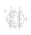
- Figure 1 provides a cross-sectional view of a Physics Package 102 for a CSAC 100 of one embodiment of the present invention.
- CSAC 100 comprises a vertical cavity surface emitting laser 110(vcsel) mounted and thermally coupled to a controllable heater block 111, a quarter wave plate (QWP)/ neutral density filter (IVDF) 120, a vapor cell 130 and a photo detector 140.
- QWP quarter wave plate
- IVDF neutral density filter
- another independent heater is provided around the vapor cell 130.
- the vcsel 110 and heater block 111 are supported within physics package 102 by a vcsel scaffold 150 comprising a silicon material.
- the quarter wave plate (QWP)/ neutral density filter (NDF) 120 is supported within physics package 102 by a QWP scaffold 160, also comprising a silicon material.
- a 4 ⁇ steradian iso-thermal cage (shown generally at 170) around vcsel 110 is formed when the QWP scaffold 160 is mounted in place onto the vcsel scaffold 150, as explained in greater detail below.
- An orifice 160 in the QWP scaffold provides an opening for the laser light 112 generated by vcsel 110 to exit the isothermal cage 170.
- there are layers of solder connecting all of the silicon components and connecting the various portions of the package (as described in United States Provisional Patent Application Serial No. 61/301,497 which is herein incorporated by reference).
- the temperature at the emitting surface of the vcsel 110 potentially could be several 10ths of a degree warmer than the base if black body radiation and trace gas thermal conduction were allowed to thermally couple vcsel 110 to the physics package 102. This is because when power is applied to the vcsel 110 die, the lasing surface at the top of the vcsel 110 die heats up, and that heat at the surface has to flow through the thermally-resistive body of vcsel 110 to reach the thermally-stabilized block 111 and package 102.
- iso-thermal cage 170 absent iso-thermal cage 170, if the outside walls of physics package 102 are exposed to cold exterior atmospheric conditions, black body radiation coupling would be established between vcsel 110 and physics package 102.
- Embodiments of the present invention make sure that the temperature of the iso-thermal cage 170 is at the same temperature as the base of heater block 111, which will be the same temperature as the base of vcsel 110.
- This configuration defeats black-body coupling between vcsel 110 and physics package 102, and trace gas thermal conduction, because such coupling cannot be established through the thermal barrier established by the heated iso-thermal cage 170.
- Figure 2 is a partially exploded cross-sectional diagram generally at 200 illustrating the formation of a 4 ⁇ steradian iso-thermal cage 270 formed from mounting a QWP scaffold 260 onto the vcsel scaffold 250.
- Vcsel scaffold 250 comprises a thermally resistive, structurally supportive, first support member 252 having a first surface 253 and a second surface 254, at least one silicon second support member 255 attached to the second surface 254, and a block of silicon material 256 6 attached to the second surface 254.
- the silicon material block 256 is approximately centered on first support member 252.
- the Vcsel scaffold 150 of Figure 1 comprises the structure illustrated by vcsel scaffold 250.
- the first surface 253 of first support member 252 supports a heater block 211 which is coupled to the base of vcsel 210.
- the a thermally resistive, structurally supportive, first support member 252 is made from polyimide.
- QWP scaffold 260 comprises a first support member 262 having a first surface 263 and a second surface 264 and at least one silicon second support member 265 attached to the second surface 264.
- QWP scaffold 260 further comprises silicon material attached to the second surface 264 of QWP scaffold 260 that define cage walls 272 and a cage ceiling 273 of the iso-thermal cage 270 formed when the QWP scaffold 260 is brought down from above and positioned on vcsel scaffold 250.
- An orifice 266 in the cage ceiling 273 an opening through first support member 262 for the laser light generated by vcsel 210 to exit the iso-thermal cage 270 (and in one embodiment, focus on a photo detector, such as shown in Figure 1 ).
- the cage walls 272 make contact with the vcsel scaffolding 250 above the silicon block 256, which functions the cage base of the iso-thermal cage 270.
- Silicon block 256 provides a thermally conductive path so that the cage walls 272 and ceiling 272 are thermally coupled to heater block 211 via the thermally conductive silicon material block 256, rather than being placed in direct contact with heater block 211.
- thermal energy produced by heater block 211 thus conductively provides heat to the base of vcsel 210 as well as the silicon base 256, walls 272 and ceiling 272 that form the iso-thermal cage 270 that surrounds vcsel 210.
- Figures 3A and 3B provides alternate embodiments for QWP scaffolding 260.
- figure 3A illustrates a silicon support member 364, cage walls 372, cage ceiling 373, orifice 360, and an inner thermal chamber 378 formed within silicon cage 270 that houses vcsel 210 and heater block 211.
- Figure 3B illustrates an alternate configuration with a silicon support member 364', cage walls 372', cage ceiling 373', orifice 360', and an inner thermal chamber 378' formed within silicon cage 270 that houses vcsel 210 and heater block 211.
- a consistent temperature is maintained at the vcsel (110, 210) by thermally isolating the vcsel within an iso-thermal cage (170, 270) thus preventing black-body radiation coupling between the vcsel, the physics package, or any other component within the CSAC.
- Figure 4 is a flow chart illustrating a method of one embodiment of the present invention.
- the method shown in Figure 4 provided for thermal isolation of a vertical cavity surface emitting laser (vcsel) assembly.
- vcsel vertical cavity surface emitting laser
- the method of Figure 4 provides for vcsel thermal stability by surrounding the surface of the vcsel with an isothermal cage.
- iso-thermal cage provided by embodiments of the present invention, radiative coupling and conductive coupling to components outside the iso-thermal cage are virtually eliminated, making it possible for the vcsel to remain thermally stable to within a fraction of a millidegree.
- the stability provided by the iso-thermal cages presented herein further provide for consistent operation the vcsel of a chip scale atomic clock at its desired operating point.
- the method begins a 410 with forming a first scaffold member from a first silicon wafer, the first scaffold member populated on a first side with a vertical cavity surface emitting laser (vcsel) and a heater block coupled to a base of the vcsel, the first scaffold member populated on a second side with a first silicon material block thermally coupled to the heater block through a first conductive path, the first silicon material block defining a base of an iso-thermal cage.
- vcsel vertical cavity surface emitting laser
- the method proceeds to 420 with forming a second scaffold member from a second silicon wafer, the second scaffold member populated with a second silicon material block having a thermal chamber therein defining at least one cage wall and a cage ceiling of the iso-thermal cage, the cage ceiling including an orifice.
- the method proceeds to 430 with aligning the second scaffold member and the first scaffold member such that the orifice provides an optical path for a laser light beam emitted from the vcsel.
- the method proceeds to 440 with coupling the second silicon material block to the first side of the first scaffold member such that a second conductive thermal path is formed between the at least one cage wall and the heater block via the first silicon material block.
- the vcsel is enclosed within the iso-thermal cage for 4 ⁇ steradians.
- the first scaffold member and the second scaffold will be secured within a physics package and the iso-thermal cage is positioned within the physics package to prevent black-body coupling between the vcsel and components external to the iso-thermal cage.
- the vcsel and the orifice are optically aligned within the physics package such that the laser light beam is focused on a photo detector.
- the physics package further includes a vapor cell external to the iso-thermal cage that defines at least part of the optical path for laser light between the vcsel and the photo detector.
Landscapes
- Physics & Mathematics (AREA)
- General Physics & Mathematics (AREA)
- Condensed Matter Physics & Semiconductors (AREA)
- Electromagnetism (AREA)
- Optics & Photonics (AREA)
- Semiconductor Lasers (AREA)
- Stabilization Of Oscillater, Synchronisation, Frequency Synthesizers (AREA)
Abstract
Description
- This application claims the benefit of United States Provisional Patent Application Serial No.
61/301,497, filed on February 4, 2010 - The U.S. Government may have certain rights in the present invention as provided for by the terms of a Government Contract prime number FA8650-O1-C-1125 with the U.S. Air Force.
- Chip Scale Atomic Clocks (CSACs) are not simply shrunken versions of bench-top atomic clocks. Several attributes that are unique to CSACs dominate their stability, their performance in the field, their reliability, and the economics associated with succeeding in a CSAC-based business. One of the more challenging aspects of making CSACs involves dealing with the temperature variations that various CSAC-based systems encounter during use. Conservatively, equipment with CSACs in the field can see temperatures ranging from -40°C to +65°C. In some environments temperatures approaching or even exceeding 100°C are frequently encountered - particularly for vehicle-mounted equipment. Even though every CSAC manufacturer attempts to stabilize the temperature of their most sensitive components, the temperature sensitivity of the CSACs can still be a problem. This is because radiative coupling and gas-phase thermal conduction from various components inside the CSAC's physics package to the walls of the package can cause the temperature of those components to change.
- In particular, the vcsel (vertical cavity surface emitting laser) in a CSAC is very sensitive to changes in temperature. For example, the base of the vcsel should be thermally stabilized to within a few thousandths of a degree to maintain precision operation. However, black-body radiation and thermal conduction through residual gas between the surface of the vcsel and the package walls can cause the upper light-emitting surface of the vcsel to change as ambient temperature changes. For example, as the ambient temperature changes from -40C to +65C, the surface of the vcsel could change by as much as 0.1C, even if the base of the vcsel is held at a stable temperature to within a fraction of a millidegree.
- For the reasons stated above and for other reasons stated below which will become apparent to those skilled in the art upon reading and understanding the specification, there is a need in the art for thermally stabilizing a vcsel in an atomic clock.
- The Embodiments of the present invention provide methods and systems for thermally stabilizing a vcsel in an atomic clock and will be understood by reading and studying the following specification.
- In one embodiment, a Chip-Scale Atomic Clock comprises: a vertical cavity surface emitting laser (vcsel); a heater block coupled to a base of the vcsel; a photo detector; a vapor cell, wherein the vapor cell includes a chamber that defines at least part of an optical path for laser light between the vcsel and the photo detector; and an iso-thermal cage surrounding the vcsel on all sides, the iso-thermal cage coupled to the heater block via a thermally conductive path.
- Embodiments of the present invention can be more easily understood and further advantages and uses thereof more readily apparent, when considered in view of the description of the preferred embodiments and the following figures in which:
-
Figure 1 is a diagram of a chip-scale atomic clock of one embodiment of the present invention; -
Figure 2 is a diagram of an iso-thermal cage of one embodiment of the present invention; -
Figures 3A and 3B are diagrams each illustrating cage walls and a cage ceiling for an isothermal cage of one embodiment of the present invention. -
Figure 4 is a flow chart illustrating a method of one embodiment of the present invention. - In accordance with common practice, the various described features are not drawn to scale but are drawn to emphasize features relevant to the present invention. Reference characters denote like elements throughout figures and text.
- In the following descriptions, reference is made to the accompanying drawings that form a part hereof, and in which is shown by way of specific illustrative embodiments in which the invention may be practiced. These embodiments are described in sufficient detail to enable those skilled in the art to practice the invention, and it is to be understood that other embodiments may be utilized and that logical, mechanical, electrical and method changes may be made without departing from the scope of the present invention. The following detailed description is, therefore, not to be taken in a limiting sense. Further, the various sections of this specification are not intended to be read in isolation but considered together with the teachings of the written description as a whole.
- Embodiments of the present invention address the problem of vcsel thermal stability by surrounding the vcsel through 4π Steradians (that is, on all sides) with an iso-thermal cage. As discussed below, embodiments of the present invention can be produced using standard MEMS processing steps that one of ordinary skill in the art upon reading this specification would recognizes as being compatible with mass production. By surrounding the surface of the vcsel with the isothermal cage, radiative coupling and conductive coupling to the outside world are virtually eliminated, making it possible for the vcsel to remain thermally stable to within a fraction of a millidegree as the ambient temperature varies from -40C to >65C.
-
Figure 1 provides a cross-sectional view of aPhysics Package 102 for aCSAC 100 of one embodiment of the present invention. CSAC 100 comprises a vertical cavity surface emitting laser 110(vcsel) mounted and thermally coupled to acontrollable heater block 111, a quarter wave plate (QWP)/ neutral density filter (IVDF) 120, avapor cell 130 and aphoto detector 140. In one embodiment of the present invention, anodic bonding is used during production ofvapor cell 130 to seal opticallyclear glass wafers 132 and 134 (for example, Pyrex or similar glass) to asilicon wafer substrate 136. At least onechamber 138 defined withinvapor cell 130 to provides an optical path (shown at 139) betweenvcsel 110 andphoto detector 140 forlaser light 112 transmitted byvcsel 110. In one embodiment, another independent heater is provided around thevapor cell 130. Thevcsel 110 andheater block 111 are supported withinphysics package 102 by avcsel scaffold 150 comprising a silicon material. The quarter wave plate (QWP)/ neutral density filter (NDF) 120 is supported withinphysics package 102 by aQWP scaffold 160, also comprising a silicon material. A 4π steradian iso-thermal cage (shown generally at 170) aroundvcsel 110 is formed when theQWP scaffold 160 is mounted in place onto thevcsel scaffold 150, as explained in greater detail below. Anorifice 160 in the QWP scaffold provides an opening for thelaser light 112 generated byvcsel 110 to exit theisothermal cage 170. Moreover, there are layers of solder connecting all of the silicon components and connecting the various portions of the package (as described in United States Provisional Patent Application Serial No.61/301,497 - Although temperature is regulated at the
heater block 111, the temperature at the emitting surface of thevcsel 110 potentially could be several 10ths of a degree warmer than the base if black body radiation and trace gas thermal conduction were allowed to thermally couplevcsel 110 to thephysics package 102. This is because when power is applied to thevcsel 110 die, the lasing surface at the top of thevcsel 110 die heats up, and that heat at the surface has to flow through the thermally-resistive body ofvcsel 110 to reach the thermally-stabilizedblock 111 andpackage 102. For example, absent iso-thermal cage 170, if the outside walls ofphysics package 102 are exposed to cold exterior atmospheric conditions, black body radiation coupling would be established betweenvcsel 110 andphysics package 102. Embodiments of the present invention make sure that the temperature of the iso-thermal cage 170 is at the same temperature as the base ofheater block 111, which will be the same temperature as the base ofvcsel 110. This configuration defeats black-body coupling betweenvcsel 110 andphysics package 102, and trace gas thermal conduction, because such coupling cannot be established through the thermal barrier established by the heated iso-thermal cage 170. This in turn ensures that there will be a fixed thermal offset between the lasing surface ofvcsel 110 and its thermally-stabilized base provides byblock 111, regardless of ambient temperatures. -
Figure 2 is a partially exploded cross-sectional diagram generally at 200 illustrating the formation of a 4π steradian iso-thermal cage 270 formed from mounting a QWP scaffold 260 onto thevcsel scaffold 250. -
Vcsel scaffold 250 comprises a thermally resistive, structurally supportive,first support member 252 having afirst surface 253 and asecond surface 254, at least one siliconsecond support member 255 attached to thesecond surface 254, and a block ofsilicon material 256 6 attached to thesecond surface 254. In the embodiment shown inFigure 2 , thesilicon material block 256 is approximately centered onfirst support member 252. In one embodiment, theVcsel scaffold 150 ofFigure 1 comprises the structure illustrated byvcsel scaffold 250. Thefirst surface 253 offirst support member 252 supports aheater block 211 which is coupled to the base ofvcsel 210. In one embodiment, the a thermally resistive, structurally supportive,first support member 252 is made from polyimide. - QWP scaffold 260 comprises a
first support member 262 having afirst surface 263 and asecond surface 264 and at least one siliconsecond support member 265 attached to thesecond surface 264. QWP scaffold 260 further comprises silicon material attached to thesecond surface 264 of QWP scaffold 260 that definecage walls 272 and acage ceiling 273 of the iso-thermal cage 270 formed when the QWP scaffold 260 is brought down from above and positioned onvcsel scaffold 250. Anorifice 266 in thecage ceiling 273 an opening throughfirst support member 262 for the laser light generated byvcsel 210 to exit the iso-thermal cage 270 (and in one embodiment, focus on a photo detector, such as shown inFigure 1 ). - As shown in
Figure 2 , thecage walls 272 make contact with thevcsel scaffolding 250 above thesilicon block 256, which functions the cage base of the iso-thermal cage 270.Silicon block 256 provides a thermally conductive path so that thecage walls 272 andceiling 272 are thermally coupled toheater block 211 via the thermally conductivesilicon material block 256, rather than being placed in direct contact withheater block 211. In operation, thermal energy produced byheater block 211 thus conductively provides heat to the base ofvcsel 210 as well as thesilicon base 256,walls 272 andceiling 272 that form the iso-thermal cage 270 that surroundsvcsel 210. -
Figures 3A and 3B provides alternate embodiments for QWP scaffolding 260. Looking down upon thesecond surface 264 of the QWP scaffolding 260,figure 3A illustrates asilicon support member 364,cage walls 372,cage ceiling 373,orifice 360, and an innerthermal chamber 378 formed withinsilicon cage 270 that housesvcsel 210 andheater block 211.Figure 3B illustrates an alternate configuration with a silicon support member 364', cage walls 372', cage ceiling 373', orifice 360', and an inner thermal chamber 378' formed withinsilicon cage 270 that houses vcsel 210 andheater block 211. - For the embodiments described in the
figures 1 ,2 and3A-3B and their descriptions above, a consistent temperature is maintained at the vcsel (110, 210) by thermally isolating the vcsel within an iso-thermal cage (170, 270) thus preventing black-body radiation coupling between the vcsel, the physics package, or any other component within the CSAC. -
Figure 4 is a flow chart illustrating a method of one embodiment of the present invention. In one embodiment, the method shown inFigure 4 provided for thermal isolation of a vertical cavity surface emitting laser (vcsel) assembly. One of ordinary skill in the art upon reading this specification would appreciate that standard MEMS processing techniques may be applied to perform the steps described inFigure 4 . The method ofFigure 4 provides for vcsel thermal stability by surrounding the surface of the vcsel with an isothermal cage. As previously explained, with the iso-thermal cage provided by embodiments of the present invention, radiative coupling and conductive coupling to components outside the iso-thermal cage are virtually eliminated, making it possible for the vcsel to remain thermally stable to within a fraction of a millidegree. The stability provided by the iso-thermal cages presented herein further provide for consistent operation the vcsel of a chip scale atomic clock at its desired operating point. - The method begins a 410 with forming a first scaffold member from a first silicon wafer, the first scaffold member populated on a first side with a vertical cavity surface emitting laser (vcsel) and a heater block coupled to a base of the vcsel, the first scaffold member populated on a second side with a first silicon material block thermally coupled to the heater block through a first conductive path, the first silicon material block defining a base of an iso-thermal cage.
- The method proceeds to 420 with forming a second scaffold member from a second silicon wafer, the second scaffold member populated with a second silicon material block having a thermal chamber therein defining at least one cage wall and a cage ceiling of the iso-thermal cage, the cage ceiling including an orifice.
- The method proceeds to 430 with aligning the second scaffold member and the first scaffold member such that the orifice provides an optical path for a laser light beam emitted from the vcsel.
- The method proceeds to 440 with coupling the second silicon material block to the first side of the first scaffold member such that a second conductive thermal path is formed between the at least one cage wall and the heater block via the first silicon material block. After coupling the second silicon material block to the first side of the first scaffold member, the vcsel is enclosed within the iso-thermal cage for 4π steradians.
- As illustrated previously in
Figure 2 , the first scaffold member and the second scaffold will be secured within a physics package and the iso-thermal cage is positioned within the physics package to prevent black-body coupling between the vcsel and components external to the iso-thermal cage. The vcsel and the orifice are optically aligned within the physics package such that the laser light beam is focused on a photo detector. In one embodiment, the physics package further includes a vapor cell external to the iso-thermal cage that defines at least part of the optical path for laser light between the vcsel and the photo detector. - Although the embodiments above generally describe embodiments of a vcsel utilized in the context of Chip-Scale Atomic Clocks, embodiments of the present invention are not only limited to Chip-Scale Atomic Clock applications. Other applications for vcsel are contemplated as within the scope of embodiments of the present invention. Further, although specific embodiments have been illustrated and described herein, it will be appreciated by those of ordinary skill in the art that any arrangement, which is calculated to achieve the same purpose, may be substituted for the specific embodiment shown. This application is intended to cover any adaptations or variations of the present invention. Therefore, it is manifestly intended that this invention be limited only by the claims and the equivalents thereof.
Claims (10)
- A vertical cavity surface emitting laser (vcsel) assembly, the assembly comprising:a vertical cavity surface emitting laser (vcsel) 110;a heater block 111 coupled to a base of the vcsel 110; andan iso-thermal cage 170 surrounding the vcsel 110 on all sides, the iso-thermal cage 170 coupled to the heater block 111 via a thermally conductive path.
- The assembly of claim 1, the iso-thermal cage 170 further comprising an orifice 266 aligned with the vcsel 110, the orifice 266 providing an optical path out of the iso-thermal cage 170 for laser light 112 emitted from the vcsel 110.
- The assembly of claim 1, the iso-thermal cage 170 further comprising a cage base 256, at least one cage wall 272 and a cage ceiling 273;
wherein the at least one cage wall 272 and cage ceiling 273 are thermally coupled via a conductive path through the cage base 256 to the heater block 111. - The assembly of claim 1, further comprising:a first scaffold member 250 configured to support the vcsel 110, 210 and the heater block 111, 211 within a physic package 102, the first scaffold member 250 comprising a first support member 252;wherein the first support member 252 includes a first surface 253 coupled to the heater block 111, 211 and a second surface 254 coupled to the cage base 256, the cage base 256 thermally coupled to the heater block 111 via a conductive path through the first support member 252.
- The assembly of claim 1, wherein the first support member 252 and the cage base 256 are formed from a first silicon wafer, and the least one cage wall 272 and cage ceiling 273 are formed from a second silicon wafer.
- A method for providing thermal isolation of a vertical cavity surface emitting laser (vcsel 110) assembly, the method comprising:forming a first scaffold member 250 from a first silicon wafer, the first scaffold member populated on a first side 253 with a vertical cavity surface emitting laser (vcsel) 210 and a heater block 211 coupled to a base of the vcsel 210, the first scaffold member 250 populated on a second side 254 with a first silicon material block 256 thermally coupled to the heater block 111 I through a first conductive path, the first silicon material block 256 defining a base of an isothermal cage 270;forming a second scaffold member 260 from a second silicon wafer, the second scaffold 260 member populated with a second silicon material block 272, 273 having a thermal chamber therein defining at least one cage wall 272 and a cage ceiling 273 of the iso-thermal cage 270, the cage ceiling 273 including an orifice 266;aligning the second scaffold member 260 and the first scaffold member 250 such that the orifice 266 provides an optical path for a laser light 112 beam emitted from the vcsel 210; andcoupling the second silicon material block 272, 273 to the first side of the first scaffold member s250 uch that a second conductive thermal path is formed between the at least one cage wall 272 and the heater block 111 via the first silicon material block 272,273;wherein after coupling the second silicon material block 272, 273 to the first side of the first scaffold member 250, the vcsel 210 is enclosed within the iso-thermal cage 270 on all sides.
- The method of claim 6, further comprising:securing the first scaffold member 250 and the second scaffold member 260 within a physics package 102.
- The method of claim 7, wherein the iso-thermal cage 170 is positioned within the physics package 102 to prevent black-body coupling between the vcsel 210 and components external to the iso-thermal cage 270.
- The method of claim 7, wherein the vcsel 210 and the orifice 266 are optically aligned within the physics package 102 such that the laser light 112 beam is focused on a photo detector 140.
- The method of claim 9, wherein the physics package 102 further includes a vapor cell 130 external to the iso-thermal cage 170 that defines at least part of the optical path for laser light 112 between the vcsel 110 and the photo detector 140.
Applications Claiming Priority (2)
| Application Number | Priority Date | Filing Date | Title |
|---|---|---|---|
| US30149710P | 2010-02-04 | 2010-02-04 | |
| US12/884,489 US8218590B2 (en) | 2010-02-04 | 2010-09-17 | Designs and processes for thermally stabilizing a vertical cavity surface emitting laser (vcsel) in a chip-scale atomic clock |
Publications (3)
| Publication Number | Publication Date |
|---|---|
| EP2355271A2 true EP2355271A2 (en) | 2011-08-10 |
| EP2355271A3 EP2355271A3 (en) | 2017-03-15 |
| EP2355271B1 EP2355271B1 (en) | 2020-08-19 |
Family
ID=43769119
Family Applications (1)
| Application Number | Title | Priority Date | Filing Date |
|---|---|---|---|
| EP10189741.1A Active EP2355271B1 (en) | 2010-02-04 | 2010-11-02 | Designs and processes for thermally stabilizing a vertical cavity surface emitting laser (vcsel) in a chip-scale atomic clock |
Country Status (4)
| Country | Link |
|---|---|
| US (1) | US8218590B2 (en) |
| EP (1) | EP2355271B1 (en) |
| JP (1) | JP5785380B2 (en) |
| IL (1) | IL209174A (en) |
Cited By (2)
| Publication number | Priority date | Publication date | Assignee | Title |
|---|---|---|---|---|
| CN104734008A (en) * | 2013-12-20 | 2015-06-24 | 精工爱普生株式会社 | Vertical cavity surface emitting laser and atomic oscillator |
| CN105137741A (en) * | 2015-10-21 | 2015-12-09 | 成都天奥电子股份有限公司 | Vibration-proof CSAC (chip-scale atomic clock) physical system |
Families Citing this family (13)
| Publication number | Priority date | Publication date | Assignee | Title |
|---|---|---|---|---|
| US8299860B2 (en) | 2010-02-04 | 2012-10-30 | Honeywell International Inc. | Fabrication techniques to enhance pressure uniformity in anodically bonded vapor cells |
| US8941442B2 (en) | 2010-02-04 | 2015-01-27 | Honeywell International Inc. | Fabrication techniques to enhance pressure uniformity in anodically bonded vapor cells |
| US8624682B2 (en) | 2011-06-13 | 2014-01-07 | Honeywell International Inc. | Vapor cell atomic clock physics package |
| US8837540B2 (en) | 2011-06-29 | 2014-09-16 | Honeywell International Inc. | Simple, low power microsystem for saturation spectroscopy |
| US20130341502A1 (en) * | 2012-06-22 | 2013-12-26 | Alan Cowie | Method and apparatus for two point calibration of a tunable diode laser analyzer |
| JP6119294B2 (en) * | 2013-02-18 | 2017-04-26 | セイコーエプソン株式会社 | Quantum interference device, atomic oscillator, and moving object |
| JP2015119149A (en) * | 2013-12-20 | 2015-06-25 | セイコーエプソン株式会社 | Surface emitting laser and atomic oscillator |
| JP2015119143A (en) * | 2013-12-20 | 2015-06-25 | セイコーエプソン株式会社 | Surface emitting laser and atomic oscillator |
| JP6264876B2 (en) * | 2013-12-20 | 2018-01-24 | セイコーエプソン株式会社 | Quantum interference devices, atomic oscillators, and electronic equipment |
| JP2016207695A (en) | 2015-04-15 | 2016-12-08 | セイコーエプソン株式会社 | Atomic cell, method for manufacturing atomic cell, quantum interference device, atomic oscillator, electronic apparatus and mobile body |
| JP2017183377A (en) | 2016-03-29 | 2017-10-05 | セイコーエプソン株式会社 | Quantum interference device, atomic oscillator, electronic apparatus and mobile |
| US10749539B2 (en) | 2018-03-26 | 2020-08-18 | Honeywell International Inc. | Apparatus and method for a vapor cell atomic frequency reference |
| JP7780803B2 (en) * | 2020-11-06 | 2025-12-05 | 国立大学法人京都大学 | Metal gas filled cell and its manufacturing method |
Family Cites Families (12)
| Publication number | Priority date | Publication date | Assignee | Title |
|---|---|---|---|---|
| JPS58114061U (en) * | 1982-01-29 | 1983-08-04 | キヤノン株式会社 | light beam generator |
| JPH06203403A (en) * | 1992-10-22 | 1994-07-22 | Matsushita Electron Corp | Semiconductor laser device and optical pickup device |
| US6172570B1 (en) * | 1999-08-23 | 2001-01-09 | Datum, Inc. | Laser light quantum system |
| JP4192517B2 (en) * | 2002-07-18 | 2008-12-10 | ソニー株式会社 | Optical semiconductor device and manufacturing method thereof |
| US7356057B2 (en) | 2002-10-31 | 2008-04-08 | Finisar Corporation | Wide temperature range vertical cavity surface emitting laser |
| US7075962B2 (en) | 2003-06-27 | 2006-07-11 | Finisar Corporation | VCSEL having thermal management |
| US7292111B2 (en) * | 2004-04-26 | 2007-11-06 | Northrop Grumman Corporation | Middle layer of die structure that comprises a cavity that holds an alkali metal |
| US20060022213A1 (en) * | 2004-08-02 | 2006-02-02 | Posamentier Joshua D | TO-can heater on flex circuit |
| US7750356B2 (en) * | 2005-05-04 | 2010-07-06 | Avago Technologies Fiber Ip (Singapore) Pte. Ltd. | Silicon optical package with 45 degree turning mirror |
| JP5228275B2 (en) * | 2005-12-28 | 2013-07-03 | セイコーエプソン株式会社 | Atomic frequency acquisition device and atomic clock |
| JP5375279B2 (en) * | 2008-06-18 | 2013-12-25 | セイコーエプソン株式会社 | Atomic oscillator |
| US8067991B2 (en) * | 2010-02-04 | 2011-11-29 | Honeywell International Inc. | Chip-scale atomic clock with two thermal zones |
-
2010
- 2010-09-17 US US12/884,489 patent/US8218590B2/en active Active
- 2010-11-02 EP EP10189741.1A patent/EP2355271B1/en active Active
- 2010-11-07 IL IL209174A patent/IL209174A/en not_active IP Right Cessation
- 2010-11-09 JP JP2010250738A patent/JP5785380B2/en active Active
Cited By (3)
| Publication number | Priority date | Publication date | Assignee | Title |
|---|---|---|---|---|
| CN104734008A (en) * | 2013-12-20 | 2015-06-24 | 精工爱普生株式会社 | Vertical cavity surface emitting laser and atomic oscillator |
| CN104734008B (en) * | 2013-12-20 | 2019-07-26 | 精工爱普生株式会社 | Surface-emitting lasers and atomic oscillators |
| CN105137741A (en) * | 2015-10-21 | 2015-12-09 | 成都天奥电子股份有限公司 | Vibration-proof CSAC (chip-scale atomic clock) physical system |
Also Published As
| Publication number | Publication date |
|---|---|
| US8218590B2 (en) | 2012-07-10 |
| IL209174A (en) | 2015-05-31 |
| US20110188524A1 (en) | 2011-08-04 |
| EP2355271A3 (en) | 2017-03-15 |
| EP2355271B1 (en) | 2020-08-19 |
| IL209174A0 (en) | 2011-04-28 |
| JP5785380B2 (en) | 2015-09-30 |
| JP2011238893A (en) | 2011-11-24 |
Similar Documents
| Publication | Publication Date | Title |
|---|---|---|
| US8218590B2 (en) | Designs and processes for thermally stabilizing a vertical cavity surface emitting laser (vcsel) in a chip-scale atomic clock | |
| JP5616752B2 (en) | Chip-scale atomic clock with two thermal zones | |
| US7215213B2 (en) | Apparatus and system for suspending a chip-scale device and related methods | |
| US10566363B2 (en) | Light emitter and light detector modules including vertical alignment features | |
| TWI885832B (en) | Light detection device | |
| US20180313913A1 (en) | Physics Package for Compact Atomic Device | |
| US6900702B2 (en) | MEMS frequency standard for devices such as atomic clock | |
| EP1591846B1 (en) | Middle layer of die structure that comprises a cavity that holds an alkali metal | |
| EP1816454A1 (en) | Infrared sensor | |
| US20060022213A1 (en) | TO-can heater on flex circuit | |
| Mescher et al. | An ultra-low-power physics package for a chip-scale atomic clock | |
| CN104880780A (en) | Optical Module And Light Transmission Method | |
| JP2015165556A (en) | Atomic source with heater on thermal isolation die | |
| KR101709557B1 (en) | Vapor cell with electro-optical function for chip-scale atomic clock | |
| JP2010151639A (en) | Thermopile infrared detector | |
| CN101213429B (en) | Device for detecting electromagnetic wave and method for producing the same | |
| Gruet et al. | A miniature frequency-stabilized VCSEL system emitting at 795 nm based on LTCC modules | |
| CN116482813A (en) | Compact Micro-Platform for Optical Transceiver Assemblies | |
| Karioja et al. | MEMS, MOEMS, RF-MEMS and photonics packaging based on LTCC technology | |
| US20050232545A1 (en) | Active optical alignment and attachment thereto of a semiconductor optical component with an optical element formed on a planar lightwave circuit | |
| US20220334004A1 (en) | Fiber Optic Temperature Sensor Having Encapsulated Sensing Element | |
| KR102045105B1 (en) | Methods of attaching a module on wafer substrate | |
| Biermann et al. | Advanced broadband MEMS infrared emitter based on high-temperature-resistant nanostructured surfaces and packaging solutions for harsh environments | |
| JP2020113616A (en) | Quantum optics | |
| US20180364439A1 (en) | Wafer level integrated optics in packaging for imaging sensor application |
Legal Events
| Date | Code | Title | Description |
|---|---|---|---|
| PUAI | Public reference made under article 153(3) epc to a published international application that has entered the european phase |
Free format text: ORIGINAL CODE: 0009012 |
|
| 17P | Request for examination filed |
Effective date: 20101102 |
|
| AK | Designated contracting states |
Kind code of ref document: A2 Designated state(s): AL AT BE BG CH CY CZ DE DK EE ES FI FR GB GR HR HU IE IS IT LI LT LU LV MC MK MT NL NO PL PT RO RS SE SI SK SM TR |
|
| AX | Request for extension of the european patent |
Extension state: BA ME |
|
| RAP1 | Party data changed (applicant data changed or rights of an application transferred) |
Owner name: HONEYWELL INTERNATIONAL INC. |
|
| PUAL | Search report despatched |
Free format text: ORIGINAL CODE: 0009013 |
|
| STAA | Information on the status of an ep patent application or granted ep patent |
Free format text: STATUS: EXAMINATION IS IN PROGRESS |
|
| AK | Designated contracting states |
Kind code of ref document: A3 Designated state(s): AL AT BE BG CH CY CZ DE DK EE ES FI FR GB GR HR HU IE IS IT LI LT LU LV MC MK MT NL NO PL PT RO RS SE SI SK SM TR |
|
| AX | Request for extension of the european patent |
Extension state: BA ME |
|
| RIC1 | Information provided on ipc code assigned before grant |
Ipc: H01S 5/183 20060101ALI20170208BHEP Ipc: H01S 5/02 20060101ALN20170208BHEP Ipc: H01S 5/024 20060101AFI20170208BHEP Ipc: H01S 5/022 20060101ALN20170208BHEP Ipc: G04F 5/14 20060101ALI20170208BHEP Ipc: H01S 5/00 20060101ALN20170208BHEP |
|
| 17Q | First examination report despatched |
Effective date: 20170308 |
|
| REG | Reference to a national code |
Ref country code: DE Ref legal event code: R079 Ref document number: 602010065204 Country of ref document: DE Free format text: PREVIOUS MAIN CLASS: H01S0005022000 Ipc: H01S0005024000 |
|
| GRAP | Despatch of communication of intention to grant a patent |
Free format text: ORIGINAL CODE: EPIDOSNIGR1 |
|
| STAA | Information on the status of an ep patent application or granted ep patent |
Free format text: STATUS: GRANT OF PATENT IS INTENDED |
|
| RIC1 | Information provided on ipc code assigned before grant |
Ipc: H01S 5/022 20060101ALI20200402BHEP Ipc: H01S 5/024 20060101AFI20200402BHEP Ipc: G04F 5/14 20060101ALI20200402BHEP Ipc: H01S 5/183 20060101ALI20200402BHEP Ipc: H01S 5/00 20060101ALN20200402BHEP Ipc: H01S 5/02 20060101ALN20200402BHEP |
|
| INTG | Intention to grant announced |
Effective date: 20200417 |
|
| RIN1 | Information on inventor provided before grant (corrected) |
Inventor name: RIDLEY, JEFF A. Inventor name: LU, SON T. Inventor name: FORNER, LINDA J. Inventor name: YOUNGNER, DANIEL W. |
|
| GRAS | Grant fee paid |
Free format text: ORIGINAL CODE: EPIDOSNIGR3 |
|
| GRAA | (expected) grant |
Free format text: ORIGINAL CODE: 0009210 |
|
| STAA | Information on the status of an ep patent application or granted ep patent |
Free format text: STATUS: THE PATENT HAS BEEN GRANTED |
|
| AK | Designated contracting states |
Kind code of ref document: B1 Designated state(s): AL AT BE BG CH CY CZ DE DK EE ES FI FR GB GR HR HU IE IS IT LI LT LU LV MC MK MT NL NO PL PT RO RS SE SI SK SM TR |
|
| REG | Reference to a national code |
Ref country code: GB Ref legal event code: FG4D |
|
| REG | Reference to a national code |
Ref country code: CH Ref legal event code: EP |
|
| REG | Reference to a national code |
Ref country code: DE Ref legal event code: R096 Ref document number: 602010065204 Country of ref document: DE |
|
| REG | Reference to a national code |
Ref country code: AT Ref legal event code: REF Ref document number: 1305034 Country of ref document: AT Kind code of ref document: T Effective date: 20200915 |
|
| REG | Reference to a national code |
Ref country code: IE Ref legal event code: FG4D |
|
| REG | Reference to a national code |
Ref country code: LT Ref legal event code: MG4D |
|
| REG | Reference to a national code |
Ref country code: NL Ref legal event code: MP Effective date: 20200819 |
|
| PG25 | Lapsed in a contracting state [announced via postgrant information from national office to epo] |
Ref country code: PT Free format text: LAPSE BECAUSE OF FAILURE TO SUBMIT A TRANSLATION OF THE DESCRIPTION OR TO PAY THE FEE WITHIN THE PRESCRIBED TIME-LIMIT Effective date: 20201221 Ref country code: LT Free format text: LAPSE BECAUSE OF FAILURE TO SUBMIT A TRANSLATION OF THE DESCRIPTION OR TO PAY THE FEE WITHIN THE PRESCRIBED TIME-LIMIT Effective date: 20200819 Ref country code: HR Free format text: LAPSE BECAUSE OF FAILURE TO SUBMIT A TRANSLATION OF THE DESCRIPTION OR TO PAY THE FEE WITHIN THE PRESCRIBED TIME-LIMIT Effective date: 20200819 Ref country code: SE Free format text: LAPSE BECAUSE OF FAILURE TO SUBMIT A TRANSLATION OF THE DESCRIPTION OR TO PAY THE FEE WITHIN THE PRESCRIBED TIME-LIMIT Effective date: 20200819 Ref country code: NO Free format text: LAPSE BECAUSE OF FAILURE TO SUBMIT A TRANSLATION OF THE DESCRIPTION OR TO PAY THE FEE WITHIN THE PRESCRIBED TIME-LIMIT Effective date: 20201119 Ref country code: FI Free format text: LAPSE BECAUSE OF FAILURE TO SUBMIT A TRANSLATION OF THE DESCRIPTION OR TO PAY THE FEE WITHIN THE PRESCRIBED TIME-LIMIT Effective date: 20200819 Ref country code: BG Free format text: LAPSE BECAUSE OF FAILURE TO SUBMIT A TRANSLATION OF THE DESCRIPTION OR TO PAY THE FEE WITHIN THE PRESCRIBED TIME-LIMIT Effective date: 20201119 Ref country code: GR Free format text: LAPSE BECAUSE OF FAILURE TO SUBMIT A TRANSLATION OF THE DESCRIPTION OR TO PAY THE FEE WITHIN THE PRESCRIBED TIME-LIMIT Effective date: 20201120 |
|
| REG | Reference to a national code |
Ref country code: AT Ref legal event code: MK05 Ref document number: 1305034 Country of ref document: AT Kind code of ref document: T Effective date: 20200819 |
|
| PG25 | Lapsed in a contracting state [announced via postgrant information from national office to epo] |
Ref country code: RS Free format text: LAPSE BECAUSE OF FAILURE TO SUBMIT A TRANSLATION OF THE DESCRIPTION OR TO PAY THE FEE WITHIN THE PRESCRIBED TIME-LIMIT Effective date: 20200819 Ref country code: PL Free format text: LAPSE BECAUSE OF FAILURE TO SUBMIT A TRANSLATION OF THE DESCRIPTION OR TO PAY THE FEE WITHIN THE PRESCRIBED TIME-LIMIT Effective date: 20200819 Ref country code: NL Free format text: LAPSE BECAUSE OF FAILURE TO SUBMIT A TRANSLATION OF THE DESCRIPTION OR TO PAY THE FEE WITHIN THE PRESCRIBED TIME-LIMIT Effective date: 20200819 Ref country code: LV Free format text: LAPSE BECAUSE OF FAILURE TO SUBMIT A TRANSLATION OF THE DESCRIPTION OR TO PAY THE FEE WITHIN THE PRESCRIBED TIME-LIMIT Effective date: 20200819 Ref country code: IS Free format text: LAPSE BECAUSE OF FAILURE TO SUBMIT A TRANSLATION OF THE DESCRIPTION OR TO PAY THE FEE WITHIN THE PRESCRIBED TIME-LIMIT Effective date: 20201219 |
|
| PG25 | Lapsed in a contracting state [announced via postgrant information from national office to epo] |
Ref country code: DK Free format text: LAPSE BECAUSE OF FAILURE TO SUBMIT A TRANSLATION OF THE DESCRIPTION OR TO PAY THE FEE WITHIN THE PRESCRIBED TIME-LIMIT Effective date: 20200819 Ref country code: CZ Free format text: LAPSE BECAUSE OF FAILURE TO SUBMIT A TRANSLATION OF THE DESCRIPTION OR TO PAY THE FEE WITHIN THE PRESCRIBED TIME-LIMIT Effective date: 20200819 Ref country code: EE Free format text: LAPSE BECAUSE OF FAILURE TO SUBMIT A TRANSLATION OF THE DESCRIPTION OR TO PAY THE FEE WITHIN THE PRESCRIBED TIME-LIMIT Effective date: 20200819 Ref country code: RO Free format text: LAPSE BECAUSE OF FAILURE TO SUBMIT A TRANSLATION OF THE DESCRIPTION OR TO PAY THE FEE WITHIN THE PRESCRIBED TIME-LIMIT Effective date: 20200819 Ref country code: SM Free format text: LAPSE BECAUSE OF FAILURE TO SUBMIT A TRANSLATION OF THE DESCRIPTION OR TO PAY THE FEE WITHIN THE PRESCRIBED TIME-LIMIT Effective date: 20200819 |
|
| REG | Reference to a national code |
Ref country code: DE Ref legal event code: R097 Ref document number: 602010065204 Country of ref document: DE |
|
| PG25 | Lapsed in a contracting state [announced via postgrant information from national office to epo] |
Ref country code: ES Free format text: LAPSE BECAUSE OF FAILURE TO SUBMIT A TRANSLATION OF THE DESCRIPTION OR TO PAY THE FEE WITHIN THE PRESCRIBED TIME-LIMIT Effective date: 20200819 Ref country code: AT Free format text: LAPSE BECAUSE OF FAILURE TO SUBMIT A TRANSLATION OF THE DESCRIPTION OR TO PAY THE FEE WITHIN THE PRESCRIBED TIME-LIMIT Effective date: 20200819 Ref country code: AL Free format text: LAPSE BECAUSE OF FAILURE TO SUBMIT A TRANSLATION OF THE DESCRIPTION OR TO PAY THE FEE WITHIN THE PRESCRIBED TIME-LIMIT Effective date: 20200819 |
|
| REG | Reference to a national code |
Ref country code: DE Ref legal event code: R119 Ref document number: 602010065204 Country of ref document: DE |
|
| PLBE | No opposition filed within time limit |
Free format text: ORIGINAL CODE: 0009261 |
|
| STAA | Information on the status of an ep patent application or granted ep patent |
Free format text: STATUS: NO OPPOSITION FILED WITHIN TIME LIMIT |
|
| PG25 | Lapsed in a contracting state [announced via postgrant information from national office to epo] |
Ref country code: MC Free format text: LAPSE BECAUSE OF FAILURE TO SUBMIT A TRANSLATION OF THE DESCRIPTION OR TO PAY THE FEE WITHIN THE PRESCRIBED TIME-LIMIT Effective date: 20200819 Ref country code: SK Free format text: LAPSE BECAUSE OF FAILURE TO SUBMIT A TRANSLATION OF THE DESCRIPTION OR TO PAY THE FEE WITHIN THE PRESCRIBED TIME-LIMIT Effective date: 20200819 |
|
| REG | Reference to a national code |
Ref country code: CH Ref legal event code: PL |
|
| 26N | No opposition filed |
Effective date: 20210520 |
|
| GBPC | Gb: european patent ceased through non-payment of renewal fee |
Effective date: 20201119 |
|
| PG25 | Lapsed in a contracting state [announced via postgrant information from national office to epo] |
Ref country code: IT Free format text: LAPSE BECAUSE OF FAILURE TO SUBMIT A TRANSLATION OF THE DESCRIPTION OR TO PAY THE FEE WITHIN THE PRESCRIBED TIME-LIMIT Effective date: 20200819 Ref country code: LU Free format text: LAPSE BECAUSE OF NON-PAYMENT OF DUE FEES Effective date: 20201102 |
|
| REG | Reference to a national code |
Ref country code: BE Ref legal event code: MM Effective date: 20201130 |
|
| PG25 | Lapsed in a contracting state [announced via postgrant information from national office to epo] |
Ref country code: LI Free format text: LAPSE BECAUSE OF NON-PAYMENT OF DUE FEES Effective date: 20201130 Ref country code: SI Free format text: LAPSE BECAUSE OF FAILURE TO SUBMIT A TRANSLATION OF THE DESCRIPTION OR TO PAY THE FEE WITHIN THE PRESCRIBED TIME-LIMIT Effective date: 20200819 Ref country code: CH Free format text: LAPSE BECAUSE OF NON-PAYMENT OF DUE FEES Effective date: 20201130 |
|
| PG25 | Lapsed in a contracting state [announced via postgrant information from national office to epo] |
Ref country code: IE Free format text: LAPSE BECAUSE OF NON-PAYMENT OF DUE FEES Effective date: 20201102 |
|
| PG25 | Lapsed in a contracting state [announced via postgrant information from national office to epo] |
Ref country code: GB Free format text: LAPSE BECAUSE OF NON-PAYMENT OF DUE FEES Effective date: 20201119 Ref country code: DE Free format text: LAPSE BECAUSE OF NON-PAYMENT OF DUE FEES Effective date: 20210601 |
|
| PG25 | Lapsed in a contracting state [announced via postgrant information from national office to epo] |
Ref country code: IS Free format text: LAPSE BECAUSE OF FAILURE TO SUBMIT A TRANSLATION OF THE DESCRIPTION OR TO PAY THE FEE WITHIN THE PRESCRIBED TIME-LIMIT Effective date: 20201219 Ref country code: TR Free format text: LAPSE BECAUSE OF FAILURE TO SUBMIT A TRANSLATION OF THE DESCRIPTION OR TO PAY THE FEE WITHIN THE PRESCRIBED TIME-LIMIT Effective date: 20200819 Ref country code: MT Free format text: LAPSE BECAUSE OF FAILURE TO SUBMIT A TRANSLATION OF THE DESCRIPTION OR TO PAY THE FEE WITHIN THE PRESCRIBED TIME-LIMIT Effective date: 20200819 Ref country code: CY Free format text: LAPSE BECAUSE OF FAILURE TO SUBMIT A TRANSLATION OF THE DESCRIPTION OR TO PAY THE FEE WITHIN THE PRESCRIBED TIME-LIMIT Effective date: 20200819 |
|
| PG25 | Lapsed in a contracting state [announced via postgrant information from national office to epo] |
Ref country code: MK Free format text: LAPSE BECAUSE OF FAILURE TO SUBMIT A TRANSLATION OF THE DESCRIPTION OR TO PAY THE FEE WITHIN THE PRESCRIBED TIME-LIMIT Effective date: 20200819 |
|
| PG25 | Lapsed in a contracting state [announced via postgrant information from national office to epo] |
Ref country code: BE Free format text: LAPSE BECAUSE OF NON-PAYMENT OF DUE FEES Effective date: 20201130 |
|
| P01 | Opt-out of the competence of the unified patent court (upc) registered |
Effective date: 20230525 |
|
| PGFP | Annual fee paid to national office [announced via postgrant information from national office to epo] |
Ref country code: FR Payment date: 20251125 Year of fee payment: 16 |