EP2355184A2 - Light emitting device, light emitting device package, and lighting system - Google Patents
Light emitting device, light emitting device package, and lighting system Download PDFInfo
- Publication number
- EP2355184A2 EP2355184A2 EP11152802A EP11152802A EP2355184A2 EP 2355184 A2 EP2355184 A2 EP 2355184A2 EP 11152802 A EP11152802 A EP 11152802A EP 11152802 A EP11152802 A EP 11152802A EP 2355184 A2 EP2355184 A2 EP 2355184A2
- Authority
- EP
- European Patent Office
- Prior art keywords
- light emitting
- semiconductor layer
- emitting device
- face
- protrusions
- Prior art date
- Legal status (The legal status is an assumption and is not a legal conclusion. Google has not performed a legal analysis and makes no representation as to the accuracy of the status listed.)
- Granted
Links
Images


Classifications
-
- H—ELECTRICITY
- H10—SEMICONDUCTOR DEVICES; ELECTRIC SOLID-STATE DEVICES NOT OTHERWISE PROVIDED FOR
- H10H—INORGANIC LIGHT-EMITTING SEMICONDUCTOR DEVICES HAVING POTENTIAL BARRIERS
- H10H20/00—Individual inorganic light-emitting semiconductor devices having potential barriers, e.g. light-emitting diodes [LED]
- H10H20/80—Constructional details
- H10H20/81—Bodies
- H10H20/819—Bodies characterised by their shape, e.g. curved or truncated substrates
- H10H20/82—Roughened surfaces, e.g. at the interface between epitaxial layers
-
- H—ELECTRICITY
- H10—SEMICONDUCTOR DEVICES; ELECTRIC SOLID-STATE DEVICES NOT OTHERWISE PROVIDED FOR
- H10H—INORGANIC LIGHT-EMITTING SEMICONDUCTOR DEVICES HAVING POTENTIAL BARRIERS
- H10H20/00—Individual inorganic light-emitting semiconductor devices having potential barriers, e.g. light-emitting diodes [LED]
- H10H20/80—Constructional details
- H10H20/81—Bodies
- H10H20/817—Bodies characterised by the crystal structures or orientations, e.g. polycrystalline, amorphous or porous
-
- H—ELECTRICITY
- H10—SEMICONDUCTOR DEVICES; ELECTRIC SOLID-STATE DEVICES NOT OTHERWISE PROVIDED FOR
- H10H—INORGANIC LIGHT-EMITTING SEMICONDUCTOR DEVICES HAVING POTENTIAL BARRIERS
- H10H20/00—Individual inorganic light-emitting semiconductor devices having potential barriers, e.g. light-emitting diodes [LED]
- H10H20/80—Constructional details
- H10H20/81—Bodies
- H10H20/819—Bodies characterised by their shape, e.g. curved or truncated substrates
-
- H—ELECTRICITY
- H10—SEMICONDUCTOR DEVICES; ELECTRIC SOLID-STATE DEVICES NOT OTHERWISE PROVIDED FOR
- H10H—INORGANIC LIGHT-EMITTING SEMICONDUCTOR DEVICES HAVING POTENTIAL BARRIERS
- H10H20/00—Individual inorganic light-emitting semiconductor devices having potential barriers, e.g. light-emitting diodes [LED]
- H10H20/01—Manufacture or treatment
- H10H20/011—Manufacture or treatment of bodies, e.g. forming semiconductor layers
- H10H20/013—Manufacture or treatment of bodies, e.g. forming semiconductor layers having light-emitting regions comprising only Group III-V materials
- H10H20/0133—Manufacture or treatment of bodies, e.g. forming semiconductor layers having light-emitting regions comprising only Group III-V materials with a substrate not being Group III-V materials
- H10H20/01335—Manufacture or treatment of bodies, e.g. forming semiconductor layers having light-emitting regions comprising only Group III-V materials with a substrate not being Group III-V materials the light-emitting regions comprising nitride materials
-
- H—ELECTRICITY
- H10—SEMICONDUCTOR DEVICES; ELECTRIC SOLID-STATE DEVICES NOT OTHERWISE PROVIDED FOR
- H10H—INORGANIC LIGHT-EMITTING SEMICONDUCTOR DEVICES HAVING POTENTIAL BARRIERS
- H10H20/00—Individual inorganic light-emitting semiconductor devices having potential barriers, e.g. light-emitting diodes [LED]
- H10H20/80—Constructional details
- H10H20/81—Bodies
- H10H20/822—Materials of the light-emitting regions
- H10H20/824—Materials of the light-emitting regions comprising only Group III-V materials, e.g. GaP
- H10H20/825—Materials of the light-emitting regions comprising only Group III-V materials, e.g. GaP containing nitrogen, e.g. GaN
-
- H—ELECTRICITY
- H10—SEMICONDUCTOR DEVICES; ELECTRIC SOLID-STATE DEVICES NOT OTHERWISE PROVIDED FOR
- H10W—GENERIC PACKAGES, INTERCONNECTIONS, CONNECTORS OR OTHER CONSTRUCTIONAL DETAILS OF DEVICES COVERED BY CLASS H10
- H10W72/00—Interconnections or connectors in packages
- H10W72/071—Connecting or disconnecting
- H10W72/075—Connecting or disconnecting of bond wires
- H10W72/07551—Connecting or disconnecting of bond wires characterised by changes in properties of the bond wires during the connecting
- H10W72/07554—Connecting or disconnecting of bond wires characterised by changes in properties of the bond wires during the connecting changes in dispositions
-
- H—ELECTRICITY
- H10—SEMICONDUCTOR DEVICES; ELECTRIC SOLID-STATE DEVICES NOT OTHERWISE PROVIDED FOR
- H10W—GENERIC PACKAGES, INTERCONNECTIONS, CONNECTORS OR OTHER CONSTRUCTIONAL DETAILS OF DEVICES COVERED BY CLASS H10
- H10W72/00—Interconnections or connectors in packages
- H10W72/50—Bond wires
- H10W72/541—Dispositions of bond wires
- H10W72/547—Dispositions of multiple bond wires
Definitions
- the present disclosure relates to a light emitting device, a light emitting device package, and a lighting system.
- LEDs Light Emitting Diodes
- the LEDs are a semiconductor light emitting device which transforms electric current into light.
- Wavelengths of light emitted from such LEDs vary according to semiconductor materials used in manufacturing the LEDs. This is so since the wavelengths of the emitted light vary according to band-gaps of the semiconductor materials representing energy differences between valence band electrons and conduction band electrons.
- Brightness of the LEDs has been gradually increased such that the LEDs are used as light sources for displays, automobiles, and lighting, and it is possible to realize LEDs emitting white light with excellent efficiency by using phosphor or combining LEDs of various colors.
- the present inventions provide a light emitting device, a light emitting device package, and a lighting system.
- the present inventions also provide a light emitting device with improved light extraction efficiency, a light emitting device package, and a lighting system.
- a light emitting device includes: a substrate which has protrusions on the C-face, and of which unit cells are constructed in a hexagonal structure; a semiconductor layer which is formed on the substrate, in which empty spaces are formed in sides of the protrusions, and of which unit cells are constructed in a hexagonal structure; and a light emitting structure layer comprising a first conductive semiconductor layer, a second conductive semiconductor layer, and an active layer formed between the first conductive semiconductor layer and second conductive semiconductor layer which are formed on the semiconductor layer, wherein the A-face of the substrate and the A-face of the semiconductor layer form an angle of greater than zero degree, and the protrusions include the R-faces.
- a light emitting device package includes: a package body; a first electrode and a second electrode electrically separated from each other on the package body; a light emitting device electrically connected to the first electrode and second electrode on the package body; and a molding member surrounding the light emitting device on the package body, wherein the light emitting device includes: a substrate which has protrusions on the C-face, and of which unit cells are constructed in a hexagonal structure; a semiconductor layer which is formed on the substrate, in which empty spaces are formed in sides of the protrusions, and of which unit cells are constructed in a hexagonal structure; and a light emitting structure layer comprising a first conductive semiconductor layer, a second conductive semiconductor layer, and an active layer formed between the first conductive semiconductor layer and second conductive semiconductor layer which are formed on the semiconductor layer, wherein the A-face of the substrate and the A-face of the semiconductor layer form an angle of greater than zero degree, and the protrusions include the R-faces.
- a lighting system using light emitting devices as a light source includes a light emitting module comprising one or more light emitting devices, wherein the light emitting device includes: a substrate which has protrusions on the C-face, and of which unit cells are constructed in a hexagonal structure; a semiconductor layer which is formed on the substrate, in which empty spaces are formed in sides of the protrusions, and of which unit cells are constructed in a hexagonal structure; and a light emitting structure layer comprising a first conductive semiconductor layer, a second conductive semiconductor layer, and an active layer formed between the first conductive semiconductor layer and second conductive semiconductor layer which are formed on the semiconductor layer, wherein the A-face of the substrate and the A-face of the semiconductor layer form an angle of greater than zero degree, and the protrusions include the R-faces.
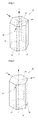
- Fig. 1 is a view describing the crystal structure of sapphire.
- Fig. 2 is a view illustrating unit cells of GaN that is a III-V group nitride compound semiconductor.
- Fig. 3 is a view illustrating atoms arranged in the C-face of a sapphire substrate.
- Fig. 4 is a view describing atoms arranged in the C-face of the sapphire substrate, and atomic arrangement of GaN.
- Fig. 5 is a view illustrating that protrusions have been formed and a GaN layer has been grown on the C-face of the sapphire substrate.
- Fig. 6 is a photograph of an optical microscope describing empty spaces formed in one sides of the protrusions on the C-face of the sapphire substrate.
- Figs. 7 and 8 are views describing a light emitting device according to an invention, and a method of manufacturing the light emitting device.
- Fig. 9 is a view describing a light emitting device package in which light emitting devices according to inventions are installed.
- Fig. 10 is a view illustrating a backlight unit including a light emitting device or light emitting device package according to an invention.
- Fig. 11 is a perspective view of a lighting unit including light emitting devices or light emitting device packages according to inventions.
- a layer (or film), a region, a pattern, or a structure is referred to as being 'on/above/over/upper' substrate or 'under/below/lower' substrate
- the 'on/above/over/upper' substrate and 'under/below/lower' substrate comprise each layer (or film), a region, a pad, or patterns, which can be directly formed on substrate as well as each layer (or film), the region, the pad, or the patterns, which can be indirectly formed under another layer (film), another region, another pad, or another patterns, with one or more intervening layers may also being present. Therefore, meaning thereof should be judged according to the spirit of the present disclosure.
- Thickness or size of each layer in the drawings has been exaggerated, omitted, or roughly illustrated for the convenience and clarity of the description. Further, sizes of the respective components do not entirely reflect actual sizes thereof.
- Fig. 1 is a view describing the crystal structure of sapphire.
- a sapphire unit cell 20 has a hexagonal structure. Positions and directions of A-plane 22, C-plane 24, M-plane 26, and R-plane 28 of the sapphire unit cell 20 are disclosed in Fig. 1 .
- the A-plane 22 is perpendicular to the C-plane 24, and the M-plane 26 forms a side of the sapphire unit cell 20.
- the R-plane 28 is inclined to an angle of 57.6 with respect to the C-plane 24.
- the sapphire unit cell 20 has an a1-axis, an a2-axis, and an a3-axis which cross one another to an angle of 120 degrees on the same plane, and a c-axis which is perpendicular to the plane.
- Fig. 2 is a view illustrating unit cells of GaN that is a III-V group nitride compound semiconductor.
- a GaN unit cell 30 has a hexagonal structure, and includes M-planes 36 that form sides of the GaN unit cell 30, C-planes 34 that form C-faces of the top side and the bottom side, and A-planes 32 that are perpendicular to the C-planes 34.
- M-planes 36 that form sides of the GaN unit cell 30
- C-planes 34 that form C-faces of the top side and the bottom side
- A-planes 32 that are perpendicular to the C-planes 34.
- the M-planes 36 of the GaN on the sapphire are exposed if the A-planes 32 of the sapphire are exposed.
- the A-face of the sapphire is parallel to the M-face of the GaN.
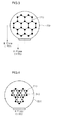
- Fig. 3 is a view illustrating atoms arranged in the C-face of a sapphire substrate
- Fig. 4 is a view describing atoms arranged in the C-face of the sapphire substrate, and atomic arrangement of GaN.
- An atomic arrangement 210 of sapphire formed on the C-face of the sapphire substrate 200 is illustrated in Figs. 3 and 4
- an atomic arrangement 310 of GaN formed on the C-face of the sapphire substrate 200 is illustrated in Fig. 4
- the GaN layer is grown as the atomic arrangement 310 of GaN is being twisted to an angle of 30 degrees with respect to the atomic arrangement 210 of sapphire as illustrated in Fig. 4 .
- the GaN layer When growing the GaN layer on the C-face of the sapphire substrate 200, the GaN layer is grown in the C-face direction. However, the A-face of the GaN layer is grown in a way that the A-face of the GaN layer corresponds to the M-face of the C-face of the sapphire substrate 200, and the M-face of the GaN layer is grown in a way that the M-face of the GaN layer corresponds to the A-face of the C-face of the sapphire substrate 200.
- the A-face of the sapphire substrate 200 and the A-face of the GaN layer form an angle of more than 0 degree.
- the A-face of the sapphire substrate 200 and the A-face of the GaN layer may form an angle of 30 degrees.
- Fig. 5 is a view illustrating that protrusions have been formed and a GaN layer has been grown on the C-face of the sapphire substrate
- Fig. 6 is a photograph of an optical microscope describing empty spaces formed in one sides of the protrusions on the C-face of the sapphire substrate.
- the C-face of the sapphire substrate 200 is selectively removed such that one or more protrusions 220 are formed on the C-face of the sapphire substrate, and the GaN layer 300 is grown such that empty spaces 230 are formed in one side of the protrusions.
- the protrusions 220 are formed in an approximately circular planar shape as illustrated in a left enlarged view of Fig. 5 , and the protrusions 220 are formed in an approximately hemispherical cross-sectional shape including the R-face as illustrated in a right enlarged view of Fig. 5 .
- the protrusions 220 may include the R-face such that the empty spaces 230 may be formed more effectively. That is, a plane of the R-face may be formed between the highest side and the lowest side of the protrusions 220.
- the GaN layer 300 is grown in the direction from the A-face to the C-face and grown mainly in the direction from the M-face to the R-plane having semi-polarization as illustrated as arrows in the left enlarged view of Fig. 5 .
- the GaN layer 300 is grown in the direction from the R-face of the protrusions 220 to the A-face thereof and grown mainly in the direction of the C-face in the C-plane sapphire substrate 200 as illustrated as arrows in the right enlarged view of Fig. 5 .
- Empty spaces 230 are formed in sides of six portions at which M-faces of the protrusions 220 encounter as illustrated in Figs. 5 and 6 since a GaN layer 300 grown on the C-face of the sapphire substrate 200 and a GaN layer 300 grown on the protrusions 220 vary in the growth rate depending on the growth direction.
- the C-face of the sapphire substrate 200 has a refractive index of about 1.7, and the empty spaces 230 have a refractive index of about 1. Therefore, light passing through regions in which the empty spaces 230 are formed is scattered while it is being reflected and refracted by a refractive index of the C-face of the sapphire substrate 200 and that of the empty spaces 230. Accordingly, light extraction efficiency can be improved by forming the empty spaces 230 in the C-face of the sapphire substrate 200.
- Figs. 7 and 8 are views describing a light emitting device according to an invention, and a method of manufacturing the light emitting device.
- one or more protrusions 220 are formed by preparing the C-face of the sapphire substrate 200 and etching the top side of the C-face of the sapphire substrate 200, thereby selectively removing the top side of the C-face of the sapphire substrate 200.
- the protrusions 220 may be formed in such a shape that is described in Fig. 5 .
- An undoped semiconductor layer 320 and a light emitting structure layer 360 including a first conductive semiconductor layer 330, an active layer 340, and a second conductive semiconductor layer 350 are formed on the C-face of the sapphire substrate 200 in which the protrusions 220 are formed.
- the undoped semiconductor layer 320 may be formed as an undoped GaN layer.
- the empty spaces 230 are formed in one side of the protrusions 220 as described in Fig. 5 when forming a GaN-based semiconductor layer such as the undoped semiconductor layer 320 on the C-face of the sapphire substrate 200 in which the protrusions 220 are formed.
- a GaN layer may be formed on the C-face of the sapphire substrate 200 without forming the undoped semiconductor layer 320, or the first conductive semiconductor layer 330 such as a GaN layer into which first conductive impurities are injected may be directly grown.
- the empty spaces 230 are formed in one side of the protrusions 220 also in this case.
- the light emitting structure layer 360 may include plural compound semiconductor layers of group III to group V elements.
- the light emitting structure layer 360 may include a first conductive semiconductor layer 330, an active layer 340 formed on the first conductive semiconductor layer 330, and a second conductive semiconductor layer 350 formed on the active layer 340.
- the first conductive semiconductor layer 330 may include an n type semiconductor layer, wherein the n type semiconductor layer may be formed from semiconductor materials having a composition expression of In x Al y Ga 1-x-y N (0 ⁇ x ⁇ 1, 0 ⁇ y ⁇ 1, 0 ⁇ x+y ⁇ 1) selected from InAlGaN, GaN, AlGaN, AlInN, InGaN, AlN, and InN, and wherein n type dopants including Si, Ge and Sn may be doped on the n type semiconductor layer.
- the first conductive semiconductor layer 330 may be formed in a single layer or multiple layers, and the first conductive semiconductor layer 330 is not limited thereto.
- the active layer 340 is formed under the first conductive semiconductor layer 330, and may include a Single Quantum Well structure, a Multiple Quantum Well structure, a Quantum Dot structure, or a Quantum Wire structure.
- the active layer 340 may be formed from semiconductor materials having a composition expression of In x Al y Ga 1-x-y N (0 ⁇ x ⁇ 1, 0 ⁇ y ⁇ 1, 0 ⁇ x+y ⁇ 1).
- the active layer 340 may be formed by laying up plural well layers and plural barrier layers. For instance, an InGaN well layer and a GaN barrier layer are periodically laid up to form the active layer 340.
- a clad layer (which is not shown in drawings) formed by doping an n type or p type dopant on the top and/or bottom of the active layer 340 may be formed, and the clad layer (which is not shown in drawings) may be embodied into an AlGaN layer or InAlGaN layer.
- the second conductive semiconductor layer 350 is formed under the active layer 340 and may be embodied into a p type semiconductor layer, wherein the p type semiconductor layer may be formed from semiconductor materials having a composition expression of In x Al y Ga 1-x-y N (0 ⁇ x ⁇ 1, 0 ⁇ y ⁇ 1, 0 ⁇ x+y ⁇ 1) selected from InAlGaN, GaN, AlGaN, InGaN, AlInN, AlN, and InN, and wherein p type dopants including Mg, Zn, Ca, Sr, and Ba may be doped on the p type semiconductor layer.
- the p type semiconductor layer may be formed from semiconductor materials having a composition expression of In x Al y Ga 1-x-y N (0 ⁇ x ⁇ 1, 0 ⁇ y ⁇ 1, 0 ⁇ x+y ⁇ 1) selected from InAlGaN, GaN, AlGaN, InGaN, AlInN, AlN, and InN, and wherein p type dopants including Mg, Zn, Ca, Sr,
- the second conductive semiconductor layer 350 may be formed in a single layer or multiple layers, and the second conductive semiconductor layer 350 is not limited thereto.
- the first conductive semiconductor layer 330 may include a p type semiconductor layer
- the second conductive semiconductor layer 350 may include an n type semiconductor layer in the light emitting structure layer 360 differently from the light emitting structure layer 360 described above.
- a third conductive semiconductor layer (which is not shown in drawings) including an n type or p type semiconductor layer may be formed on the second conductive semiconductor layer 350.
- the light emitting structure layer 360 may have one or more of np, pn, npn, and pnp junction structures.
- a conductive dopant within the first conductive semiconductor layer 330 and the second conductive semiconductor layer 350 may be formed in a uniform or non-uniform doping concentration. Namely, the light emitting structure layer 360 may be constructed in various structures, and the light emitting structure layer 360 is not limited thereto.
- the light emitting structure layer 360 is selectively removed such that the first conductive semiconductor layer 330 is partially exposed in the upward direction. Then a first electrode unit 170 is formed on the first conductive semiconductor layer 330, and a second electrode unit 180 is formed on the second conductive semiconductor layer 350. Therefore, a light emitting device according to an invention may be fabricated.
- Fig. 9 is a view describing a light emitting device package in which light emitting devices according to inventions are installed.
- a light emitting device package includes a package body 600, a first electrode 610 and a second electrode 620 installed on the package body 600, a light emitting device 100 installed on the package body 600 and electrically connected to the first electrode 610 and second electrode 620, and a molding member 500 surrounding the light emitting device 100.
- the package body 600 may be formed from material selected from silicon, synthetic resins, and metals, and an inclined plane may be formed around the light emitting device 100.
- the first electrode 610 and second electrode 620 are electrically separated from each other and play a role of providing the light emitting device 100 with the power supply. Further, the first electrode 610 and second electrode 620 may play a role of increasing light efficiency by reflecting light generated from the light emitting device 100, or may play a role of emitting heat generated from the light emitting device 100 to the outside.
- the light emitting device 100 may be installed on the package body 600, or on the first electrode 610 or second electrode 620.
- the light emitting device 100 may be electrically connected to the first electrode 610 and second electrode 620 through a wire 400.
- the molding member 500 may protect the light emitting device 100 by surrounding the light emitting device 100. Further, the molding member 500 comprises a phosphor to vary wavelength of light emitted from the light emitting device 100.
- Plural light emitting device packages according to an invention may be arrayed on a board, and optical members such as light guide plate, prism sheet, diffusion sheet, and fluorescent sheet may be arranged in the path of lights emitted from the light emitting device packages.
- optical members such as light guide plate, prism sheet, diffusion sheet, and fluorescent sheet may be arranged in the path of lights emitted from the light emitting device packages.
- Such light emitting device package, board, and optical member may function as a back light unit or lighting unit.
- a lighting system may include a back light unit, a lighting unit, an indication unit, a lamp, and a street lamp.
- Fig. 10 is a view illustrating a backlight unit including a light emitting device or light emitting device package according to an invention, wherein a back light unit 1100 of Fig. 10 is an example of the lighting system, and the back light unit is not limited thereto.
- the back light unit 1100 may include a bottom frame 1140, a light guide member 1120 arranged within the bottom frame 1140, and a light emitting module 1110 arranged on at least one of the side and bottom of the light guide member 1120. Additionally, a reflective sheet 1130 may be arranged under the light guide member 1120.
- the bottom frame 1140 may be formed from such materials as metals and resins, and formed in a box shape of which the top is opened such that the light guide member 1120, back light unit 1100, and reflective sheet 1130 may be housed in bottom frame 1140, the bottom frame 1140 is not limited thereto.
- the light emitting module 1110 may include a board 300, and plural light emitting device packages 200 according to inventions mounted on the board 300.
- the plural light emitting device packages 200 are capable of supplying light to the light guide member 1120.
- the light emitting module 1110 may be arranged on at least one of inner sides of the bottom frame 1140, and light is capable of being supplied toward at least one side of the light guide member 1120 accordingly.
- the light emitting module 1110 is arranged under the bottom frame 1140 to supply light toward the bottom of the light guide member 1120, and arrangement of the light emitting module 1110 is not limited thereto since the arrangement of the light emitting module 1110 is capable of being diversely varied according to design of the back light unit 1100.
- the light guide member 1120 may be arranged within the bottom frame 1140.
- the light guide member 1120 is capable of guiding the light to a display panel (which is not shown in drawings) after subjecting light supplied from the light emitting module 1110 to surface light source conversion.
- the light guide member 1120 may be a light guide plate (LGP).
- the light guide plate may be formed from one selected from acrylic resins such as polymethyl metaacrylate (PMMA), and polyethylene terephthalate (PET), polycarbonate (PC), cyclic olefin copolymer (COC), and polyethylene naphthalate (PEN).
- PMMA polymethyl metaacrylate
- PET polyethylene terephthalate
- PC polycarbonate
- COC cyclic olefin copolymer
- PEN polyethylene naphthalate
- An optical sheet 1150 may be arranged on the top of the light guide member 1120.
- the optical sheet 1150 may include at least one of a diffusion sheet, a light collection sheet, a brightness enhanced sheet, and a fluorescence sheet.
- the optical sheet 1150 may be formed by laying up the diffusion sheet, light collection sheet, brightness enhanced sheet, and fluorescence sheet.
- the diffusion sheet 1150 evenly diffuses light emitted from the light emitting module 1110, and the diffused light can be collected into a display panel (which is not illustrated in drawings) by the light collection sheet.
- Light emitted from the light collection sheet is randomly polarized light, wherein the brightness enhanced sheet is capable of increasing degree of polarization of the light emitted from the light collection sheet.
- the light collection sheet may be a horizontal prism sheet or/and a vertical prism sheet.
- the brightness enhanced sheet may be a dual brightness enhancement film.
- the fluorescence sheet may be a light-transmitting plate or film comprising a phosphor.
- the reflective sheet 1130 may be arranged under the light guide member 1120.
- the reflective sheet 1130 is capable of reflecting light emitted through the bottom of the light guide member 1120 toward the emitting surface of the light guide member 1120.
- the reflective sheet 1130 may be formed from resins such as PET, PC, and PVC, the resins of the reflective sheet 1130 are not limited thereto.
- Fig. 11 is a perspective view of a lighting unit including light emitting devices or light emitting device packages according to inventions, wherein a lighting unit 1200 of Fig. 11 is an example of the lighting system, and the lighting system is not limited thereto.
- the lighting unit 1200 may include a case body 1210, a light emitting module 1230 installed in the case body 1210, and a connecting terminal 1220 installed on the case body 1210 to receive a power source from the external power supply.
- the case body 1210 is formed from material having good heat dissipation properties, and the case body 1210 may be formed from materials such as metals and resins.
- the light emitting module 1230 may include a board 300, and one or more light emitting device packages 200 according to an invention mounted on the board 300.
- the board 300 may be an insulator on which circuit patterns are printed, and examples of the board 300 may include an ordinary printed circuit board (PCB), a metal core PCB, a flexible PCB, and a ceramic PCB.
- PCB printed circuit board
- metal core PCB metal core PCB
- flexible PCB flexible PCB
- ceramic PCB ceramic PCB
- the board 300 may be formed from material that reflects light efficiently, or may be formed in colors including white and silver such that the surface of the board 300 having those colors is reflected efficiently.
- One or more light emitting device packages 200 according to an invention may be mounted on the board 300.
- Each of the light emitting device packages 200 may include one or more light emitting devices according to an invention, and the light emitting devices may be light emitting diodes (LEDs).
- the light emitting diodes may include colored light emitting diodes which emit colored lights such as red, green, blue, and white lights, and UV light emitting diodes which emit ultraviolet rays.
- the light emitting module 1230 may be arranged such that the light emitting module 1230 has a combination of various light emitting diodes in order to obtain color sense and brightness. For instance, a combination of a white light emitting diode, a red light emitting diode, and a green light emitting diode may be arranged in the light emitting module 1230 to secure high color rendering index (CRI). Further, a fluorescence sheet may be additionally arranged in the proceeding path of light emitted from the light emitting module 1230, and the fluorescence sheet changes wavelength of the light emitted from the light emitting module 1230.
- CRI color rendering index
- the fluorescence sheet may include a yellow phosphor, and the light emitted from the light emitting module 1230 may be finally shown as white light after passing through the fluorescence sheet.
- the connecting terminal 1220 is electrically connected to the light emitting module 1230 such that the connecting terminal 1220 can supply a power source to the light emitting module 1230.
- the connecting terminal 1220 is a socket type connecting terminal which is turned and inserted into an external power supply such that the connecting terminal is coupled to the power supply
- the connecting terminal 1220 is not limited thereto.
- the connecting terminal 1220 is formed in a pin shape such that the connecting terminal 1220 may be inserted into the external power supply, or may be connected to the external power supply by wiring.
- the foregoing lighting system can obtain desired optical effects by arranging one or more of a light guide member, a diffusion sheet, a light collection sheet, a brightness enhanced sheet, and a fluorescence sheet in the proceeding path of the light emitted from the light emitting module.
- a lighting system according to inventions is capable of possessing excellent light characteristics by comprising light emitting devices or light emitting device packages according to the inventions.
- any reference in this specification to "one embodiment,” “an embodiment,” “example embodiment,” etc. means that a particular feature, structure, or characteristic described in connection with the embodiment is included in at least one embodiment of the invention.
- the appearances of such phrases in various places in the specification are not necessarily all referring to the same embodiment.
Landscapes
- Led Devices (AREA)
- Non-Portable Lighting Devices Or Systems Thereof (AREA)
- Led Device Packages (AREA)
Abstract
Description
- The present application claims priority OF Korean Patent Application No.
10-2010-0010205 filed on February 04, 2010 - The present disclosure relates to a light emitting device, a light emitting device package, and a lighting system.
- Light Emitting Diodes (LEDs) are frequently used as the light emitting device.
- The LEDs are a semiconductor light emitting device which transforms electric current into light.
- Wavelengths of light emitted from such LEDs vary according to semiconductor materials used in manufacturing the LEDs. This is so since the wavelengths of the emitted light vary according to band-gaps of the semiconductor materials representing energy differences between valence band electrons and conduction band electrons.
- Brightness of the LEDs has been gradually increased such that the LEDs are used as light sources for displays, automobiles, and lighting, and it is possible to realize LEDs emitting white light with excellent efficiency by using phosphor or combining LEDs of various colors.
- The present inventions provide a light emitting device, a light emitting device package, and a lighting system.
- The present inventions also provide a light emitting device with improved light extraction efficiency, a light emitting device package, and a lighting system.
- A light emitting device according to one invention includes: a substrate which has protrusions on the C-face, and of which unit cells are constructed in a hexagonal structure; a semiconductor layer which is formed on the substrate, in which empty spaces are formed in sides of the protrusions, and of which unit cells are constructed in a hexagonal structure; and a light emitting structure layer comprising a first conductive semiconductor layer, a second conductive semiconductor layer, and an active layer formed between the first conductive semiconductor layer and second conductive semiconductor layer which are formed on the semiconductor layer, wherein the A-face of the substrate and the A-face of the semiconductor layer form an angle of greater than zero degree, and the protrusions include the R-faces.
- A light emitting device package according to another invention includes: a package body; a first electrode and a second electrode electrically separated from each other on the package body; a light emitting device electrically connected to the first electrode and second electrode on the package body; and a molding member surrounding the light emitting device on the package body, wherein the light emitting device includes: a substrate which has protrusions on the C-face, and of which unit cells are constructed in a hexagonal structure; a semiconductor layer which is formed on the substrate, in which empty spaces are formed in sides of the protrusions, and of which unit cells are constructed in a hexagonal structure; and a light emitting structure layer comprising a first conductive semiconductor layer, a second conductive semiconductor layer, and an active layer formed between the first conductive semiconductor layer and second conductive semiconductor layer which are formed on the semiconductor layer, wherein the A-face of the substrate and the A-face of the semiconductor layer form an angle of greater than zero degree, and the protrusions include the R-faces.
- A lighting system using light emitting devices as a light source according to still further another invention includes a light emitting module comprising one or more light emitting devices, wherein the light emitting device includes: a substrate which has protrusions on the C-face, and of which unit cells are constructed in a hexagonal structure; a semiconductor layer which is formed on the substrate, in which empty spaces are formed in sides of the protrusions, and of which unit cells are constructed in a hexagonal structure; and a light emitting structure layer comprising a first conductive semiconductor layer, a second conductive semiconductor layer, and an active layer formed between the first conductive semiconductor layer and second conductive semiconductor layer which are formed on the semiconductor layer, wherein the A-face of the substrate and the A-face of the semiconductor layer form an angle of greater than zero degree, and the protrusions include the R-faces.
- The details of one or more embodiments are set forth in the accompanying drawings and the description below. Other features will be apparent from the description and drawings, and from the claims.
-
Fig. 1 is a view describing the crystal structure of sapphire. -
Fig. 2 is a view illustrating unit cells of GaN that is a III-V group nitride compound semiconductor. -
Fig. 3 is a view illustrating atoms arranged in the C-face of a sapphire substrate. -
Fig. 4 is a view describing atoms arranged in the C-face of the sapphire substrate, and atomic arrangement of GaN. -
Fig. 5 is a view illustrating that protrusions have been formed and a GaN layer has been grown on the C-face of the sapphire substrate. -
Fig. 6 is a photograph of an optical microscope describing empty spaces formed in one sides of the protrusions on the C-face of the sapphire substrate. -
Figs. 7 and 8 are views describing a light emitting device according to an invention, and a method of manufacturing the light emitting device. -
Fig. 9 is a view describing a light emitting device package in which light emitting devices according to inventions are installed. -
Fig. 10 is a view illustrating a backlight unit including a light emitting device or light emitting device package according to an invention. -
Fig. 11 is a perspective view of a lighting unit including light emitting devices or light emitting device packages according to inventions. - Reference will now be made in detail to the embodiments of the present disclosure, examples of which are illustrated in the accompanying drawings.
A light emitting device according to an invention will be described in detail with reference to the accompanying drawings. The invention may, however, be embodied in many different forms and should not be construed as being limited to the embodiments set forth herein; rather, that alternate embodiments included in other retrogressive inventions or falling within the spirit and scope of the present disclosure can easily be derived through adding, altering, and changing, and will fully convey the concept of the invention to those skilled in the art. - In the descriptions of inventions, it will be understood that when a layer (or film), a region, a pattern, or a structure is referred to as being 'on/above/over/upper' substrate or 'under/below/lower' substrate, the 'on/above/over/upper' substrate and 'under/below/lower' substrate comprise each layer (or film), a region, a pad, or patterns, which can be directly formed on substrate as well as each layer (or film), the region, the pad, or the patterns, which can be indirectly formed under another layer (film), another region, another pad, or another patterns, with one or more intervening layers may also being present. Therefore, meaning thereof should be judged according to the spirit of the present disclosure.
- Thickness or size of each layer in the drawings has been exaggerated, omitted, or roughly illustrated for the convenience and clarity of the description. Further, sizes of the respective components do not entirely reflect actual sizes thereof.
- Hereinafter, light emitting devices and light emitting device packages according to inventions are described in detail by referring to the attached drawings.
-
Fig. 1 is a view describing the crystal structure of sapphire. - A sapphire unit cell 20 has a hexagonal structure. Positions and directions of A-plane 22, C-plane 24, M-plane 26, and R-plane 28 of the sapphire unit cell 20 are disclosed in
Fig. 1 . TheA-plane 22 is perpendicular to the C-plane 24, and the M-plane 26 forms a side of the sapphire unit cell 20. The R-plane 28 is inclined to an angle of 57.6 with respect to the C-plane 24. The sapphire unit cell 20 has an a1-axis, an a2-axis, and an a3-axis which cross one another to an angle of 120 degrees on the same plane, and a c-axis which is perpendicular to the plane. -
Fig. 2 is a view illustrating unit cells of GaN that is a III-V group nitride compound semiconductor. - A GaN unit cell 30 has a hexagonal structure, and includes M-
planes 36 that form sides of the GaN unit cell 30, C-planes 34 that form C-faces of the top side and the bottom side, and A-planes 32 that are perpendicular to the C-planes 34. When growing GaN on such a C-face of sapphire, the GaN is grown in a way that lattice arrangement of GaN is angled to an angle of 30 degrees with respect to that of sapphire. Namely, when cutting a sapphire in which the GaN has been grown in a direction that is perpendicular to the C-face, the M-planes 36 of the GaN on the sapphire are exposed if the A-planes 32 of the sapphire are exposed. The A-face of the sapphire is parallel to the M-face of the GaN. -
Fig. 3 is a view illustrating atoms arranged in the C-face of a sapphire substrate, andFig. 4 is a view describing atoms arranged in the C-face of the sapphire substrate, and atomic arrangement of GaN. - An
atomic arrangement 210 of sapphire formed on the C-face of thesapphire substrate 200 is illustrated inFigs. 3 and 4 , and anatomic arrangement 310 of GaN formed on the C-face of thesapphire substrate 200 is illustrated inFig. 4 - Since Ga atoms are positioned such that lattice-mismatch is less occurred when growing a GaN layer on the C-face of the
sapphire substrate 200, the GaN layer is grown as theatomic arrangement 310 of GaN is being twisted to an angle of 30 degrees with respect to theatomic arrangement 210 of sapphire as illustrated inFig. 4 . - When growing the GaN layer on the C-face of the
sapphire substrate 200, the GaN layer is grown in the C-face direction. However, the A-face of the GaN layer is grown in a way that the A-face of the GaN layer corresponds to the M-face of the C-face of thesapphire substrate 200, and the M-face of the GaN layer is grown in a way that the M-face of the GaN layer corresponds to the A-face of the C-face of thesapphire substrate 200. - Further, the A-face of the
sapphire substrate 200 and the A-face of the GaN layer form an angle of more than 0 degree. For instance, the A-face of thesapphire substrate 200 and the A-face of the GaN layer may form an angle of 30 degrees. -
Fig. 5 is a view illustrating that protrusions have been formed and a GaN layer has been grown on the C-face of the sapphire substrate, andFig. 6 is a photograph of an optical microscope describing empty spaces formed in one sides of the protrusions on the C-face of the sapphire substrate. - The C-face of the
sapphire substrate 200 is selectively removed such that one ormore protrusions 220 are formed on the C-face of the sapphire substrate, and theGaN layer 300 is grown such thatempty spaces 230 are formed in one side of the protrusions. - The
protrusions 220 are formed in an approximately circular planar shape as illustrated in a left enlarged view ofFig. 5 , and theprotrusions 220 are formed in an approximately hemispherical cross-sectional shape including the R-face as illustrated in a right enlarged view ofFig. 5 . Theprotrusions 220 may include the R-face such that theempty spaces 230 may be formed more effectively. That is, a plane of the R-face may be formed between the highest side and the lowest side of theprotrusions 220. - When growing a
GaN layer 300 on the C-face of thesapphire substrate 200 having an approximately circular planar shape as illustrated in the left enlarged view ofFig. 5 , theGaN layer 300 is grown in the direction from the A-face to the C-face and grown mainly in the direction from the M-face to the R-plane having semi-polarization as illustrated as arrows in the left enlarged view ofFig. 5 . - Further, when growing the
GaN layer 300 on the C-face of thesapphire substrate 200 having an approximately hemispherical cross-sectional shape as illustrated in the right enlarged view ofFig. 5 , theGaN layer 300 is grown in the direction from the R-face of theprotrusions 220 to the A-face thereof and grown mainly in the direction of the C-face in the C-plane sapphire substrate 200 as illustrated as arrows in the right enlarged view ofFig. 5 . -
Empty spaces 230 are formed in sides of six portions at which M-faces of theprotrusions 220 encounter as illustrated inFigs. 5 and 6 since aGaN layer 300 grown on the C-face of thesapphire substrate 200 and aGaN layer 300 grown on theprotrusions 220 vary in the growth rate depending on the growth direction. - The C-face of the
sapphire substrate 200 has a refractive index of about 1.7, and theempty spaces 230 have a refractive index of about 1. Therefore, light passing through regions in which theempty spaces 230 are formed is scattered while it is being reflected and refracted by a refractive index of the C-face of thesapphire substrate 200 and that of theempty spaces 230. Accordingly, light extraction efficiency can be improved by forming theempty spaces 230 in the C-face of thesapphire substrate 200. -
Figs. 7 and 8 are views describing a light emitting device according to an invention, and a method of manufacturing the light emitting device. - Referring to
Fig. 7 , one ormore protrusions 220 are formed by preparing the C-face of thesapphire substrate 200 and etching the top side of the C-face of thesapphire substrate 200, thereby selectively removing the top side of the C-face of thesapphire substrate 200. Theprotrusions 220 may be formed in such a shape that is described inFig. 5 . - An
undoped semiconductor layer 320 and a light emittingstructure layer 360 including a firstconductive semiconductor layer 330, anactive layer 340, and a secondconductive semiconductor layer 350 are formed on the C-face of thesapphire substrate 200 in which theprotrusions 220 are formed. - For instance, the
undoped semiconductor layer 320 may be formed as an undoped GaN layer. - The
empty spaces 230 are formed in one side of theprotrusions 220 as described inFig. 5 when forming a GaN-based semiconductor layer such as theundoped semiconductor layer 320 on the C-face of thesapphire substrate 200 in which theprotrusions 220 are formed. - Further, a GaN layer may be formed on the C-face of the
sapphire substrate 200 without forming theundoped semiconductor layer 320, or the firstconductive semiconductor layer 330 such as a GaN layer into which first conductive impurities are injected may be directly grown. Theempty spaces 230 are formed in one side of theprotrusions 220 also in this case. - The light emitting
structure layer 360 may include plural compound semiconductor layers of group III to group V elements. For instance, the light emittingstructure layer 360 may include a firstconductive semiconductor layer 330, anactive layer 340 formed on the firstconductive semiconductor layer 330, and a secondconductive semiconductor layer 350 formed on theactive layer 340. - For instance, the first
conductive semiconductor layer 330 may include an n type semiconductor layer, wherein the n type semiconductor layer may be formed from semiconductor materials having a composition expression of InxAlyGa1-x-yN (0≤x≤1, 0≤y≤1, 0≤x+y≤1) selected from InAlGaN, GaN, AlGaN, AlInN, InGaN, AlN, and InN, and wherein n type dopants including Si, Ge and Sn may be doped on the n type semiconductor layer. The firstconductive semiconductor layer 330 may be formed in a single layer or multiple layers, and the firstconductive semiconductor layer 330 is not limited thereto. - The
active layer 340 is formed under the firstconductive semiconductor layer 330, and may include a Single Quantum Well structure, a Multiple Quantum Well structure, a Quantum Dot structure, or a Quantum Wire structure. Theactive layer 340 may be formed from semiconductor materials having a composition expression of InxAlyGa1-x-yN (0≤x≤1, 0≤y≤1, 0≤x+y≤1). When theactive layer 340 is formed in the Multiple Quantum Well structure, theactive layer 340 may be formed by laying up plural well layers and plural barrier layers. For instance, an InGaN well layer and a GaN barrier layer are periodically laid up to form theactive layer 340. - A clad layer (which is not shown in drawings) formed by doping an n type or p type dopant on the top and/or bottom of the
active layer 340 may be formed, and the clad layer (which is not shown in drawings) may be embodied into an AlGaN layer or InAlGaN layer. - For instance, the second
conductive semiconductor layer 350 is formed under theactive layer 340 and may be embodied into a p type semiconductor layer, wherein the p type semiconductor layer may be formed from semiconductor materials having a composition expression of InxAlyGa1-x-yN (0≤x≤1, 0≤y≤1, 0≤x+y≤1) selected from InAlGaN, GaN, AlGaN, InGaN, AlInN, AlN, and InN, and wherein p type dopants including Mg, Zn, Ca, Sr, and Ba may be doped on the p type semiconductor layer. - The second
conductive semiconductor layer 350 may be formed in a single layer or multiple layers, and the secondconductive semiconductor layer 350 is not limited thereto. - On the other hand, the first
conductive semiconductor layer 330 may include a p type semiconductor layer, and the secondconductive semiconductor layer 350 may include an n type semiconductor layer in the light emittingstructure layer 360 differently from the light emittingstructure layer 360 described above. Further, a third conductive semiconductor layer (which is not shown in drawings) including an n type or p type semiconductor layer may be formed on the secondconductive semiconductor layer 350. Accordingly, the light emittingstructure layer 360 may have one or more of np, pn, npn, and pnp junction structures. Further, a conductive dopant within the firstconductive semiconductor layer 330 and the secondconductive semiconductor layer 350 may be formed in a uniform or non-uniform doping concentration. Namely, the light emittingstructure layer 360 may be constructed in various structures, and the light emittingstructure layer 360 is not limited thereto. - Referring to
Fig. 8 , the light emittingstructure layer 360 is selectively removed such that the firstconductive semiconductor layer 330 is partially exposed in the upward direction. Then afirst electrode unit 170 is formed on the firstconductive semiconductor layer 330, and asecond electrode unit 180 is formed on the secondconductive semiconductor layer 350. Therefore, a light emitting device according to an invention may be fabricated. - In the foregoing light emitting device, light is generated from the
active layer 340 as the power supply is being applied to thefirst electrode unit 170 and thesecond electrode unit 180, and a portion of the light generated from theactive layer 340 is proceeded in the direction of the C-face of thesapphire substrate 200 such that the portion of the light is reflected, refracted, and scattered in theempty spaces 230. Therefore, the scattered light is extracted more effectively to the outside of the light emitting device such that light efficiency of the light emitting device can be improved. -
Fig. 9 is a view describing a light emitting device package in which light emitting devices according to inventions are installed. - Referring to
Fig. 9 , a light emitting device package according to an invention includes a package body 600, a first electrode 610 and asecond electrode 620 installed on the package body 600, a light emitting device 100 installed on the package body 600 and electrically connected to the first electrode 610 andsecond electrode 620, and amolding member 500 surrounding the light emitting device 100. - The package body 600 may be formed from material selected from silicon, synthetic resins, and metals, and an inclined plane may be formed around the light emitting device 100.
- The first electrode 610 and
second electrode 620 are electrically separated from each other and play a role of providing the light emitting device 100 with the power supply. Further, the first electrode 610 andsecond electrode 620 may play a role of increasing light efficiency by reflecting light generated from the light emitting device 100, or may play a role of emitting heat generated from the light emitting device 100 to the outside. - The light emitting device 100 may be installed on the package body 600, or on the first electrode 610 or
second electrode 620. - The light emitting device 100 may be electrically connected to the first electrode 610 and
second electrode 620 through awire 400. - The
molding member 500 may protect the light emitting device 100 by surrounding the light emitting device 100. Further, themolding member 500 comprises a phosphor to vary wavelength of light emitted from the light emitting device 100. - Plural light emitting device packages according to an invention may be arrayed on a board, and optical members such as light guide plate, prism sheet, diffusion sheet, and fluorescent sheet may be arranged in the path of lights emitted from the light emitting device packages. Such light emitting device package, board, and optical member may function as a back light unit or lighting unit. For instance, a lighting system may include a back light unit, a lighting unit, an indication unit, a lamp, and a street lamp.
-
Fig. 10 is a view illustrating a backlight unit including a light emitting device or light emitting device package according to an invention, wherein aback light unit 1100 ofFig. 10 is an example of the lighting system, and the back light unit is not limited thereto. - Referring to
Fig. 10 , theback light unit 1100 may include abottom frame 1140, alight guide member 1120 arranged within thebottom frame 1140, and alight emitting module 1110 arranged on at least one of the side and bottom of thelight guide member 1120. Additionally, areflective sheet 1130 may be arranged under thelight guide member 1120. - Although the
bottom frame 1140 may be formed from such materials as metals and resins, and formed in a box shape of which the top is opened such that thelight guide member 1120, backlight unit 1100, andreflective sheet 1130 may be housed inbottom frame 1140, thebottom frame 1140 is not limited thereto. - The
light emitting module 1110 may include aboard 300, and plural light emitting device packages 200 according to inventions mounted on theboard 300. The plural light emitting device packages 200 are capable of supplying light to thelight guide member 1120. - As illustrated in
Fig. 10 , thelight emitting module 1110 may be arranged on at least one of inner sides of thebottom frame 1140, and light is capable of being supplied toward at least one side of thelight guide member 1120 accordingly. - The
light emitting module 1110 is arranged under thebottom frame 1140 to supply light toward the bottom of thelight guide member 1120, and arrangement of thelight emitting module 1110 is not limited thereto since the arrangement of thelight emitting module 1110 is capable of being diversely varied according to design of theback light unit 1100. - The
light guide member 1120 may be arranged within thebottom frame 1140. Thelight guide member 1120 is capable of guiding the light to a display panel (which is not shown in drawings) after subjecting light supplied from thelight emitting module 1110 to surface light source conversion. - For instance, the
light guide member 1120 may be a light guide plate (LGP). The light guide plate may be formed from one selected from acrylic resins such as polymethyl metaacrylate (PMMA), and polyethylene terephthalate (PET), polycarbonate (PC), cyclic olefin copolymer (COC), and polyethylene naphthalate (PEN). - An optical sheet 1150 may be arranged on the top of the
light guide member 1120. - Examples of the optical sheet 1150 may include at least one of a diffusion sheet, a light collection sheet, a brightness enhanced sheet, and a fluorescence sheet. For example, the optical sheet 1150 may be formed by laying up the diffusion sheet, light collection sheet, brightness enhanced sheet, and fluorescence sheet. In this case, the diffusion sheet 1150 evenly diffuses light emitted from the
light emitting module 1110, and the diffused light can be collected into a display panel (which is not illustrated in drawings) by the light collection sheet. Light emitted from the light collection sheet is randomly polarized light, wherein the brightness enhanced sheet is capable of increasing degree of polarization of the light emitted from the light collection sheet. For instance, the light collection sheet may be a horizontal prism sheet or/and a vertical prism sheet. Further, the brightness enhanced sheet may be a dual brightness enhancement film. Further, the fluorescence sheet may be a light-transmitting plate or film comprising a phosphor. - The
reflective sheet 1130 may be arranged under thelight guide member 1120. Thereflective sheet 1130 is capable of reflecting light emitted through the bottom of thelight guide member 1120 toward the emitting surface of thelight guide member 1120. - Although the
reflective sheet 1130 may be formed from resins such as PET, PC, and PVC, the resins of thereflective sheet 1130 are not limited thereto. -
Fig. 11 is a perspective view of a lighting unit including light emitting devices or light emitting device packages according to inventions, wherein alighting unit 1200 ofFig. 11 is an example of the lighting system, and the lighting system is not limited thereto. - Referring to
Fig. 11 , thelighting unit 1200 may include acase body 1210, a light emitting module 1230 installed in thecase body 1210, and a connecting terminal 1220 installed on thecase body 1210 to receive a power source from the external power supply. - Preferably, the
case body 1210 is formed from material having good heat dissipation properties, and thecase body 1210 may be formed from materials such as metals and resins. - The light emitting module 1230 may include a
board 300, and one or more light emitting device packages 200 according to an invention mounted on theboard 300. - The
board 300 may be an insulator on which circuit patterns are printed, and examples of theboard 300 may include an ordinary printed circuit board (PCB), a metal core PCB, a flexible PCB, and a ceramic PCB. - Further, the
board 300 may be formed from material that reflects light efficiently, or may be formed in colors including white and silver such that the surface of theboard 300 having those colors is reflected efficiently. - One or more light emitting device packages 200 according to an invention may be mounted on the
board 300. Each of the light emitting device packages 200 may include one or more light emitting devices according to an invention, and the light emitting devices may be light emitting diodes (LEDs). The light emitting diodes may include colored light emitting diodes which emit colored lights such as red, green, blue, and white lights, and UV light emitting diodes which emit ultraviolet rays. - The light emitting module 1230 may be arranged such that the light emitting module 1230 has a combination of various light emitting diodes in order to obtain color sense and brightness. For instance, a combination of a white light emitting diode, a red light emitting diode, and a green light emitting diode may be arranged in the light emitting module 1230 to secure high color rendering index (CRI). Further, a fluorescence sheet may be additionally arranged in the proceeding path of light emitted from the light emitting module 1230, and the fluorescence sheet changes wavelength of the light emitted from the light emitting module 1230. If the light emitted from the light emitting module 1230 has a blue wavelength range, the fluorescence sheet may include a yellow phosphor, and the light emitted from the light emitting module 1230 may be finally shown as white light after passing through the fluorescence sheet.
- The connecting terminal 1220 is electrically connected to the light emitting module 1230 such that the connecting terminal 1220 can supply a power source to the light emitting module 1230. Although the connecting terminal 1220 is a socket type connecting terminal which is turned and inserted into an external power supply such that the connecting terminal is coupled to the power supply, the connecting terminal 1220 is not limited thereto. For instance, the connecting terminal 1220 is formed in a pin shape such that the connecting terminal 1220 may be inserted into the external power supply, or may be connected to the external power supply by wiring.
- The foregoing lighting system can obtain desired optical effects by arranging one or more of a light guide member, a diffusion sheet, a light collection sheet, a brightness enhanced sheet, and a fluorescence sheet in the proceeding path of the light emitted from the light emitting module.
- As described above, a lighting system according to inventions is capable of possessing excellent light characteristics by comprising light emitting devices or light emitting device packages according to the inventions.
- Any reference in this specification to "one embodiment," "an embodiment," "example embodiment," etc., means that a particular feature, structure, or characteristic described in connection with the embodiment is included in at least one embodiment of the invention. The appearances of such phrases in various places in the specification are not necessarily all referring to the same embodiment. Further, when a particular feature, structure, or characteristic is described in connection with any embodiment, it is submitted that it is within the purview of one skilled in the art to effect such feature, structure, or characteristic in connection with other ones of the embodiments.
- Although embodiments have been described with reference to a number of illustrative embodiments thereof, it should be understood that numerous other modifications and embodiments can be devised by those skilled in the art that will fall within the spirit and scope of the principles of this disclosure. More particularly, various variations and modifications are possible in the component parts and/or arrangements of the subject combination arrangement within the scope of the disclosure, the drawings and the appended claims. In addition to variations and modifications in the component parts and/or arrangements, alternative uses will also be apparent to those skilled in the art.
Claims (15)
- A light emitting device including:a substrate which has protrusions on the C-face, and of which unit cells are constructed in a hexagonal structure;a semiconductor layer which is formed on the substrate, in which empty spaces are formed in sides of the protrusions, and of which unit cells are constructed in a hexagonal structure; anda light emitting structure layer comprising a first conductive semiconductor layer, a second conductive semiconductor layer and an active layer formed between the first conductive semiconductor layer and second conductive semiconductor layer which are formed on the semiconductor layer, wherein the A-face of the substrate and the A-face of the semiconductor layer form an angle of greater than zero degree, and the protrusions include the R-faces.
- The light emitting device according to claim 1, wherein the protrusions are formed in a hemispherical shape.
- The light emitting device according to claim 1, wherein the empty spaces are formed in plural portions on the side of the protrusions.
- The light emitting device according to claim 3, wherein the empty spaces are formed in six portions on the side of the protrusions.
- The light emitting device according to claim 1, wherein the empty spaces are formed in portions where M-faces of the protrusions encounter with one another.
- The light emitting device according to claim 1, wherein the semiconductor layer is an undoped GaN layer.
- The light emitting device according to claim 1, wherein the empty spaces are surrounded by the side of the protrusions and the semiconductor layer.
- The light emitting device according to claim 1, wherein the A-face of the substrate is parallel to the M-face of the semiconductor layer.
- The light emitting device according to claim 1, wherein the substrate is a sapphire substrate.
- The light emitting device according to claim 1, wherein the A-face of the substrate and the A-face of the semiconductor layer form an angle of 30 degrees.
- The light emitting device according to claim 1, wherein the first conductive semiconductor layer includes an n type semiconductor layer and the second conductive semiconductor layer includes a p type semiconductor layer.
- The light emitting device according to claim 1, further comprising a first electrode unit on the first conductive semiconductor layer and a second electrode unit on the second conductive semiconductor layer.
- The light emitting device according to claim 11, further comprising a third conductive semiconductor layer including an n type or p type semiconductor layer on the second semiconductor layer.
- A light emitting device package including:a package body;a first electrode and a second electrode electrically separated from each other on the package body;a light emitting device of any one of claim 1 to claim 13, wherein the light emitting device is electrically connected to the first electrode and second electrode on the package body; anda molding member surrounding the light emitting device on the package body.
- A lighting system using light emitting devices as a light source, the lighting system including a light emitting module comprising one or more light emitting devices of any one of claim 1 to claim 13.
Applications Claiming Priority (1)
| Application Number | Priority Date | Filing Date | Title |
|---|---|---|---|
| KR1020100010205A KR100993093B1 (en) | 2010-02-04 | 2010-02-04 | Light emitting device package |
Publications (3)
| Publication Number | Publication Date |
|---|---|
| EP2355184A2 true EP2355184A2 (en) | 2011-08-10 |
| EP2355184A3 EP2355184A3 (en) | 2015-01-14 |
| EP2355184B1 EP2355184B1 (en) | 2020-01-08 |
Family
ID=43409500
Family Applications (1)
| Application Number | Title | Priority Date | Filing Date |
|---|---|---|---|
| EP11152802.2A Active EP2355184B1 (en) | 2010-02-04 | 2011-01-31 | Light emitting device, light emitting device package, and lighting system |
Country Status (5)
| Country | Link |
|---|---|
| US (1) | US8648348B2 (en) |
| EP (1) | EP2355184B1 (en) |
| KR (1) | KR100993093B1 (en) |
| CN (1) | CN102148302B (en) |
| TW (1) | TWI449213B (en) |
Families Citing this family (5)
| Publication number | Priority date | Publication date | Assignee | Title |
|---|---|---|---|---|
| KR101894025B1 (en) * | 2011-12-16 | 2018-09-03 | 엘지이노텍 주식회사 | Light emitting device |
| WO2014069235A1 (en) * | 2012-11-02 | 2014-05-08 | 独立行政法人理化学研究所 | Ultraviolet light emitting diode and method for producing same |
| TWI513061B (en) * | 2013-12-13 | 2015-12-11 | Ind Tech Res Inst | Light module |
| EP3748701A4 (en) * | 2018-07-09 | 2022-03-02 | Seoul Viosys Co., Ltd | ELECTROLUMINESCENT ELEMENT AND METHOD OF MANUFACTURING IT |
| CN109300886B (en) * | 2018-09-04 | 2020-07-17 | 深圳市光脉电子有限公司 | A hexagonal chip plane cascade display and its production process |
Family Cites Families (13)
| Publication number | Priority date | Publication date | Assignee | Title |
|---|---|---|---|---|
| TW521226B (en) * | 2000-03-27 | 2003-02-21 | Semiconductor Energy Lab | Electro-optical device |
| JP2005064492A (en) | 2003-07-28 | 2005-03-10 | Kyocera Corp | Single crystal sapphire substrate, manufacturing method thereof, and semiconductor light emitting device |
| EP1667241B1 (en) | 2003-08-19 | 2016-12-07 | Nichia Corporation | Semiconductor light emitting diode and method of manufacturing the same |
| US7342261B2 (en) * | 2005-05-16 | 2008-03-11 | Dong-Sing Wuu | Light emitting device |
| WO2007001141A1 (en) * | 2005-06-25 | 2007-01-04 | Epiplus Co., Ltd. | Semiconductor light emitting device having improved luminance and method thereof |
| JP4462249B2 (en) * | 2005-09-22 | 2010-05-12 | ソニー株式会社 | Light emitting diode manufacturing method, integrated light emitting diode manufacturing method, and nitride III-V compound semiconductor growth method |
| CN1992359B (en) * | 2005-09-22 | 2012-12-12 | 索尼株式会社 | Light-emitting diode and method for manufacturing the same |
| KR100736623B1 (en) * | 2006-05-08 | 2007-07-09 | 엘지전자 주식회사 | Vertical light emitting device and manufacturing method |
| KR100825137B1 (en) | 2006-07-11 | 2008-04-24 | 전북대학교산학협력단 | Semiconductor Structures, Methods for Manufacturing the Same, and Semiconductor Light-Emitting Diodes |
| KR101316115B1 (en) * | 2007-03-29 | 2013-10-11 | 서울바이오시스 주식회사 | Vertical light emitting diode and method of fabricating the same |
| US7977695B2 (en) * | 2007-09-21 | 2011-07-12 | Lg Innotek Co., Ltd. | Semiconductor light emitting device and method for manufacturing the same |
| KR101438826B1 (en) * | 2008-06-23 | 2014-09-05 | 엘지이노텍 주식회사 | Light emitting device |
| KR101009651B1 (en) | 2008-10-15 | 2011-01-19 | 박은현 | Group III nitride semiconductor light emitting device |
-
2010
- 2010-02-04 KR KR1020100010205A patent/KR100993093B1/en active Active
-
2011
- 2011-01-28 TW TW100103323A patent/TWI449213B/en active
- 2011-01-31 EP EP11152802.2A patent/EP2355184B1/en active Active
- 2011-02-01 CN CN2011100362812A patent/CN102148302B/en active Active
- 2011-02-03 US US13/020,379 patent/US8648348B2/en not_active Expired - Fee Related
Non-Patent Citations (1)
| Title |
|---|
| None |
Also Published As
| Publication number | Publication date |
|---|---|
| KR100993093B1 (en) | 2010-11-08 |
| TWI449213B (en) | 2014-08-11 |
| TW201236198A (en) | 2012-09-01 |
| EP2355184B1 (en) | 2020-01-08 |
| US8648348B2 (en) | 2014-02-11 |
| CN102148302B (en) | 2013-10-23 |
| CN102148302A (en) | 2011-08-10 |
| EP2355184A3 (en) | 2015-01-14 |
| US20110186857A1 (en) | 2011-08-04 |
Similar Documents
| Publication | Publication Date | Title |
|---|---|---|
| KR101683898B1 (en) | A light emitting device | |
| TWI460888B (en) | Illuminating device | |
| EP2333836B1 (en) | Light-emitting device | |
| US8847256B2 (en) | Light emitting device, light emitting device package, and lighting system | |
| EP2341563B1 (en) | Light emitting device package and lighting system | |
| EP2333851B1 (en) | Light emitting device, light emitting device package, and lighting system | |
| KR101081169B1 (en) | Light emitting device and method for fabricating the same, light emitting device package, lighting system | |
| US8648348B2 (en) | Light emitting device, light emitting device package, and lighting system | |
| KR20120003775A (en) | Light emitting device, light emitting device manufacturing method, light emitting device package, and lighting system | |
| US8008685B2 (en) | Light emitting device, method of manufacturing light emitting device, light emitting device package, and lighting system | |
| EP2355181B1 (en) | Light emitting device, method of fabricating the same, ligth emitting device package using the same, and lighting system using the same | |
| KR101901854B1 (en) | Light emitting device, light emitting device package, and light unit | |
| EP2381492B1 (en) | Light emitting device with resonant thickness of one semiconductor layer | |
| EP2398073B1 (en) | Light emitting diode, light emitting diode package, and lighting system | |
| KR101575367B1 (en) | Light emitting device, method for fabricating the light emitting device, light emitting device package and lighting unit | |
| KR101838995B1 (en) | Light emitting device, light emitting device package, and light unit | |
| KR101786084B1 (en) | Method for fabricating light emitting device | |
| KR101904034B1 (en) | Light emitting device and lighting system including the same | |
| KR20110111718A (en) | Light emitting device and manufacturing method thereof, light emitting device package, lighting system | |
| KR20110138728A (en) | Light emitting device, light emitting device manufacturing method, light emitting device package, and lighting system | |
| KR20130007317A (en) | Light emitting device, a method for manufacturing the same, light emitting device package,and lighting system | |
| KR20120044037A (en) | Light-emitting device |
Legal Events
| Date | Code | Title | Description |
|---|---|---|---|
| PUAI | Public reference made under article 153(3) epc to a published international application that has entered the european phase |
Free format text: ORIGINAL CODE: 0009012 |
|
| 17P | Request for examination filed |
Effective date: 20110131 |
|
| AK | Designated contracting states |
Kind code of ref document: A2 Designated state(s): AL AT BE BG CH CY CZ DE DK EE ES FI FR GB GR HR HU IE IS IT LI LT LU LV MC MK MT NL NO PL PT RO RS SE SI SK SM TR |
|
| AX | Request for extension of the european patent |
Extension state: BA ME |
|
| RAP1 | Party data changed (applicant data changed or rights of an application transferred) |
Owner name: LG INNOTEK CO., LTD. |
|
| PUAL | Search report despatched |
Free format text: ORIGINAL CODE: 0009013 |
|
| AK | Designated contracting states |
Kind code of ref document: A3 Designated state(s): AL AT BE BG CH CY CZ DE DK EE ES FI FR GB GR HR HU IE IS IT LI LT LU LV MC MK MT NL NO PL PT RO RS SE SI SK SM TR |
|
| AX | Request for extension of the european patent |
Extension state: BA ME |
|
| RIC1 | Information provided on ipc code assigned before grant |
Ipc: H01L 33/32 20100101ALN20141208BHEP Ipc: H01L 33/20 20100101ALI20141208BHEP Ipc: H01L 33/00 20100101ALN20141208BHEP Ipc: H01L 33/16 20100101ALI20141208BHEP Ipc: H01L 33/22 20100101AFI20141208BHEP |
|
| RBV | Designated contracting states (corrected) |
Designated state(s): AL AT BE BG CH CY CZ DE DK EE ES FI FR GB GR HR HU IE IS IT LI LT LU LV MC MK MT NL NO PL PT RO RS SE SI SK SM TR |
|
| RAP1 | Party data changed (applicant data changed or rights of an application transferred) |
Owner name: LG INNOTEK CO., LTD. |
|
| GRAP | Despatch of communication of intention to grant a patent |
Free format text: ORIGINAL CODE: EPIDOSNIGR1 |
|
| STAA | Information on the status of an ep patent application or granted ep patent |
Free format text: STATUS: GRANT OF PATENT IS INTENDED |
|
| RIC1 | Information provided on ipc code assigned before grant |
Ipc: H01L 33/00 20100101ALN20190704BHEP Ipc: H01L 33/20 20100101ALI20190704BHEP Ipc: H01L 33/22 20100101AFI20190704BHEP Ipc: H01L 33/32 20100101ALN20190704BHEP Ipc: H01L 33/16 20100101ALI20190704BHEP |
|
| RIC1 | Information provided on ipc code assigned before grant |
Ipc: H01L 33/20 20100101ALI20190712BHEP Ipc: H01L 33/22 20100101AFI20190712BHEP Ipc: H01L 33/00 20100101ALN20190712BHEP Ipc: H01L 33/16 20100101ALI20190712BHEP Ipc: H01L 33/32 20100101ALN20190712BHEP |
|
| INTG | Intention to grant announced |
Effective date: 20190729 |
|
| RIN1 | Information on inventor provided before grant (corrected) |
Inventor name: KANG, DAE SUNG |
|
| GRAS | Grant fee paid |
Free format text: ORIGINAL CODE: EPIDOSNIGR3 |
|
| GRAA | (expected) grant |
Free format text: ORIGINAL CODE: 0009210 |
|
| STAA | Information on the status of an ep patent application or granted ep patent |
Free format text: STATUS: THE PATENT HAS BEEN GRANTED |
|
| AK | Designated contracting states |
Kind code of ref document: B1 Designated state(s): AL AT BE BG CH CY CZ DE DK EE ES FI FR GB GR HR HU IE IS IT LI LT LU LV MC MK MT NL NO PL PT RO RS SE SI SK SM TR |
|
| REG | Reference to a national code |
Ref country code: GB Ref legal event code: FG4D |
|
| REG | Reference to a national code |
Ref country code: CH Ref legal event code: EP |
|
| REG | Reference to a national code |
Ref country code: IE Ref legal event code: FG4D |
|
| REG | Reference to a national code |
Ref country code: DE Ref legal event code: R096 Ref document number: 602011064440 Country of ref document: DE |
|
| REG | Reference to a national code |
Ref country code: AT Ref legal event code: REF Ref document number: 1223782 Country of ref document: AT Kind code of ref document: T Effective date: 20200215 |
|
| REG | Reference to a national code |
Ref country code: NL Ref legal event code: MP Effective date: 20200108 |
|
| REG | Reference to a national code |
Ref country code: LT Ref legal event code: MG4D |
|
| PG25 | Lapsed in a contracting state [announced via postgrant information from national office to epo] |
Ref country code: NL Free format text: LAPSE BECAUSE OF FAILURE TO SUBMIT A TRANSLATION OF THE DESCRIPTION OR TO PAY THE FEE WITHIN THE PRESCRIBED TIME-LIMIT Effective date: 20200108 Ref country code: RS Free format text: LAPSE BECAUSE OF FAILURE TO SUBMIT A TRANSLATION OF THE DESCRIPTION OR TO PAY THE FEE WITHIN THE PRESCRIBED TIME-LIMIT Effective date: 20200108 Ref country code: PT Free format text: LAPSE BECAUSE OF FAILURE TO SUBMIT A TRANSLATION OF THE DESCRIPTION OR TO PAY THE FEE WITHIN THE PRESCRIBED TIME-LIMIT Effective date: 20200531 Ref country code: FI Free format text: LAPSE BECAUSE OF FAILURE TO SUBMIT A TRANSLATION OF THE DESCRIPTION OR TO PAY THE FEE WITHIN THE PRESCRIBED TIME-LIMIT Effective date: 20200108 Ref country code: NO Free format text: LAPSE BECAUSE OF FAILURE TO SUBMIT A TRANSLATION OF THE DESCRIPTION OR TO PAY THE FEE WITHIN THE PRESCRIBED TIME-LIMIT Effective date: 20200408 Ref country code: LT Free format text: LAPSE BECAUSE OF FAILURE TO SUBMIT A TRANSLATION OF THE DESCRIPTION OR TO PAY THE FEE WITHIN THE PRESCRIBED TIME-LIMIT Effective date: 20200108 |
|
| PG25 | Lapsed in a contracting state [announced via postgrant information from national office to epo] |
Ref country code: LV Free format text: LAPSE BECAUSE OF FAILURE TO SUBMIT A TRANSLATION OF THE DESCRIPTION OR TO PAY THE FEE WITHIN THE PRESCRIBED TIME-LIMIT Effective date: 20200108 Ref country code: SE Free format text: LAPSE BECAUSE OF FAILURE TO SUBMIT A TRANSLATION OF THE DESCRIPTION OR TO PAY THE FEE WITHIN THE PRESCRIBED TIME-LIMIT Effective date: 20200108 Ref country code: BG Free format text: LAPSE BECAUSE OF FAILURE TO SUBMIT A TRANSLATION OF THE DESCRIPTION OR TO PAY THE FEE WITHIN THE PRESCRIBED TIME-LIMIT Effective date: 20200408 Ref country code: GR Free format text: LAPSE BECAUSE OF FAILURE TO SUBMIT A TRANSLATION OF THE DESCRIPTION OR TO PAY THE FEE WITHIN THE PRESCRIBED TIME-LIMIT Effective date: 20200409 Ref country code: IS Free format text: LAPSE BECAUSE OF FAILURE TO SUBMIT A TRANSLATION OF THE DESCRIPTION OR TO PAY THE FEE WITHIN THE PRESCRIBED TIME-LIMIT Effective date: 20200508 Ref country code: HR Free format text: LAPSE BECAUSE OF FAILURE TO SUBMIT A TRANSLATION OF THE DESCRIPTION OR TO PAY THE FEE WITHIN THE PRESCRIBED TIME-LIMIT Effective date: 20200108 |
|
| REG | Reference to a national code |
Ref country code: CH Ref legal event code: PL |
|
| REG | Reference to a national code |
Ref country code: DE Ref legal event code: R097 Ref document number: 602011064440 Country of ref document: DE |
|
| REG | Reference to a national code |
Ref country code: BE Ref legal event code: MM Effective date: 20200131 |
|
| PG25 | Lapsed in a contracting state [announced via postgrant information from national office to epo] |
Ref country code: LU Free format text: LAPSE BECAUSE OF NON-PAYMENT OF DUE FEES Effective date: 20200131 Ref country code: EE Free format text: LAPSE BECAUSE OF FAILURE TO SUBMIT A TRANSLATION OF THE DESCRIPTION OR TO PAY THE FEE WITHIN THE PRESCRIBED TIME-LIMIT Effective date: 20200108 Ref country code: SM Free format text: LAPSE BECAUSE OF FAILURE TO SUBMIT A TRANSLATION OF THE DESCRIPTION OR TO PAY THE FEE WITHIN THE PRESCRIBED TIME-LIMIT Effective date: 20200108 Ref country code: DK Free format text: LAPSE BECAUSE OF FAILURE TO SUBMIT A TRANSLATION OF THE DESCRIPTION OR TO PAY THE FEE WITHIN THE PRESCRIBED TIME-LIMIT Effective date: 20200108 Ref country code: SK Free format text: LAPSE BECAUSE OF FAILURE TO SUBMIT A TRANSLATION OF THE DESCRIPTION OR TO PAY THE FEE WITHIN THE PRESCRIBED TIME-LIMIT Effective date: 20200108 Ref country code: MC Free format text: LAPSE BECAUSE OF FAILURE TO SUBMIT A TRANSLATION OF THE DESCRIPTION OR TO PAY THE FEE WITHIN THE PRESCRIBED TIME-LIMIT Effective date: 20200108 Ref country code: ES Free format text: LAPSE BECAUSE OF FAILURE TO SUBMIT A TRANSLATION OF THE DESCRIPTION OR TO PAY THE FEE WITHIN THE PRESCRIBED TIME-LIMIT Effective date: 20200108 Ref country code: CZ Free format text: LAPSE BECAUSE OF FAILURE TO SUBMIT A TRANSLATION OF THE DESCRIPTION OR TO PAY THE FEE WITHIN THE PRESCRIBED TIME-LIMIT Effective date: 20200108 Ref country code: RO Free format text: LAPSE BECAUSE OF FAILURE TO SUBMIT A TRANSLATION OF THE DESCRIPTION OR TO PAY THE FEE WITHIN THE PRESCRIBED TIME-LIMIT Effective date: 20200108 |
|
| PLBE | No opposition filed within time limit |
Free format text: ORIGINAL CODE: 0009261 |
|
| STAA | Information on the status of an ep patent application or granted ep patent |
Free format text: STATUS: NO OPPOSITION FILED WITHIN TIME LIMIT |
|
| REG | Reference to a national code |
Ref country code: AT Ref legal event code: MK05 Ref document number: 1223782 Country of ref document: AT Kind code of ref document: T Effective date: 20200108 |
|
| PG25 | Lapsed in a contracting state [announced via postgrant information from national office to epo] |
Ref country code: LI Free format text: LAPSE BECAUSE OF NON-PAYMENT OF DUE FEES Effective date: 20200131 Ref country code: CH Free format text: LAPSE BECAUSE OF NON-PAYMENT OF DUE FEES Effective date: 20200131 Ref country code: BE Free format text: LAPSE BECAUSE OF NON-PAYMENT OF DUE FEES Effective date: 20200131 |
|
| 26N | No opposition filed |
Effective date: 20201009 |
|
| PG25 | Lapsed in a contracting state [announced via postgrant information from national office to epo] |
Ref country code: IE Free format text: LAPSE BECAUSE OF NON-PAYMENT OF DUE FEES Effective date: 20200131 Ref country code: AT Free format text: LAPSE BECAUSE OF FAILURE TO SUBMIT A TRANSLATION OF THE DESCRIPTION OR TO PAY THE FEE WITHIN THE PRESCRIBED TIME-LIMIT Effective date: 20200108 Ref country code: IT Free format text: LAPSE BECAUSE OF FAILURE TO SUBMIT A TRANSLATION OF THE DESCRIPTION OR TO PAY THE FEE WITHIN THE PRESCRIBED TIME-LIMIT Effective date: 20200108 Ref country code: FR Free format text: LAPSE BECAUSE OF NON-PAYMENT OF DUE FEES Effective date: 20200308 |
|
| PG25 | Lapsed in a contracting state [announced via postgrant information from national office to epo] |
Ref country code: SI Free format text: LAPSE BECAUSE OF FAILURE TO SUBMIT A TRANSLATION OF THE DESCRIPTION OR TO PAY THE FEE WITHIN THE PRESCRIBED TIME-LIMIT Effective date: 20200108 Ref country code: PL Free format text: LAPSE BECAUSE OF FAILURE TO SUBMIT A TRANSLATION OF THE DESCRIPTION OR TO PAY THE FEE WITHIN THE PRESCRIBED TIME-LIMIT Effective date: 20200108 |
|
| GBPC | Gb: european patent ceased through non-payment of renewal fee |
Effective date: 20200408 |
|
| PG25 | Lapsed in a contracting state [announced via postgrant information from national office to epo] |
Ref country code: GB Free format text: LAPSE BECAUSE OF NON-PAYMENT OF DUE FEES Effective date: 20200408 |
|
| REG | Reference to a national code |
Ref country code: DE Ref legal event code: R081 Ref document number: 602011064440 Country of ref document: DE Owner name: SUZHOU LEKIN SEMICONDUCTOR CO. LTD., TAICANG, CN Free format text: FORMER OWNER: LG INNOTEK CO., LTD., SEOUL/SOUL, KR |
|
| PG25 | Lapsed in a contracting state [announced via postgrant information from national office to epo] |
Ref country code: TR Free format text: LAPSE BECAUSE OF FAILURE TO SUBMIT A TRANSLATION OF THE DESCRIPTION OR TO PAY THE FEE WITHIN THE PRESCRIBED TIME-LIMIT Effective date: 20200108 Ref country code: MT Free format text: LAPSE BECAUSE OF FAILURE TO SUBMIT A TRANSLATION OF THE DESCRIPTION OR TO PAY THE FEE WITHIN THE PRESCRIBED TIME-LIMIT Effective date: 20200108 Ref country code: CY Free format text: LAPSE BECAUSE OF FAILURE TO SUBMIT A TRANSLATION OF THE DESCRIPTION OR TO PAY THE FEE WITHIN THE PRESCRIBED TIME-LIMIT Effective date: 20200108 |
|
| PG25 | Lapsed in a contracting state [announced via postgrant information from national office to epo] |
Ref country code: MK Free format text: LAPSE BECAUSE OF FAILURE TO SUBMIT A TRANSLATION OF THE DESCRIPTION OR TO PAY THE FEE WITHIN THE PRESCRIBED TIME-LIMIT Effective date: 20200108 Ref country code: AL Free format text: LAPSE BECAUSE OF FAILURE TO SUBMIT A TRANSLATION OF THE DESCRIPTION OR TO PAY THE FEE WITHIN THE PRESCRIBED TIME-LIMIT Effective date: 20200108 |
|
| REG | Reference to a national code |
Ref country code: DE Ref legal event code: R079 Ref document number: 602011064440 Country of ref document: DE Free format text: PREVIOUS MAIN CLASS: H01L0033220000 Ipc: H10H0020820000 |
|
| PGFP | Annual fee paid to national office [announced via postgrant information from national office to epo] |
Ref country code: DE Payment date: 20251210 Year of fee payment: 16 |