EP2355136A2 - Method for manufacturing micro structure using x-ray exposure - Google Patents
Method for manufacturing micro structure using x-ray exposure Download PDFInfo
- Publication number
- EP2355136A2 EP2355136A2 EP09824960A EP09824960A EP2355136A2 EP 2355136 A2 EP2355136 A2 EP 2355136A2 EP 09824960 A EP09824960 A EP 09824960A EP 09824960 A EP09824960 A EP 09824960A EP 2355136 A2 EP2355136 A2 EP 2355136A2
- Authority
- EP
- European Patent Office
- Prior art keywords
- photosensitive material
- micro
- pattern
- mold
- microstructure
- Prior art date
- Legal status (The legal status is an assumption and is not a legal conclusion. Google has not performed a legal analysis and makes no representation as to the accuracy of the status listed.)
- Withdrawn
Links
Images





Classifications
-
- G—PHYSICS
- G03—PHOTOGRAPHY; CINEMATOGRAPHY; ANALOGOUS TECHNIQUES USING WAVES OTHER THAN OPTICAL WAVES; ELECTROGRAPHY; HOLOGRAPHY
- G03F—PHOTOMECHANICAL PRODUCTION OF TEXTURED OR PATTERNED SURFACES, e.g. FOR PRINTING, FOR PROCESSING OF SEMICONDUCTOR DEVICES; MATERIALS THEREFOR; ORIGINALS THEREFOR; APPARATUS SPECIALLY ADAPTED THEREFOR
- G03F7/00—Photomechanical, e.g. photolithographic, production of textured or patterned surfaces, e.g. printing surfaces; Materials therefor, e.g. comprising photoresists; Apparatus specially adapted therefor
- G03F7/20—Exposure; Apparatus therefor
- G03F7/2037—Exposure with X-ray radiation or corpuscular radiation, through a mask with a pattern opaque to that radiation
- G03F7/2039—X-ray radiation
-
- B—PERFORMING OPERATIONS; TRANSPORTING
- B81—MICROSTRUCTURAL TECHNOLOGY
- B81C—PROCESSES OR APPARATUS SPECIALLY ADAPTED FOR THE MANUFACTURE OR TREATMENT OF MICROSTRUCTURAL DEVICES OR SYSTEMS
- B81C99/00—Subject matter not provided for in other groups of this subclass
- B81C99/0075—Manufacture of substrate-free structures
- B81C99/009—Manufacturing the stamps or the moulds
-
- G—PHYSICS
- G03—PHOTOGRAPHY; CINEMATOGRAPHY; ANALOGOUS TECHNIQUES USING WAVES OTHER THAN OPTICAL WAVES; ELECTROGRAPHY; HOLOGRAPHY
- G03F—PHOTOMECHANICAL PRODUCTION OF TEXTURED OR PATTERNED SURFACES, e.g. FOR PRINTING, FOR PROCESSING OF SEMICONDUCTOR DEVICES; MATERIALS THEREFOR; ORIGINALS THEREFOR; APPARATUS SPECIALLY ADAPTED THEREFOR
- G03F7/00—Photomechanical, e.g. photolithographic, production of textured or patterned surfaces, e.g. printing surfaces; Materials therefor, e.g. comprising photoresists; Apparatus specially adapted therefor
-
- G—PHYSICS
- G03—PHOTOGRAPHY; CINEMATOGRAPHY; ANALOGOUS TECHNIQUES USING WAVES OTHER THAN OPTICAL WAVES; ELECTROGRAPHY; HOLOGRAPHY
- G03F—PHOTOMECHANICAL PRODUCTION OF TEXTURED OR PATTERNED SURFACES, e.g. FOR PRINTING, FOR PROCESSING OF SEMICONDUCTOR DEVICES; MATERIALS THEREFOR; ORIGINALS THEREFOR; APPARATUS SPECIALLY ADAPTED THEREFOR
- G03F7/00—Photomechanical, e.g. photolithographic, production of textured or patterned surfaces, e.g. printing surfaces; Materials therefor, e.g. comprising photoresists; Apparatus specially adapted therefor
- G03F7/0017—Photomechanical, e.g. photolithographic, production of textured or patterned surfaces, e.g. printing surfaces; Materials therefor, e.g. comprising photoresists; Apparatus specially adapted therefor for the production of embossing, cutting or similar devices; for the production of casting means
Definitions
- the present invention relates to a microstructure fabricating method and, more particularly, to a microstructure fabricating method using an x-ray exposure scheme.
- LIGA is a fabrication technology used to create a plastic microstructure using high energy x-rays generated by a synchrotron. LIGA was developed in the early 1980s at Germany. Many studies have been made for advancing LIGA and applications thereof. LIGA is a German acronym for Lithographie, Galvanoformung, and Abformung. That is, LIGA includes a Lithographie process for fabricating a plastic microstructure through X-ray exposure, a Galvanoformung process for forming a mold insert using electro forming, and an Abformung process for forming a microstructure using the mold insert. LIGA was developed for mass production with high productivity, not designed for one time production of a microstructure.
- a micro-electro-mechanical system (MEMS) technology uses an ultraviolet rays (UV) exposure scheme to fabricate a microstructure.
- LIGA uses high energy X-rays to fabricate a microstructure. Due to the high energy X-rays, a microstructure having a high aspect ratio can be fabricated using LIGA. Furthermore, a microstructure fabricated by LIGA has excellent surface quality. LIGA has been used to produce micro components for optical communication, such as an optical waveguide and an optical connector, precise mechanical parts such as micro motor, and a core part for a heat exchanger and a micro reactor.
- DXRL Deep X-ray Lithography
- MEMS micro-electro-mechanical system
- a microstructure having the same shape of a final product is formed at first through an exposure process.
- a mold or a mold insert is formed by performing an electro forming process.
- the final product having the same shape of the initially produced microstructure can be mass-produced through a molding process using the mold.
- a mold may be produced using a precision machining process or a laser process that directly processes mold material to form a mold.
- the precision machining process or the laser process has drawbacks such as low dimensional accuracy and long production time. Due to such drawbacks, an exposure process in a semiconductor process has been generally used.
- a microstructure is produced through an exposure process, and a metal mold or a metal mold insert is then produced by performing an electro forming process on the fabricated microstructure.
- a microstructure fabricated through typical exposure process has a planar shape. It is because a direction of radiating light is vertical to a substrate and photosensitive material coated on the substrate. Accordingly, it is difficult to produce a microstructure having various 3-D shapes of different heights of inclined planes in case of the vertical exposure scheme.
- a microstructure having a constant slope can be manufactured through a method for radiating light using an inclined exposure scheme.
- only limited microstructures can be produced using the inclined exposure scheme.
- the inclined exposure scheme also has limitation in depth exposed by X-rays. Accordingly, it is impossible to produce a microstructure having a complicated shaped in a width direction thereof using the inclined exposure scheme.
- the present invention has been made in an effort to provide a microstructure fabricating method having advantages of easily fabricating microstructures having various shapes.
- An exemplary embodiment of the present invention provides a method for fabricating a microstructure including disposing an X-ray mask on photosensitive material and exposing the photosensitive material by radiating X-rays to the photosensitive material using a side exposure scheme, etching the exposed photosensitive material, forming a mold having a micro-pattern by filing the etched photosensitive material with metal, forming a mold module by combining a plurality of molds, and forming a microstructure using the mold module.
- a Deep X-Ray Lithography (DXRL) process may be performed to expose the photosensitive material.
- the plurality of molds may have micro-patterns different in shape.
- the forming a mold may include electro forming.
- metal may be one of nickel and nickel alloy.
- the micro-pattern may be a three dimensional (3-D) micro-pattern having an irregular height of a top side.
- the X-ray mask may have a pattern shape corresponding to a shape of a side of the microstructure.
- the plurality of molds may be arranged and stacked in a length direction of the micro-pattern.
- Another exemplary embodiment of the present invention provides a method for fabricating a microstructure, including disposing an X-ray mask on photosensitive material and exposing the photosensitive material by radiating X-rays using a side exposure method, etching the exposed photosensitive material, forming a photosensitive module by arranging and stacking the etched photosensitive materials, forming a mold having a micro-pattern by filling the photosensitive module with metal, and Deleted Texts forming a microstructure using the mold.
- a Deep X-Ray Lithography (DXRL) process may be performed to expose the photosensitive material.
- Micro-patterns may be formed at the etched photosensitive materials, and the micro-patterns may be different from each other in shape.
- the photosensitive materials may be arranged and stacked in a length direction of the micro-pattern.
- the forming a mold may include electro forming.
- metal may be one of nickel and nickel alloy.
- the micro-pattern may be a three dimensional (3-D) micro-pattern having an irregular height of a top side.
- the X-ray mask may have a pattern having a shape corresponding to a shape of a side of the microstructure.
- a protrusion may be formed at a corner of the photosensitive material to support neighbor photosensitive material, and the protrusion is protruded upwardly from a top side of the photosensitive material or downwardly from a bottom side of the photosensitive material.
- a microstructure having a 3-D shaped micro-pattern can be easily fabricated. Further, a length of a micro-pattern can be extended using a side exposure scheme and a mold module.
- side exposure means a process that expose a predetermined object by radiating light to a side of the predetermined object, which crosses another side having a micro-pattern.
- micro-pattern or “microstructure” means a pattern or a structure having a nano size pitch or a micro size pitch.
- FIG. 1 is a flowchart that illustrates a method for fabricating a microstructure according to the first exemplary embodiment of the present invention.
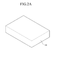
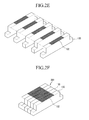
- FIGS. 2A to 2F is diagrams for describing the method for fabricating a microstructure according to the first exemplary embodiment of the present invention.
- the microstructure fabricating method includes exposing photosensitive material 110 at step S101, etching the photosensitive material 110 at step S102, forming a mold at step S103, forming a mold module at step S104, and fabricating a microstructure at step S105.
- photosensitive material 110 made of PMMA is prepared.
- a positive photosensitive material is used.
- a negative photosensitive material may be used as the photosensitive material 110 as well as the positive photosensitive material.
- Negative photosensitive material such as SU-8 stays in liquid. Accordingly, a substrate can be coated with negative photosensitive material at a predetermined thickness by performing spin coating. Then, soft baking is performed to solidify the negative photosensitive material coated on the substrate and to retain the solid state thereof.
- a X-ray mask 120 is disposed on the photosensitive material 110 and an x-ray exposure process is performed by radiating x-rays to the photosensitive material 110 at step S101.
- the X-ray mask 120 includes an absorption part 120b for absorbing X-rays 150, and a penetration part 120b for not absorbing the X-rays.
- the absorption part 120b may be made of gold (Au) that absorbs the X-rays 150 very well and the penetration part 120a may be made of various materials that do not absorb the X-rays 150.
- a predetermined pattern 125 is formed at the X-ray mask 120.
- the predetermined pattern corresponds to a shape of a side of a microstructure.
- the side of the microstructure may be a side that crosses and forms a corner with a top side of the microstructure, where a micro-pattern is formed on the top side of the microstructure.
- a microstructure has four sides.
- the predetermined pattern in the X-ray mask 120 has a shape corresponding to that of a side of the microstructure where micro-patterns are continuously formed. In the present exemplary embodiment, the predetermined pattern has a shape identical to that of the penetration part 120a.
- the X-ray mask 120 is disposed to face a predetermined side of the photosensitive material 110 and the X-rays 150 is radiated toward the X-ray mask 120.
- DXRL Deep X-ray Lithography
- the DXRL has merits of high penetration depth and easy thickness control.
- a microstructure having high aspect ratio can be fabricated through a DXRL process using high energy X-rays.
- the DXRL process using high energy X-rays can be used to fabricate a vertical microstructure because of high collimation of the X-rays. Because it is possible to fabricate a microstructure with superior surface roughness, the DXRL process is used in the present exemplary embodiment.
- a pattern groove 115 having a micro-pattern 115a is formed by etching the photosensitive material 110 as shown in FIG. 2C .
- a positive photosensitive material is exposed at X-rays and a radiated part of the positive photosensitive material is etched.
- the present invention is not limited thereto.
- the present exemplary embodiment can be applied to negative photosensitive material.
- the micro-pattern 115a extends in a depth direction of the pattern groove 115 because the pattern is formed in the X ray mask 120 corresponding to a side of the microstructure.
- the top side of the micro-pattern 115a is formed to be sloped. In order to easily form a 3-D pattern having irregular height of the top side of the micro-pattern 115, the side exposure method is applied.
- a mold 130 is formed by filling the pattern groove 115 with metal as shown in FIG. 2D .
- the mold 130 is made of nickel or nickel alloy. Since the nickel and nickel alloy have excellent mechanical strength, the nickel and nickel alloy are proper metal for fabricating a mold for mass production of a microstructure.
- An electro forming may be applied to fabricate the mold 130.
- a depth of the pattern groove 115 is about 2mm. The pattern groove 115 may be easily filled with nickel using the electro forming.
- the mold 130 having a micro-pattern 132 is separated from the photosensitive material 110.
- a plurality of molds 130 are manufactured using the same method described above. Then, the plurality of molds 130 are arranged as shown in FIG. 2E .
- the micro-pattern 132 is formed at a top side of the mold 130.
- a side shape of the mold 130 corresponds to the pattern formed in the X-ray mask 120.
- a mold module 200 is formed by combining the plurality of molds 130.
- the mold module 200 includes a lengthy-extended micro-pattern.
- the lengthy-extended micro-pattern is formed by stacking the plurality of molds.
- the mold module 200 having the lengthy-extended micro-pattern can be formed even using the side exposure method. That is, the mold module 200 is formed by stacking the plurality of molds in a length direction of the micro-pattern.
- a microstructure 140 having a micro-pattern 145 is fabricated through an injection molding process or a hot embossing process as shown in FIG. 2G .
- the micro structure may be made of metal or polymer.
- a 3-D micro-pattern having an irregular height of a top side can be fabricated according to the present exemplary embodiment.
- FIG. 3A is a picture of a X-ray mask fabricated according to the first exemplary embodiment of the present invention
- FIG. 3B is a picture showing a pattern groove formed using the X-ray mask of FIG. 3A .
- a X-ray mask includes a penetration part for passing X-rays through the X-ray mask and an absorption part for not passing X-rays through the X-ray mask.
- a pattern groove is formed by performing exposure and etching after disposing the X-ray mask.
- the pattern groove has a depth of about 2mm.
- a mold is formed by filling the pattern groove using an electro forming process.
- FIGS. 4A and 4B are pictures showing a mold module produced according to the first exemplary embodiment of the present invention.
- FIG. 4A illustrates a mold module having a micro-pattern formed in a semicircle pillar shape.
- a diameter of the semicircle pillar shaped pattern is about 200 ⁇ m.
- FIG. 4B illustrates a mold module having a micro-pattern formed in an equilateral triangle prism shape.
- a length of one side of the micro-pattern is about 300 ⁇ m.
- FIG. 5 is a perspective view of a mold module manufactured according to the second exemplary embodiment of the present invention.
- a mold module 300 according to the present exemplary embodiment includes a plurality of molds 310, 320, and 330.
- the molds 321, 320, and 330 include micro-patterns 312, 322, and 332, respectively.
- the micro-patterns 312, 322, and 332 are different from each other in shape.
- the mold module 300 according to the present exemplary embodiment includes a first mold 310, a second mold 320, and a third mold 330.
- the first mold 310 has a rectangular parallelepiped shape micro-pattern 312.
- the second mold 320 and the third mold 330 have triangle shape micro-patterns 322 and 332.
- the micro-pattern 322 of the second mold 320 has a height higher than that of the micro-pattern 332 of the third mold 330.
- a plurality of X-ray masks and photosensitive material are prepared to form molds having different shapes in order to form the mold module 300 having the micro-patterns 312, 322, and 332 having different shapes.
- Such a mold module can be formed by combining molds having different shaped micro-patterns. Accordingly, a microstructure having various micro-patterns can be manufactured according to the present exemplary embodiment.
- FIG. 6A is a picture that shows a mold core formed using a mold module manufactured according to the second exemplary embodiment of the present invention
- FIG. 6B is a picture that illustrates a polymer microstructure manufactured using the mold core of FIG. 6A .
- micro-patterns formed on a mold core according to the present exemplary embodiment are gradually reduced in size. That is, such a microstructure can be fabricated using a mold module formed by combining molds micro-patterns different in size.
- FIGS. 7A and 7B are pictures that illustrate a microstructure manufactured according to the second exemplary embodiment of the present invention.
- a first micro-pattern 410 has an equilateral triangle shape and a length of one side is about 500 ⁇ m.
- a second micro-pattern 420 has an equilateral triangle shape and a length of one side is about 450 ⁇ m.
- a third micro-pattern 430 has an equilateral triangle shape and a length of one side is about 400 ⁇ m.
- a fourth micro-pattern 440 has an equilateral triangle shape and a length of one side is about 350 ⁇ m.
- a fifth micro-pattern 450 also has an equilateral triangle shape and a length of one side is about 300 ⁇ m.
- a sixth micro-pattern 460 has an equilateral triangle shape and a length of one side is about 250 ⁇ m.
- a first micro-pattern 510 has an equilateral triangle shape and a length of one side is about 500 ⁇ m.
- a second micro-pattern 520 has a semicircular pillar shape and a diameter thereof is about 500 ⁇ m.
- a third micro-pattern 530 has an equilateral triangle shape and a length of one side is about 400 ⁇ m.
- a fourth micro-pattern 540 has a semicircular pillar shape and a diameter thereof is about 400 ⁇ m.
- Microstructures having various shapes can be fabricated by combining molds having various micro-patterns as shown above.
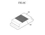
- FIGS. 8A to 8C are diagrams that illustrate a method for fabricating a microstructure according to the third exemplary embodiment of the present invention.
- the microstructure fabricating method according to the third exemplary embodiment includes exposing a photosensitive material and etching the exposed photosensitive material, which are identical to those of the first exemplary embodiment. Accordingly, the detailed descriptions thereof are omitted herein.
- the microstructure fabricating method includes exposing a photosensitive material, etching the photosensitive material, forming a module by stacking photosensitive material layers, forming a mold, and forming a microstructure.
- a photosensitive material 110 is exposed and etched to form a pattern groove 115 having a micro-pattern 115a in the photosensitive material 110.
- the pattern groove 115 penetrates the photosensitive material 110.
- the pattern groove 115 includes the micro-pattern 115a.
- a photosensitive material module 160 is formed by stacking photosensitive material layers 110 each having a pattern groove 115.
- a protrusion 117 is formed at a side of the photosensitive material layer 110.
- the protrusion 117 is protruded upwardly. Due to the protrusion 117, an upper photosensitive material layer can be properly positioned and stacked on a lower photosensitive material layer.
- the protrusion 117 may be formed at diagonal corners of the photosensitive material layer 110.
- the protrusion 117 has a shape bended along an edge of a corner.
- the protrusion 117 may be protruded upwardly from a top side or downwardly from a bottom side of the photosensitive material layer.
- a mold 600 is formed by filling the pattern groove 115 with metal using an electro forming process as shown in FIG. 8B .
- the mold 600 is separated from the photosensitive material module as shown in FIG. 8C .
- the mold 600 includes a pattern 620 having a lengthy-extended pattern 620.
- the mold having a 3-D pattern with irregular height can be easily fabricated using the photosensitive material module 160 formed by stacking the photosensitive material layers 110 according to the present exemplary embodiment. Furthermore, a microstructure having a wide 3-D micro-pattern can be easily fabricated using the mold 600 according to the present exemplary embodiment.
Landscapes
- Physics & Mathematics (AREA)
- General Physics & Mathematics (AREA)
- Engineering & Computer Science (AREA)
- Manufacturing & Machinery (AREA)
- Microelectronics & Electronic Packaging (AREA)
- Health & Medical Sciences (AREA)
- Toxicology (AREA)
- Exposure And Positioning Against Photoresist Photosensitive Materials (AREA)
- Exposure Of Semiconductors, Excluding Electron Or Ion Beam Exposure (AREA)
- Micromachines (AREA)
Abstract
Description
- The present invention relates to a microstructure fabricating method and, more particularly, to a microstructure fabricating method using an x-ray exposure scheme.
- LIGA is a fabrication technology used to create a plastic microstructure using high energy x-rays generated by a synchrotron. LIGA was developed in the early 1980s at Germany. Many studies have been made for advancing LIGA and applications thereof. LIGA is a German acronym for Lithographie, Galvanoformung, and Abformung. That is, LIGA includes a Lithographie process for fabricating a plastic microstructure through X-ray exposure, a Galvanoformung process for forming a mold insert using electro forming, and an Abformung process for forming a microstructure using the mold insert. LIGA was developed for mass production with high productivity, not designed for one time production of a microstructure.
- A micro-electro-mechanical system (MEMS) technology uses an ultraviolet rays (UV) exposure scheme to fabricate a microstructure. Unlike the conventional MEMS technology, LIGA uses high energy X-rays to fabricate a microstructure. Due to the high energy X-rays, a microstructure having a high aspect ratio can be fabricated using LIGA. Furthermore, a microstructure fabricated by LIGA has excellent surface quality. LIGA has been used to produce micro components for optical communication, such as an optical waveguide and an optical connector, precise mechanical parts such as micro motor, and a core part for a heat exchanger and a micro reactor.
- In early development stage, a Deep X-ray Lithography (DXRL) process using high energy x-rays was mainly used. Henceforth, a UV-LIGA process using a UV exposure scheme was introduced and used more as a micro-electro-mechanical system (MEMS) technology has been advanced.
- In LIGA, a microstructure having the same shape of a final product is formed at first through an exposure process. Using the formed microstructure as a mother structure, a mold or a mold insert is formed by performing an electro forming process.
- The final product having the same shape of the initially produced microstructure can be mass-produced through a molding process using the mold.
- In order to mass-produce various microstructures through LIGA, It is necessary to precisely produce a mold or a mold insert. Furthermore, the mold must have a high dimensional accuracy and required mechanical properties as well as a shape of final product. Such requirements must be satisfied in order to stably mass-produce final products.
- Recently, various microstructure fabricating technologies have been used to produce molds or mold inserts for mass-productions of various microstructures. A mold may be produced using a precision machining process or a laser process that directly processes mold material to form a mold. However, the precision machining process or the laser process has drawbacks such as low dimensional accuracy and long production time. Due to such drawbacks, an exposure process in a semiconductor process has been generally used. A microstructure is produced through an exposure process, and a metal mold or a metal mold insert is then produced by performing an electro forming process on the fabricated microstructure.
- As the MEMS technology has been advanced, various exposure processes have been introduced. Such exposure process has merits of process automation, high dimensional accuracy, and high yield. A microstructure fabricated through typical exposure process has a planar shape. It is because a direction of radiating light is vertical to a substrate and photosensitive material coated on the substrate. Accordingly, it is difficult to produce a microstructure having various 3-D shapes of different heights of inclined planes in case of the vertical exposure scheme.
- A microstructure having a constant slope can be manufactured through a method for radiating light using an inclined exposure scheme. However, only limited microstructures can be produced using the inclined exposure scheme. Further, it is very difficult to manufacture a mask used for the inclined exposure scheme, and complicated equipment is additionally required to use the inclined exposure scheme. Accordingly, the inclined exposure scheme has been used only for specific cases.
- Moreover, the inclined exposure scheme also has limitation in depth exposed by X-rays. Accordingly, it is impossible to produce a microstructure having a complicated shaped in a width direction thereof using the inclined exposure scheme.
- The above information disclosed in this Background section is only for enhancement of understanding of the background of the invention and therefore it may contain information that does not form the prior art that is already known in this country to a person of ordinary skill in the art.
- The present invention has been made in an effort to provide a microstructure fabricating method having advantages of easily fabricating microstructures having various shapes.
- An exemplary embodiment of the present invention provides a method for fabricating a microstructure including disposing an X-ray mask on photosensitive material and exposing the photosensitive material by radiating X-rays to the photosensitive material using a side exposure scheme, etching the exposed photosensitive material, forming a mold having a micro-pattern by filing the etched photosensitive material with metal, forming a mold module by combining a plurality of molds, and forming a microstructure using the mold module.
- In the exposing the photosensitive material, a Deep X-Ray Lithography (DXRL) process may be performed to expose the photosensitive material. The plurality of molds may have micro-patterns different in shape. The forming a mold may include electro forming. In the forming a mold, metal may be one of nickel and nickel alloy.
- The micro-pattern may be a three dimensional (3-D) micro-pattern having an irregular height of a top side. The X-ray mask may have a pattern shape corresponding to a shape of a side of the microstructure. The plurality of molds may be arranged and stacked in a length direction of the micro-pattern.
- Another exemplary embodiment of the present invention provides a method for fabricating a microstructure, including disposing an X-ray mask on photosensitive material and exposing the photosensitive material by radiating X-rays using a side exposure method, etching the exposed photosensitive material, forming a photosensitive module by arranging and stacking the etched photosensitive materials, forming a mold having a micro-pattern by filling the photosensitive module with metal, and Deleted Texts forming a microstructure using the mold.
- In the exposing the photosensitive material, a Deep X-Ray Lithography (DXRL) process may be performed to expose the photosensitive material. Micro-patterns may be formed at the etched photosensitive materials, and the micro-patterns may be different from each other in shape.
- The photosensitive materials may be arranged and stacked in a length direction of the micro-pattern. The forming a mold may include electro forming.
- In the forming a mold, metal may be one of nickel and nickel alloy. The micro-pattern may be a three dimensional (3-D) micro-pattern having an irregular height of a top side.
- The X-ray mask may have a pattern having a shape corresponding to a shape of a side of the microstructure. A protrusion may be formed at a corner of the photosensitive material to support neighbor photosensitive material, and the protrusion is protruded upwardly from a top side of the photosensitive material or downwardly from a bottom side of the photosensitive material.
- According to the present exemplary embodiment, a microstructure having a 3-D shaped micro-pattern can be easily fabricated. Further, a length of a micro-pattern can be extended using a side exposure scheme and a mold module.
-
-
FIG. 1 is a flowchart that illustrates a method for fabricating a microstructure according to the first exemplary embodiment of the present invention. -
FIGS. 2A to 2F is diagrams for describing the method for fabricating a microstructure according to the first exemplary embodiment of the present invention. -
FIG. 3A is a picture of a X-ray mask fabricated according to the first exemplary embodiment of the present invention, andFIG. 3B is a picture showing a pattern groove formed using the X-ray mask ofFIG. 3A . -
FIGS. 4A and 4B are pictures showing a mold module produced according to the first exemplary embodiment of the present invention. -
FIG. 5 is a perspective view of a mold module manufactured according to the second exemplary embodiment of the present invention. -
FIG. 6A is a picture that shows a mold core formed using a mold module manufactured according to the second exemplary embodiment of the present invention, andFIG. 6B is a picture that illustrates a polymer microstructure manufactured using the mold core ofFIG. 6A . -
FIGS. 7A and 7B are pictures that illustrate a microstructure manufactured according to the second exemplary embodiment of the present invention. -
FIGS. 8A to 8C are diagrams that illustrate a method for fabricating a microstructure according to the third exemplary embodiment of the present invention. - In the present invention, "side exposure" means a process that expose a predetermined object by radiating light to a side of the predetermined object, which crosses another side having a micro-pattern. Further, "micro-pattern" or "microstructure" means a pattern or a structure having a nano size pitch or a micro size pitch.
- In the following detailed description, only certain exemplary embodiments of the present invention have been shown and described, simply by way of illustration. As those skilled in the art would realize, the described embodiments may be modified in various different ways, all without departing from the spirit or scope of the present invention. The drawings and description are to be regarded as illustrative in nature and not restrictive. Like reference numerals designate like elements throughout the specification.
-
FIG. 1 is a flowchart that illustrates a method for fabricating a microstructure according to the first exemplary embodiment of the present invention.FIGS. 2A to 2F is diagrams for describing the method for fabricating a microstructure according to the first exemplary embodiment of the present invention. - Referring to
FIG. 1 , the microstructure fabricating method according to the present exemplary embodiment includes exposingphotosensitive material 110 at step S101, etching thephotosensitive material 110 at step S102, forming a mold at step S103, forming a mold module at step S104, and fabricating a microstructure at step S105. - As shown in
FIG. 2A ,photosensitive material 110 made of PMMA is prepared. In the present exemplary embodiment, a positive photosensitive material is used. A negative photosensitive material, however, may be used as thephotosensitive material 110 as well as the positive photosensitive material. - Negative photosensitive material such as SU-8 stays in liquid. Accordingly, a substrate can be coated with negative photosensitive material at a predetermined thickness by performing spin coating. Then, soft baking is performed to solidify the negative photosensitive material coated on the substrate and to retain the solid state thereof.
- As shown in
FIG. 2B , aX-ray mask 120 is disposed on thephotosensitive material 110 and an x-ray exposure process is performed by radiating x-rays to thephotosensitive material 110 at step S101. - The
X-ray mask 120 includes anabsorption part 120b for absorbingX-rays 150, and apenetration part 120b for not absorbing the X-rays. Theabsorption part 120b may be made of gold (Au) that absorbs theX-rays 150 very well and thepenetration part 120a may be made of various materials that do not absorb theX-rays 150. - A
predetermined pattern 125 is formed at theX-ray mask 120. The predetermined pattern corresponds to a shape of a side of a microstructure. The side of the microstructure may be a side that crosses and forms a corner with a top side of the microstructure, where a micro-pattern is formed on the top side of the microstructure. When a microstructure has a quadrangle-shaped top side, a microstructure has four sides. The predetermined pattern in theX-ray mask 120 has a shape corresponding to that of a side of the microstructure where micro-patterns are continuously formed. In the present exemplary embodiment, the predetermined pattern has a shape identical to that of thepenetration part 120a. - The
X-ray mask 120 is disposed to face a predetermined side of thephotosensitive material 110 and theX-rays 150 is radiated toward theX-ray mask 120. - In case of applying such a side exposure scheme, it is advantageous to use a Deep X-ray Lithography (DXRL). The DXRL has merits of high penetration depth and easy thickness control. Particularly, a microstructure having high aspect ratio can be fabricated through a DXRL process using high energy X-rays. The DXRL process using high energy X-rays can be used to fabricate a vertical microstructure because of high collimation of the X-rays. Because it is possible to fabricate a microstructure with superior surface roughness, the DXRL process is used in the present exemplary embodiment.
- After radiating the
X-ray 150, apattern groove 115 having a micro-pattern 115a is formed by etching thephotosensitive material 110 as shown inFIG. 2C . In the present exemplary embodiment, a positive photosensitive material is exposed at X-rays and a radiated part of the positive photosensitive material is etched. However, the present invention is not limited thereto. The present exemplary embodiment can be applied to negative photosensitive material. - The micro-pattern 115a extends in a depth direction of the
pattern groove 115 because the pattern is formed in theX ray mask 120 corresponding to a side of the microstructure. The top side of the micro-pattern 115a is formed to be sloped. In order to easily form a 3-D pattern having irregular height of the top side of the micro-pattern 115, the side exposure method is applied. - After forming the
pattern groove 115, amold 130 is formed by filling the pattern groove 115 with metal as shown inFIG. 2D . Themold 130 is made of nickel or nickel alloy. Since the nickel and nickel alloy have excellent mechanical strength, the nickel and nickel alloy are proper metal for fabricating a mold for mass production of a microstructure. An electro forming may be applied to fabricate themold 130. A depth of thepattern groove 115 is about 2mm. Thepattern groove 115 may be easily filled with nickel using the electro forming. - As shown in
FIG. 2E , themold 130 having a micro-pattern 132 is separated from thephotosensitive material 110. A plurality ofmolds 130 are manufactured using the same method described above. Then, the plurality ofmolds 130 are arranged as shown inFIG. 2E . - As shown, the micro-pattern 132 is formed at a top side of the
mold 130. A side shape of themold 130 corresponds to the pattern formed in theX-ray mask 120. - As shown in
FIG. 2F , amold module 200 is formed by combining the plurality ofmolds 130. Themold module 200 includes a lengthy-extended micro-pattern. - Due to penetration limitation of X-ray, it is difficult to form a lengthy-extended pattern using the side exposure method. In the exemplary embodiment, the lengthy-extended micro-pattern is formed by stacking the plurality of molds. In this method, the
mold module 200 having the lengthy-extended micro-pattern can be formed even using the side exposure method. That is, themold module 200 is formed by stacking the plurality of molds in a length direction of the micro-pattern. - After forming the mold module, a
microstructure 140 having a micro-pattern 145 is fabricated through an injection molding process or a hot embossing process as shown inFIG. 2G . The micro structure may be made of metal or polymer. - As described a 3-D micro-pattern having an irregular height of a top side can be fabricated according to the present exemplary embodiment.
-
FIG. 3A is a picture of a X-ray mask fabricated according to the first exemplary embodiment of the present invention, andFIG. 3B is a picture showing a pattern groove formed using the X-ray mask ofFIG. 3A . - As shown in
FIG. 3A , a X-ray mask includes a penetration part for passing X-rays through the X-ray mask and an absorption part for not passing X-rays through the X-ray mask. - As shown in
FIG. 3B , a pattern groove is formed by performing exposure and etching after disposing the X-ray mask. Here, the pattern groove has a depth of about 2mm. A mold is formed by filling the pattern groove using an electro forming process. -
FIGS. 4A and 4B are pictures showing a mold module produced according to the first exemplary embodiment of the present invention. -
FIG. 4A illustrates a mold module having a micro-pattern formed in a semicircle pillar shape. Here, a diameter of the semicircle pillar shaped pattern is about 200µm.FIG. 4B illustrates a mold module having a micro-pattern formed in an equilateral triangle prism shape. Here, a length of one side of the micro-pattern is about 300µm. -
FIG. 5 is a perspective view of a mold module manufactured according to the second exemplary embodiment of the present invention. - A
mold module 300 according to the present exemplary embodiment includes a plurality ofmolds molds micro-patterns micro-patterns mold module 300 according to the present exemplary embodiment includes afirst mold 310, asecond mold 320, and athird mold 330. Thefirst mold 310 has a rectangularparallelepiped shape micro-pattern 312. Thesecond mold 320 and thethird mold 330 have triangle shape micro-patterns 322 and 332. Further, the micro-pattern 322 of thesecond mold 320 has a height higher than that of the micro-pattern 332 of thethird mold 330. - In the present exemplary embodiment, a plurality of X-ray masks and photosensitive material are prepared to form molds having different shapes in order to form the
mold module 300 having themicro-patterns - Such a mold module can be formed by combining molds having different shaped micro-patterns. Accordingly, a microstructure having various micro-patterns can be manufactured according to the present exemplary embodiment.
-
FIG. 6A is a picture that shows a mold core formed using a mold module manufactured according to the second exemplary embodiment of the present invention, andFIG. 6B is a picture that illustrates a polymer microstructure manufactured using the mold core ofFIG. 6A . - Referring to
FIGS. 6A and 6B , micro-patterns formed on a mold core according to the present exemplary embodiment are gradually reduced in size. That is, such a microstructure can be fabricated using a mold module formed by combining molds micro-patterns different in size. -
FIGS. 7A and 7B are pictures that illustrate a microstructure manufactured according to the second exemplary embodiment of the present invention. - Referring to
FIG. 7A , afirst micro-pattern 410 has an equilateral triangle shape and a length of one side is about 500µm. Asecond micro-pattern 420 has an equilateral triangle shape and a length of one side is about 450µm. Athird micro-pattern 430 has an equilateral triangle shape and a length of one side is about 400µm. Afourth micro-pattern 440 has an equilateral triangle shape and a length of one side is about 350µm. Afifth micro-pattern 450 also has an equilateral triangle shape and a length of one side is about 300µm. Asixth micro-pattern 460 has an equilateral triangle shape and a length of one side is about 250µm. - Referring to
FIG. 7B , afirst micro-pattern 510 has an equilateral triangle shape and a length of one side is about 500µm. Asecond micro-pattern 520 has a semicircular pillar shape and a diameter thereof is about 500µm. Athird micro-pattern 530 has an equilateral triangle shape and a length of one side is about 400µm. Afourth micro-pattern 540 has a semicircular pillar shape and a diameter thereof is about 400µm. - Microstructures having various shapes can be fabricated by combining molds having various micro-patterns as shown above.
-
FIGS. 8A to 8C are diagrams that illustrate a method for fabricating a microstructure according to the third exemplary embodiment of the present invention. - The microstructure fabricating method according to the third exemplary embodiment includes exposing a photosensitive material and etching the exposed photosensitive material, which are identical to those of the first exemplary embodiment. Accordingly, the detailed descriptions thereof are omitted herein.
- The microstructure fabricating method according to the present exemplary embodiment includes exposing a photosensitive material, etching the photosensitive material, forming a module by stacking photosensitive material layers, forming a mold, and forming a microstructure.
- As shown in
FIG. 8A , aphotosensitive material 110 is exposed and etched to form apattern groove 115 having a micro-pattern 115a in thephotosensitive material 110. Thepattern groove 115 penetrates thephotosensitive material 110. Thepattern groove 115 includes the micro-pattern 115a. Aphotosensitive material module 160 is formed by stackingphotosensitive material layers 110 each having apattern groove 115. - In order to properly stack the
photosensitive material layers 110 at a predetermined position, aprotrusion 117 is formed at a side of thephotosensitive material layer 110. Theprotrusion 117 is protruded upwardly. Due to theprotrusion 117, an upper photosensitive material layer can be properly positioned and stacked on a lower photosensitive material layer. Theprotrusion 117 may be formed at diagonal corners of thephotosensitive material layer 110. Theprotrusion 117 has a shape bended along an edge of a corner. Theprotrusion 117 may be protruded upwardly from a top side or downwardly from a bottom side of the photosensitive material layer. - After stacking the
photosensitive material 110, amold 600 is formed by filling the pattern groove 115 with metal using an electro forming process as shown inFIG. 8B . Themold 600 is separated from the photosensitive material module as shown inFIG. 8C . Themold 600 includes apattern 620 having a lengthy-extended pattern 620. - As described above, the mold having a 3-D pattern with irregular height can be easily fabricated using the
photosensitive material module 160 formed by stacking thephotosensitive material layers 110 according to the present exemplary embodiment. Furthermore, a microstructure having a wide 3-D micro-pattern can be easily fabricated using themold 600 according to the present exemplary embodiment. - While this invention has been described in connection with what is presently considered to be practical exemplary embodiments, it is to be understood that the invention is not limited to the disclosed embodiments, but, on the contrary, is intended to cover various modifications and equivalent arrangements included within the spirit and scope of the appended claims.
Claims (17)
- A method for fabricating a microstructure, comprising:disposing an X-ray mask on photosensitive material and exposing the photosensitive material by radiating X-rays to the photosensitive material using a side exposure scheme;etching the exposed photosensitive material;forming a mold having a micro-pattern by filing the etched photosensitive material with metal;forming a mold module by combining a plurality of molds; andforming a microstructure using the mold module;
- The method of claim 1, wherein in the exposing the photosensitive material, a Deep X-Ray Lithography (DXRL) process is performed to expose the photosensitive material.
- The method of claim 1, wherein the plurality of molds have micro-patterns different in shape.
- The method of claim 1, wherein the forming a mold includes electro forming.
- The method of claim 4, wherein in the forming a mold, metal is one of nickel and nickel alloy.
- The method of claim 1, wherein the micro-pattern is a three dimensional (3-D) micro-pattern having an irregular height of a top side.
- The method of claim 1, wherein:the X-ray mask has a pattern shape corresponding to a shape of a side of the microstructure.
- The method of claim 1, wherein the plurality of molds is arranged and stacked in a length direction of the micro-pattern.
- A method for fabricating a microstructure, comprising;
disposing an X-ray mask on photosensitive material and exposing the photosensitive material by radiating X-rays using a side exposure method;
etching the exposed photosensitive material;
forming a photosensitive module by arranging and stacking the etched photosensitive materials;
forming a mold having a micro-pattern by filling the photosensitive module with metal; and
forming a microstructure using the mold. - The method of claim 9, wherein in the exposing the photosensitive material, a Deep X-Ray Lithography (DXRL) process is performed to expose the photosensitive material.
- The method of claim 9, wherein:micro-patterns are formed at the etched photosensitive materials, and the micro-patterns are different from each other in shape.
- The method of claim 11, wherein:the photosensitive materials are arranged and stacked in a length direction of the micro-pattern.
- The method of claim 9, wherein the forming a mold includes electro forming.
- The method of claim 13, wherein in the forming a mold, metal is one of nickel and nickel alloy.
- The method of claim 9, wherein the micro-pattern is a three dimensional (3-D) micro-pattern having an irregular height of a top side.
- The method of claim 9, wherein the X-ray mask has a pattern having a shape corresponding to a shape of a side of the microstructure.
- The method of claim 9, wherein a protrusion is formed at a corner of the photosensitive material to support neighbor photosensitive material, and the protrusion is protruded upwardly from a top side of the photosensitive material or downwardly from a bottom side of the photosensitive material.
Applications Claiming Priority (2)
| Application Number | Priority Date | Filing Date | Title |
|---|---|---|---|
| KR1020080110582A KR101020187B1 (en) | 2008-11-07 | 2008-11-07 | Microstructure manufacturing method using X-ray exposure |
| PCT/KR2009/006385 WO2010053277A2 (en) | 2008-11-07 | 2009-11-02 | Method for manufacturing micro structure using x-ray exposure |
Publications (2)
| Publication Number | Publication Date |
|---|---|
| EP2355136A2 true EP2355136A2 (en) | 2011-08-10 |
| EP2355136A4 EP2355136A4 (en) | 2013-01-23 |
Family
ID=42153377
Family Applications (1)
| Application Number | Title | Priority Date | Filing Date |
|---|---|---|---|
| EP20090824960 Withdrawn EP2355136A4 (en) | 2008-11-07 | 2009-11-02 | METHOD FOR MANUFACTURING MICRO STRUCTURE BY X-RAY EXPOSURE |
Country Status (5)
| Country | Link |
|---|---|
| US (1) | US9217927B2 (en) |
| EP (1) | EP2355136A4 (en) |
| KR (1) | KR101020187B1 (en) |
| CN (1) | CN102210008A (en) |
| WO (1) | WO2010053277A2 (en) |
Families Citing this family (1)
| Publication number | Priority date | Publication date | Assignee | Title |
|---|---|---|---|---|
| CN113714393B (en) * | 2021-09-03 | 2024-02-02 | 广东安居宝数码科技股份有限公司 | Edge covering mold, using method and edge covering frame |
Family Cites Families (3)
| Publication number | Priority date | Publication date | Assignee | Title |
|---|---|---|---|---|
| KR100367960B1 (en) * | 2000-09-25 | 2003-01-14 | 김병수 | A method of manufacturing mold for barrier ribs replication of PDP rear panel by a new forming technology and fabrication |
| KR100451433B1 (en) | 2001-10-12 | 2004-10-06 | 학교법인 포항공과대학교 | Method for manufacturing triangular riblet and the mold by using liga process |
| JP2004273794A (en) | 2003-03-10 | 2004-09-30 | Mitsubishi Electric Corp | Method of manufacturing X-ray mask and method of manufacturing semiconductor device using X-ray mask manufactured thereby |
-
2008
- 2008-11-07 KR KR1020080110582A patent/KR101020187B1/en not_active Expired - Fee Related
-
2009
- 2009-11-02 US US13/128,016 patent/US9217927B2/en not_active Expired - Fee Related
- 2009-11-02 CN CN2009801446619A patent/CN102210008A/en active Pending
- 2009-11-02 WO PCT/KR2009/006385 patent/WO2010053277A2/en not_active Ceased
- 2009-11-02 EP EP20090824960 patent/EP2355136A4/en not_active Withdrawn
Non-Patent Citations (4)
| Title |
|---|
| HUI YOU ET AL: "Deep x-ray exposure system with multistage for 3-D microfabrication", MICROMECHATRONICS AND HUMAN SCIENCE, 2000. MHS 2000. PROCEEDINGS OF 20 00 INTERNATIONAL SYMPOSIUM ON OCTOBER 22-25, 2000, PISCATAWAY, NJ, USA,IEEE, 22 October 2000 (2000-10-22), pages 53-58, XP010531638, ISBN: 978-0-7803-6498-1 * |
| PERENNES F ET AL: "Sharp beveled tip hollow microneedle arrays fabricated by LIGA and 3D soft lithography with polyvinyl alcohol", JOURNAL OF MICROMECHANICS AND MICROENGINEERING IOP PUBLISHING UK, vol. 16, no. 3, 25 January 2006 (2006-01-25), pages 473-479, XP002688468, ISSN: 0960-1317 * |
| SCHULZE J ET AL: "Parallel optical interconnection using self-adjusting microlenses on injection-molded ferrules made by LIGA technique", PROCEEDINGS OF THE SPIE - THE INTERNATIONAL SOCIETY FOR OPTICAL ENGINEERING, vol. 3737, 1999, pages 562-571, XP002688469, SPIE-INT. SOC. OPT. ENG. USA ISSN: 0277-786X, DOI: 10.1117/12.360052 * |
| See also references of WO2010053277A2 * |
Also Published As
| Publication number | Publication date |
|---|---|
| CN102210008A (en) | 2011-10-05 |
| US9217927B2 (en) | 2015-12-22 |
| KR101020187B1 (en) | 2011-03-07 |
| KR20100051418A (en) | 2010-05-17 |
| EP2355136A4 (en) | 2013-01-23 |
| WO2010053277A2 (en) | 2010-05-14 |
| US20110254195A1 (en) | 2011-10-20 |
| WO2010053277A3 (en) | 2010-08-05 |
Similar Documents
| Publication | Publication Date | Title |
|---|---|---|
| Malek et al. | Applications of LIGA technology to precision manufacturing of high-aspect-ratio micro-components and-systems: a review | |
| JP5670198B2 (en) | Optical element and method for manufacturing wafer scale assembly | |
| US20100183760A1 (en) | Manufacturing micro-structured elements | |
| US6582890B2 (en) | Multiple wavelength photolithography for preparing multilayer microstructures | |
| WO2015093945A1 (en) | Method of fabricating a wafer level optical lens assembly | |
| JP2012035578A (en) | Mold for nanoimprinting | |
| KR101114469B1 (en) | Fabricating method of two-dimensional polymeric optical waveguide | |
| US9217927B2 (en) | Method for manufacturing micro structure using X-ray exposure | |
| KR101828636B1 (en) | Method and device for producing a lens wafer | |
| JPWO2012102249A1 (en) | Mold, wafer lens and optical lens manufacturing method | |
| US20100019408A1 (en) | Minute flow path structure body and die | |
| KR20140076947A (en) | Mold structure and method of imprint lithography using the same | |
| KR100911908B1 (en) | Manufacturing method of mold and molded article obtained by it | |
| JP5753696B2 (en) | LENS MOLD MOLD MANUFACTURING METHOD AND LENS MANUFACTURING METHOD | |
| Stöhr et al. | Injection molded polymeric hard X-ray lenses | |
| Rodríguez et al. | 3D Micro‐Printing Goes Macro: Tailor‐made materials enable pioneering developments and applications | |
| KR101132748B1 (en) | Micro mold system, manufacturing method thereof, and manufacturing method of micro-precision parts | |
| KR101232838B1 (en) | Roll-type micromold system and fabrication method of the same | |
| US12276813B2 (en) | Method of manufacturing a plurality of optical elements and product thereof | |
| Stankevich et al. | Deep X-ray Lithography: A Brief Review | |
| KR100983043B1 (en) | Micro Lens Master and Micro Lens Manufacturing Method | |
| KR20100081417A (en) | Separated micromold for a fabrication of microstructures by liga process and method for manufacturing the same | |
| KR20250108885A (en) | Methods for manufacturing precision molds and ultra-precision injection parts | |
| JP2018163942A (en) | Imprint mold and method of manufacturing imprint mold | |
| KR20200121976A (en) | The producing methodology of precise mould and high precise injection products |
Legal Events
| Date | Code | Title | Description |
|---|---|---|---|
| PUAI | Public reference made under article 153(3) epc to a published international application that has entered the european phase |
Free format text: ORIGINAL CODE: 0009012 |
|
| 17P | Request for examination filed |
Effective date: 20110527 |
|
| AK | Designated contracting states |
Kind code of ref document: A2 Designated state(s): AT BE BG CH CY CZ DE DK EE ES FI FR GB GR HR HU IE IS IT LI LT LU LV MC MK MT NL NO PL PT RO SE SI SK SM TR |
|
| DAX | Request for extension of the european patent (deleted) | ||
| RIC1 | Information provided on ipc code assigned before grant |
Ipc: B81C 99/00 20100101ALI20121210BHEP Ipc: G03F 7/00 20060101AFI20121210BHEP Ipc: G03F 7/20 20060101ALI20121210BHEP |
|
| A4 | Supplementary search report drawn up and despatched |
Effective date: 20121221 |
|
| RIC1 | Information provided on ipc code assigned before grant |
Ipc: G03F 7/20 20060101ALI20121214BHEP Ipc: G03F 7/00 20060101AFI20121214BHEP Ipc: B81C 99/00 20100101ALI20121214BHEP |
|
| 17Q | First examination report despatched |
Effective date: 20150504 |
|
| STAA | Information on the status of an ep patent application or granted ep patent |
Free format text: STATUS: THE APPLICATION IS DEEMED TO BE WITHDRAWN |
|
| 18D | Application deemed to be withdrawn |
Effective date: 20150915 |