EP2351962A1 - Surface light source device - Google Patents
Surface light source device Download PDFInfo
- Publication number
- EP2351962A1 EP2351962A1 EP10734887A EP10734887A EP2351962A1 EP 2351962 A1 EP2351962 A1 EP 2351962A1 EP 10734887 A EP10734887 A EP 10734887A EP 10734887 A EP10734887 A EP 10734887A EP 2351962 A1 EP2351962 A1 EP 2351962A1
- Authority
- EP
- European Patent Office
- Prior art keywords
- light
- light guide
- guides
- support
- light source
- Prior art date
- Legal status (The legal status is an assumption and is not a legal conclusion. Google has not performed a legal analysis and makes no representation as to the accuracy of the status listed.)
- Withdrawn
Links
- 239000000463 material Substances 0.000 claims abstract description 32
- 238000000149 argon plasma sintering Methods 0.000 claims abstract description 14
- 230000003287 optical effect Effects 0.000 claims description 20
- 239000013013 elastic material Substances 0.000 claims description 4
- 239000004973 liquid crystal related substance Substances 0.000 description 16
- 239000004417 polycarbonate Substances 0.000 description 7
- 206010047571 Visual impairment Diseases 0.000 description 4
- 230000004397 blinking Effects 0.000 description 4
- 238000006073 displacement reaction Methods 0.000 description 4
- 238000005286 illumination Methods 0.000 description 4
- 229920000515 polycarbonate Polymers 0.000 description 4
- 230000000694 effects Effects 0.000 description 3
- 239000000758 substrate Substances 0.000 description 3
- 239000004793 Polystyrene Substances 0.000 description 2
- VYPSYNLAJGMNEJ-UHFFFAOYSA-N Silicium dioxide Chemical compound O=[Si]=O VYPSYNLAJGMNEJ-UHFFFAOYSA-N 0.000 description 2
- 239000013078 crystal Substances 0.000 description 2
- 238000011156 evaluation Methods 0.000 description 2
- 238000004519 manufacturing process Methods 0.000 description 2
- 229920003229 poly(methyl methacrylate) Polymers 0.000 description 2
- 239000004926 polymethyl methacrylate Substances 0.000 description 2
- 230000015556 catabolic process Effects 0.000 description 1
- 238000006731 degradation reaction Methods 0.000 description 1
- 239000000835 fiber Substances 0.000 description 1
- 238000003780 insertion Methods 0.000 description 1
- 230000037431 insertion Effects 0.000 description 1
- 238000000034 method Methods 0.000 description 1
- 229920002223 polystyrene Polymers 0.000 description 1
- 239000000377 silicon dioxide Substances 0.000 description 1
Images






Classifications
-
- G—PHYSICS
- G02—OPTICS
- G02B—OPTICAL ELEMENTS, SYSTEMS OR APPARATUS
- G02B6/00—Light guides; Structural details of arrangements comprising light guides and other optical elements, e.g. couplings
- G02B6/0001—Light guides; Structural details of arrangements comprising light guides and other optical elements, e.g. couplings specially adapted for lighting devices or systems
- G02B6/0011—Light guides; Structural details of arrangements comprising light guides and other optical elements, e.g. couplings specially adapted for lighting devices or systems the light guides being planar or of plate-like form
- G02B6/0075—Arrangements of multiple light guides
- G02B6/0078—Side-by-side arrangements, e.g. for large area displays
-
- G—PHYSICS
- G02—OPTICS
- G02B—OPTICAL ELEMENTS, SYSTEMS OR APPARATUS
- G02B6/00—Light guides; Structural details of arrangements comprising light guides and other optical elements, e.g. couplings
- G02B6/0001—Light guides; Structural details of arrangements comprising light guides and other optical elements, e.g. couplings specially adapted for lighting devices or systems
- G02B6/0011—Light guides; Structural details of arrangements comprising light guides and other optical elements, e.g. couplings specially adapted for lighting devices or systems the light guides being planar or of plate-like form
- G02B6/0081—Mechanical or electrical aspects of the light guide and light source in the lighting device peculiar to the adaptation to planar light guides, e.g. concerning packaging
- G02B6/0086—Positioning aspects
- G02B6/0088—Positioning aspects of the light guide or other optical sheets in the package
-
- G—PHYSICS
- G02—OPTICS
- G02F—OPTICAL DEVICES OR ARRANGEMENTS FOR THE CONTROL OF LIGHT BY MODIFICATION OF THE OPTICAL PROPERTIES OF THE MEDIA OF THE ELEMENTS INVOLVED THEREIN; NON-LINEAR OPTICS; FREQUENCY-CHANGING OF LIGHT; OPTICAL LOGIC ELEMENTS; OPTICAL ANALOGUE/DIGITAL CONVERTERS
- G02F1/00—Devices or arrangements for the control of the intensity, colour, phase, polarisation or direction of light arriving from an independent light source, e.g. switching, gating or modulating; Non-linear optics
- G02F1/01—Devices or arrangements for the control of the intensity, colour, phase, polarisation or direction of light arriving from an independent light source, e.g. switching, gating or modulating; Non-linear optics for the control of the intensity, phase, polarisation or colour
- G02F1/13—Devices or arrangements for the control of the intensity, colour, phase, polarisation or direction of light arriving from an independent light source, e.g. switching, gating or modulating; Non-linear optics for the control of the intensity, phase, polarisation or colour based on liquid crystals, e.g. single liquid crystal display cells
- G02F1/133—Constructional arrangements; Operation of liquid crystal cells; Circuit arrangements
- G02F1/1333—Constructional arrangements; Manufacturing methods
- G02F1/1335—Structural association of cells with optical devices, e.g. polarisers or reflectors
- G02F1/1336—Illuminating devices
- G02F1/133615—Edge-illuminating devices, i.e. illuminating from the side
-
- G—PHYSICS
- G02—OPTICS
- G02B—OPTICAL ELEMENTS, SYSTEMS OR APPARATUS
- G02B6/00—Light guides; Structural details of arrangements comprising light guides and other optical elements, e.g. couplings
- G02B6/0001—Light guides; Structural details of arrangements comprising light guides and other optical elements, e.g. couplings specially adapted for lighting devices or systems
- G02B6/0011—Light guides; Structural details of arrangements comprising light guides and other optical elements, e.g. couplings specially adapted for lighting devices or systems the light guides being planar or of plate-like form
- G02B6/0033—Means for improving the coupling-out of light from the light guide
- G02B6/005—Means for improving the coupling-out of light from the light guide provided by one optical element, or plurality thereof, placed on the light output side of the light guide
- G02B6/0051—Diffusing sheet or layer
Definitions
- the present invention relates to a planar light source device for use as a backlight that includes a side-edge type (also referred to as side-light type) light guide plate through which light from a light source is planarly emitted, for sliming down of a liquid crystal display apparatus, for example.
- a side-edge type also referred to as side-light type
- liquid crystal display apparatuses have used backlights including a side-edge type (also referred to as side-light type) light guide plate through which light from a light source is planarly emitted, for sliming down thereof.
- a side-edge type also referred to as side-light type
- an illumination device is disclosed in Patent Literature 1, for example.
- an illumination device 100 disclosed in Patent literature 1 has: a light guide plate 110 consisting of a plurality of light guides 111 arranged in a row; and a plurality of light sources 101 that is provided for each of the light guides 111 of the light guide plate 110 and irradiate the light guides 111 with light.
- Each of the light sources 101 consists of one red LED (Light Emitting Diode) 101R, two green LEDs 101G, and one blue LED 101B.
- a reflecting sheet 102 is provided under the light guide plate 110.
- gaps 103 are formed between the adjacent light guides 111.
- the gaps 103 are air layers of not less than 0. 1 ⁇ m. With this arrangement, pseudo impulse-type display is realized.
- Patent Literature 2 a light-emitter structure of the same kind is disclosed in Patent Literature 2, for example.
- the gaps 103 are required each in the order of 1 to 2 mm in consideration of thermal expansion and manufacturing tolerances of the light guides 111.
- the support is provided to support the light guides at predetermined intervals.
- the support is made from a material that does not allow light to pass through it (highly reflective PC (polycarbonate), etc.)
- light emitted from the side walls of the light guides is blocked by the support in an area X where the light guides are very close to each other.
- light emitted from the light guides is blocked in an area Y where the support is closer to the diffusing plate than the light guide. This results in lower luminance.
- An object of the present invention is to provide a planar light source device that enables reduction of the occurrence of luminance unevenness caused by a support for supporting light guides, and an electronic apparatus including the planar light source device.
- a planar light source device of the present invention includes: a plurality of light guides being provided such that longer sides thereof are arranged in parallel with each other with a gap therebetween; a plurality of light sources each of which causes light to be directed from at least one of opposite end surfaces of the light guide in the longitudinal direction of the light guide; a plurality of optical path changing sections being provided on a light emission side of the light guide or on a reflecting sheet side opposite the light emission side, to extract light guided inside the light guide; and supports for supporting the light guides at predetermined intervals, the supports being made from a light-transmissive and light-scattering material.
- the supports for supporting the light guides at the predetermined intervals are made from a light-transmissive and light-scattering material, which can prevent the possibility of lower luminance in the gap between the light guides. That is, the support, by virtue of its light-transmissive property, does not block light emitted from side wall surfaces of the light guides. Further, the support, by virtue of its light-scattering property, scatters light emitted from the side wall surfaces, which irradiates the gap between the light guides with light having uniform luminance.
- a planar light source device of the present invention preferably includes: a plurality of light guides being provided such that longer sides thereof are arranged in parallel with each other with a gap therebetween; a plurality of light sources each of which causes light to enter at least one of opposite end surfaces of the light guide in the longitudinal direction of the light guide; a plurality of optical path changing sections being provided on a light emission side of the light guide or on a reflecting sheet side opposite the light emission side, to extract light guided inside the light guide; a diffusing member which diffuses light emitted from the light guides; and supports for supporting the light guides at predetermined intervals, the supports having the same optical properties as the diffusing member.
- Each of the supports has fixing members disposed between the light guides, and the fixing members make one light guide caught therebetween to fix the light guide.
- each of the supports has fixing members disposed between the light guides, and the fixing members make one light guide caught therebetween to fix the light guide.
- the fixing member exists in the gap between the light guides. This ensures the light guides to be supported at predetermined intervals.
- the support has light-transmissive property and light-scattering property. Because of this, even with the existence of the fixing member in the gap between the light guides, light emitted from the side walls of the light guide is not blocked. That is, even with the existence of the fixing member exists in the gap between the light guides, it is possible to curb lower luminance caused by the fixing member.
- the fixing members are preferably made from an elastic material that energizes the light guide to be caught between the fixing members.
- the fixing members are made from an elastic material that energizes the light guide to be caught between the fixing members, which enables the light guide to be reliably supported at their side surfaces.
- the present invention includes: a plurality of light guides being provided such that longer sides thereof are arranged in parallel with each other with a gap therebetween; a plurality of light sources each of which causes light to be directed from at least one of opposite end surfaces of the light guide in the longitudinal direction of the light guide; a plurality of optical path changing sections being provided on a light emission side of the light guide or on a reflecting sheet side opposite the light emission side, to extract light guided inside the light guide; and supports for supporting the light guides at predetermined intervals, the supports being made from a light-transmissive and light-scattering material. This makes it possible to reduce the occurrence of lower luminance caused by the support that is provided to support the light guides at predetermined intervals. This yields the effect of eliminating luminance unevenness on the entire light emission surface of the planar light source device.
- planar light source device of the present invention is applied to a light source module for a liquid crystal display apparatus as an electronic apparatus.
- Fig. 2 is an exploded perspective view of a liquid crystal display apparatus 1.
- the liquid crystal display apparatus 1 is composed of a chassis 2, a light source module (planar light source device) 10, a light crystal panel 3, and a bezel 4 in the stated order from the bottom thereof.
- the light source module 10 is composed of a reflecting sheet 11 as a reflective plate, LEDs (Light Emitting Diodes) 12 as light sources, and LED substrates 13, reflectors 14, a light guide plate 20, a diffusing plate 15, and an optical sheet group 16. Note that the present invention does not necessarily require the optical sheet group 16.
- the LEDs 12, the LED substrates 13, and the reflectors 14 are provided at edges of the light guide plate 20. This causes light from the LED 12 to enter one end surface 21a of the light guide plate 20, and is emitted from the emission surface 21d of the light guide plate 20, pass through the diffusing plate 15 and the optical sheet group 16, and then illuminate the light crystal panel 3. Therefore, the light source module 10 of the present embodiment adopts a side-edge (also referred to as side-light) scheme.
- the liquid crystal display apparatus 1 has the problem of moving image blur, as compared with a CRT (Cathode-Ray Tube) display apparatus. That is, in the CRT display apparatus, a non-light-emitting period where no light is emitted at a pixel is provided between a light-emitting period for the pixel in a given frame and a light-emitting period for the pixel in the subsequent frame. This causes less afterimages.
- the backlight blinking is a technique that enables insertion of black display between image displays by sequential shutoff of separate light sources of the light source module 10, which serves as a backlight, in sync with supply of a video signal to the liquid crystal panel 3.
- the backlight blinking realizes a pseudo impulse-type display and thus enables reduction of afterimages.
- the light source module 10 of the present embodiment includes a plurality of light guides separated from the light guide plate 20, and these light guides 21 are disposed such that longer sides thereof are arranged in parallel with each other with a gap 22 therebetween. Therefore, in the present embodiment, as shown in Fig. 3 , light emitted from the LED 12 is directed from thick-walled parts 21c (described later) of one end surfaces 21a of the respective light guides 21 in the longitudinal direction. Note that the light is unnecessarily directed from the end surface 21a. In an alternative case, the light may be directed from the other end surface in the longitudinal direction of the light guide plate 20. In another alternative case, the light may be directed from both of the end surfaces, i.e. the end surface 21a and the other end surface. That is, in the present invention, it is essential only that the light is directed at least from the end surface 21a.
- gaps 22 are required each in the order of 1 to 2 mm in consideration of thermal expansion and manufacturing tolerances of the light guides 21.
- Fig. 10 shows a mechanism for causing light to emit from the light guides 21.
- thin-walled parts 21b and 21b which serve as opposite side end parts of the respective adjacent light guides 21, are formed to be thinner than thick-walled parts 21c, which serve as center parts of cross sections that are orthogonal to the longer sides of the light guides 21.
- the light guide 21 of the present embodiment is substantially T-shaped in cross section because it has an absent part 21f in the side end part on the emission side or on the reflecting sheet side, and the light guide 21 consists of the thick-walled part 21c, which is formed to be thicker, and the thin-walled part 21b, which is formed to be thinner.
- the light guides 21 are disposed in such a manner that the thin-walled part 21b is nearer to the reflecting sheet 11. That is, the absent parts 21f are provided on light emission sides of the light guides 21.
- the absent parts 21f are provided on light emission sides of the light guides 21.
- light traveling in the thick-walled part 21c of the light guide 21 comes into collision with the light scatterer 23 and therefore changes its angle at which it travels in the light guide 21. This breaks all the reflection conditions.
- the light is emitted from the emission surface 21d to the outside of the light guide 21 and travels toward the diffusing plate 15.
- the light does not reach an area of the diffusing plate 15 above the center of the gap 22.
- a large space between the emission surface 21d and the diffusing plate 15 can be provided by the absent parts 21f in the vicinity of the gap 22.
- light traveling in the light guide 21 comes into collision with the light scatterer 23 and therefore changes its angle at which it travels in the light guide 21. This breaks all the reflection conditions.
- the light is reflected by the reflecting sheet 11, which is provided below the counter surface 21e, and is emitted from the emission surface 21d of the thin-walled part 21b to the outside of the light guide 21. This makes it possible to easily illuminate the area of the diffusing plate 15 above the gap 22. Therefore, the unevenness in the gap 22 is less likely to occur.
- the diffusing plate 15 is provided above the emission surface 21d of the light guides 21 so that a space D of 2mm, for example, is left between the diffusing plate 15 and the emission surface 21d of the light guide 21.
- the light source module 10 of the present embodiment includes: the plurality of light guides 21 being provided such that longer sides thereof are arranged in parallel with each other with a gap 22 therebetween; the plurality of LEDs 12 each of which causes light to be directed from at least one end surface 2 1 a of the light guides 21 in the longitudinal direction of the light guides 21; and the plurality of light scatterers 23, as optical path changing sections, being provided on the light emission side of the light guides 21 or on the reflecting sheet 11 side opposite the light emission side, to extract light guided inside the light guide 21.
- the thin-walled parts 21b which serve as side end parts of cross sections orthogonal to the longer sides of the light guides 21, are formed to be thinner than the thick-walled parts 21c, which serve as center parts of the cross sections orthogonal to the longer sides of the light guides 21.
- the plurality of light guides 21 constituting the light guide plate 20 are provided such that longer sides thereof are arranged in parallel with each other with a gap 22 therebetween. This causes low irradiance in the gap 22, resulting in the occurrence of luminance unevenness in the entire light guide plate.
- the thin-walled parts 21b in cross sections orthogonal to the longer sides of the light guides 21 are formed to be thinner than the thick-walled parts 21c in the cross sections orthogonal to the longer sides of the light guides 21. This forms the absent parts 21f in the thin-walled parts 21b of the light guides 21.
- the light source module 10 that enables avoiding lack of luminance in the gap 22 and enables reduction in the occurrence of luminance unevenness.
- provision of the absent parts 21f on the emission sides of the respective light guides 21 enables the thin-walled parts 21b of the respective light guides 21 to be formed thin.
- the light having been emitted from the light guide 21 passes through the absent part 21f of the light guide 21, thereby enabling illumination of the gap between the light guides 21 without re-entering the light guide 21.
- a plurality of supports 31 for supporting the light guides 21 at predetermined positions are provided below the light guide plate 20 (on the reflecting sheet 11 side).
- the support 31 has fixing members 31a that make one light guide 21 caught therebetween to fix the light guide 21.
- the following description assumes that two light guides 21 are supported by one support 31 in the present embodiment. A shape of the support 31 will be described in detail later.
- the support 31, which is provided to support the light guide 21, is made from a material that blocks light emitted from the light guide 21, light having been emitted from the light guide 21 does not illuminate the diffusing plate 15 in an area where the support 31 is provided. This results in lower luminance.
- the support 31 is formed from a light-transmissive and light-scattering material.
- This material is preferably a material having a light-scattering property, as in the case with the diffusing plate 15 disposed above the light emission surface.
- the support 31 is formed from a light-transmissive and light-scattering material. This makes it possible to curb the occurrence of luminance unevenness caused by the support 31, particularly, the occurrence of luminance unevenness caused by the fixing members 31a of the support 31. The reason for this will be described below.
- the support 31 is provided in such a manner that the fixing member 31a is disposed in a space (gap 22) between the thin-walled parts 21b of the respective light guides 21.
- the support 31 provided in the gap 22 between the light guides 21 is made from a material that does not allow light to pass through it (highly reflective polycarbonate, etc.), as described in BACKGROUND ART, light emitted from the side wall surface 21g of the light guide 21 is blocked by the support 31.
- the support 31 by virtue of its light-transmissive property, does not block the light emitted from the side wall surface 2 1 g of the light guide 21. In addition, by virtue of its light-scattering property, the support 31 scatters the light emitted from the side wall surface 21g. This makes it possible to irradiate the gap 22 between the light guides 21 with light having uniform luminance.
- the fixing members 31a of the support 31 are each disposed between the light guides 21, and make one light guide 21 caught therebetween so as to fix the light guide 21.
- the fixing member 31a exists in the gap 22 between the light guides 21. This ensures the light guides 21 to be supported at predetermined intervals.
- the support 31 is made from a material having the same optical properties as the diffusing plate 15, the optical properties of the support 31 become equal to those of the diffusing plate 15. This makes it possible to make lower luminance in the gap between the light guides 21 less noticeable.
- FIG. 6 is a plan view of light guides 21 when seen from above in a state where the diffusing plate is removed, and shows the state where the fixing members 31a produced from different materials are exposed.
- (b) of Fig. 6 is a view when the plan view showing the state shown in (a) of Fig. 6 is seen through the diffusing plate 15.
- the fixing member 31a produced from the same material used for the diffusing plate 15 does not block light from the light guides, and therefore enables curbing luminance unevenness caused by lower luminance.
- the support 31 is preferably produced from the same material used for the diffusing plate 15 that is used together with the support 31, from the viewpoint of reducing luminance unevenness.
- the support 31 produced from a light-transmissive and light-scattering material is good enough.
- the material for the support 31 is preferably the same as that for the diffusing plate 15, which is a diffusing member. Therefore, the material for the support 31 is PC (polycarbonate), PS (polystyrene), PMMA (polymethylmethacrylate), or the like, all of which can be a possible material for the diffusing plate 15.
- the support 31 may be formed from a material using scattering property of the material itself, a light-transmissive material containing scattering components such as silica, or a material having a surface that exerts scattering property.
- the materials for the diffusing plate 15 and the support 31 as used in the present invention are not limited to the above-described materials, provided that they are light-scattering and light-transmissive materials. For example, a knit of light-transmissive fibers, etc. may be used as light-scattering materials.
- the problems associated with the above arranged light source module 10 are not only the occurrence of luminance unevenness caused by the material for the support 31, but also the occurrence of luminance unevenness caused by displacement of the light guides from predetermined positions.
- the material for the support 31 is appropriately selected for an attempt to curb lower luminance
- displacement of the light guides from the predetermined positions causes luminance unevenness in the emission surface of the light source module.
- the occurrence of luminance unevenness in the emission surface of the light source module interferes with proper pseudo impulse-type display in a liquid crystal display apparatus. This results in degradation in display quality.
- the support 31 is arranged as follows. That is, the fixing members 31a are provided at both ends and center of a light guide support surface (front surface) of a substantially rectangular base 31c. In addition, latches 31b are provided at both sides and center of the back surface of the base (fixing plate) 31c.
- the fixing members 31a provided at one of the ends of the front surface of the base 31c and at the center of the front surface of the base 31c make one light guide 21 caught therebetween so as to support and fix the light guide 21, while the fixing members 31a provided at the other end of the front surface of the base 31c and at the center of the front surface of the base 31c make another light guide 21 caught therebetween so as to support and fix the light guide 21. Therefore, in the above example, two light guides 21 are supported and fixed by one support 31.
- latches 31b provided on the back surface of the base 31c are engaged in corresponding latch holes (not shown) provided on the chassis 2 ( Fig. 2 ), so that the support 31 is fixed to the chassis 2.
- part of the reflecting sheet 11 provided between the support 31 and the chassis 2 needs to have openings.
- openings are provided in the reflecting sheet 11 so that only the fixing members 31a of the support 31 can be protruded, and the base 31c is positioned under the reflecting sheet.
- the above arrangement eliminates the difference in surface level (irregularities) between the reflecting sheet 11 and the base 31c of the support 31, and enables the surface of the reflecting sheet 11 where the support 31 is formed to be kept flat, which thus eliminates reflection unevenness on the reflecting sheet 11.
- the fixing member 31a is formed in such a shape that an edge part thereof is bent toward the side on which the light guide 21 is caught. As shown in Fig. 7(b) , the edge part pushes down the thin-walled part 21b of the light guide 21.
- the arrangement of the fixing member 31a as shown in Fig. 7(b) such that the thin-walled part 2 1 b of the light guide 21 is pushed down from above may give rise to the following problems. That is, it is difficult to adjust the amount of force with which the thin-walled part 21b is pushed down. Further, if the force is weaker, the light guide 21 is not sufficiently fixed by the base 31c, and if the force is stronger, the thin-walled part 2 1 b is damaged.
- the fixing member 31a can be made bow-shaped in cross section, so that the thin-walled part 21b of the light guide 21 is caught by a bow-shaped protrusion.
- the components of the support 31 shown in Figs. 8(a) through 8(c) have the same shapes as those of the support 31 shown in Figs. 7(a) through 7(c) , except for the shape of the fixing member 31a.
- the fixing members 31a are formed from an elastic material that energizes in such a direction that the light guide 21 is caught therebetween. This means that the fixing members 31a energize the side surface of the thin-walled part 21b of the light guide 21, not the upper surface of the thin-walled part 21b, which enables the light guide 21 to be reliably fixed without a risk of damage to the thin-walled part 21b.
- the present invention relates to: a light source module provided with a side-edge type (also referred to as side-light type) light guide plate through which light from a light source is planarly emitted; and an electronic apparatus including the light source module.
- a light source module provided with a side-edge type (also referred to as side-light type) light guide plate through which light from a light source is planarly emitted; and an electronic apparatus including the light source module.
- the present invention is applicable to a planar light source device as a light source module such as a backlight, and an electronic apparatus such as a liquid crystal display apparatus.
Landscapes
- Physics & Mathematics (AREA)
- General Physics & Mathematics (AREA)
- Optics & Photonics (AREA)
- Nonlinear Science (AREA)
- Mathematical Physics (AREA)
- Chemical & Material Sciences (AREA)
- Crystallography & Structural Chemistry (AREA)
- Planar Illumination Modules (AREA)
Abstract
A planar light source device (10) of the present invention, includes: a plurality of light guides (21) being provided such that longer sides thereof are arranged in parallel with each other with a gap therebetween; a plurality of light sources each of which causes light to be directed from at least one of opposite end surfaces of the light guide (21) in the longitudinal direction of the light guide (21); a diffusing plate (15) being provided on a light emission side of the light guide (21) to extract light guided inside the light guide (21); and supports (31) for supporting the gap (22) between the light guides (21) at predetermined intervals. The supports (31) are made from a light-transmissive and light-scattering material. This makes it possible to provide a planar light source device that enables reduction in the occurrence of luminance unevenness caused by the support which supports the light guides.
Description
- The present invention relates to a planar light source device for use as a backlight that includes a side-edge type (also referred to as side-light type) light guide plate through which light from a light source is planarly emitted, for sliming down of a liquid crystal display apparatus, for example.
- In recent years, many liquid crystal display apparatuses have used backlights including a side-edge type (also referred to as side-light type) light guide plate through which light from a light source is planarly emitted, for sliming down thereof.
- As an example of such a side-edge type light guide plate, an illumination device is disclosed in Patent Literature 1, for example. As shown in
Figs. 11(a), 11(b), and 11(c) , anillumination device 100 disclosed in Patent literature 1 has: alight guide plate 110 consisting of a plurality oflight guides 111 arranged in a row; and a plurality oflight sources 101 that is provided for each of thelight guides 111 of thelight guide plate 110 and irradiate thelight guides 111 with light. Each of thelight sources 101 consists of one red LED (Light Emitting Diode) 101R, two green LEDs 101G, and one blue LED 101B. Under thelight guide plate 110, a reflectingsheet 102 is provided. Between theadjacent light guides 111,gaps 103 are formed. Thegaps 103 are air layers of not less than 0. 1 µm. With this arrangement, pseudo impulse-type display is realized. - Further, a light-emitter structure of the same kind is disclosed in
Patent Literature 2, for example. -
- Patent Literature 1
Japanese Patent Application Publication, Tokukai, No.2008-34372 A (Publication Date: February 14, 2008 -
Patent Literature 2
Japanese Patent Application Publication, Tokukai, No.2009-43706 A (Publication Date: February 28, 2009 - In order to arrange the plurality of
separate light guides 111 of thelight guide plate 110 so that their longer sides are in parallel with each other, thegaps 103 are required each in the order of 1 to 2 mm in consideration of thermal expansion and manufacturing tolerances of thelight guides 111. - When the
gap 103 of such a length is left, it is necessary to additionally provide a support, as shown inFig. 12 , for example, so that thelight guides 111 are fixed at predetermined positions. - As shown in
Fig. 12 , the support is provided to support the light guides at predetermined intervals. In a case where the support is made from a material that does not allow light to pass through it (highly reflective PC (polycarbonate), etc.), light emitted from the side walls of the light guides is blocked by the support in an area X where the light guides are very close to each other. In addition, light emitted from the light guides is blocked in an area Y where the support is closer to the diffusing plate than the light guide. This results in lower luminance. This clearly forms light and dark patterns in and around the position where thesupport 31 is provided, resulting in luminance unevenness. - As described above, in a case where the support is provided to fix the light guides at the predetermined positions, there occurs the luminance unevenness caused by the support.
- In view of the above problem of the conventional arrangement, the present invention has been attained. An object of the present invention is to provide a planar light source device that enables reduction of the occurrence of luminance unevenness caused by a support for supporting light guides, and an electronic apparatus including the planar light source device.
- In order to solve the above problem, a planar light source device of the present invention includes: a plurality of light guides being provided such that longer sides thereof are arranged in parallel with each other with a gap therebetween; a plurality of light sources each of which causes light to be directed from at least one of opposite end surfaces of the light guide in the longitudinal direction of the light guide; a plurality of optical path changing sections being provided on a light emission side of the light guide or on a reflecting sheet side opposite the light emission side, to extract light guided inside the light guide; and supports for supporting the light guides at predetermined intervals, the supports being made from a light-transmissive and light-scattering material.
- According to the above arrangement, the supports for supporting the light guides at the predetermined intervals are made from a light-transmissive and light-scattering material, which can prevent the possibility of lower luminance in the gap between the light guides. That is, the support, by virtue of its light-transmissive property, does not block light emitted from side wall surfaces of the light guides. Further, the support, by virtue of its light-scattering property, scatters light emitted from the side wall surfaces, which irradiates the gap between the light guides with light having uniform luminance.
- Consequently, it is possible to reduce the occurrence of luminance unevenness caused by the support that is provided to support the light guides at predetermined intervals.
- A planar light source device of the present invention preferably includes: a plurality of light guides being provided such that longer sides thereof are arranged in parallel with each other with a gap therebetween; a plurality of light sources each of which causes light to enter at least one of opposite end surfaces of the light guide in the longitudinal direction of the light guide; a plurality of optical path changing sections being provided on a light emission side of the light guide or on a reflecting sheet side opposite the light emission side, to extract light guided inside the light guide; a diffusing member which diffuses light emitted from the light guides; and supports for supporting the light guides at predetermined intervals, the supports having the same optical properties as the diffusing member.
- In this case, since the optical properties of the support become equal to those of the diffusing member. This makes it possible to make lower luminance in the gap between the light guides less noticeable.
- Each of the supports has fixing members disposed between the light guides, and the fixing members make one light guide caught therebetween to fix the light guide.
- According to the above arrangement, each of the supports has fixing members disposed between the light guides, and the fixing members make one light guide caught therebetween to fix the light guide. With this arrangement, the fixing member exists in the gap between the light guides. This ensures the light guides to be supported at predetermined intervals.
- In addition, the support has light-transmissive property and light-scattering property. Because of this, even with the existence of the fixing member in the gap between the light guides, light emitted from the side walls of the light guide is not blocked. That is, even with the existence of the fixing member exists in the gap between the light guides, it is possible to curb lower luminance caused by the fixing member.
- The fixing members are preferably made from an elastic material that energizes the light guide to be caught between the fixing members.
- In this case, the fixing members are made from an elastic material that energizes the light guide to be caught between the fixing members, which enables the light guide to be reliably supported at their side surfaces. With this arrangement, even when the gap between the light guides increases, the light guide is less likely to displace from a predetermined position. This makes it possible to reduce luminance unevenness caused by the displacement of the light guide from a predetermined position.
- The present invention includes: a plurality of light guides being provided such that longer sides thereof are arranged in parallel with each other with a gap therebetween; a plurality of light sources each of which causes light to be directed from at least one of opposite end surfaces of the light guide in the longitudinal direction of the light guide; a plurality of optical path changing sections being provided on a light emission side of the light guide or on a reflecting sheet side opposite the light emission side, to extract light guided inside the light guide; and supports for supporting the light guides at predetermined intervals, the supports being made from a light-transmissive and light-scattering material. This makes it possible to reduce the occurrence of lower luminance caused by the support that is provided to support the light guides at predetermined intervals. This yields the effect of eliminating luminance unevenness on the entire light emission surface of the planar light source device.
-
-
Fig. 1
Fig. 1 is a schematic cross-sectional view schematically showing the structure of a planar light source device (light source module) of the present invention. -
Fig. 2
Fig. 2 is an exploded perspective view of a liquid crystal display apparatus in which the planar light source device shown inFig. 1 is used as a light source module. -
Fig. 3
Fig. 3 is a cross-sectional view showing the structure of part of the liquid crystal display apparatus. -
Fig. 4
Fig. 4 is a plan view showing the structure of a light guide plate in the light source module. -
Fig. 5
Fig. 5 is a cross-sectional view showing a light source module including the light guide plate, and showing an optical path in end parts of a plurality of light guides each having an absent part on the emission side. -
Fig. 6
Fig. 6 is an explanatory plan view for explaining results of evaluation of luminance unevenness caused by different materials for the support that supports the light guides. -
Fig. 7(a)
Fig. 7(a) is a plan view showing an example of a shape of the support. -
Fig. 7(b)
Fig. 7(b) is a side view of the support shown inFig. 7(a) . -
Fig. 7(c)
Fig. 7(c) is a bottom view of the support shown inFig. 7(a) . -
Fig. 7(d)
Fig. 7(d) is a side view of the support shown inFig. 7(a) . -
Fig. 8(a)
Fig. 8(a) is a plan view showing another example of a shape of the support. -
Fig. 8(b)
Fig. 8(b) is a side view of the support shown inFig. 8(a) . -
Fig. 8(c)
Fig. 8(c) is a bottom view of the support shown inFig. 8(a) . -
Fig. 9
Fig. 9 is a plan view showing luminance unevenness that occurs in a gap between light guides in the conventional light source module. -
Fig. 10
Fig. 10 is a cross-sectional view showing an optical path in end parts of the light guides of the light source module shown inFig. 9 . -
Fig. 11(a)
Fig. 11(a) is a plan view showing the structure of the conventional light source module. -
Fig. 11(b)
Fig. 11(b) is a front view showing the structure of the light source module shown inFig. 11(a) . -
Fig. 11(c)
Fig. 11(c) is a cross-sectional view taken along the line B-B' inFig. 11(a) . -
Fig. 12
Fig. 12 is a schematic cross-sectional view showing the state where light guides are supported by a support in the conventional light source module. - The following will describe one embodiment of the present invention. In the present embodiment, the following description assumes that a planar light source device of the present invention is applied to a light source module for a liquid crystal display apparatus as an electronic apparatus.
-
Fig. 2 is an exploded perspective view of a liquid crystal display apparatus 1. - The liquid crystal display apparatus 1, as shown in
Fig. 2 , is composed of achassis 2, a light source module (planar light source device) 10, alight crystal panel 3, and abezel 4 in the stated order from the bottom thereof. Thelight source module 10 is composed of a reflectingsheet 11 as a reflective plate, LEDs (Light Emitting Diodes) 12 as light sources, andLED substrates 13,reflectors 14, alight guide plate 20, a diffusingplate 15, and anoptical sheet group 16. Note that the present invention does not necessarily require theoptical sheet group 16. - As shown in
Fig. 3 , theLEDs 12, theLED substrates 13, and thereflectors 14 are provided at edges of thelight guide plate 20. This causes light from theLED 12 to enter oneend surface 21a of thelight guide plate 20, and is emitted from theemission surface 21d of thelight guide plate 20, pass through the diffusingplate 15 and theoptical sheet group 16, and then illuminate thelight crystal panel 3. Therefore, thelight source module 10 of the present embodiment adopts a side-edge (also referred to as side-light) scheme. - The liquid crystal display apparatus 1 has the problem of moving image blur, as compared with a CRT (Cathode-Ray Tube) display apparatus. That is, in the CRT display apparatus, a non-light-emitting period where no light is emitted at a pixel is provided between a light-emitting period for the pixel in a given frame and a light-emitting period for the pixel in the subsequent frame. This causes less afterimages. On the other hand, the liquid crystal display apparatus 1, which adopts a "hold-type" display scheme where such a non-light-emitting period is absent, generates afterimages. The afterimages are perceived as moving image blur by the user.
- In view of this, for a backlight-type liquid crystal display apparatus 1, a backlight blinking has been proposed. The backlight blinking is a technique that enables insertion of black display between image displays by sequential shutoff of separate light sources of the
light source module 10, which serves as a backlight, in sync with supply of a video signal to theliquid crystal panel 3. The backlight blinking realizes a pseudo impulse-type display and thus enables reduction of afterimages. - In order to perform backlight blinking, the
light source module 10 of the present embodiment, as shown inFig. 4 , includes a plurality of light guides separated from thelight guide plate 20, and these light guides 21 are disposed such that longer sides thereof are arranged in parallel with each other with agap 22 therebetween. Therefore, in the present embodiment, as shown inFig. 3 , light emitted from theLED 12 is directed from thick-walled parts 21c (described later) of one end surfaces 21a of the respective light guides 21 in the longitudinal direction. Note that the light is unnecessarily directed from theend surface 21a. In an alternative case, the light may be directed from the other end surface in the longitudinal direction of thelight guide plate 20. In another alternative case, the light may be directed from both of the end surfaces, i.e. theend surface 21a and the other end surface. That is, in the present invention, it is essential only that the light is directed at least from theend surface 21a. - In order to arrange the plurality of separate light guides 21 of the
light guide plate 20 such that their longer sides are in parallel with each other,gaps 22 are required each in the order of 1 to 2 mm in consideration of thermal expansion and manufacturing tolerances of the light guides 21. - However, leaving the
gap 22 of such a length gives rise to the problem of the occurrence of luminance unevenness in thegap 22, as shown inFig. 9 - The reason for the occurrence of luminance unevenness in the
gap 22 will be described with reference toFig. 10 , which shows a mechanism for causing light to emit from the light guides 21. - As indicated by a dashed line arrow in
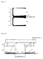
Fig. 10 , light traveling in thelight guide 21 comes into collision with alight scatterer 23 and therefore changes its angle at which it travels in thelight guide 21. This breaks all reflection conditions. Then, the light is emitted from theemission surface 21d or acounter surface 21e opposite theemission surface 21d to the outside of thelight guide 21. Here, assume that a space between thecounter surface 21e and the reflectingsheet 11 is substantially small. In this case, as indicated by a solid line arrow inFig. 10 , light having been emitted from thecounter surface 21e of thelight guide 21 is reflected by the reflectingsheet 11, and then re-enters thelight guide 21. The light having re-entered thelight guide 21 is reflected by aside wall surface 21g and is then re-emitted from theemission surface 21d. - As a result of this, it is difficult that the light reaches an area of the diffusing
plate 15 above thegap 22 between the light guides 21. That is, as shown inFig. 9 , the area of the diffusingplate 15 right above thegap 22 becomes dark. Therefore, the luminance unevenness occurs. - In the present embodiment, in order to prevent the occurrence of luminance unevenness in the
gap 22, as shown inFig. 5 , thin-walled parts walled parts 21c, which serve as center parts of cross sections that are orthogonal to the longer sides of the light guides 21. As such, thelight guide 21 of the present embodiment is substantially T-shaped in cross section because it has anabsent part 21f in the side end part on the emission side or on the reflecting sheet side, and thelight guide 21 consists of the thick-walled part 21c, which is formed to be thicker, and the thin-walled part 21b, which is formed to be thinner. In the present embodiment, the light guides 21 are disposed in such a manner that the thin-walled part 21b is nearer to the reflectingsheet 11. That is, theabsent parts 21f are provided on light emission sides of the light guides 21. - The following will describe why the above arrangement can prevent the occurrence of luminance unevenness.
- As shown in
Fig. 5 , assume that theabsent parts 21f are provided on light emission sides of the light guides 21. In this case, as indicated by a broken line arrow inFig. 5 , light traveling in the thick-walled part 21c of thelight guide 21 comes into collision with thelight scatterer 23 and therefore changes its angle at which it travels in thelight guide 21. This breaks all the reflection conditions. Then, the light is emitted from theemission surface 21d to the outside of thelight guide 21 and travels toward the diffusingplate 15. However, through such an optical path, the light does not reach an area of the diffusingplate 15 above the center of thegap 22. - Meanwhile, in the case where there exist the
absent parts 21f on the emission sides in the thin-walled parts 21b of the respective light guides 21, a large space between theemission surface 21d and the diffusingplate 15 can be provided by theabsent parts 21f in the vicinity of thegap 22. As such, as indicated by a solid line arrow inFig. 5 , light traveling in thelight guide 21 comes into collision with thelight scatterer 23 and therefore changes its angle at which it travels in thelight guide 21. This breaks all the reflection conditions. Then, the light is reflected by the reflectingsheet 11, which is provided below thecounter surface 21e, and is emitted from theemission surface 21d of the thin-walled part 21b to the outside of thelight guide 21. This makes it possible to easily illuminate the area of the diffusingplate 15 above thegap 22. Therefore, the unevenness in thegap 22 is less likely to occur. - Further, in the present embodiment, the diffusing
plate 15 is provided above theemission surface 21d of the light guides 21 so that a space D of 2mm, for example, is left between the diffusingplate 15 and theemission surface 21d of thelight guide 21. With this arrangement, it is possible to reduce the luminance unevenness, as compared with the arrangement in which the diffusingplate 15 is brought into intimate contact with theemission surface 21d of thelight guide 21. - Thus, the
light source module 10 of the present embodiment includes: the plurality of light guides 21 being provided such that longer sides thereof are arranged in parallel with each other with agap 22 therebetween; the plurality ofLEDs 12 each of which causes light to be directed from at least oneend surface 2 1 a of the light guides 21 in the longitudinal direction of the light guides 21; and the plurality oflight scatterers 23, as optical path changing sections, being provided on the light emission side of the light guides 21 or on the reflectingsheet 11 side opposite the light emission side, to extract light guided inside thelight guide 21. Besides, the thin-walled parts 21b, which serve as side end parts of cross sections orthogonal to the longer sides of the light guides 21, are formed to be thinner than the thick-walled parts 21c, which serve as center parts of the cross sections orthogonal to the longer sides of the light guides 21. - That is, in the side-edge type (also referred to as side-light type)
light source module 10, the plurality of light guides 21 constituting thelight guide plate 20 are provided such that longer sides thereof are arranged in parallel with each other with agap 22 therebetween. This causes low irradiance in thegap 22, resulting in the occurrence of luminance unevenness in the entire light guide plate. - However, the thin-
walled parts 21b in cross sections orthogonal to the longer sides of the light guides 21, are formed to be thinner than the thick-walled parts 21c in the cross sections orthogonal to the longer sides of the light guides 21. This forms theabsent parts 21f in the thin-walled parts 21b of the light guides 21. - With this arrangement, in the thin-
walled parts 21b of the respective light guides 21, (i) light having been emitted from thelight guide 21 or (ii) reflected light resulting from reflection of the light (i) by the reflectingsheet 11 passes through theabsent part 21f of thelight guide 21, thereby enabling illumination of thegap 22 between light guides 21 without re-entering thelight guide 21. - Therefore, it is possible to provide the
light source module 10 that enables avoiding lack of luminance in thegap 22 and enables reduction in the occurrence of luminance unevenness. - Further, in the
light source module 10 of the present embodiment, provision of theabsent parts 21f on the emission sides of the respective light guides 21 enables the thin-walled parts 21b of the respective light guides 21 to be formed thin. - With this, in the thin-
walled parts 21b of the respective light guides 21, the light having been emitted from thelight guide 21 passes through theabsent part 21f of thelight guide 21, thereby enabling illumination of the gap between the light guides 21 without re-entering thelight guide 21. - According to the arrangement shown in
Fig. 5 , even when thegap 22 between the light guides 21 increases to some degree, it is possible to curb the lower luminance. However, if the light guides 21 are directly disposed without being fixed, the light guides 21 are displaced from predetermined positions. This causes luminance unevenness, resulting in difficulty in properly performing a pseudo impulse-type display. - In view of this, in the present embodiment, as shown in
Fig. 2 , a plurality ofsupports 31 for supporting the light guides 21 at predetermined positions are provided below the light guide plate 20 (on the reflectingsheet 11 side). - As shown in
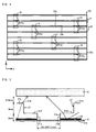
Fig. 1 , thesupport 31 has fixingmembers 31a that make onelight guide 21 caught therebetween to fix thelight guide 21. The following description assumes that twolight guides 21 are supported by onesupport 31 in the present embodiment. A shape of thesupport 31 will be described in detail later. - In a case where the
support 31, which is provided to support thelight guide 21, is made from a material that blocks light emitted from thelight guide 21, light having been emitted from thelight guide 21 does not illuminate the diffusingplate 15 in an area where thesupport 31 is provided. This results in lower luminance. - In order to curb the occurrence of luminance unevenness caused by provision of the
support 31 as described above, thesupport 31 is formed from a light-transmissive and light-scattering material. This material is preferably a material having a light-scattering property, as in the case with the diffusingplate 15 disposed above the light emission surface. - As such, the
support 31 is formed from a light-transmissive and light-scattering material. This makes it possible to curb the occurrence of luminance unevenness caused by thesupport 31, particularly, the occurrence of luminance unevenness caused by the fixingmembers 31a of thesupport 31. The reason for this will be described below. - As shown in
Fig. 1 , thesupport 31 is provided in such a manner that the fixingmember 31a is disposed in a space (gap 22) between the thin-walled parts 21b of the respective light guides 21. In a case where thesupport 31 provided in thegap 22 between the light guides 21 is made from a material that does not allow light to pass through it (highly reflective polycarbonate, etc.), as described in BACKGROUND ART, light emitted from theside wall surface 21g of thelight guide 21 is blocked by thesupport 31. This clearly forms light and dark patterns in and around thesupport 31, resulting in luminance unevenness. This means the occurrence of luminance unevenness caused by the fixingmember 31a of thesupport 31. - On the other hand, the
support 31, by virtue of its light-transmissive property, does not block the light emitted from theside wall surface 2 1 g of thelight guide 21. In addition, by virtue of its light-scattering property, thesupport 31 scatters the light emitted from theside wall surface 21g. This makes it possible to irradiate thegap 22 between the light guides 21 with light having uniform luminance. - Consequently, it is possible to reduce the occurrence of luminance unevenness caused by the
support 31 that is provided to support the light guides 21 at predetermined intervals, particularly the occurrence of luminance unevenness caused by the fixingmembers 31 a. - Further, the fixing
members 31a of thesupport 31 are each disposed between the light guides 21, and make onelight guide 21 caught therebetween so as to fix thelight guide 21. - With this arrangement, the fixing
member 31a exists in thegap 22 between the light guides 21. This ensures the light guides 21 to be supported at predetermined intervals. - Still further, since the
support 31 is made from a material having the same optical properties as the diffusingplate 15, the optical properties of thesupport 31 become equal to those of the diffusingplate 15. This makes it possible to make lower luminance in the gap between the light guides 21 less noticeable. - As a result of this, it is possible to attempt further decrease in luminance unevenness in the light emission surface of the light source module.
- For example, with use of (i) the
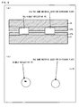
support 31 produced from a highly reflective PC (polycarbonate) and (ii) thesupport 31 produced from the same material used for the diffusingplate 15, the degrees of luminance unevenness that occur around both of thesupports 31 have been evaluated. The evaluation results are shown in (a) and (b) ofFig. 6 . - (a) of
Fig. 6 is a plan view of light guides 21 when seen from above in a state where the diffusing plate is removed, and shows the state where the fixingmembers 31a produced from different materials are exposed. (b) ofFig. 6 is a view when the plan view showing the state shown in (a) ofFig. 6 is seen through the diffusingplate 15. - As is clear from (b) of
Fig. 6 , the fixingmember 31a produced from the same material used for the diffusingplate 15 does not block light from the light guides, and therefore enables curbing luminance unevenness caused by lower luminance. - As described previously, the
support 31 is preferably produced from the same material used for the diffusingplate 15 that is used together with thesupport 31, from the viewpoint of reducing luminance unevenness. However, to yield the effect of reducing luminance unevenness caused by thesupport 31, thesupport 31 produced from a light-transmissive and light-scattering material is good enough. - The material for the
support 31 is preferably the same as that for the diffusingplate 15, which is a diffusing member. Therefore, the material for thesupport 31 is PC (polycarbonate), PS (polystyrene), PMMA (polymethylmethacrylate), or the like, all of which can be a possible material for the diffusingplate 15. Alternatively, thesupport 31 may be formed from a material using scattering property of the material itself, a light-transmissive material containing scattering components such as silica, or a material having a surface that exerts scattering property. However, the materials for the diffusingplate 15 and thesupport 31 as used in the present invention are not limited to the above-described materials, provided that they are light-scattering and light-transmissive materials. For example, a knit of light-transmissive fibers, etc. may be used as light-scattering materials. - The problems associated with the above arranged
light source module 10 are not only the occurrence of luminance unevenness caused by the material for thesupport 31, but also the occurrence of luminance unevenness caused by displacement of the light guides from predetermined positions. For example, even though the material for thesupport 31 is appropriately selected for an attempt to curb lower luminance, displacement of the light guides from the predetermined positions causes luminance unevenness in the emission surface of the light source module. Thus, the occurrence of luminance unevenness in the emission surface of the light source module interferes with proper pseudo impulse-type display in a liquid crystal display apparatus. This results in degradation in display quality. - The following will describe the shapes of the
support 31, for fixing the light guides 21 at predetermined positions with reliability. - For example, as shown in
Figs. 7(a) through 7(d) , thesupport 31 is arranged as follows. That is, the fixingmembers 31a are provided at both ends and center of a light guide support surface (front surface) of a substantiallyrectangular base 31c. In addition, latches 31b are provided at both sides and center of the back surface of the base (fixing plate) 31c. - The fixing
members 31a provided at one of the ends of the front surface of thebase 31c and at the center of the front surface of thebase 31c make onelight guide 21 caught therebetween so as to support and fix thelight guide 21, while the fixingmembers 31a provided at the other end of the front surface of thebase 31c and at the center of the front surface of thebase 31c make anotherlight guide 21 caught therebetween so as to support and fix thelight guide 21. Therefore, in the above example, twolight guides 21 are supported and fixed by onesupport 31. - Further, the
latches 31b provided on the back surface of thebase 31c are engaged in corresponding latch holes (not shown) provided on the chassis 2 (Fig. 2 ), so that thesupport 31 is fixed to thechassis 2. - To fix the
support 31 to thechassis 2, part of the reflectingsheet 11 provided between thesupport 31 and thechassis 2 needs to have openings. For example, openings are provided in the reflectingsheet 11 so that only the fixingmembers 31a of thesupport 31 can be protruded, and thebase 31c is positioned under the reflecting sheet. As compared with the arrangement in which thesupport 31 is merely disposed on the reflectingsheet 11, the above arrangement eliminates the difference in surface level (irregularities) between the reflectingsheet 11 and the base 31c of thesupport 31, and enables the surface of the reflectingsheet 11 where thesupport 31 is formed to be kept flat, which thus eliminates reflection unevenness on the reflectingsheet 11. - The fixing
member 31a is formed in such a shape that an edge part thereof is bent toward the side on which thelight guide 21 is caught. As shown inFig. 7(b) , the edge part pushes down the thin-walled part 21b of thelight guide 21. - However, the arrangement of the fixing
member 31a as shown inFig. 7(b) such that the thin-walled part 2 1 b of thelight guide 21 is pushed down from above may give rise to the following problems. That is, it is difficult to adjust the amount of force with which the thin-walled part 21b is pushed down. Further, if the force is weaker, thelight guide 21 is not sufficiently fixed by thebase 31c, and if the force is stronger, the thin-walled part 2 1 b is damaged. - In view of this, as shown in
Figs. 8(a) through 8(c) , for example, the fixingmember 31a can be made bow-shaped in cross section, so that the thin-walled part 21b of thelight guide 21 is caught by a bow-shaped protrusion. Note that the components of thesupport 31 shown inFigs. 8(a) through 8(c) have the same shapes as those of thesupport 31 shown inFigs. 7(a) through 7(c) , except for the shape of the fixingmember 31a. - According to the
support 31 arranged as shown inFigs. 8(a) through 8(c) , the fixingmembers 31a are formed from an elastic material that energizes in such a direction that thelight guide 21 is caught therebetween. This means that the fixingmembers 31a energize the side surface of the thin-walled part 21b of thelight guide 21, not the upper surface of the thin-walled part 21b, which enables thelight guide 21 to be reliably fixed without a risk of damage to the thin-walled part 21b. - Therefore, with use of the above-arranged
support 31, it is possible to reliably prevent the light guides 21 from being displaced in the above-arrangedlight source module 10. Thus, it is possible to curb the occurrence of luminance unevenness caused by the displacement. This, in turn, curbs the occurrence of luminance unevenness in the emission surface of thelight source module 10, which enables a liquid crystal display apparatus to perform pseudo impulse-type display in a proper manner. - The present invention is not limited to the aforementioned embodiments and is susceptible of various changes within the scope of the accompanying claims. Also, an embodiment obtained by suitable combinations of technical means disclosed in the different embodiments are also included within the technical scope of the present invention.
- The present invention relates to: a light source module provided with a side-edge type (also referred to as side-light type) light guide plate through which light from a light source is planarly emitted; and an electronic apparatus including the light source module. For example, the present invention is applicable to a planar light source device as a light source module such as a backlight, and an electronic apparatus such as a liquid crystal display apparatus.
-
- 1
- Liquid crystal display apparatus (electronic apparatus)
- 2
- Chassis
- 3
- Liquid crystal panel
- 4
- Bezel
- 10
- Light source module (planar light source device)
- 11
- Reflecting sheet
- 12
- LED (light source)
- 13
- LED substrate
- 14
- Reflector
- 15
- Diffusing plate (optical path changing section)
- 16
- Optical sheet group
- 20
- Light guide plate
- 21
- Light guide
- 2 1a
- End surface
- 2 1 b
- Thin-walled part
- 2 1 c
- Thick-walled part
- 21d
- Emission surface
- 21e
- Counter surface
- 21f
- Absent part
- 21g
- Side wall surface
- 22
- Gap
- 23
- Light scatterer (optical path changing section)
- 31
- Support
- 31a
- Fixing member
- 31b
- Latch
- 31c
- Base (fixing plate)
Claims (4)
- A planar light source device, comprising:a plurality of light guides being provided such that longer sides thereof are arranged in parallel with each other with a gap therebetween;a plurality of light sources each of which causes light to be directed from at least one of opposite end surfaces of the light guide in the longitudinal direction of the light guide;a plurality of optical path changing sections being provided on a light emission side of the light guide or on a reflecting sheet side opposite the light emission side, to extract light guided inside the light guide; andsupports for supporting the light guides at predetermined intervals,the supports being made from a light-transmissive and light-scattering material.
- A planar light source device, comprising:a plurality of light guides being provided such that longer sides thereof are arranged in parallel with each other with a gap therebetween;a plurality of light sources each of which causes light to enter at least one of opposite end surfaces of the light guide in the longitudinal direction of the light guide;a plurality of optical path changing sections being provided on a light emission side of the light guide or on a reflecting sheet side opposite the light emission side, to extract light guided inside the light guide;a diffusing member which diffuses light emitted from the light guides; andsupports for supporting the light guides at predetermined intervals,the supports having the same optical properties as the diffusing member.
- The planar light source device according to claim 1 or 2, whereineach of the supports has fixing members disposed between the light guides, andthe fixing members make one light guide caught therebetween to fix the light guide.
- The planar light source device according to claim 3, whereinthe fixing members are made from an elastic material that energizes the light guide to be caught between the fixing members.
Applications Claiming Priority (2)
| Application Number | Priority Date | Filing Date | Title |
|---|---|---|---|
| JP2009235739A JP4560579B1 (en) | 2009-10-09 | 2009-10-09 | Surface light source device |
| PCT/JP2010/000552 WO2011043003A1 (en) | 2009-10-09 | 2010-01-29 | Surface light source device |
Publications (1)
| Publication Number | Publication Date |
|---|---|
| EP2351962A1 true EP2351962A1 (en) | 2011-08-03 |
Family
ID=43048763
Family Applications (1)
| Application Number | Title | Priority Date | Filing Date |
|---|---|---|---|
| EP10734887A Withdrawn EP2351962A1 (en) | 2009-10-09 | 2010-01-29 | Surface light source device |
Country Status (8)
| Country | Link |
|---|---|
| US (1) | US8303153B2 (en) |
| EP (1) | EP2351962A1 (en) |
| JP (1) | JP4560579B1 (en) |
| CN (1) | CN102105739A (en) |
| BR (1) | BRPI1001230A2 (en) |
| MX (1) | MX2010008348A (en) |
| RU (1) | RU2010132150A (en) |
| WO (1) | WO2011043003A1 (en) |
Families Citing this family (16)
| Publication number | Priority date | Publication date | Assignee | Title |
|---|---|---|---|---|
| JP4781483B1 (en) * | 2010-02-26 | 2011-09-28 | シャープ株式会社 | Light guide plate device, light source device, display device, and television receiver |
| KR101769045B1 (en) * | 2010-06-14 | 2017-08-17 | 엘지이노텍 주식회사 | Display device |
| US8801261B2 (en) * | 2010-06-24 | 2014-08-12 | Sharp Kabushiki Kaisha | Backlight unit and liquid crystal display device |
| JP5699808B2 (en) * | 2011-05-27 | 2015-04-15 | 株式会社リコー | Light guide member, document illumination device, image reading device, and image forming device |
| CN102654260B (en) | 2011-09-29 | 2014-09-03 | 北京京东方光电科技有限公司 | Backlight source and liquid crystal display (LCD) |
| CN102865511A (en) * | 2012-09-14 | 2013-01-09 | 深圳市华星光电技术有限公司 | Direct type backlight module |
| JP2014082065A (en) * | 2012-10-15 | 2014-05-08 | Skg:Kk | Light guide member |
| KR101454757B1 (en) * | 2012-10-29 | 2014-10-27 | 코닝정밀소재 주식회사 | Light diffusing plate, method for manufacturing the same, and led illumination apparatus comprising the same |
| KR101405049B1 (en) * | 2013-02-08 | 2014-06-13 | 희성전자 주식회사 | Backloght Unit |
| CN103672746B (en) * | 2013-12-20 | 2017-01-11 | 深圳市华星光电技术有限公司 | Light guide plate, backlight module and liquid crystal display device |
| DE202014000264U1 (en) * | 2014-01-10 | 2015-04-13 | Novomatic Ag | lighting device |
| US9563005B2 (en) * | 2014-03-11 | 2017-02-07 | Sakai Display Products Corporation | Light source device, display apparatus, and method of manufacturing light source device |
| JP6205647B2 (en) * | 2014-05-23 | 2017-10-04 | コニカミノルタ株式会社 | Light guide, illumination device, and image reading device |
| CN204853358U (en) * | 2015-08-11 | 2015-12-09 | 合肥京东方显示光源有限公司 | Limit structure , backlight unit and display device |
| JP7368750B2 (en) | 2021-07-29 | 2023-10-25 | 日亜化学工業株式会社 | Light emitting module and planar light source |
| JP2023096907A (en) * | 2021-12-27 | 2023-07-07 | シャープディスプレイテクノロジー株式会社 | liquid crystal display element |
Family Cites Families (9)
| Publication number | Priority date | Publication date | Assignee | Title |
|---|---|---|---|---|
| CN100485487C (en) | 2002-04-22 | 2009-05-06 | 三菱丽阳株式会社 | Surface light source device and light guide for surface light source device |
| JP4716754B2 (en) | 2005-02-25 | 2011-07-06 | 三菱レイヨン株式会社 | Surface light source device, light guide used therefor, and manufacturing method thereof |
| WO2007138763A1 (en) | 2006-06-01 | 2007-12-06 | Sharp Kabushiki Kaisha | Surface-area light source device and liquid crystal display device using the same |
| JP4695626B2 (en) | 2006-06-30 | 2011-06-08 | 株式会社東芝 | Illumination device and liquid crystal display device |
| US7780330B2 (en) * | 2007-05-16 | 2010-08-24 | Rohm And Haas Electronics Materials Llc | Elongated illuminators configuration for LCD displays |
| CN101329472B (en) | 2007-06-18 | 2010-11-03 | 奇菱科技股份有限公司 | Light emitting device and method for manufacturing the same |
| JP2009110794A (en) * | 2007-10-30 | 2009-05-21 | Goyo Paper Working Co Ltd | Surface light source and light guide used for surface light source |
| US8047669B2 (en) * | 2009-07-31 | 2011-11-01 | Skc Haas Display Films Co., Ltd. | Backlight illumination assembly having a joining clip with diffusion means |
| JP2011040278A (en) * | 2009-08-11 | 2011-02-24 | Sony Corp | Planar illumination device |
-
2009
- 2009-10-09 JP JP2009235739A patent/JP4560579B1/en not_active Expired - Fee Related
-
2010
- 2010-01-29 MX MX2010008348A patent/MX2010008348A/en active IP Right Grant
- 2010-01-29 BR BRPI1001230A patent/BRPI1001230A2/en not_active IP Right Cessation
- 2010-01-29 WO PCT/JP2010/000552 patent/WO2011043003A1/en not_active Ceased
- 2010-01-29 CN CN2010800010431A patent/CN102105739A/en active Pending
- 2010-01-29 EP EP10734887A patent/EP2351962A1/en not_active Withdrawn
- 2010-01-29 US US12/865,313 patent/US8303153B2/en not_active Expired - Fee Related
- 2010-01-29 RU RU2010132150/07A patent/RU2010132150A/en not_active Application Discontinuation
Non-Patent Citations (1)
| Title |
|---|
| See references of WO2011043003A1 * |
Also Published As
| Publication number | Publication date |
|---|---|
| WO2011043003A1 (en) | 2011-04-14 |
| BRPI1001230A2 (en) | 2016-09-27 |
| JP4560579B1 (en) | 2010-10-13 |
| US8303153B2 (en) | 2012-11-06 |
| US20120182761A1 (en) | 2012-07-19 |
| CN102105739A (en) | 2011-06-22 |
| RU2010132150A (en) | 2013-11-20 |
| MX2010008348A (en) | 2011-05-27 |
| JP2011082123A (en) | 2011-04-21 |
Similar Documents
| Publication | Publication Date | Title |
|---|---|---|
| US8303153B2 (en) | Planar light source device | |
| US8674929B2 (en) | Optical assembly, backlight unit including the same, and display apparatus including the backlight unit | |
| US20120212690A1 (en) | Backlight device and liquid crystal display | |
| EP2557351A1 (en) | Light source module and electronic apparatus provided with same | |
| KR20060105346A (en) | Backlight unit and LCD using the same | |
| US20120275192A1 (en) | Light source module and electronic apparatus including the same | |
| KR101584280B1 (en) | Light guide plate and display apparatus having the same | |
| JP4607225B2 (en) | Light source module, liquid crystal display device and lighting device | |
| KR102898259B1 (en) | Backlight unit capable of local dimming | |
| WO2013181865A1 (en) | Edge-lighting backlight module | |
| CN101317038A (en) | Backlight device and liquid crystal display device using the backlight device | |
| JP2012119252A (en) | Liquid crystal display apparatus | |
| JP2010192301A (en) | Backlight device, and liquid crystal display using the same | |
| JP4695710B1 (en) | Surface light source device and electronic device including the same | |
| KR20080095576A (en) | Direct type backlight unit | |
| KR101331904B1 (en) | Light emitting diode array and and backlight unit using the same | |
| EP2487403A1 (en) | Light source module and electronic apparatus provided with same | |
| KR20100122656A (en) | Light guide plate and backlight unit having the same | |
| EP2484953A1 (en) | Light source module and electronic apparatus with same | |
| JP4585989B2 (en) | Backlight, liquid crystal display element | |
| EP2487402A1 (en) | Light source module and electronic apparatus provided with same | |
| KR20110037727A (en) | Liquid crystal display | |
| KR101837775B1 (en) | Liquid Crystal Display | |
| KR101296456B1 (en) | Back light Unit and Liquid Crystal Display using the same | |
| US20110221977A1 (en) | Light source unit, lighting device, display device and television receiver |
Legal Events
| Date | Code | Title | Description |
|---|---|---|---|
| PUAI | Public reference made under article 153(3) epc to a published international application that has entered the european phase |
Free format text: ORIGINAL CODE: 0009012 |
|
| 17P | Request for examination filed |
Effective date: 20100729 |
|
| AK | Designated contracting states |
Kind code of ref document: A1 Designated state(s): AT BE BG CH CY CZ DE DK EE ES FI FR GB GR HR HU IE IS IT LI LT LU LV MC MK MT NL NO PL PT RO SE SI SK SM TR |
|
| DAX | Request for extension of the european patent (deleted) | ||
| STAA | Information on the status of an ep patent application or granted ep patent |
Free format text: STATUS: THE APPLICATION HAS BEEN WITHDRAWN |
|
| 18W | Application withdrawn |
Effective date: 20130516 |