EP2346166A1 - Elastic wave filter device and module comprising the elastic wave filter device - Google Patents
Elastic wave filter device and module comprising the elastic wave filter device Download PDFInfo
- Publication number
- EP2346166A1 EP2346166A1 EP09824669A EP09824669A EP2346166A1 EP 2346166 A1 EP2346166 A1 EP 2346166A1 EP 09824669 A EP09824669 A EP 09824669A EP 09824669 A EP09824669 A EP 09824669A EP 2346166 A1 EP2346166 A1 EP 2346166A1
- Authority
- EP
- European Patent Office
- Prior art keywords
- ground
- elastic wave
- wave filter
- output
- input
- Prior art date
- Legal status (The legal status is an assumption and is not a legal conclusion. Google has not performed a legal analysis and makes no representation as to the accuracy of the status listed.)
- Granted
Links
Images




Classifications
-
- H—ELECTRICITY
- H03—ELECTRONIC CIRCUITRY
- H03H—IMPEDANCE NETWORKS, e.g. RESONANT CIRCUITS; RESONATORS
- H03H9/00—Networks comprising electromechanical or electro-acoustic elements; Electromechanical resonators
- H03H9/46—Filters
- H03H9/64—Filters using surface acoustic waves
- H03H9/6423—Means for obtaining a particular transfer characteristic
- H03H9/6433—Coupled resonator filters
- H03H9/6436—Coupled resonator filters having one acoustic track only
-
- H—ELECTRICITY
- H03—ELECTRONIC CIRCUITRY
- H03H—IMPEDANCE NETWORKS, e.g. RESONANT CIRCUITS; RESONATORS
- H03H9/00—Networks comprising electromechanical or electro-acoustic elements; Electromechanical resonators
- H03H9/46—Filters
- H03H9/64—Filters using surface acoustic waves
-
- H—ELECTRICITY
- H03—ELECTRONIC CIRCUITRY
- H03H—IMPEDANCE NETWORKS, e.g. RESONANT CIRCUITS; RESONATORS
- H03H9/00—Networks comprising electromechanical or electro-acoustic elements; Electromechanical resonators
- H03H9/02—Details
- H03H9/05—Holders or supports
- H03H9/058—Holders or supports for surface acoustic wave devices
-
- H—ELECTRICITY
- H03—ELECTRONIC CIRCUITRY
- H03H—IMPEDANCE NETWORKS, e.g. RESONANT CIRCUITS; RESONATORS
- H03H9/00—Networks comprising electromechanical or electro-acoustic elements; Electromechanical resonators
- H03H9/02—Details
- H03H9/125—Driving means, e.g. electrodes, coils
- H03H9/145—Driving means, e.g. electrodes, coils for networks using surface acoustic waves
-
- H—ELECTRICITY
- H03—ELECTRONIC CIRCUITRY
- H03H—IMPEDANCE NETWORKS, e.g. RESONANT CIRCUITS; RESONATORS
- H03H9/00—Networks comprising electromechanical or electro-acoustic elements; Electromechanical resonators
- H03H9/46—Filters
- H03H9/64—Filters using surface acoustic waves
- H03H9/6423—Means for obtaining a particular transfer characteristic
- H03H9/6433—Coupled resonator filters
- H03H9/644—Coupled resonator filters having two acoustic tracks
-
- H—ELECTRICITY
- H03—ELECTRONIC CIRCUITRY
- H03H—IMPEDANCE NETWORKS, e.g. RESONANT CIRCUITS; RESONATORS
- H03H9/00—Networks comprising electromechanical or electro-acoustic elements; Electromechanical resonators
- H03H9/46—Filters
- H03H9/64—Filters using surface acoustic waves
- H03H9/6489—Compensation of undesirable effects
- H03H9/6493—Side lobe suppression
-
- H—ELECTRICITY
- H03—ELECTRONIC CIRCUITRY
- H03H—IMPEDANCE NETWORKS, e.g. RESONANT CIRCUITS; RESONATORS
- H03H9/00—Networks comprising electromechanical or electro-acoustic elements; Electromechanical resonators
- H03H9/70—Multiple-port networks for connecting several sources or loads, working on different frequencies or frequency bands, to a common load or source
- H03H9/72—Networks using surface acoustic waves
-
- H—ELECTRICITY
- H03—ELECTRONIC CIRCUITRY
- H03H—IMPEDANCE NETWORKS, e.g. RESONANT CIRCUITS; RESONATORS
- H03H9/00—Networks comprising electromechanical or electro-acoustic elements; Electromechanical resonators
- H03H9/70—Multiple-port networks for connecting several sources or loads, working on different frequencies or frequency bands, to a common load or source
- H03H9/72—Networks using surface acoustic waves
- H03H9/725—Duplexers
Definitions
- the invention relates to an elastic wave filter device including an elastic wave filter and a parallel trap that are connected to each other in a pattern on a piezoelectric substrate, and also relates to a module including the elastic wave filter device.
- Elastic wave filter devices that use electromechanical vibration, such as surface elastic waves using vibration on a surface of a piezoelectric substrate, bulk acoustic waves using vibration inside a piezoelectric substrate, and boundary acoustic waves using vibration on an interface of a laminated piezoelectric substrate, are used for RF filters or the like of mobile phone apparatuses.
- An example of the elastic wave filter device includes a device in which a plurality of one-port elastic wave resonators (hereinafter simply referred to as resonators) are arranged in an elastic wave propagation direction and are longitudinally coupled to form a multimode filter, and trap resonators are inserted into the multimode filter in series and in parallel to form a ladder-pattern connection (e.g., see Patent Document 1).
- resonators one-port elastic wave resonators
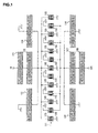
- Fig. 1 is a circuit illustrating an example configuration of a conventional elastic wave filter device.
- This elastic wave filter device includes a multimode filter 111, which is made up of a plurality of resonators 105 and a plurality of resonators 106, and also includes series trap resonators 101, 102, 017, and 108 and parallel trap resonators 103, 104, 109, and 110.
- first IDT electrodes are connected so input lines, and individual second IDT electrodes are connected to ground lines.
- individual first IDT electrodes are connected to output lines, and individual second IDT electrodes are connected to ground lines.
- the plurality of resonators 105 and 106 are alternately arranged in an elastic wave propagation direction and are longitudinally coupled, thereby forming the multimode filter 111.
- the series trap resonators 101 and 102 are inserted in series into an input line, and the series trap resonators 107 and 108 are inserted in series into an output line.
- the parallel trap resonators 103 and 104 are inserted in parallel between input lines and ground lines, and the parallel trap resonators 109 and 110 are inserted in parallel between output lines and ground lines.
- Such an elastic wave filter device is normally formed as a chip that is integrally provided on a piezoelectric substrate.
- the chip of this elastic wave filter device is mounted on a module body, such as a ceramic substrate or a printed board, so as to be formed as a module.
- a module body such as a ceramic substrate or a printed board
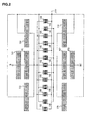
- all the ground lines are commonly connected to a single ground connection electrode.
- the wiring on a module body extending from external terminals of the module to the elastic wave filter device has a parasitic impedance.
- a ground connection electrode provided on a or a piezoelectric substrate is connected to an external ground terminal of the module via the parasitic impedance.
- the effect of the parasitic impedance may the attenuation characteristic and isolation characteristic of an elastic wave filter.
- an object of the present invention is to provide an elastic wave filter device capable of suppressing degradation of the attenuation characteristic and isolation characteristic of a filter, the degradation affecting the elastic wave filter device due to the effect of the parasitic impedance of connection wiring, and to provide a module including the elastic wave filter device.
- the present invention is an elastic wave filter device in which an elastic wave filter and a parallel trap are provided on a piezoelectric substrate, and includes a first ground connection electrode and a second ground connection electrode.
- the elastic wave filter includes input-side resonators and output-side resonators coupled to each other. Each of the input-side resonators is connected between an input line and a ground line. Each of the output-side resonators is connected between an output line and a ground line.
- the parallel trap is connected between a ground line and the input line or the output line.
- the first ground connection electrode is provided on a surface of the piezoelectric substrate and is connected to the ground lines of the input-side resonators and the ground lines of the output-side resonators.
- the second ground connection electrode is provided on the surface of the piezoelectric substrate so as to be isolated from the first ground connection electrode and is connected to the ground line of the parallel trap.
- the plurality of resonators of the elastic wave filter are connected to the first ground connection electrode on the surface of the piezoelectric substrate, and the parallel trap is connected to the second ground connection electrode isolated from the ground connection electrode.
- the parasitic impedance of connection wiring with respect to the first ground connection electrode commonly affects the plurality of resonators of the elastic wave filter.
- the parasitic impedance of connection wiring with respect to the second ground connection electrode is independent of the parasitic impedance that affects the elastic wave filter and affects only the parallel trap.
- each of the input-side resonators and the output-side resonators includes a first IDT electrode connected to an input/output line and a second IDT electrode connected to a ground line.
- the input-side resonators and the output-side resonators are alternately arranged in an elastic wave propagation direction
- the first IDT electrodes and the second IDT electrodes are arranged in a direction orthogonal to the elastic wave propagation direction
- the arrangement order of the first IDT electrodes and the second IDT electrodes in the input-side resonators is opposite to the arrangement order in the output-side resonators.
- the first IDT electrodes of the input-side resonators and the second IDT electrodes of the output-side resonators are arranged on both sides of the elastic wave filter.
- the circuit configuration is likely to be simplified by connecting the second IDT electrodes of the input-side resonators and the second IDT electrodes of the output-side resonators to different ground connection electrodes. In that case, however, degradation of the attenuation characteristic and isolation characteristic of the filter occurs due to the effect of parasitic impedance if the filter is integrated into a module. Therefore, even in the case of this configuration, it is preferable that the individual second IDT electrodes be connected to a common ground connection electrode.
- a module according to the present invention includes the above-described elastic wave filter device and a module body on which the elastic wave filter device is mounted.
- the module body may include, on a mounting surface thereof, a ground terminal connected to the first ground connection electrode and the second ground connection electrode.
- the parasitic impedance caused by connection wiring with respect to the first ground connection electrode of the elastic wave filter device commonly the plurality of resonators of the elastic wave filter, and is independent of the parasitic impedance that affects the parallel trap. Accordingly, degradation of the attenuation characteristic and isolation characteristic of the filter can be suppressed.
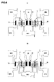
- Fig. 3 includes diagrams illustrating a schematic configuration of a module including an elastic wave filter according to a first embodiment.
- Fig. 3(A) is a cross-sectional view of a main part of the module, and
- Fig. 3(B) is a circuit diagrams the module.
- the module 100 has a configuration in which a chip of an elastic wave filter device 1 is mounted on a module body 20, which is made up of a laminated substrate having a five-layer structure.
- the module body 20 includes mounting terminals (described below) provided on a mounting surface opposite to a chip mounting surface, and internal wiring is formed therein for connecting the individual mounting terminals and the individual connection ports (connection electrodes) of the elastic wave filter device 1.
- the elastic wave falter device 1 is a chip of a SAW (surface acoustic wave) filter in which a transmission circuit TX and a reception circuit RX of a duplexer are provided on a circuit formation surface of a piezoelectric substrate 10. This chip is mounted on the module body 20 such that the circuit formation surface faces the module body 20, and the individual connection ports are connected to the electrodes of the module body 20 using bumps.
- SAW surface acoustic wave
- the transmission circuit TX is of an unbalanced input-unbalanced output type, and the connection port for transmission input of the transmission circuit TX is connected to a transmission input terminal Tx, which is a mounting terminal of the module body 20, via the internal wiring of the module body 20.
- the connection port for transmission output of the transmission circuit TX is connected to an antenna terminal Ant, which is a mounting terminal of the module body 20, via the internal wiring of the module body 20.
- the antenna terminal Ant is connected to a ground terminal Gnd2, which is a mounting terminal of the module body 20, via a coil provided as the internal wiring of the module body 20.
- the reception circuit RX is a reception circuit of an unbalanced input-balanced output type (balun type), and includes elastic wave filters 4 and 5, series resonators 2A and 2B, and parallel resonators 3A and 3B, which serve as a circuit element unit. Also, the reception circuit RX includes a reception input port IN, reception output ports OUT1 and OUT2, and ground ports GND1, GND2, and GND3, which serve as connection ports.
- the elastic wave filter 4 is a longitudinally coupled resonator SAW filter including five resonators 4A to 4E that are alternately arranged in an elastic wave propagation direction and are longitudinally coupled, and is connected between the reception input port IN and the reception output port OUT1.
- the elastic wave filter 5 is a longitudinally coupled resonator SAW filter including five resonators 5A to 5E that are alternately arranged in the elastic wave propagation direction and are longitudinally coupled, and is connected between the reception input port IN and the reception output port OUT2.
- the elastic wave filters 4 and 5 output signals with a phase difference, whereby the reception circuit RX obtains an unbalanced output.
- Each of the resonators 4A, 4C, 4E, 5A, 5C, and 5E is an input-side resonator, and includes a first IDT electrode (not illustrated) connected to an input line and a second IDT electrode (not illustrated) connected to a ground line.
- Each of the resonators 4B, 4D, 5B, and 5D is an output-side resonator, and includes a first IDT electrode (not illustrated) connected to an output line and a second IDT electrode (not illustrated) connected to a ground line.
- the ground lines connected to the respective resonators 4A to 4E and 5A to 5E are commonly connected to the ground port GND1, which is a first ground connection electrode according to the present invention.
- the output lines connected to the resonators 4B and 4D are commonly connected to the reception output port OUT1.
- the output lines connected to the resonators 5B and 5D are commonly connected to the reception output port OUT2.
- the series resonator 2A is inserted in series into an input line of the elastic wave filter 4, and the series resonator 2B is inserted in series into an input line of the elastic wave filter 5.
- Each of the series resonators 2A and 2B functions as a series trap. These input lines are commonly connected to the reception input port IN.
- the parallel resonator 3A is inserted into a parallel line that branches from an output line of the elastic wave filter 4 and functions as a parallel trap. This parallel line is connected to the ground port GND2, which is a second ground connection electrode according to the present invention.
- the parallel resonator 38 is inserted into a parallel line that branches from an output line of the elastic wave filter 5 and functions as a parallel trap. This parallel line is connected to the ground port GND3, which is the second ground connection electrode according to the present invention.
- the reception input port IN is connected to the antenna terminal Ant, which is a mounting terminal of the module body 20, via a reception input wiring line6 in the module body 20.
- the reception output ports OUT1 and OUT2 are connected to reception output terminals Rx1 and Rx2, which are mounting terminals of the module body 20, via reception output wirings line4 and line5 in the module body 20.
- the ground ports GND1, GND2, and GND3 are connected to a ground wiring line7 in the module body 20 via ground wirings line1, line2, and line3 in the module body 20, and are connected to a ground terminal Gnd1, which is a mounting terminal of the module body 20, via the ground wiring line7.
- all the ground lines connected to the elastic wave filters 4 and 5 are commonly connected to the ground port GND1 on the piezoelectric substrate 10. Also, the parallel line connected to the parallel resonator 3A is connected to the ground port GND2 and the parallel line connected to the parallel resonator 3B is connected to the ground port GND3 on the piezoelectric substrate 10.
- the parasitic impedance of the ground wiring line1 of the module body 20 commonly affects all the resonators of the elastic wave filters 4 and 5. Also, the parasitic impedance of the ground wirings line2 and line3 of the module body 20 is independent of the parasitic impedance that affects the elastic wave filters 4 and 5. Accordingly, degradation of the attenuation characteristic and isolation characteristic of the filters can be suppressed.
- Fig. 4 is a bottom view illustrating the circuit formation surface of the elastic wave filter device 1.
- Fig. 5 is an exploded view of electrode layers provided in the module body 20 viewed from the bottom.
- the elastic wave filter device 1 has a circuit pattern serving as the reception circuit RX and the transmission circuit TX provided on the circuit formation surface of the piezoelectric substrate 10. Also, the circuit pattern serving as the reception circuit RX is provided with a plurality of IDT electrodes serving as the elastic wave filters 4 and 5, the series resonators 2A and 2B, and the parallel resonators 3A and 3B.
- Each of the elastic wave filters 4 and 5 includes three input-side resonators and two output-side resonators, and the individual resonators are alternately arranged in the elastic wave propagation direction, which is the horizontal direction in the figure.
- each of the resonators includes a first IDT electrode connected to an input/output line and a second IDT electrode connected to a ground line.
- the first IDT electrodes and the second IDT electrodes are arranged in a direction orthogonal to the elastic wave propagation direction, which is the vertical direction in the figure.
- the first IDT electrode is arranged on the center side of the substrate and the second IDT electrode is arranged on the upper end side of the substrate (or on the lower end side of the substrate).
- the arrangement order is opposite.
- this circuit pattern includes an electrode portion serving as the reception input port IN, an electrode portion serving as the reception output port OUT1, an electrode portion serving as the reception output port OUT2, an electrode portion serving as the ground port GND1, an electrode portion serving as the ground port GND2, and an electrode portion serving as the ground port GND3.
- the electrodes corresponding to these respective connection ports are connected to the electrodes of the module body 20 via bump electrodes.
- the module body 20 includes six electrode layers (A) to (F) in order from the chip mounting surface to the mounting surface.
- the electrode layer (A) is provided on the chip mounting surface of the module body 20 and includes a plurality of electrodes on which the respective connection ports of the elastic wave filter devise 1 are mounted.
- the electrode layer (A) includes an electrode on which the reception input port IN of the reception circuit RX is mounted and which forms the reception input wiring line6, an electrode on which the reception output port OUT1 is mounted and which forms the reception output wiring line4, an electrode on which the reception output port OUT2 is mounted and which forms the reception output wiring line5, an electrode on which the ground port GND1 is mounted and which forms the ground wiring line1, an electrode on which the ground port GND2 is mounted and which forms the ground wiring line2, an electrode on which the ground port GND3 is mounted and which forms the ground wiring line3, and a plurality of electrodes to which the respective connection ports of the transmission circuit TX are connected.
- the electrode layer (B) is formed between the first-layer substrate and the second-layer substrate among the laminated substrates of the module body 20 and includes a plurality of electrodes connected to the respective electrodes of the electrode layer (A) via through holes.
- the electrode layer (B) includes an electrode which forms the reception input wiring line6 of the reception circuit RX, an electrode which forms the reception output wiring line4, an electrode which forms the reception output wiring line5, an electrode which forms the ground wiring line1, an electrode which forms the ground wiring line2, an electrode which forms the ground wiring line3, and a plurality of electrodes serving as the internal wiring of the transmission circuit TX.
- the electrode layer (C) is formed between the second-layer substrate and the third-layer substrate among the laminated substrates of the module body 20 and includes a plurality of connected to the respective electrodes of the electrode (B) via through holes.
- the electrode layer (C) includes an electrode which forms the reception input wiring line6 of the reception circuit RX, an electrode which forms the reception output wiring line4, an electrode which forms the reception output wiring line5, an internal ground connection electrode which connects the ground wiring line1, the ground wiring line2, and the ground wiring line3, and a plurality of electrodes serving as the internal wiring of the transmission circuit TX.
- the electrode layer (D) is formed between the third-layer substrate and the fourth-layer substrate among the laminated substrates of the module body 20 and includes a plurality of electrodes connected to the respective electrodes of the electrode layer (C) via through holes.
- the electrode layer (D) includes an electrode which forms the reception input wiring line6 of the reception circuit RX, an electrode which forms the reception output wiring line4, an electrode which forms the reception output wiring line5, an internal ground connection electrode which is connected to the internal ground connection electrode of the electrode layer (C) and which forms the ground wiring line7, and a plurality of electrodes serving as the internal wiring of the transmission circuit TX.
- the electrode layer (E) is formed between the fourth-layer substrate and the fifth-layer substrate among the laminated substrates of the module body 20 and includes a plurality of electrodes connected to the respective electrodes of the electrode layer (D) via through holes.
- the electrode layer (E) includes an electrode which forms the reception input wiring line6 of the reception circuit RX, an electrode which forms the reception output wiring line4, an electrode which forms the reception output wiring line5, a plurality of electrodes which form the ground wiring line7, and a plurality of electrodes serving as the internal wiring of the transmission circuit TX.
- the electrode layer (F) is formed on the mounting surface of the module body 20 and includes a plurality of mounting terminals. Specifically, the electrode layer (F) includes the antenna terminal Ant to which the reception input wiring line6 of the reception circuit RX is connected, the reception output terminal Rx1 which the output wiring line4 is connected, the reception output terminal Rx2 to which the reception output wiring line5 is connected, the ground terminal Gnd1 to which the ground wiring line7 is connected, the transmission input terminal Tx of the transmission circuit TX, and the ground terminal Gnd2.
- the ground terminal Gnd2 allows the antenna terminal Ant to be grounded via the coil-shaped internal wiring that branches in the electrode layer (C) from the reception input wiring line6 connected to the antenna terminal Ant and that is provided in the electrode layers (C) to (E).
- the parasitic impedance caused by the bump electrodes used for connection with the module body 20 side, the ground wiring line1 in the electrode layers (A) to (B), and the through holes extending from the first-layer substrate to the third-layer substrate affects the ground port GND1 connected to the elastic wave filters 4 and 5 of the elastic wave filter device 1.
- the parasitic impedance caused by the bump electrodes used for connection with the module body 20 side, the ground wiring line2 in the electrode layers (A) to (B), and the through holes extending from the first-layer substrate to the third-layer substrate affects the ground port GND2 connected to the parallel resonator 3A of the elastic wave filter device 1.
- the parasitic impedance caused by the bump electrodes used for connection with the module body 20 side, the ground wiring line3 in the electrode layers (A) to (B), and the through holes extending from the first-layer substrate to the third-layer substrate affects the ground port GND3 connected to the parallel resonator 3B of the elastic wave filter device 1.
- internal ground connection electrodes for connecting the ground wirings line1, line2, and line3 are provided in the electrode layers (C) and (D), and these internal ground connection electrodes are connected to the ground terminal Gnd1 in the electrode layer (F) using a plurality of ground wirings line7. Accordingly, the parasitic impedance caused by the ground wirings line7 in the electrode layers (C) to (F) and the through holes extending from the fourth-layer substrate to the fifth-layer substrate hardly affects the ground ports GND1, GND2, and GND3 of the elastic wave filter device 1, so that degradation of the attenuation characteristic and isolation characteristic of the filters can be suppressed.
- the ground GND21, GND2, and GND3 of the elastic wave filter devices 1 are not adjacent to one another and are diagonally opposite to one another. This arrangement further improves the isolation characteristic of the filters.
- the filter characteristic of the above-described circuit pattern is compared with the filter characteristic of a circuit pattern having a comparative configuration on the basis of simulation.
- Fig. 6(A) is a diagram illustrating a reception circuit according to an example of a circuit pattern having a comparative configuration
- Fig. 6(B) is a diagram illustrating a reception circuit according to an example of a circuit pattern having this configuration.
- the configuration is different from that of the circuit pattern having this configuration illustrated in Fig. 6(B) in that the second IDT electrodes (on the outer side of the substrate) of the input-side resonators of the elastic wave filters 4 and 5 are connected to the electrode portions serving as the ground ports GND2 and GND3, not to the ground port GND1.
- Fig. 7 is a diagram for comparing the filter characteristic of this configuration with the filter characteristic of the comparative configuration.
- the amplitude can be suppressed to about -40 dB or less in most of the region of a low-frequency band and a high-frequency band of the passband, and a large attenuation amount can be acquired.
- the frequencies of the passband and the characteristic waveform are almost the same as those of this configuration, but it is difficult to acquire an attenuation amount as a whole, and the amplitude can be suppressed to only about -25 dB or less in most of the region of a low-frequency band and a high-frequency band of the passband.
- the parasitic impedance caused by the connection wiring on the module side commonly affects the plurality of resonators of the elastic wave filters 4 and 5 via the ground port GND1 of the elastic wave filter device 1. Furthermore, the parasitic impedance affects the resonators separately from the parasitic impedance that affects the parallel resonators 3A and 3B. Accordingly, degradation of the attenuation characteristic and isolation characteristic of the filters can be suppressed.
- the elastic wave filters 4 and 5 are provided, and the individual ground lines thereof are commonly connected to the ground port GND1.
- the ground lines of the input-side resonators and the ground lines of the output-side resonators of the individual elastic wave filters may be connected to common ground ports, respectively, in order to carry out the present invention.
- the elastic wave filters 4 and 5 may be connected to different ground ports.
- each of the elastic wave filters 4 and 5, the series resonators 2A and 2B, and the parallel resonators 3A and 3B is constituted by a surface acoustic wave device.
- the present invention can be preferably carried out by using a boundary acoustic wave device or a bulk acoustic wave device.
- each of the elastic wave filters 4 and 5 has a configuration of a longitudinally coupled resonator device.
- the present invention can be preferably carried out by using a device of any coupled type as long as IDT electrodes connected to ground lines are provided therein.
- An elastic wave filter device 11 is a chip of a longitudinally coupled SAW filter of an unbalanced input-balanced output type, and includes an elastic wave filter 14 and a parallel trap 13 serving as a circuit element unit. Also, the elastic wave filter device 1 includes an unbalanced input port IN, balanced output ports OUT, and ground ports GND1 and GND2, serving as connection ports.
- the elastic wave filter 14 is connected between the unbalanced input port IN and the balanced output ports OUT, and includes one input-side resonator 14A, two output-side resonators 14B, and two reflectors 14C.
- the input-side resonator 14A one of the IDT electrodes is connected to an input line extending from the unbalanced input port IN, and the other IDT electrode is connected to a ground line extending from the ground port GND1.
- the output-side resonators 14B are disposed on both sides of the input-side resonator 14A, one of the IDT electrodes thereof is connected to an output line extending from the balanced output port OUT, and the other IDT electrode is connected to the ground line extending from the ground port GND1.
- the reflectors 14C are disposed on both sides of the resonators 14A and 14B.
- the parallel trap 13 is connected between the unbalanced input port IN and the ground port GND2 and includes a resonator 13A and reflectors 13B.
- a resonator 13A one of the IDT electrodes is connected to the input line extending from the unbalanced input port IN, and the other IDT electrode is connected to a ground line extending from the ground port GND2.
- An elastic wave filter device 21 is a chip of a longitudinally coupled SAW filter of an unbalanced input-unbalanced output type, and includes an elastic wave filter 24 and a parallel trap 23 serving as a circuit element unit. Also, the elastic wave filter device 21 includes an unbalanced input port IN, a balanced output port OUT, and ground ports GND1 and GND2, serving as connection ports.
- the elastic wave filter 24 is connected between the unbalanced input port IN and the balanced output port OUT, and includes two input-side resonators 24B, one output-side resonator 24A, and two reflectors 24C.
- the input-side resonators 24A are disposed on both sides of the output-side resonator 24B, one of the IDT electrodes thereof is connected to an input line extending from the unbalanced input port IN, and the other IDT electrode is connected to a ground line extending from the ground port GND1.
- the output-side resonator 24B one of the IDT electrodes is connected to an output line extending from the balanced output port OUT, and the other IDT electrode is connected to the ground line extending from the ground port GND1.
- the reflectors 24C are disposed on both sides of the resonators 24A and 24B.
- the parallel trap 23 is connected between the unbalanced input port IN and the ground port GND2 and includes a resonator 23A and reflectors 23B.
- a resonator 23A one of the IDT electrodes is connected to the input line extending from the unbalanced input port IN, and the other IDT electrode is connected to a ground line extending from the ground port GND2.
- the parasitic impedance that affects the ground port GND1 commonly affects all the resonators of the elastic wave filter 24.
- the parasitic impedance that affects the ground port GND2 is independent of the parasitic impedance that affects the elastic wave filter 24. Thus, degradation of the attenuation characteristic and isolation characteristic of the filter can be suppressed.
Landscapes
- Physics & Mathematics (AREA)
- Acoustics & Sound (AREA)
- Surface Acoustic Wave Elements And Circuit Networks Thereof (AREA)
Abstract
Description
- The invention relates to an elastic wave filter device including an elastic wave filter and a parallel trap that are connected to each other in a pattern on a piezoelectric substrate, and also relates to a module including the elastic wave filter device.
- Elastic wave filter devices that use electromechanical vibration, such as surface elastic waves using vibration on a surface of a piezoelectric substrate, bulk acoustic waves using vibration inside a piezoelectric substrate, and boundary acoustic waves using vibration on an interface of a laminated piezoelectric substrate, are used for RF filters or the like of mobile phone apparatuses.
- An example of the elastic wave filter device includes a device in which a plurality of one-port elastic wave resonators (hereinafter simply referred to as resonators) are arranged in an elastic wave propagation direction and are longitudinally coupled to form a multimode filter, and trap resonators are inserted into the multimode filter in series and in parallel to form a ladder-pattern connection (e.g., see Patent Document 1).
-
Fig. 1 is a circuit illustrating an example configuration of a conventional elastic wave filter device.
This elastic wave filter device includes amultimode filter 111, which is made up of a plurality ofresonators 105 and a plurality ofresonators 106, and also includesseries trap resonators parallel trap resonators - In the plurality of
resonators 105, individual first IDT electrodes are connected so input lines, and individual second IDT electrodes are connected to ground lines. In the plurality ofresonators 106, individual first IDT electrodes are connected to output lines, and individual second IDT electrodes are connected to ground lines. The plurality ofresonators multimode filter 111. - The
series trap resonators series trap resonators parallel trap resonators parallel trap resonators - Such an elastic wave filter device is normally formed as a chip that is integrally provided on a piezoelectric substrate. The chip of this elastic wave filter device is mounted on a module body, such as a ceramic substrate or a printed board, so as to be formed as a module. At that time, it is difficult to separately provide the ground connection electrodes represented by the plurality of ground symbols illustrated in
Fig. 1 on the surface of the piezoelectric substrate in view of the restriction of a chip size. Thus, as illustrated in the schematic view inFig. 2 , all the ground lines are commonly connected to a single ground connection electrode. -
- Patent Document 1: Japanese Unexamined Patent Application Publication No.
7-131290 - In a case where an elastic wave filter device has a module structure, the wiring on a module body extending from external terminals of the module to the elastic wave filter device has a parasitic impedance.
- Therefore, a ground connection electrode provided on a or a piezoelectric substrate is connected to an external ground terminal of the module via the parasitic impedance. However, the effect of the parasitic impedance may the attenuation characteristic and isolation characteristic of an elastic wave filter.
- Accordingly, an object of the present invention is to provide an elastic wave filter device capable of suppressing degradation of the attenuation characteristic and isolation characteristic of a filter, the degradation affecting the elastic wave filter device due to the effect of the parasitic impedance of connection wiring, and to provide a module including the elastic wave filter device.
- The present invention is an elastic wave filter device in which an elastic wave filter and a parallel trap are provided on a piezoelectric substrate, and includes a first ground connection electrode and a second ground connection electrode. The elastic wave filter includes input-side resonators and output-side resonators coupled to each other. Each of the input-side resonators is connected between an input line and a ground line. Each of the output-side resonators is connected between an output line and a ground line. The parallel trap is connected between a ground line and the input line or the output line. The first ground connection electrode is provided on a surface of the piezoelectric substrate and is connected to the ground lines of the input-side resonators and the ground lines of the output-side resonators. The second ground connection electrode is provided on the surface of the piezoelectric substrate so as to be isolated from the first ground connection electrode and is connected to the ground line of the parallel trap.
- In this configuration, the plurality of resonators of the elastic wave filter are connected to the first ground connection electrode on the surface of the piezoelectric substrate, and the parallel trap is connected to the second ground connection electrode isolated from the ground connection electrode. The parasitic impedance of connection wiring with respect to the first ground connection electrode commonly affects the plurality of resonators of the elastic wave filter. Also, the parasitic impedance of connection wiring with respect to the second ground connection electrode is independent of the parasitic impedance that affects the elastic wave filter and affects only the parallel trap.
- Preferably, each of the input-side resonators and the output-side resonators includes a first IDT electrode connected to an input/output line and a second IDT electrode connected to a ground line. In that case, preferably, the input-side resonators and the output-side resonators are alternately arranged in an elastic wave propagation direction, the first IDT electrodes and the second IDT electrodes are arranged in a direction orthogonal to the elastic wave propagation direction, and the arrangement order of the first IDT electrodes and the second IDT electrodes in the input-side resonators is opposite to the arrangement order in the output-side resonators.
- In such a configuration, the first IDT electrodes of the input-side resonators and the second IDT electrodes of the output-side resonators are arranged on both sides of the elastic wave filter. Thus, the circuit configuration is likely to be simplified by connecting the second IDT electrodes of the input-side resonators and the second IDT electrodes of the output-side resonators to different ground connection electrodes. In that case, however, degradation of the attenuation characteristic and isolation characteristic of the filter occurs due to the effect of parasitic impedance if the filter is integrated into a module. Therefore, even in the case of this configuration, it is preferable that the individual second IDT electrodes be connected to a common ground connection electrode.
- A module according to the present invention includes the above-described elastic wave filter device and a module body on which the elastic wave filter device is mounted. The module body may include, on a mounting surface thereof, a ground terminal connected to the first ground connection electrode and the second ground connection electrode.
- According to the present invention, the parasitic impedance caused by connection wiring with respect to the first ground connection electrode of the elastic wave filter device commonly the plurality of resonators of the elastic wave filter, and is independent of the parasitic impedance that affects the parallel trap. Accordingly, degradation of the attenuation characteristic and isolation characteristic of the filter can be suppressed.
-
- [
Fig. 1] Fig. 1 is a diagram illustrating an example circuit of a conventional elastic wave filter device. - [
Fig. 2] Fig. 2 is a diagram illustrating an example circuit of a conventional elastic wave filter device. - [
Fig. 3] Fig. 3 includes a main part cross-sectional view and a circuit diagram illustrating an example configuration of a module including an elastic wave filter device according to a first embodiment of the present invention. - [
Fig. 4] Fig. 4 is a bottom view illustrating an example of an electrode pattern on a circuit formation surface of the elastic wave filter device illustrated inFig. 3 . - [
Fig. 5] Fig. 5 is an exploded view illustrating an example of an electrode pattern of electrode layers of the module illustrated inFig. 3 . - [
Fig. 6] Fig. 6 includes diagrams illustrating examples of electrode patterns on circuit formation surfaces of elastic wave filter devices used for simulation. - [
Fig. 7] Fig. 7 is a diagram illustrating simulated filter characteristics. - [
Fig. 8] Fig. 8 is a circuit diagram of an example configuration of an elastic wave filter device according to a second embodiment. - [
Fig. 9] Fig. 9 is a circuit diagram of an example configuration of an elastic wave filter device according to a third embodiment. -
Fig. 3 includes diagrams illustrating a schematic configuration of a module including an elastic wave filter according to a first embodiment.Fig. 3(A) is a cross-sectional view of a main part of the module, andFig. 3(B) is a circuit diagrams the module. - The
module 100 according to this embodiment has a configuration in which a chip of an elasticwave filter device 1 is mounted on amodule body 20, which is made up of a laminated substrate having a five-layer structure. Themodule body 20 includes mounting terminals (described below) provided on a mounting surface opposite to a chip mounting surface, and internal wiring is formed therein for connecting the individual mounting terminals and the individual connection ports (connection electrodes) of the elasticwave filter device 1. The elasticwave falter device 1 is a chip of a SAW (surface acoustic wave) filter in which a transmission circuit TX and a reception circuit RX of a duplexer are provided on a circuit formation surface of apiezoelectric substrate 10. This chip is mounted on themodule body 20 such that the circuit formation surface faces themodule body 20, and the individual connection ports are connected to the electrodes of themodule body 20 using bumps. - The transmission circuit TX is of an unbalanced input-unbalanced output type, and the connection port for transmission input of the transmission circuit TX is connected to a transmission input terminal Tx, which is a mounting terminal of the
module body 20, via the internal wiring of themodule body 20. The connection port for transmission output of the transmission circuit TX is connected to an antenna terminal Ant, which is a mounting terminal of themodule body 20, via the internal wiring of themodule body 20. The antenna terminal Ant is connected to a ground terminal Gnd2, which is a mounting terminal of themodule body 20, via a coil provided as the internal wiring of themodule body 20. - The reception circuit RX is a reception circuit of an unbalanced input-balanced output type (balun type), and includes
elastic wave filters series resonators parallel resonators - The
elastic wave filter 4 is a longitudinally coupled resonator SAW filter including fiveresonators 4A to 4E that are alternately arranged in an elastic wave propagation direction and are longitudinally coupled, and is connected between the reception input port IN and the reception output port OUT1. Theelastic wave filter 5 is a longitudinally coupled resonator SAW filter including fiveresonators 5A to 5E that are alternately arranged in the elastic wave propagation direction and are longitudinally coupled, and is connected between the reception input port IN and the reception output port OUT2. Theelastic wave filters - Each of the
resonators resonators respective resonators 4A to 4E and 5A to 5E are commonly connected to the ground port GND1, which is a first ground connection electrode according to the present invention. The output lines connected to theresonators resonators - The
series resonator 2A is inserted in series into an input line of theelastic wave filter 4, and theseries resonator 2B is inserted in series into an input line of theelastic wave filter 5. Each of theseries resonators - The
parallel resonator 3A is inserted into a parallel line that branches from an output line of theelastic wave filter 4 and functions as a parallel trap. This parallel line is connected to the ground port GND2, which is a second ground connection electrode according to the present invention. The parallel resonator 38 is inserted into a parallel line that branches from an output line of theelastic wave filter 5 and functions as a parallel trap. This parallel line is connected to the ground port GND3, which is the second ground connection electrode according to the present invention. - The reception input port IN is connected to the antenna terminal Ant, which is a mounting terminal of the
module body 20, via a reception input wiring line6 in themodule body 20. The reception output ports OUT1 and OUT2 are connected to reception output terminals Rx1 and Rx2, which are mounting terminals of themodule body 20, via reception output wirings line4 and line5 in themodule body 20. The ground ports GND1, GND2, and GND3 are connected to a ground wiring line7 in themodule body 20 via ground wirings line1, line2, and line3 in themodule body 20, and are connected to a ground terminal Gnd1, which is a mounting terminal of themodule body 20, via the ground wiring line7. - In the elastic
wave filter device 1 having the above-described configuration, all the ground lines connected to theelastic wave filters piezoelectric substrate 10. Also, the parallel line connected to theparallel resonator 3A is connected to the ground port GND2 and the parallel line connected to theparallel resonator 3B is connected to the ground port GND3 on thepiezoelectric substrate 10. - Thus, the parasitic impedance of the ground wiring line1 of the
module body 20 commonly affects all the resonators of theelastic wave filters module body 20 is independent of the parasitic impedance that affects theelastic wave filters - Next, a specific example of the circuit pattern of the above-described elastic
wave filter devices 1 and themodule 100 will be described. -
Fig. 4 is a bottom view illustrating the circuit formation surface of the elasticwave filter device 1.Fig. 5 is an exploded view of electrode layers provided in themodule body 20 viewed from the bottom.
The elasticwave filter device 1 has a circuit pattern serving as the reception circuit RX and the transmission circuit TX provided on the circuit formation surface of thepiezoelectric substrate 10. Also, the circuit pattern serving as the reception circuit RX is provided with a plurality of IDT electrodes serving as theelastic wave filters series resonators parallel resonators - Each of the
elastic wave filters - Also, this circuit pattern includes an electrode portion serving as the reception input port IN, an electrode portion serving as the reception output port OUT1, an electrode portion serving as the reception output port OUT2, an electrode portion serving as the ground port GND1, an electrode portion serving as the ground port GND2, and an electrode portion serving as the ground port GND3. The electrodes corresponding to these respective connection ports are connected to the electrodes of the
module body 20 via bump electrodes. - The
module body 20 includes six electrode layers (A) to (F) in order from the chip mounting surface to the mounting surface. - The electrode layer (A) is provided on the chip mounting surface of the
module body 20 and includes a plurality of electrodes on which the respective connection ports of the elastic wave filter devise 1 are mounted. Specifically, the electrode layer (A) includes an electrode on which the reception input port IN of the reception circuit RX is mounted and which forms the reception input wiring line6, an electrode on which the reception output port OUT1 is mounted and which forms the reception output wiring line4, an electrode on which the reception output port OUT2 is mounted and which forms the reception output wiring line5, an electrode on which the ground port GND1 is mounted and which forms the ground wiring line1, an electrode on which the ground port GND2 is mounted and which forms the ground wiring line2, an electrode on which the ground port GND3 is mounted and which forms the ground wiring line3, and a plurality of electrodes to which the respective connection ports of the transmission circuit TX are connected. - The electrode layer (B) is formed between the first-layer substrate and the second-layer substrate among the laminated substrates of the
module body 20 and includes a plurality of electrodes connected to the respective electrodes of the electrode layer (A) via through holes. Specifically, the electrode layer (B) includes an electrode which forms the reception input wiring line6 of the reception circuit RX, an electrode which forms the reception output wiring line4, an electrode which forms the reception output wiring line5, an electrode which forms the ground wiring line1, an electrode which forms the ground wiring line2, an electrode which forms the ground wiring line3, and a plurality of electrodes serving as the internal wiring of the transmission circuit TX. - The electrode layer (C) is formed between the second-layer substrate and the third-layer substrate among the laminated substrates of the
module body 20 and includes a plurality of connected to the respective electrodes of the electrode (B) via through holes. Specifically, the electrode layer (C) includes an electrode which forms the reception input wiring line6 of the reception circuit RX, an electrode which forms the reception output wiring line4, an electrode which forms the reception output wiring line5, an internal ground connection electrode which connects the ground wiring line1, the ground wiring line2, and the ground wiring line3, and a plurality of electrodes serving as the internal wiring of the transmission circuit TX. - The electrode layer (D) is formed between the third-layer substrate and the fourth-layer substrate among the laminated substrates of the
module body 20 and includes a plurality of electrodes connected to the respective electrodes of the electrode layer (C) via through holes. Specifically, the electrode layer (D) includes an electrode which forms the reception input wiring line6 of the reception circuit RX, an electrode which forms the reception output wiring line4, an electrode which forms the reception output wiring line5, an internal ground connection electrode which is connected to the internal ground connection electrode of the electrode layer (C) and which forms the ground wiring line7, and a plurality of electrodes serving as the internal wiring of the transmission circuit TX. - The electrode layer (E) is formed between the fourth-layer substrate and the fifth-layer substrate among the laminated substrates of the
module body 20 and includes a plurality of electrodes connected to the respective electrodes of the electrode layer (D) via through holes. Specifically, the electrode layer (E) includes an electrode which forms the reception input wiring line6 of the reception circuit RX, an electrode which forms the reception output wiring line4, an electrode which forms the reception output wiring line5, a plurality of electrodes which form the ground wiring line7, and a plurality of electrodes serving as the internal wiring of the transmission circuit TX. - The electrode layer (F) is formed on the mounting surface of the
module body 20 and includes a plurality of mounting terminals. Specifically, the electrode layer (F) includes the antenna terminal Ant to which the reception input wiring line6 of the reception circuit RX is connected, the reception output terminal Rx1 which the output wiring line4 is connected, the reception output terminal Rx2 to which the reception output wiring line5 is connected, the ground terminal Gnd1 to which the ground wiring line7 is connected, the transmission input terminal Tx of the transmission circuit TX, and the ground terminal Gnd2. The ground terminal Gnd2 allows the antenna terminal Ant to be grounded via the coil-shaped internal wiring that branches in the electrode layer (C) from the reception input wiring line6 connected to the antenna terminal Ant and that is provided in the electrode layers (C) to (E). - In the case of the above-described example of the circuit pattern, the parasitic impedance caused by the bump electrodes used for connection with the
module body 20 side, the ground wiring line1 in the electrode layers (A) to (B), and the through holes extending from the first-layer substrate to the third-layer substrate affects the ground port GND1 connected to theelastic wave filters wave filter device 1. Also, the parasitic impedance caused by the bump electrodes used for connection with themodule body 20 side, the ground wiring line2 in the electrode layers (A) to (B), and the through holes extending from the first-layer substrate to the third-layer substrate affects the ground port GND2 connected to theparallel resonator 3A of the elasticwave filter device 1. Also, the parasitic impedance caused by the bump electrodes used for connection with themodule body 20 side, the ground wiring line3 in the electrode layers (A) to (B), and the through holes extending from the first-layer substrate to the third-layer substrate affects the ground port GND3 connected to theparallel resonator 3B of the elasticwave filter device 1. - In this example of the circuit pattern, internal ground connection electrodes for connecting the ground wirings line1, line2, and line3 are provided in the electrode layers (C) and (D), and these internal ground connection electrodes are connected to the ground terminal Gnd1 in the electrode layer (F) using a plurality of ground wirings line7. Accordingly, the parasitic impedance caused by the ground wirings line7 in the electrode layers (C) to (F) and the through holes extending from the fourth-layer substrate to the fifth-layer substrate hardly affects the ground ports GND1, GND2, and GND3 of the elastic
wave filter device 1, so that degradation of the attenuation characteristic and isolation characteristic of the filters can be suppressed. - Also, in this example of the circuit pattern, the ground GND21, GND2, and GND3 of the elastic
wave filter devices 1 are not adjacent to one another and are diagonally opposite to one another. This arrangement further improves the isolation characteristic of the filters. - Next, the filter characteristic of the above-described circuit pattern is compared with the filter characteristic of a circuit pattern having a comparative configuration on the basis of simulation.
-
Fig. 6(A) is a diagram illustrating a reception circuit according to an example of a circuit pattern having a comparative configuration, andFig. 6(B) is a diagram illustrating a reception circuit according to an example of a circuit pattern having this configuration.
In the circuit pattern having the comparative configuration illustrated inFig. 6(A) , the configuration is different from that of the circuit pattern having this configuration illustrated inFig. 6(B) in that the second IDT electrodes (on the outer side of the substrate) of the input-side resonators of theelastic wave filters -
Fig. 7 is a diagram for comparing the filter characteristic of this configuration with the filter characteristic of the comparative configuration.
As illustrated in this figure, in this configuration, the amplitude can be suppressed to about -40 dB or less in most of the region of a low-frequency band and a high-frequency band of the passband, and a large attenuation amount can be acquired. On the other hand, in the comparative configuration, the frequencies of the passband and the characteristic waveform are almost the same as those of this configuration, but it is difficult to acquire an attenuation amount as a whole, and the amplitude can be suppressed to only about -25 dB or less in most of the region of a low-frequency band and a high-frequency band of the passband. - As described above, in the
module 100 including the elasticwave filter devices 1 according to this embodiment, the parasitic impedance caused by the connection wiring on the module side commonly affects the plurality of resonators of theelastic wave filters wave filter device 1. Furthermore, the parasitic impedance affects the resonators separately from the parasitic impedance that affects theparallel resonators - In this embodiment, the
elastic wave filters elastic wave filters - Also, according to the example described here, each of the
elastic wave filters series resonators parallel resonators - Also, according to the example described here, each of the
elastic wave filters - Next, an elastic wave filter device according to a second embodiment of the present invention will be described.
- An elastic
wave filter device 11 is a chip of a longitudinally coupled SAW filter of an unbalanced input-balanced output type, and includes anelastic wave filter 14 and aparallel trap 13 serving as a circuit element unit. Also, the elasticwave filter device 1 includes an unbalanced input port IN, balanced output ports OUT, and ground ports GND1 and GND2, serving as connection ports. - The
elastic wave filter 14 is connected between the unbalanced input port IN and the balanced output ports OUT, and includes one input-side resonator 14A, two output-side resonators 14B, and tworeflectors 14C. In the input-side resonator 14A, one of the IDT electrodes is connected to an input line extending from the unbalanced input port IN, and the other IDT electrode is connected to a ground line extending from the ground port GND1. The output-side resonators 14B are disposed on both sides of the input-side resonator 14A, one of the IDT electrodes thereof is connected to an output line extending from the balanced output port OUT, and the other IDT electrode is connected to the ground line extending from the ground port GND1. Thereflectors 14C are disposed on both sides of theresonators - The
parallel trap 13 is connected between the unbalanced input port IN and the ground port GND2 and includes aresonator 13A andreflectors 13B. In theresonator 13A, one of the IDT electrodes is connected to the input line extending from the unbalanced input port IN, and the other IDT electrode is connected to a ground line extending from the ground port GND2. - In this configuration, all the ground lines connected to the
elastic wave filter 14 are connected to the single ground port GND1 separately from theparallel trap 13. Thus, the parasitic impedance that affects the ground port GND1 commonly affects all the resonators of theelastic wave filter 14. Also, the parasitic impedance that affects the ground port GND2 is independent of the parasitic impedance that affects theelastic wave filter 14. Thus, degradation of the attenuation characteristic and isolation characteristic of the filter can be suppressed. - Next, an elastic wave filter device according to a third embodiment of the present invention will be described.
- An elastic
wave filter device 21 is a chip of a longitudinally coupled SAW filter of an unbalanced input-unbalanced output type, and includes anelastic wave filter 24 and aparallel trap 23 serving as a circuit element unit. Also, the elasticwave filter device 21 includes an unbalanced input port IN, a balanced output port OUT, and ground ports GND1 and GND2, serving as connection ports. - The
elastic wave filter 24 is connected between the unbalanced input port IN and the balanced output port OUT, and includes two input-side resonators 24B, one output-side resonator 24A, and tworeflectors 24C. The input-side resonators 24A are disposed on both sides of the output-side resonator 24B, one of the IDT electrodes thereof is connected to an input line extending from the unbalanced input port IN, and the other IDT electrode is connected to a ground line extending from the ground port GND1. In the output-side resonator 24B, one of the IDT electrodes is connected to an output line extending from the balanced output port OUT, and the other IDT electrode is connected to the ground line extending from the ground port GND1. Thereflectors 24C are disposed on both sides of theresonators - The
parallel trap 23 is connected between the unbalanced input port IN and the ground port GND2 and includes aresonator 23A andreflectors 23B. In theresonator 23A, one of the IDT electrodes is connected to the input line extending from the unbalanced input port IN, and the other IDT electrode is connected to a ground line extending from the ground port GND2. - In this configuration, all the ground lines connected to the
elastic wave filter 24 are connected to the single ground port GND1 separately from theparallel trap 23. Thus, the parasitic impedance that affects the ground port GND1 commonly affects all the resonators of theelastic wave filter 24. Also, the parasitic impedance that affects the ground port GND2 is independent of the parasitic impedance that affects theelastic wave filter 24. Thus, degradation of the attenuation characteristic and isolation characteristic of the filter can be suppressed. - The present invention can be carried out in the manner described above in the individual embodiments. It is intended that the scope of the present invention is defined by the claims, not by the above-described embodiments, and that the scope of the present invention includes all the modifications within the meaning and scope equivalent to the scope of the claims.
-
- 1: elastic wave filter device
- TX: transmission circuit
- RX: reception circuit
- 2A, 2B: series resonator
- 3A: parallel resonator
- 3A, 3B: parallel resonator
- 4, 5: elastic wave filter
- 4A, 4C, 4E, 5A, 5C, 5E: input-side resonator
- 4B, 4D, 5B, 5D: output-side resonator
- 10: piezoelectric substrate
- IN: reception input port
- GND1, GND2, GND3: ground port
- OUT1, OUT2: reception output port
- 100: module
- 20: module body
- Ant: antenna terminal
- Gnd1, Gnd2: ground terminal
- Rx1, Rx2: reception output terminal
- Tx: transmission input terminal
- line1, line2, line3, line7: ground wiring
- line2, line3: ground wiring
- line4, line5: reception output wiring
- line6: reception input wiring
Claims (3)
- An elastic wave filter device including
an elastic wave filter in which an input-side resonator is coupled to an output-side resonator, the input-side resonator being connected between an input line and a ground line, the output-side resonator being connected between an output line and a ground line, and
a parallel trap connected between a ground line and the input line or the output line, the elastic wave filter and the parallel trap being provided on a piezoelectric substrate,
the elastic wave filter device comprising:a first ground connection electrode that is provided on a surface of the piezoelectric substrate and that is connected to the ground lines of the input-side resonator and the ground lines of the output-side resonator; anda second ground connection electrode that is provided on the surface of the piezoelectric substrate so as to be isolated from the first ground connection electrode and that is connected to the ground line of the parallel trap. - The elastic wave filter device according to Claim 1, wherein the input-side resonator and the output-side resonator are alternately arranged in an elastic wave propagation direction, and wherein a direction in which the input-side resonator is connected to the ground line is opposite to a direction in which the output-side resonator is connected to the ground line.
- A module comprising:the elastic wave filter device according to Claim 1 or 2; anda module body on which the elastic wave filter device is mounted,wherein the module body includes, on a mounting surface thereof, a ground terminal connected to the first ground connection electrode and the second ground connection electrode.
Applications Claiming Priority (2)
| Application Number | Priority Date | Filing Date | Title |
|---|---|---|---|
| JP2008283104 | 2008-11-04 | ||
| PCT/JP2009/065933 WO2010052969A1 (en) | 2008-11-04 | 2009-09-11 | Elastic wave filter device and module comprising the elastic wave filter device |
Publications (3)
| Publication Number | Publication Date |
|---|---|
| EP2346166A1 true EP2346166A1 (en) | 2011-07-20 |
| EP2346166A4 EP2346166A4 (en) | 2015-04-01 |
| EP2346166B1 EP2346166B1 (en) | 2017-01-11 |
Family
ID=42152779
Family Applications (1)
| Application Number | Title | Priority Date | Filing Date |
|---|---|---|---|
| EP09824669.7A Active EP2346166B1 (en) | 2008-11-04 | 2009-09-11 | Elastic wave filter device and module comprising the elastic wave filter device |
Country Status (6)
| Country | Link |
|---|---|
| US (1) | US8319585B2 (en) |
| EP (1) | EP2346166B1 (en) |
| JP (1) | JP5056952B2 (en) |
| KR (1) | KR101232242B1 (en) |
| CN (1) | CN102217193B (en) |
| WO (1) | WO2010052969A1 (en) |
Families Citing this family (13)
| Publication number | Priority date | Publication date | Assignee | Title |
|---|---|---|---|---|
| CN103026622B (en) * | 2010-07-27 | 2015-06-17 | 株式会社村田制作所 | High-frequency module |
| WO2012105337A1 (en) * | 2011-01-31 | 2012-08-09 | 京セラ株式会社 | Branching filter and communication module component |
| DE112012002389B4 (en) | 2011-06-09 | 2018-12-20 | Murata Manufacturing Co., Ltd. | Filter device for elastic waves |
| JP5890670B2 (en) * | 2011-12-05 | 2016-03-22 | 太陽誘電株式会社 | Filter and duplexer |
| WO2014133084A1 (en) * | 2013-02-27 | 2014-09-04 | 京セラ株式会社 | Elastic wave element, demultiplexer and communication module |
| JP5910593B2 (en) * | 2013-09-19 | 2016-04-27 | 株式会社村田製作所 | Duplexer |
| CN107431478B (en) * | 2015-04-01 | 2020-10-13 | 株式会社村田制作所 | Diplexer |
| JP6337867B2 (en) * | 2015-10-26 | 2018-06-06 | 株式会社村田製作所 | Band pass filter and duplexer |
| WO2018088153A1 (en) | 2016-11-08 | 2018-05-17 | 株式会社村田製作所 | Elastic wave filter apparatus and multiplexer |
| JP6642385B2 (en) * | 2016-11-17 | 2020-02-05 | 株式会社村田製作所 | Surface acoustic wave filter |
| WO2020184641A1 (en) * | 2019-03-13 | 2020-09-17 | 株式会社村田製作所 | Elastic wave filter device and multiplexer |
| CN114830541B (en) * | 2019-12-27 | 2024-06-11 | 株式会社村田制作所 | High frequency module and communication device |
| WO2022024807A1 (en) * | 2020-07-31 | 2022-02-03 | 株式会社村田製作所 | Elastic wave filter and multiplexer |
Family Cites Families (35)
| Publication number | Priority date | Publication date | Assignee | Title |
|---|---|---|---|---|
| JPH03293808A (en) | 1990-04-11 | 1991-12-25 | Fujitsu Ltd | Production of surface acoustic wave element |
| CA2110362C (en) | 1992-12-01 | 1998-01-06 | Hiromi Yatsuda | Surface acoustic wave filter and mobile communication system using same |
| JP3181158B2 (en) | 1993-10-28 | 2001-07-03 | 日本無線株式会社 | Composite surface acoustic wave filter and mobile communication device using composite surface acoustic wave filter |
| JP3189508B2 (en) * | 1993-07-08 | 2001-07-16 | 株式会社村田製作所 | Surface acoustic wave filter |
| JP3327433B2 (en) | 1993-11-05 | 2002-09-24 | 松下電器産業株式会社 | Surface acoustic wave filter |
| US5506552A (en) | 1993-11-05 | 1996-04-09 | Matsushita Electric Industrial Co., Ltd. | Surface acoustic wave filter with multiple ground terminals |
| JP3424971B2 (en) | 1994-01-20 | 2003-07-07 | 松下電器産業株式会社 | Surface acoustic wave filter |
| JPH07264000A (en) | 1994-03-16 | 1995-10-13 | Fujitsu Ltd | Surface acoustic wave filter element and surface acoustic wave filter formed by packaging the same |
| JPH08265087A (en) * | 1995-03-22 | 1996-10-11 | Mitsubishi Electric Corp | Surface acoustic wave filter |
| JP3194849B2 (en) * | 1995-05-30 | 2001-08-06 | 日本無線株式会社 | Method of manufacturing surface acoustic wave device |
| EP0757438B1 (en) * | 1995-07-25 | 2001-08-16 | Murata Manufacturing Co., Ltd. | Surface acoustic wave device |
| JP3895397B2 (en) * | 1996-05-30 | 2007-03-22 | 日本無線株式会社 | Substrate mounting method of SAW filter |
| JP2000261285A (en) * | 1999-03-09 | 2000-09-22 | Hitachi Media Electoronics Co Ltd | Surface acoustic wave device |
| JP2001267885A (en) * | 2000-03-17 | 2001-09-28 | Fujitsu Media Device Kk | Surface acoustic wave device |
| TW483238B (en) * | 2000-06-30 | 2002-04-11 | Fujitsu Media Devices Ltd | Surface acoustic wave device |
| JP3414387B2 (en) * | 2001-03-09 | 2003-06-09 | 株式会社村田製作所 | Surface acoustic wave device, communication device |
| US6798318B1 (en) * | 2001-04-27 | 2004-09-28 | Sawtek, Inc. | Hybrid leaky surface acoustic wave resonator filter |
| JP3873802B2 (en) * | 2001-06-12 | 2007-01-31 | 株式会社村田製作所 | Surface acoustic wave filter |
| JP3685102B2 (en) * | 2001-07-27 | 2005-08-17 | 株式会社村田製作所 | Surface acoustic wave filter, communication device |
| EP1475890A1 (en) * | 2002-02-12 | 2004-11-10 | Matsushita Electric Industrial Co., Ltd. | Elastic surface wave apparatus |
| JP3838128B2 (en) * | 2002-03-18 | 2006-10-25 | 株式会社村田製作所 | Surface acoustic wave device and communication device equipped with the same |
| EP1365509B1 (en) * | 2002-05-16 | 2007-05-16 | TDK Corporation | Antenna duplexer |
| JP3764731B2 (en) * | 2002-10-18 | 2006-04-12 | 富士通メディアデバイス株式会社 | Multimode surface acoustic wave filter and duplexer |
| JP4222197B2 (en) * | 2003-02-24 | 2009-02-12 | 株式会社村田製作所 | Surface acoustic wave filter, communication device |
| JP3963862B2 (en) * | 2003-05-20 | 2007-08-22 | 富士通メディアデバイス株式会社 | Surface acoustic wave filter and duplexer having the same |
| DE102004031397A1 (en) * | 2004-06-29 | 2006-01-26 | Epcos Ag | duplexer |
| EP1763133A4 (en) * | 2004-06-30 | 2011-07-20 | Murata Manufacturing Co | Balance type elastic wave filter and elastic wave filter device |
| CN101699768B (en) * | 2004-07-23 | 2012-07-11 | 株式会社村田制作所 | Surface Acoustic Wave Devices |
| JP2006135447A (en) * | 2004-11-02 | 2006-05-25 | Fujitsu Media Device Kk | Duplexer |
| DE102005032058B4 (en) * | 2005-07-08 | 2016-12-29 | Epcos Ag | HF filter with improved backbone suppression |
| WO2007055077A1 (en) * | 2005-11-14 | 2007-05-18 | Murata Manufacturing Co., Ltd. | Process for fabricating surface acoustic wave device and surface acoustic wave device |
| JP2006101550A (en) * | 2005-12-05 | 2006-04-13 | Fujitsu Media Device Kk | Surface acoustic wave device, communication apparatus using the same, and antenna duplexer |
| JP4670872B2 (en) * | 2006-01-18 | 2011-04-13 | 株式会社村田製作所 | Surface acoustic wave device |
| DE102006042546A1 (en) * | 2006-09-11 | 2008-03-27 | Epcos Ag | With surface waves working electrical component |
| DE102007008110A1 (en) * | 2007-02-19 | 2008-08-21 | Epcos Ag | Filter working with acoustic waves |
-
2009
- 2009-09-11 JP JP2010536722A patent/JP5056952B2/en active Active
- 2009-09-11 WO PCT/JP2009/065933 patent/WO2010052969A1/en not_active Ceased
- 2009-09-11 EP EP09824669.7A patent/EP2346166B1/en active Active
- 2009-09-11 KR KR1020117009477A patent/KR101232242B1/en active Active
- 2009-09-11 CN CN200980144079.2A patent/CN102217193B/en active Active
-
2011
- 2011-04-14 US US13/086,417 patent/US8319585B2/en active Active
Also Published As
| Publication number | Publication date |
|---|---|
| KR101232242B1 (en) | 2013-02-12 |
| WO2010052969A1 (en) | 2010-05-14 |
| EP2346166A4 (en) | 2015-04-01 |
| CN102217193B (en) | 2014-11-05 |
| KR20110076968A (en) | 2011-07-06 |
| JP5056952B2 (en) | 2012-10-24 |
| US20110193654A1 (en) | 2011-08-11 |
| US8319585B2 (en) | 2012-11-27 |
| CN102217193A (en) | 2011-10-12 |
| JPWO2010052969A1 (en) | 2012-04-05 |
| EP2346166B1 (en) | 2017-01-11 |
Similar Documents
| Publication | Publication Date | Title |
|---|---|---|
| EP2346166B1 (en) | Elastic wave filter device and module comprising the elastic wave filter device | |
| US7583161B2 (en) | Surface acoustic wave device and boundary acoustic wave device | |
| KR101914890B1 (en) | Ladder-type filter, acoustic wave filter module and duplexer | |
| KR101644380B1 (en) | Acoustic wave filter device and duplexer | |
| JP5354028B2 (en) | Surface acoustic wave filter device | |
| US9013247B2 (en) | Elastic wave demultiplexer | |
| JP5423928B2 (en) | Elastic wave device | |
| JP5700121B2 (en) | Elastic wave filter device | |
| JPWO2011061904A1 (en) | Elastic wave filter device and antenna duplexer using the same | |
| JP4541853B2 (en) | Antenna duplexer and surface acoustic wave filter for antenna duplexer | |
| KR20180117194A (en) | Composite filter device, high frequency front end circuit and communication device | |
| CN112671369B (en) | Filter device, and duplexer and multiplexer provided with same | |
| JP2012205215A (en) | Surface acoustic wave device and method for manufacturing the same | |
| KR20080066707A (en) | Duplexer and Communication Device Using the Same | |
| US8791774B2 (en) | Branching filter | |
| JP3867733B2 (en) | Surface acoustic wave duplexer | |
| KR20220116249A (en) | Filter devices, multiplexers, high-frequency front-end circuits and communication devices | |
| JP4353187B2 (en) | Surface acoustic wave duplexer | |
| CN116783829A (en) | Filter devices, high-frequency modules and communication devices | |
| JP2011171848A (en) | Surface acoustic wave device |
Legal Events
| Date | Code | Title | Description |
|---|---|---|---|
| PUAI | Public reference made under article 153(3) epc to a published international application that has entered the european phase |
Free format text: ORIGINAL CODE: 0009012 |
|
| 17P | Request for examination filed |
Effective date: 20110504 |
|
| AK | Designated contracting states |
Kind code of ref document: A1 Designated state(s): AT BE BG CH CY CZ DE DK EE ES FI FR GB GR HR HU IE IS IT LI LT LU LV MC MK MT NL NO PL PT RO SE SI SK SM TR |
|
| AX | Request for extension of the european patent |
Extension state: AL BA RS |
|
| DAX | Request for extension of the european patent (deleted) | ||
| RA4 | Supplementary search report drawn up and despatched (corrected) |
Effective date: 20150303 |
|
| RIC1 | Information provided on ipc code assigned before grant |
Ipc: H03H 9/72 20060101ALI20150225BHEP Ipc: H03H 9/05 20060101ALI20150225BHEP Ipc: H03H 9/145 20060101ALI20150225BHEP Ipc: H03H 9/64 20060101AFI20150225BHEP |
|
| GRAP | Despatch of communication of intention to grant a patent |
Free format text: ORIGINAL CODE: EPIDOSNIGR1 |
|
| INTG | Intention to grant announced |
Effective date: 20160929 |
|
| GRAS | Grant fee paid |
Free format text: ORIGINAL CODE: EPIDOSNIGR3 |
|
| GRAA | (expected) grant |
Free format text: ORIGINAL CODE: 0009210 |
|
| AK | Designated contracting states |
Kind code of ref document: B1 Designated state(s): AT BE BG CH CY CZ DE DK EE ES FI FR GB GR HR HU IE IS IT LI LT LU LV MC MK MT NL NO PL PT RO SE SI SK SM TR |
|
| REG | Reference to a national code |
Ref country code: GB Ref legal event code: FG4D |
|
| REG | Reference to a national code |
Ref country code: CH Ref legal event code: EP |
|
| REG | Reference to a national code |
Ref country code: AT Ref legal event code: REF Ref document number: 862113 Country of ref document: AT Kind code of ref document: T Effective date: 20170115 |
|
| REG | Reference to a national code |
Ref country code: IE Ref legal event code: FG4D |
|
| REG | Reference to a national code |
Ref country code: DE Ref legal event code: R096 Ref document number: 602009043758 Country of ref document: DE |
|
| REG | Reference to a national code |
Ref country code: LT Ref legal event code: MG4D |
|
| REG | Reference to a national code |
Ref country code: NL Ref legal event code: MP Effective date: 20170111 |
|
| REG | Reference to a national code |
Ref country code: AT Ref legal event code: MK05 Ref document number: 862113 Country of ref document: AT Kind code of ref document: T Effective date: 20170111 |
|
| PG25 | Lapsed in a contracting state [announced via postgrant information from national office to epo] |
Ref country code: NL Free format text: LAPSE BECAUSE OF FAILURE TO SUBMIT A TRANSLATION OF THE DESCRIPTION OR TO PAY THE FEE WITHIN THE PRESCRIBED TIME-LIMIT Effective date: 20170111 |
|
| PG25 | Lapsed in a contracting state [announced via postgrant information from national office to epo] |
Ref country code: HR Free format text: LAPSE BECAUSE OF FAILURE TO SUBMIT A TRANSLATION OF THE DESCRIPTION OR TO PAY THE FEE WITHIN THE PRESCRIBED TIME-LIMIT Effective date: 20170111 Ref country code: FI Free format text: LAPSE BECAUSE OF FAILURE TO SUBMIT A TRANSLATION OF THE DESCRIPTION OR TO PAY THE FEE WITHIN THE PRESCRIBED TIME-LIMIT Effective date: 20170111 Ref country code: GR Free format text: LAPSE BECAUSE OF FAILURE TO SUBMIT A TRANSLATION OF THE DESCRIPTION OR TO PAY THE FEE WITHIN THE PRESCRIBED TIME-LIMIT Effective date: 20170412 Ref country code: NO Free format text: LAPSE BECAUSE OF FAILURE TO SUBMIT A TRANSLATION OF THE DESCRIPTION OR TO PAY THE FEE WITHIN THE PRESCRIBED TIME-LIMIT Effective date: 20170411 Ref country code: LT Free format text: LAPSE BECAUSE OF FAILURE TO SUBMIT A TRANSLATION OF THE DESCRIPTION OR TO PAY THE FEE WITHIN THE PRESCRIBED TIME-LIMIT Effective date: 20170111 Ref country code: IS Free format text: LAPSE BECAUSE OF FAILURE TO SUBMIT A TRANSLATION OF THE DESCRIPTION OR TO PAY THE FEE WITHIN THE PRESCRIBED TIME-LIMIT Effective date: 20170511 |
|
| PG25 | Lapsed in a contracting state [announced via postgrant information from national office to epo] |
Ref country code: ES Free format text: LAPSE BECAUSE OF FAILURE TO SUBMIT A TRANSLATION OF THE DESCRIPTION OR TO PAY THE FEE WITHIN THE PRESCRIBED TIME-LIMIT Effective date: 20170111 Ref country code: AT Free format text: LAPSE BECAUSE OF FAILURE TO SUBMIT A TRANSLATION OF THE DESCRIPTION OR TO PAY THE FEE WITHIN THE PRESCRIBED TIME-LIMIT Effective date: 20170111 Ref country code: PL Free format text: LAPSE BECAUSE OF FAILURE TO SUBMIT A TRANSLATION OF THE DESCRIPTION OR TO PAY THE FEE WITHIN THE PRESCRIBED TIME-LIMIT Effective date: 20170111 Ref country code: LV Free format text: LAPSE BECAUSE OF FAILURE TO SUBMIT A TRANSLATION OF THE DESCRIPTION OR TO PAY THE FEE WITHIN THE PRESCRIBED TIME-LIMIT Effective date: 20170111 Ref country code: BG Free format text: LAPSE BECAUSE OF FAILURE TO SUBMIT A TRANSLATION OF THE DESCRIPTION OR TO PAY THE FEE WITHIN THE PRESCRIBED TIME-LIMIT Effective date: 20170411 Ref country code: PT Free format text: LAPSE BECAUSE OF FAILURE TO SUBMIT A TRANSLATION OF THE DESCRIPTION OR TO PAY THE FEE WITHIN THE PRESCRIBED TIME-LIMIT Effective date: 20170511 Ref country code: SE Free format text: LAPSE BECAUSE OF FAILURE TO SUBMIT A TRANSLATION OF THE DESCRIPTION OR TO PAY THE FEE WITHIN THE PRESCRIBED TIME-LIMIT Effective date: 20170111 |
|
| REG | Reference to a national code |
Ref country code: DE Ref legal event code: R097 Ref document number: 602009043758 Country of ref document: DE |
|
| PG25 | Lapsed in a contracting state [announced via postgrant information from national office to epo] |
Ref country code: EE Free format text: LAPSE BECAUSE OF FAILURE TO SUBMIT A TRANSLATION OF THE DESCRIPTION OR TO PAY THE FEE WITHIN THE PRESCRIBED TIME-LIMIT Effective date: 20170111 Ref country code: SK Free format text: LAPSE BECAUSE OF FAILURE TO SUBMIT A TRANSLATION OF THE DESCRIPTION OR TO PAY THE FEE WITHIN THE PRESCRIBED TIME-LIMIT Effective date: 20170111 Ref country code: CZ Free format text: LAPSE BECAUSE OF FAILURE TO SUBMIT A TRANSLATION OF THE DESCRIPTION OR TO PAY THE FEE WITHIN THE PRESCRIBED TIME-LIMIT Effective date: 20170111 Ref country code: RO Free format text: LAPSE BECAUSE OF FAILURE TO SUBMIT A TRANSLATION OF THE DESCRIPTION OR TO PAY THE FEE WITHIN THE PRESCRIBED TIME-LIMIT Effective date: 20170111 Ref country code: IT Free format text: LAPSE BECAUSE OF FAILURE TO SUBMIT A TRANSLATION OF THE DESCRIPTION OR TO PAY THE FEE WITHIN THE PRESCRIBED TIME-LIMIT Effective date: 20170111 |
|
| PLBE | No opposition filed within time limit |
Free format text: ORIGINAL CODE: 0009261 |
|
| STAA | Information on the status of an ep patent application or granted ep patent |
Free format text: STATUS: NO OPPOSITION FILED WITHIN TIME LIMIT |
|
| PG25 | Lapsed in a contracting state [announced via postgrant information from national office to epo] |
Ref country code: DK Free format text: LAPSE BECAUSE OF FAILURE TO SUBMIT A TRANSLATION OF THE DESCRIPTION OR TO PAY THE FEE WITHIN THE PRESCRIBED TIME-LIMIT Effective date: 20170111 Ref country code: SM Free format text: LAPSE BECAUSE OF FAILURE TO SUBMIT A TRANSLATION OF THE DESCRIPTION OR TO PAY THE FEE WITHIN THE PRESCRIBED TIME-LIMIT Effective date: 20170111 |
|
| 26N | No opposition filed |
Effective date: 20171012 |
|
| PG25 | Lapsed in a contracting state [announced via postgrant information from national office to epo] |
Ref country code: SI Free format text: LAPSE BECAUSE OF FAILURE TO SUBMIT A TRANSLATION OF THE DESCRIPTION OR TO PAY THE FEE WITHIN THE PRESCRIBED TIME-LIMIT Effective date: 20170111 |
|
| REG | Reference to a national code |
Ref country code: CH Ref legal event code: PL |
|
| GBPC | Gb: european patent ceased through non-payment of renewal fee |
Effective date: 20170911 |
|
| PG25 | Lapsed in a contracting state [announced via postgrant information from national office to epo] |
Ref country code: MC Free format text: LAPSE BECAUSE OF FAILURE TO SUBMIT A TRANSLATION OF THE DESCRIPTION OR TO PAY THE FEE WITHIN THE PRESCRIBED TIME-LIMIT Effective date: 20170111 |
|
| REG | Reference to a national code |
Ref country code: IE Ref legal event code: MM4A |
|
| REG | Reference to a national code |
Ref country code: BE Ref legal event code: MM Effective date: 20170930 |
|
| PG25 | Lapsed in a contracting state [announced via postgrant information from national office to epo] |
Ref country code: LU Free format text: LAPSE BECAUSE OF NON-PAYMENT OF DUE FEES Effective date: 20170911 |
|
| REG | Reference to a national code |
Ref country code: FR Ref legal event code: ST Effective date: 20180531 |
|
| PG25 | Lapsed in a contracting state [announced via postgrant information from national office to epo] |
Ref country code: CH Free format text: LAPSE BECAUSE OF NON-PAYMENT OF DUE FEES Effective date: 20170930 Ref country code: IE Free format text: LAPSE BECAUSE OF NON-PAYMENT OF DUE FEES Effective date: 20170911 Ref country code: GB Free format text: LAPSE BECAUSE OF NON-PAYMENT OF DUE FEES Effective date: 20170911 Ref country code: LI Free format text: LAPSE BECAUSE OF NON-PAYMENT OF DUE FEES Effective date: 20170930 |
|
| PG25 | Lapsed in a contracting state [announced via postgrant information from national office to epo] |
Ref country code: FR Free format text: LAPSE BECAUSE OF NON-PAYMENT OF DUE FEES Effective date: 20171002 Ref country code: BE Free format text: LAPSE BECAUSE OF NON-PAYMENT OF DUE FEES Effective date: 20170930 |
|
| PG25 | Lapsed in a contracting state [announced via postgrant information from national office to epo] |
Ref country code: MT Free format text: LAPSE BECAUSE OF NON-PAYMENT OF DUE FEES Effective date: 20170911 |
|
| PG25 | Lapsed in a contracting state [announced via postgrant information from national office to epo] |
Ref country code: HU Free format text: LAPSE BECAUSE OF FAILURE TO SUBMIT A TRANSLATION OF THE DESCRIPTION OR TO PAY THE FEE WITHIN THE PRESCRIBED TIME-LIMIT; INVALID AB INITIO Effective date: 20090911 |
|
| PG25 | Lapsed in a contracting state [announced via postgrant information from national office to epo] |
Ref country code: CY Free format text: LAPSE BECAUSE OF NON-PAYMENT OF DUE FEES Effective date: 20170111 |
|
| PG25 | Lapsed in a contracting state [announced via postgrant information from national office to epo] |
Ref country code: MK Free format text: LAPSE BECAUSE OF FAILURE TO SUBMIT A TRANSLATION OF THE DESCRIPTION OR TO PAY THE FEE WITHIN THE PRESCRIBED TIME-LIMIT Effective date: 20170111 |
|
| PG25 | Lapsed in a contracting state [announced via postgrant information from national office to epo] |
Ref country code: TR Free format text: LAPSE BECAUSE OF FAILURE TO SUBMIT A TRANSLATION OF THE DESCRIPTION OR TO PAY THE FEE WITHIN THE PRESCRIBED TIME-LIMIT Effective date: 20170111 |
|
| REG | Reference to a national code |
Ref country code: DE Ref legal event code: R082 Ref document number: 602009043758 Country of ref document: DE Representative=s name: CBDL PATENTANWAELTE GBR, DE Ref country code: DE Ref legal event code: R082 Ref document number: 602009043758 Country of ref document: DE Representative=s name: CBDL PATENTANWAELTE EGBR, DE |
|
| PGFP | Annual fee paid to national office [announced via postgrant information from national office to epo] |
Ref country code: DE Payment date: 20250919 Year of fee payment: 17 |