EP2346165A1 - Laminated balance filter - Google Patents
Laminated balance filter Download PDFInfo
- Publication number
- EP2346165A1 EP2346165A1 EP09825978A EP09825978A EP2346165A1 EP 2346165 A1 EP2346165 A1 EP 2346165A1 EP 09825978 A EP09825978 A EP 09825978A EP 09825978 A EP09825978 A EP 09825978A EP 2346165 A1 EP2346165 A1 EP 2346165A1
- Authority
- EP
- European Patent Office
- Prior art keywords
- electrode
- capacitor
- straight line
- coil
- line electrode
- Prior art date
- Legal status (The legal status is an assumption and is not a legal conclusion. Google has not performed a legal analysis and makes no representation as to the accuracy of the status listed.)
- Granted
Links
Images



Classifications
-
- H—ELECTRICITY
- H03—ELECTRONIC CIRCUITRY
- H03H—IMPEDANCE NETWORKS, e.g. RESONANT CIRCUITS; RESONATORS
- H03H7/00—Multiple-port networks comprising only passive electrical elements as network components
- H03H7/42—Networks for transforming balanced signals into unbalanced signals and vice versa, e.g. baluns
- H03H7/422—Networks for transforming balanced signals into unbalanced signals and vice versa, e.g. baluns comprising distributed impedance elements together with lumped impedance elements
-
- H—ELECTRICITY
- H03—ELECTRONIC CIRCUITRY
- H03H—IMPEDANCE NETWORKS, e.g. RESONANT CIRCUITS; RESONATORS
- H03H7/00—Multiple-port networks comprising only passive electrical elements as network components
- H03H7/01—Frequency selective two-port networks
- H03H7/0115—Frequency selective two-port networks comprising only inductors and capacitors
-
- H—ELECTRICITY
- H03—ELECTRONIC CIRCUITRY
- H03H—IMPEDANCE NETWORKS, e.g. RESONANT CIRCUITS; RESONATORS
- H03H7/00—Multiple-port networks comprising only passive electrical elements as network components
- H03H7/01—Frequency selective two-port networks
- H03H7/09—Filters comprising mutual inductance
-
- H—ELECTRICITY
- H03—ELECTRONIC CIRCUITRY
- H03H—IMPEDANCE NETWORKS, e.g. RESONANT CIRCUITS; RESONATORS
- H03H7/00—Multiple-port networks comprising only passive electrical elements as network components
- H03H7/01—Frequency selective two-port networks
- H03H7/17—Structural details of sub-circuits of frequency selective networks
- H03H7/1741—Comprising typical LC combinations, irrespective of presence and location of additional resistors
- H03H7/1775—Parallel LC in shunt or branch path
-
- H—ELECTRICITY
- H03—ELECTRONIC CIRCUITRY
- H03H—IMPEDANCE NETWORKS, e.g. RESONANT CIRCUITS; RESONATORS
- H03H1/00—Constructional details of impedance networks whose electrical mode of operation is not specified or applicable to more than one type of network
- H03H2001/0021—Constructional details
- H03H2001/0085—Multilayer, e.g. LTCC, HTCC, green sheets
Definitions
- the present invention relates to a multilayer balanced filter including a stack containing a plurality of dielectric layers and electrode layers.
- a typical conventional band pass filter whose size and cost can be easily reduced is formed by providing a plurality of LC resonance circuits within a stack containing dielectric layers and electrode layers. Such a multilayer band pass filter is disclosed in Patent Document 1.
- Fig. 1 is a circuit diagram of the multilayer band pass filter disclosed in Patent Document 1.
- the multilayer band pass filter 1 includes an unbalanced input terminal 2, balanced output terminals 3A and 3B, and a band pass filter portion 4 provided between the unbalanced input terminal 2 and the balanced output terminals 3A and 3B.
- the band pass filter portion 4 is constituted by three resonators 40 arranged in a line, where each oscillator is a 1/2-wavelength resonator 40 whose both ends are open.
- the resonator 40 arranged at a position closest to the unbalanced input terminal 2 among the three resonators 40 is an input resonator 40I.
- the input resonator 40I is directly connected to the unbalanced input terminal 2.
- the resonator 40 arranged at a position closest to the balanced output terminals 3A and 3B is a balanced output 1/2-wavelength resonator 41A.
- the balanced output 1/2-wavelength resonator 41A is connected to the balanced output terminals 3A and 3B.
- the input resonator 40I is electromagnetically coupled with an intermediate resonator 40M, and the intermediate resonator 40M is also electromagnetically coupled with the balanced output 1/2-wavelength resonator 41A.
- the open ends of the three resonators 40 are connected to the ground by capacitors C.
- a balanced-unbalanced conversion function and filter characteristics are realized by arranging a plurality of ⁇ /2 resonators having open ends on the same surface of a substrate and thereby coupling the resonators with one another.
- the balanced terminals thereof are generally often connected to an IC which performs balanced input/output of signals.
- impedance conversion is required between the unbalanced terminal and the balanced terminals.
- the structure described in Patent Document 1 does not allow for easy design and adjustment for appropriate impedance conversion between these two types of terminals.
- an object of the present invention is to solve the above problems and provide a multilayer balanced filter whose size can be easily reduced and which can realize specified impedance conversion between the input and output thereof.
- a multilayer balanced filter according to the present invention is configured as follows.
- balanced-unbalanced conversion is performed by using the coupling between the first straight line electrode and the second straight line electrode, and impedance conversion is performed by the second coil, the third coil, the second capacitor, and the third capacitor.
- a plurality of LC parallel resonators constituted by the first to third capacitors, the first to third coils, and the second straight line electrode function as band pass filters.
- the first straight line electrode and the second straight line electrode are formed on different layers. This allows the strength of coupling between the first straight line electrode and the second straight line electrode to be increased. In addition, the relative positions of the first straight line electrode and the second straight line electrode can be easily changed, whereby the freedom of design regarding the strength of coupling is increased. Hence, a desired pass band characteristic is obtained by setting of the electromagnetic coupling between the LC parallel resonator on the unbalanced side and the second and thirds coils on the balanced side.
- the first straight line electrode and the second straight line electrode may be arranged in such a manner that one overlaps the other at least partially in plan view. This structure allows the strength of coupling between the first straight line electrode and the second straight line electrode to be increased and the width of the passband to be increased.
- the plurality of electrode layers may include a power feeding terminal extension electrode connected to the second straight line electrode. This allows a dc source voltage to be applied to an IC connected to the balanced terminals. Specifically, by forming the first straight line electrode and the second straight line electrode on different layers, and forming the power feeding terminal extension electrode on the layer having the second straight line electrode formed thereon, a power feeding terminal for dc feeding can be easily provided without using a special dielectric layer.
- the ground electrode is preferably arranged between a group of the second and third capacitor electrodes and a group of the second and third coils. This makes it possible to design the second and third capacitor electrodes and design the second and third coils separately and hence easily. In addition, the ground electrode can be commonly used among the first, second, and third capacitors, thereby realizing a decrease in the number of ground electrodes, leading to a lower height of the stack.
- Each of the second coil and the third coil may be constituted by coil portions respectively formed on a plurality of the electrode layers and the vertical conduction electrode, and the second and third coils may have opposite winding directions and helical shapes, and may substantially be line-symmetrically arranged.
- This structure allows the inductances of the second and third coils to be set within a wide range. Hence, the impedance on the balanced side can be determined over a wide range. In addition, by making the coils have opposite winding directions and substantially be arranged line-symmetrically, the difference in amplitude between the balanced output terminals can be decreased.
- a multilayer balanced filter can be formed that is small in size and realizes predetermined impedance conversion between the input and output thereof.
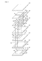
- FIG. 2 is an exploded perspective view of the multilayer balanced filter according to the first embodiment
- Fig. 3 is an external perspective view thereof.
- this multilayer balanced filter is configured as a stack containing a plurality of dielectric layers 101 to 106 each having predetermined electrode patterns formed thereon.
- this stack is constituted by a stack containing dielectric layers and electrode layers.
- An dielectric layer 103 has a first capacitor electrode 111 formed thereon.
- the first capacitor electrode 111 extends to the left side of the dielectric layer 103 via an electrode 144.
- a dielectric layer 102 has a ground electrode 110 formed thereon.
- the ground electrode 110 extends to the left and right sides of the dielectric layer 102 respectively via extension electrodes 140 and 141.
- the dielectric layer 101 has a second capacitor electrode 112 and a third capacitor electrode 113 formed thereon.
- the second capacitor electrode 112 extends to the right side of the dielectric layer 101 via an extension electrode 142.
- the third capacitor electrode 113 extends to the right side of the dielectric layer 101 via an extension electrode 143.
- a first capacitor is formed by the first capacitor electrode 111 and the ground electrode 110 facing each other.
- a second capacitor is formed by the second capacitor electrode 112 and the ground electrode 110 facing each other.
- a third capacitor is formed by the third capacitor electrode 113 and the ground electrode 110 facing each other.
- the dielectric layer 104 has a first straight line electrode 121 formed thereon.
- the dielectric layer 104 has a via electrode 132, which is a "vertical conduction electrode" according to the present invention, formed therethrough.
- a first end of the first straight line electrode 121 of the dielectric layer 104 is conductively connected to the first capacitor electrode 111 of the dielectric layer 103 using the via electrode 132.
- the dielectric layers 104 and 103 have a via electrode 131, which is the "vertical conduction electrode” according to the present invention, formed therethrough.
- a second end of the first straight line electrode 121 is conductively connected to the ground electrode 110 of the dielectric layer 102 using the via electrode 131.
- the first straight line electrode 121 and the via electrodes 131 and 132 constitute a first coil.
- the first coil has a winding axis perpendicular to the stacking direction, and forms a loop starting from the connection node of the via electrode 132 and the first capacitor electrode 111 and ending at the connection node of the via electrode 131 and the ground electrode 110.
- an LC parallel resonator is formed by the first coil and the first capacitor.
- the dielectric layer 104 has a portion 122 of a second coil and a portion 126 of a third coil formed thereon.
- the portion 122 of the second coil extends to right side of the dielectric layer 104 via an extension electrode 145.
- the portion 126 of the third coil extends to the right side of the dielectric layer 104 via an extension electrode 146.
- a dielectric layer 105 has an L-shaped portion 123 of the second coil, an inverted L-shaped portion 125 of the third coil, and a second straight line electrode 124 formed thereon.
- the portion 123 of the second coil is connected to a first end of the second straight line electrode 124, and the portion 125 of the third coil is connected to a second end of the second straight line electrode 124.
- the dielectric layer 105 has via electrodes 133 and 134, which are the "vertical conduction electrodes" according to the present invention, formed therethrough.
- the portion 122 of the second coil of the dielectric layer 104 is connected to the portion 122 of the second coil of the dielectric layer 105 using the via electrode 133.
- the portion 126 of the third coil of the dielectric layer 104 is connected to the portion 125 of the third coil of the dielectric layer 105 using the via electrode 134.
- the second coil having a helical shape is formed by the portion 122 of the second coil and the portion 123 of the second coil being conductively connected to each other.
- the third coil having a helical shape is formed by the portion 126 of the third coil and the portion 125 of the third coil being conductively connected to each other. These second and third coils are formed as loops with winding axes in the stacking direction.
- the electrodes of the first coil constituted by the first capacitor electrode 111, the via electrode 132, the first straight line electrode, the via electrode 131, and the ground electrode 110, are formed as a loop when viewed in a direction perpendicular to the stacking direction of the stack.
- the loop plane, having an opening, of this loop of the electrodes is perpendicular to the electrode layers.
- the loop planes of the second and third helical coils are parallel to the electrode layers.
- each of the second and third coils since the opening of the loop of the electrodes is arranged in the stacking direction, a magnetic field is generated which passes through the opening in the stacking direction. In this manner, since the direction of the magnetic field generated by the first coil is perpendicular to the directions of the magnetic fields generated by the second and third coils, the second and third coils have negligible coupling with the first coil.
- the first straight line electrode 121 and the second straight line electrode 124 which are arranged in parallel with each other, are electromagnetically (magnetically, in particular) coupled with each other.
- the two-dot chain line in Fig. 2 represents a projection of the first straight line electrode 121 on the dielectric layer 105.
- the gap GAP between the first straight line electrode 121 and the second straight line electrode 124 is set to a predetermined value in accordance with a desired amount of the coupling.
- the strength of coupling between the first and second straight line electrodes can be determined by the gap GAP.
- the dielectric layers 101 to 106 having various electrode patterns formed thereon are stacked to form a stack 10 as illustrated in Fig. 3 , and on two opposite sides (end surfaces) among the four sides of the stack 10, ground terminals 20, an unbalanced input terminal 21, balanced output terminals 22 and 23, and a non-connection terminal 24 are provided, thereby forming a multilayer balanced filter 11.
- the dimensions of the bottom surface and the height of the stack 10 are 1.6 mm ⁇ 0.8 mm and 0.5 mm.
- the dielectric portions of the dielectric layers 101 to 106 have relative dielectric constants within a range of 6 to 80. Specifically, the relative dielectric constants of the dielectric layers 102 and 103 that cause capacitance to be generated are equal to or above 20.
- LTCC low temperature co-fired ceramic
- LCP liquid crystal polymer
- polyimide polyimide
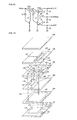
- Fig. 4 illustrates equivalent circuit diagrams of the multilayer balanced filter illustrated in Figs. 2 and 3 .
- Fig. 4(A) illustrates a relatively faithful equivalent circuit
- Fig. 4 (B) illustrates a simplified equivalent circuit thereof.
- an inductor L1 corresponds to the first coil constituted by the via electrodes 131 and 132 and the first straight line electrode 121 illustrated in Fig. 2 .
- an inductor L4 corresponds to the second straight line electrode 124 illustrated in Fig. 2 .
- an inductor L2 corresponds to the second coil constituted by the second coils 122 and 123 and the via electrode 133 illustrated in Fig. 2 .
- an inductor L3 corresponds to the third coil constituted by the third coils 125 and 126 and the via electrode 134 illustrated in Fig. 2 .
- a capacitor C1 is the first capacitor formed by the first capacitor electrode 111 and the ground electrode 110.
- a capacitor C2 is the second capacitor formed by the second capacitor electrode 112 and the ground electrode 110.
- a capacitor C3 is the third capacitor formed by the third capacitor electrode 113 and the ground electrode 110.
- the inductor L1 and the capacitor C1 illustrated in Fig. 4 constitute an LC parallel resonator.
- the midpoint of the inductor L4 is made to be a virtual ground
- half the inductor L4, the inductor L2, and the capacitor C2 constitute an LC parallel resonator.
- half the inductor L4, the inductor L3, and the capacitor C3 constitute an LC parallel resonator.
- the coupling coefficient M14 between the inductor L1 and the inductor L4 represents major coupling that enables the operation of a balanced-unbalanced converter.
- the coupling coefficient M12 between the inductor L1 and the inductor L2, and the coupling coefficient M13 between the inductor L1 and the inductor L2 represent parasitic coupling and are sufficiently smaller than the coupling coefficient M14.
- the equivalent circuit is simplified to that illustrated in Fig. 4 (B) .
- the inductors L2 and L3 are respectively connected in series to the two lines of the balanced output lines.
- the capacitors C2 and C3 are respectively connected between the ground and the two lines of the balanced output lines.
- the inductors L2 and L3, and the capacitors C2 and C3 operate as a circuit for impedance matching and conversion.
- an LC parallel resonator is formed by connecting the first straight line electrode 121 to the first capacitor electrode 111 and the ground electrode 110 using via electrodes, a resonator having a low conduction loss and a high Q value is formed. Hence, a low-loss passband characteristic is realized. Further, since the LC parallel resonator is provided on the unbalanced input side, the attenuation characteristic outside of the passband is improved.
- the impedance of the balanced output side can be set within a wide range using the inductances of the helical coils and the capacitances of the capacitors.
- the LC parallel resonator including the first coil is coupled with the LC parallel resonators including the second and third coils almost only by the magnetic coupling between the first straight line electrode and the second straight line electrode, adjustment of the coupling between resonators can be made only by adjusting the relative positional relationship of the first straight line electrode and the second straight line electrode. More specifically, the magnetic coupling between the first straight line electrode and the second straight line electrode can arbitrarily be adjusted by changing the respective positions thereof and the width of the dielectric layer, whereby optimal electromagnetic coupling and a desired passband width are obtained.
- the line width and the line length of the first straight line electrode 121 (inductor L1) illustrated in Fig. 2 corresponding to the inductors L1 and L4 illustrated in Fig. 4 are respectively made to be 0.1 mm and 0.5 mm.
- the capacitance of the capacitor C1 illustrated in Fig. 4 is made to be 13 pF.
- the resonance frequency is made to be 2.45 GHz
- the input impedance is made to be 50 ⁇ .
- the line width and line length of the second straight line electrode 124 (inductor L2) illustrated in Fig. 2 are respectively made to be 0.1 mm and 0.5 mm, and the gap between the first straight line electrode 121 and the second straight line electrode 124 is made to be 0.2 mm.
- the graphs illustrated in Fig. 5 each represent the S21 characteristic (attenuation characteristic) and S11 characteristic (reflection characteristic), which are S-parameter characteristics, when the inductances of the inductors L2 and L3 are changed.
- the vertical axis shows values in units of decibels with a reference value of 0 dB in all cases.
- Figs. 5 (A1), (A2), and (A3) illustrate changes in the characteristics when the capacitors C2 and C3 have a fixed value of 4 pF and the values of the inductors L2 and L3 are changed, under the conditions described above.
- Figs. 5 (B1), (B2), and (B3) illustrate changes in the characteristics when the inductors L2 and L3 have a fixed value of 0.5 nH and the values of the capacitors C2 and C3 are changed, under the conditions described above.
- Fig. 6 illustrates the S21 characteristic (attenuation characteristic) and S11 characteristic (reflection characteristic), which are S-parameter characteristics, when the gap GAP between the first straight line electrode 121 and the second straight line electrode 124 illustrated in Fig. 2 is changed.
- Figs. 6 (A), (B), and (C) illustrate examples in which the gaps are 0.2 mm, 0.18 mm in, and 0.16 mm, respectively.
- the value of GAP may be minus.
- the first straight line electrode 121 may be arranged in such a manner as to fully or at least partially overlap the second straight line electrode 124 in plan view.
- the coupling coefficient M14 illustrated in Fig. 4 (B) further increases and a wide-passband characteristic is obtained.
- Fig. 7 (A) illustrates the S11 characteristic (input port side reflection characteristic) and the S21 characteristic (insertion loss), which are S-parameter characteristics, of the differential mode of the balanced output ports P2-P3, and the S22 characteristic (output port side reflection loss).
- Fig. 7 (B) illustrates the S21 characteristic and the S31 characteristic where the horizontal and vertical axes have been magnified.
- Fig. 7 (C) illustrates the transmission characteristic of the same-phase component of the balanced output ports P2-P3.
- the vertical axis shows values in units of decibels with a reference value of 0 dB in all of Figs. 7 (A), (B), and (C) .
- Fig. 7 (A) illustrates the S11 characteristic (input port side reflection characteristic) and the S21 characteristic (insertion loss), which are S-parameter characteristics, of the differential mode of the balanced output ports P2-P3, and the S22 characteristic (output port side reflection loss).
- Fig. 7 (B) illustrates the S21 characteristic and
- Fig. 7 (D) it can be seen that, regarding the phase relationship between the balanced output ports P2 and P3, a phase difference of 180 degrees is kept for a wide range of frequencies, and a balanced signal is output across the balanced output ports P2 and P3 for a wide range of frequencies.
- FIG. 8 is an exploded perspective view of the multilayer balanced filter according to the second embodiment
- Fig. 9 is an external perspective view thereof.
- the differences from the first embodiment illustrated in Fig. 2 are the configurations of dielectric layers 101, 102, and 105.
- this multilayer balanced filter is configured as a stack containing a plurality of dielectric layers 101 to 106 each having predetermined electrode patterns formed thereon.
- this stack is constituted by a stack containing dielectric layers and electrode layers.
- the dielectric layer 103 has a first capacitor electrode 111 formed thereon.
- the first capacitor electrode 111 extends to the left side of the dielectric layer 103 via an extension electrode 144.
- the dielectric layer 102 has a ground electrode 110 formed thereon.
- the ground electrode 110 extends to the right side of the dielectric layer 102 via an extension electrode 141.
- the dielectric layer 101 has a second capacitor electrode 112, a third capacitor electrode 113, and a fourth capacitor electrode 114 formed thereon.
- the second capacitor electrode 112 extends to the right side of the dielectric layer 101 via an extension electrode 142.
- the third capacitor electrode 113 extends to the right side of the dielectric layer 101 via an extension electrode 143.
- the fourth capacitor electrode 114 extends to the left side of the dielectric layer 101 via an extension electrode 129.
- a first capacitor is formed by the first capacitor electrode 111 and the ground electrode 110 facing each other.
- a second capacitor is formed by the second capacitor electrode 112 and the ground electrode 110 facing each other.
- a third capacitor is formed by the third capacitor electrode 113 and the ground electrode 110 facing each other.
- a fourth capacitor is formed by the fourth capacitor electrode 114 and the ground electrode 110 facing each other.
- the dielectric layer 105 has an L-shaped portion 123 of a second coil, an inverted L-shaped portion 125 of a third coil, and a second straight line electrode 124 formed thereon.
- the portion 123 of the second coil is connected to a first end of the second straight line electrode 124, and the portion 125 of the third coil is connected to a second end of the second straight line electrode 124. Thereby, a loop pattern is formed.
- the middle of the second straight line electrode 124 extends to the left side of the dielectric layer 105 via an extension electrode 127.
- the configurations of the remaining dielectric layers are the same as those illustrated in Fig. 2 .
- the dielectric layers 101 to 106 having various electrode patterns formed thereon are stacked to form a stack 10 as illustrated in Fig. 9 , and on two opposite sides (end surfaces) among the four sides of the stack 10, a ground terminal 20, an unbalanced input terminal 21, balanced output terminals 22 and 23, a power feeding terminal 25, and a non-connection terminal 24 are provided, thereby forming a multilayer balanced filter 12.
- Fig. 10 is an equivalent circuit diagram of the multilayer balanced filter illustrated in Figs. 8 and 9 .
- a capacitor C4 is the fourth capacitor formed by the fourth capacitor electrode 114 and the ground electrode 110.
- the rest of the configuration is similar to that of the multilayer balanced filter according to the first embodiment.
- the fourth capacitor C4 is connected between the power feeding terminal 25 and the ground, and operates as a filter for suppressing high frequency noise. From the power feeding terminal 25, a bias voltage can be applied to an operational amplifier circuit (IC chip) connected to the balanced output terminals 22 and 23.
- IC chip operational amplifier circuit
- FIG. 11 is an exploded perspective view of the multilayer balanced filter according to the third embodiment
- Fig. 12 is an equivalent circuit diagram thereof.
- the difference from the multilayer balanced filter of the second embodiment illustrated in Fig. 8 is that a dielectric layer 107 is provided between a dielectric layer 103 and a dielectric layer 104.
- the dielectric layer 103 has a first capacitor electrode 111 and a fifth capacitor electrode 115 formed thereon.
- the fifth capacitor electrode 115 extends to the left side of the dielectric layer 103 via an electrode 144.
- a dielectric layer 102 has a ground electrode 110 formed thereon.
- the ground electrode 110 extends to the right side of the dielectric layer 102 via an extension electrode 141.
- a dielectric layer 101 has a second capacitor electrode 112, a third capacitor electrode 113, and a fourth capacitor electrode 114 formed thereon.
- the second capacitor electrode 112 extends to the right side of the dielectric layer 101 via an extension electrode 142.
- the third capacitor electrode 113 extends to the right side of the dielectric layer 101 via an extension electrode 143.
- the fourth capacitor electrode 114 extends to the left side of the dielectric layer 101 via an extension electrode 129.
- a first capacitor is formed by the first capacitor electrode 111 and the ground electrode 110 facing each other.
- a second capacitor is formed by the second capacitor electrode 112 and the ground electrode 110 facing each other.
- a third capacitor is formed by the third capacitor electrode 113 and the ground electrode 110 facing each other.
- a fourth capacitor is formed by the fourth capacitor electrode 114 and the ground electrode 110 facing each other.
- the dielectric layer 104 has a first straight line electrode 121 formed thereon.
- the dielectric layer 104 has a via electrode 132 formed therethrough. A first end of the first straight line electrode 121 of the dielectric layer 104 is conductively connected to the first capacitor electrode 111 of the dielectric layer 103 using the via electrode 132.
- the dielectric layers 104, 107, and 103 have a via electrode 131 formed therethrough.
- a second end of the first straight line electrode 121 is conductively connected to the ground electrode 110 of the dielectric layer 102 using the via electrode 131.
- the first straight line electrode 121 and the via electrodes 131 and 132 constitute a first coil. Hence, an LC parallel resonator is formed by the first coil and the first capacitor.
- the dielectric layer 104 has a third straight line electrode 128.
- the dielectric layer 104 has a via electrode 136.
- a first end of the third straight line electrode 128 of the dielectric layer 104 is conductively connected to the fifth capacitor electrode 115 using the via electrode 136.
- the dielectric layers 104, 107, and 103 have a via electrode 135 formed therethrough.
- a second end of the third straight line electrode 128 is conductively connected to the ground electrode 110 of the dielectric layer 102 using the via electrode 135.
- the third straight line electrode 128 and the via electrodes 135 and 136 constitute a fifth coil.
- an LC parallel resonator is formed by the fifth coil and the fifth capacitor.
- the dielectric layer 107 has a capacitor electrode 116 formed thereon in such a manner as to extend from the first capacitor electrode 111 of the dielectric layer 103 to the fifth capacitor electrode 115 in plan view.
- the configurations of a portion 122 of a second coil and a portion 126 of a third coil formed on the dielectric layer 104, and the configuration of a dielectric layer 105 are similar to those in the second embodiment illustrated in Fig. 8 .
- the dimensions of the bottom surface and the height of the stack containing the respective dielectric layers are 2.0 mm x 1.25 mm and 0.5 mm.
- Fig. 12 is an equivalent circuit diagram of the multilayer balanced filter illustrated in Fig. 11 .
- an inductor L5 corresponds to the fifth coil.
- a capacitor C5 corresponds to the fifth capacitor.
- a capacitor C12 corresponds to a capacitor formed by the first capacitor electrode 111, the fifth capacitor electrode 115, and the capacitor electrode 116. This configuration causes the two LC parallel resonators to be electromagnetically coupled with each other.
- the bandwidth can be increased, and the attenuation outside of a passband can also be increased.
- FIG. 13 is an exploded perspective view of the multilayer balanced filter according to the fourth embodiment.
- the difference from the multilayer balanced filter of the third embodiment illustrated in Fig. 11 is that a dielectric layer 107 does not exist between a dielectric layer 103 and a dielectric layer 104.
- the dielectric layers 104 and 103 have a via electrode 132 formed therethrough.
- a first end of a first straight line electrode 121 of the dielectric layer 104 is conductively connected to a ground electrode 110 of a dielectric layer 102 using the via electrode 132.
- the dielectric layer 104 has a via electrode 131 formed therethrough.
- a second end of the first straight line electrode 121 is conductively connected to a first capacitor electrode 111 of the dielectric layer 103 using the via electrode 131.
- the first straight line electrode 121 and the electrodes 131 and 132 constitute a first coil.
- the first coil and the first capacitor constitute an LC resonator.
- the dielectric layer 104 has a third straight line electrode 128 formed thereon.
- the dielectric layer 104 has a via electrode 136 formed therethrough.
- a first end of the third straight line electrode 128 of the dielectric layer 104 is conductively connected to the fifth capacitor electrode 115 of the dielectric layer 103 using the via electrode 136.
- the dielectric layers 104 and 103 have a via electrode 135 formed therethrough.
- a second end of the third straight line electrode 128 is connected to the ground electrode 110 of the dielectric layer 102 using the via electrode 135.
- the third straight line electrode 128 and the via electrodes 135 and 136 constitute a fifth coil.
- the fifth coil and the fifth capacitor constitute an LC parallel resonator.
- the configurations of a portion 122 of a second coil and a portion 126 of a third coil formed on the dielectric layer 104, and the configuration of a dielectric layer 105 are similar to those in the second embodiment illustrated in Fig. 8 .
- the equivalent circuit diagram of the multilayer balanced filter illustrated in Fig. 13 is the same as that illustrated in Fig. 12 .
- the two LC parallel resonators are capacitively coupled without a capacitor electrode corresponding to a capacitor C12 which causes the two LC parallel resonators to be coupled with each other.
- LC parallel resonators in two stages are provided in the third and fourth embodiments, LC parallel resonators may be provided in three or more stages in a similar way.
- FIG. 14 is an exploded perspective view of the multilayer balanced filter according to the fifth embodiment.
- the difference from the multilayer balanced filter of the first embodiment illustrated in Fig. 2 is the shape of a second straight line electrode 124.
- a step is formed in the middle of the second straight line electrode 124, whereby the distances from a first half and a second half of the second straight line electrode 124 to a first straight line electrode 121 are made to be different from each other.
- the balance of the balanced output can appropriately be determined.
- the second and third coils which are circuits on the balanced side, can be configured in such a manner as to be line-symmetric; however, in the circuits on the unbalanced side, strictly speaking, a first capacitor electrode 111 and via electrodes 131 and 132 cannot be made to be line-symmetric. Hence, when the balanced output becomes unbalanced, it is effective to realize balance by employing the shape of the second straight line electrode as illustrated in Fig. 14 .
- the distances from a first half and a second half of the first straight line electrode 121 to the second straight line electrode 124 may be made to be different from each other.
- the balance of the balanced output may be realized by making the first straight line electrode 121 or the second straight line electrode 124 have a line width which is not uniform but differs between a first half and a second half thereof.
Landscapes
- Engineering & Computer Science (AREA)
- Power Engineering (AREA)
- Filters And Equalizers (AREA)
- Control Of Motors That Do Not Use Commutators (AREA)
- Coils Or Transformers For Communication (AREA)
Abstract
Description
- The present invention relates to a multilayer balanced filter including a stack containing a plurality of dielectric layers and electrode layers.
- A typical conventional band pass filter whose size and cost can be easily reduced is formed by providing a plurality of LC resonance circuits within a stack containing dielectric layers and electrode layers.
Such a multilayer band pass filter is disclosed in Patent Document 1. - The configuration of a multilayer band pass filter disclosed in Patent Document 1 is described with reference to
Fig. 1 .
Fig. 1 is a circuit diagram of the multilayer band pass filter disclosed in Patent Document 1. The multilayer band pass filter 1 includes an unbalanced input terminal 2,balanced output terminals 3A and 3B, and a band pass filter portion 4 provided between the unbalanced input terminal 2 and thebalanced output terminals 3A and 3B. The band pass filter portion 4 is constituted by threeresonators 40 arranged in a line, where each oscillator is a 1/2-wavelength resonator 40 whose both ends are open. Theresonator 40 arranged at a position closest to the unbalanced input terminal 2 among the threeresonators 40 is an input resonator 40I. The input resonator 40I is directly connected to the unbalanced input terminal 2. Theresonator 40 arranged at a position closest to thebalanced output terminals 3A and 3B is a balanced output 1/2-wavelength resonator 41A. The balanced output 1/2-wavelength resonator 41A is connected to thebalanced output terminals 3A and 3B. The input resonator 40I is electromagnetically coupled with anintermediate resonator 40M, and theintermediate resonator 40M is also electromagnetically coupled with the balanced output 1/2-wavelength resonator 41A. The open ends of the threeresonators 40 are connected to the ground by capacitors C. -
- [Patent Document 1] Japanese Unexamined Patent Application Publication No.
2005-45447 - In the multilayer band pass filter disclosed in Patent Document 1, a balanced-unbalanced conversion function and filter characteristics are realized by arranging a plurality of λ/2 resonators having open ends on the same surface of a substrate and thereby coupling the resonators with one another.
- In the case of a filter having a balanced-unbalanced conversion function, the balanced terminals thereof are generally often connected to an IC which performs balanced input/output of signals. In this case, impedance conversion is required between the unbalanced terminal and the balanced terminals. However, the structure described in Patent Document 1 does not allow for easy design and adjustment for appropriate impedance conversion between these two types of terminals.
- Further, even when a circuit for impedance conversion is provided, an additional area corresponding to the impedance conversion circuit portion is required, thereby preventing general reduction in size.
- Hence, an object of the present invention is to solve the above problems and provide a multilayer balanced filter whose size can be easily reduced and which can realize specified impedance conversion between the input and output thereof.
- To solve the above-described problems, a multilayer balanced filter according to the present invention is configured as follows.
- (1) A multilayer balanced filter configured as a stack including a plurality of electrode layers, a plurality of dielectric layers provided among the electrode layers, and vertical conduction electrodes arranged in a stacking direction of the electrode layers,
wherein the plurality of electrodes includes a first straight line electrode and a second straight line electrode, each having a substantially straight-line shape, arranged in parallel with each other, and the first straight line electrode and the vertical conduction electrodes connected to both ends of the first straight line electrode constitute a first coil,
wherein the plurality of electrode layers include a ground electrode and a first capacitor electrode, a second capacitor electrode, and a third capacitor electrode, each facing the ground electrode, and the ground electrode and the first capacitor electrode constitute a first capacitor, the ground electrode and the second capacitor electrode constitute a second capacitor, and the ground electrode and the third capacitor electrode constitute a third capacitor, - Using this configuration, balanced-unbalanced conversion is performed by using the coupling between the first straight line electrode and the second straight line electrode, and impedance conversion is performed by the second coil, the third coil, the second capacitor, and the third capacitor. Further, a plurality of LC parallel resonators constituted by the first to third capacitors, the first to third coils, and the second straight line electrode function as band pass filters.
- (2) Typically, the first straight line electrode and the second straight line electrode are formed on different layers.
This allows the strength of coupling between the first straight line electrode and the second straight line electrode to be increased. In addition, the relative positions of the first straight line electrode and the second straight line electrode can be easily changed, whereby the freedom of design regarding the strength of coupling is increased. Hence, a desired pass band characteristic is obtained by setting of the electromagnetic coupling between the LC parallel resonator on the unbalanced side and the second and thirds coils on the balanced side. - (3) The first straight line electrode and the second straight line electrode may be arranged in such a manner that one overlaps the other at least partially in plan view.
This structure allows the strength of coupling between the first straight line electrode and the second straight line electrode to be increased and the width of the passband to be increased. - (4) The plurality of electrode layers may include a power feeding terminal extension electrode connected to the second straight line electrode.
This allows a dc source voltage to be applied to an IC connected to the balanced terminals. Specifically, by forming the first straight line electrode and the second straight line electrode on different layers, and forming the power feeding terminal extension electrode on the layer having the second straight line electrode formed thereon, a power feeding terminal for dc feeding can be easily provided without using a special dielectric layer. - (5) The ground electrode is preferably arranged between a group of the second and third capacitor electrodes and a group of the second and third coils.
This makes it possible to design the second and third capacitor electrodes and design the second and third coils separately and hence easily. In addition, the ground electrode can be commonly used among the first, second, and third capacitors, thereby realizing a decrease in the number of ground electrodes, leading to a lower height of the stack. - (6) Each of the second coil and the third coil may be constituted by coil portions respectively formed on a plurality of the electrode layers and the vertical conduction electrode, and the second and third coils may have opposite winding directions and helical shapes, and may substantially be line-symmetrically arranged.
- This structure allows the inductances of the second and third coils to be set within a wide range. Hence, the impedance on the balanced side can be determined over a wide range. In addition, by making the coils have opposite winding directions and substantially be arranged line-symmetrically, the difference in amplitude between the balanced output terminals can be decreased.
- According to the present invention, a multilayer balanced filter can be formed that is small in size and realizes predetermined impedance conversion between the input and output thereof.
-
- [
Fig. 1] Fig. 1 is a circuit diagram of the multilayer band pass filter disclosed in Patent Document 1. - [
Fig. 2] Fig. 2 is an exploded perspective view of a multilayer balanced filter according to a first embodiment. - [
Fig. 3] Fig. 3 is an external perspective view the multilayer balanced filter according to the first embodiment. - [
Fig. 4] Fig. 4 illustrates equivalent circuit diagrams of the multilayer balanced filter illustrated inFigs. 2 and 3 . - [
Fig. 5] Fig. 5 illustrates the relationships among output impedances, attenuation characteristics, and reflection characteristics for settings of inductors L2 and L2, capacitors C2 and C3 on the balanced side. - [
Fig. 6] Fig. 6 illustrates attenuation characteristics and reflection characteristics when the gap GAP between a firststraight line electrode 121 and a secondstraight line electrode 124 is changed. - [
Fig. 7] Fig. 7 illustrates various characteristics for an input impedance Zin = 50 Ω and an output impedance Zout = 24 + j55 Ω realized by the settings of C1, L1, C2, C3, L2, and L3. - [
Fig. 8] Fig. 8 is an exploded perspective view of a multilayer balanced filter according to a second embodiment. - [
Fig. 9] Fig. 9 is an external perspective view of the multilayer balanced filter according to the second embodiment. - [
Fig. 10] Fig. 10 is an equivalent circuit diagram of the multilayer balanced filter according to the second embodiment. - [
Fig. 11] Fig. 11 is an exploded perspective view of a multilayer balanced filter according to a third embodiment. - [
Fig. 12] Fig. 12 an equivalent circuit diagram of the multilayer balanced filter according to the third embodiment. - [
Fig. 13] Fig. 13 is an exploded perspective view of a multilayer balanced filter according to a fourth embodiment. - [
Fig. 14] Fig. 14 is an exploded perspective view of a multilayer balanced filter according to a fifth embodiment. - A multilayer balanced filter according to a first embodiment will be described with reference to
Figs. 2 to 7 .
Fig. 2 is an exploded perspective view of the multilayer balanced filter according to the first embodiment, andFig. 3 is an external perspective view thereof. - Referring to
Fig. 2 , this multilayer balanced filter is configured as a stack containing a plurality ofdielectric layers 101 to 106 each having predetermined electrode patterns formed thereon. Hence, this stack is constituted by a stack containing dielectric layers and electrode layers. - An
dielectric layer 103 has afirst capacitor electrode 111 formed thereon. Thefirst capacitor electrode 111 extends to the left side of thedielectric layer 103 via anelectrode 144. Adielectric layer 102 has aground electrode 110 formed thereon. Theground electrode 110 extends to the left and right sides of thedielectric layer 102 respectively viaextension electrodes dielectric layer 101 has asecond capacitor electrode 112 and athird capacitor electrode 113 formed thereon. Thesecond capacitor electrode 112 extends to the right side of thedielectric layer 101 via anextension electrode 142. Thethird capacitor electrode 113 extends to the right side of thedielectric layer 101 via anextension electrode 143. - A first capacitor is formed by the
first capacitor electrode 111 and theground electrode 110 facing each other. A second capacitor is formed by thesecond capacitor electrode 112 and theground electrode 110 facing each other. Similarly, a third capacitor is formed by thethird capacitor electrode 113 and theground electrode 110 facing each other. - The
dielectric layer 104 has a firststraight line electrode 121 formed thereon.
Thedielectric layer 104 has a viaelectrode 132, which is a "vertical conduction electrode" according to the present invention, formed therethrough. A first end of the firststraight line electrode 121 of thedielectric layer 104 is conductively connected to thefirst capacitor electrode 111 of thedielectric layer 103 using the viaelectrode 132. - The
dielectric layers electrode 131, which is the "vertical conduction electrode" according to the present invention, formed therethrough. A second end of the firststraight line electrode 121 is conductively connected to theground electrode 110 of thedielectric layer 102 using the viaelectrode 131.
The firststraight line electrode 121 and the viaelectrodes electrode 132 and thefirst capacitor electrode 111 and ending at the connection node of the viaelectrode 131 and theground electrode 110. Hence, an LC parallel resonator is formed by the first coil and the first capacitor. - The
dielectric layer 104 has aportion 122 of a second coil and aportion 126 of a third coil formed thereon. Theportion 122 of the second coil extends to right side of thedielectric layer 104 via anextension electrode 145. Theportion 126 of the third coil extends to the right side of thedielectric layer 104 via anextension electrode 146. - A
dielectric layer 105 has an L-shapedportion 123 of the second coil, an inverted L-shapedportion 125 of the third coil, and a secondstraight line electrode 124 formed thereon. Theportion 123 of the second coil is connected to a first end of the secondstraight line electrode 124, and theportion 125 of the third coil is connected to a second end of the secondstraight line electrode 124. Thereby, a "C"-shaped loop pattern in plan view when viewed in a direction perpendicular to the main surface of the dielectric layer is formed. - The
dielectric layer 105 has viaelectrodes portion 122 of the second coil of thedielectric layer 104 is connected to theportion 122 of the second coil of thedielectric layer 105 using the viaelectrode 133. Theportion 126 of the third coil of thedielectric layer 104 is connected to theportion 125 of the third coil of thedielectric layer 105 using the viaelectrode 134. Hence, the second coil having a helical shape is formed by theportion 122 of the second coil and theportion 123 of the second coil being conductively connected to each other. Similarly, the third coil having a helical shape is formed by theportion 126 of the third coil and theportion 125 of the third coil being conductively connected to each other. These second and third coils are formed as loops with winding axes in the stacking direction. - The electrodes of the first coil constituted by the
first capacitor electrode 111, the viaelectrode 132, the first straight line electrode, the viaelectrode 131, and theground electrode 110, are formed as a loop when viewed in a direction perpendicular to the stacking direction of the stack. The loop plane, having an opening, of this loop of the electrodes is perpendicular to the electrode layers. On the other hand, the loop planes of the second and third helical coils are parallel to the electrode layers. When currents flow through the first to third coils, magnetic fields are generated around the electrodes. Since the first coil is formed in the stacking direction of the stack as a loop of electrodes having an opening, a magnetic field is generated which passes through the opening in a direction perpendicular to the stacking direction. On the other hand, in each of the second and third coils, since the opening of the loop of the electrodes is arranged in the stacking direction, a magnetic field is generated which passes through the opening in the stacking direction. In this manner, since the direction of the magnetic field generated by the first coil is perpendicular to the directions of the magnetic fields generated by the second and third coils, the second and third coils have negligible coupling with the first coil.
The firststraight line electrode 121 and the secondstraight line electrode 124, which are arranged in parallel with each other, are electromagnetically (magnetically, in particular) coupled with each other. The two-dot chain line inFig. 2 represents a projection of the firststraight line electrode 121 on thedielectric layer 105. The gap GAP between the firststraight line electrode 121 and the secondstraight line electrode 124 is set to a predetermined value in accordance with a desired amount of the coupling. - As will be described later, the strength of coupling between the first and second straight line electrodes can be determined by the gap GAP.
- The
dielectric layers 101 to 106 having various electrode patterns formed thereon are stacked to form astack 10 as illustrated inFig. 3 , and on two opposite sides (end surfaces) among the four sides of thestack 10,ground terminals 20, anunbalanced input terminal 21,balanced output terminals balanced filter 11. The dimensions of the bottom surface and the height of thestack 10 are 1.6 mm × 0.8 mm and 0.5 mm. - The dielectric portions of the
dielectric layers 101 to 106 have relative dielectric constants within a range of 6 to 80. Specifically, the relative dielectric constants of thedielectric layers -
Fig. 4 illustrates equivalent circuit diagrams of the multilayer balanced filter illustrated inFigs. 2 and 3 .Fig. 4(A) illustrates a relatively faithful equivalent circuit, andFig. 4 (B) illustrates a simplified equivalent circuit thereof. Referring toFig. 4 , an inductor L1 corresponds to the first coil constituted by the viaelectrodes straight line electrode 121 illustrated inFig. 2 . Referring toFig. 4 , an inductor L4 corresponds to the secondstraight line electrode 124 illustrated inFig. 2 . Referring toFig. 4 , an inductor L2 corresponds to the second coil constituted by thesecond coils electrode 133 illustrated inFig. 2 . Similarly, an inductor L3 corresponds to the third coil constituted by thethird coils electrode 134 illustrated inFig. 2 . - Referring to
Fig. 4 , a capacitor C1 is the first capacitor formed by thefirst capacitor electrode 111 and theground electrode 110. Similarly, a capacitor C2 is the second capacitor formed by thesecond capacitor electrode 112 and theground electrode 110. Similarly, a capacitor C3 is the third capacitor formed by thethird capacitor electrode 113 and theground electrode 110.
The inductor L1 and the capacitor C1 illustrated inFig. 4 constitute an LC parallel resonator. When the midpoint of the inductor L4 is made to be a virtual ground, half the inductor L4, the inductor L2, and the capacitor C2 constitute an LC parallel resonator. Similarly, half the inductor L4, the inductor L3, and the capacitor C3 constitute an LC parallel resonator. - The coupling coefficient M14 between the inductor L1 and the inductor L4 represents major coupling that enables the operation of a balanced-unbalanced converter. The coupling coefficient M12 between the inductor L1 and the inductor L2, and the coupling coefficient M13 between the inductor L1 and the inductor L2 represent parasitic coupling and are sufficiently smaller than the coupling coefficient M14. Hence, the equivalent circuit is simplified to that illustrated in
Fig. 4 (B) . Referring toFig. 4(B) , the inductors L2 and L3 are respectively connected in series to the two lines of the balanced output lines. The capacitors C2 and C3 are respectively connected between the ground and the two lines of the balanced output lines. The inductors L2 and L3, and the capacitors C2 and C3 operate as a circuit for impedance matching and conversion. - According to the first embodiment of the present invention, since an LC parallel resonator is formed by connecting the first
straight line electrode 121 to thefirst capacitor electrode 111 and theground electrode 110 using via electrodes, a resonator having a low conduction loss and a high Q value is formed. Hence, a low-loss passband characteristic is realized. Further, since the LC parallel resonator is provided on the unbalanced input side, the attenuation characteristic outside of the passband is improved. In addition, since the balanced output side is formed using helical coils, and a capacitor is connected to an end of each of the helical coils, the impedance of the balanced output side can be set within a wide range using the inductances of the helical coils and the capacitances of the capacitors. Further, since the LC parallel resonator including the first coil is coupled with the LC parallel resonators including the second and third coils almost only by the magnetic coupling between the first straight line electrode and the second straight line electrode, adjustment of the coupling between resonators can be made only by adjusting the relative positional relationship of the first straight line electrode and the second straight line electrode. More specifically, the magnetic coupling between the first straight line electrode and the second straight line electrode can arbitrarily be adjusted by changing the respective positions thereof and the width of the dielectric layer, whereby optimal electromagnetic coupling and a desired passband width are obtained. - A method of designing the impedance for obtaining appropriate balanced-unbalanced conversion and band pass filter characteristics will now be described with reference to
Figs. 5 to 7 . First, the line width and the line length of the first straight line electrode 121 (inductor L1) illustrated inFig. 2 corresponding to the inductors L1 and L4 illustrated inFig. 4 are respectively made to be 0.1 mm and 0.5 mm. The capacitance of the capacitor C1 illustrated inFig. 4 is made to be 13 pF. Thereby, the resonance frequency is made to be 2.45 GHz, and the input impedance is made to be 50 Ω. - The line width and line length of the second straight line electrode 124 (inductor L2) illustrated in
Fig. 2 are respectively made to be 0.1 mm and 0.5 mm, and the gap between the firststraight line electrode 121 and the secondstraight line electrode 124 is made to be 0.2 mm. - The graphs illustrated in
Fig. 5 each represent the S21 characteristic (attenuation characteristic) and S11 characteristic (reflection characteristic), which are S-parameter characteristics, when the inductances of the inductors L2 and L3 are changed. The vertical axis shows values in units of decibels with a reference value of 0 dB in all cases. -
Figs. 5 (A1), (A2), and (A3) illustrate changes in the characteristics when the capacitors C2 and C3 have a fixed value of 4 pF and the values of the inductors L2 and L3 are changed, under the conditions described above.Fig. 5 (A1) corresponds to the case where L2 and L3 = 0.5 nH,Fig. 5 (A2) corresponds to the case where L2 and L3 = 0.6 nH, andFig. 5 (A3) corresponds to the case where L2 and L3 = 0.7 nH. - On the other hand,
Figs. 5 (B1), (B2), and (B3) illustrate changes in the characteristics when the inductors L2 and L3 have a fixed value of 0.5 nH and the values of the capacitors C2 and C3 are changed, under the conditions described above.Fig. 5 (B1) corresponds to the case where C2 and C3 = 3.5 pF,Fig. 5 (B2) corresponds to the case where C2 and C3 = 4.5 pF, andFig. 5 (B3) corresponds to the case where C2 and C3 = 5 pF. - The relationship between the circuit constants of the impedance matching circuit portion and the output impedance Zout is as follows:
- (A1) L2, L3 = 0.5 nH Output impedance Zout = 20 + j50 Ω
- (A2) L2, L3 = 0.6 nH Output impedance Zout = 40 + j80 Ω
- (A3) L2, L3 = 0.7 nH Output impedance Zout = 80 + j120 Ω
- (B1) C2, C3 = 3.5 pF Output impedance Zout = 15 + j45 Ω
- (B2) C2, C3 = 4.5 pF Output impedance Zout = 35 + j65 Ω
- (B3) C2, C3 = 5 pF Output impedance Zout = 55 + j75 Ω
It can be seen from these that the output impedance increases as the inductances of the inductors L2 and L3 increase, and the output impedance increases as the capacitances of the capacitors C2 and C3 increase. -
Fig. 6 illustrates the S21 characteristic (attenuation characteristic) and S11 characteristic (reflection characteristic), which are S-parameter characteristics, when the gap GAP between the firststraight line electrode 121 and the secondstraight line electrode 124 illustrated inFig. 2 is changed. The vertical axis shows values in units of decibels with a reference value of 0 dB in all cases. In all cases, C1 = 13 pF, C2 and C3 = 4pF, L2 and L3 = 0.5 nH.Figs. 6 (A), (B), and (C) illustrate examples in which the gaps are 0.2 mm, 0.18 mm in, and 0.16 mm, respectively. - As can be clearly seen from
Fig. 6 , the smaller the gap GAP between the firststraight line electrode 121 and the secondstraight line electrode 124, the wider the passband due to the increase in the coupling coefficient M14 illustrated inFig. 4 (B) . - Note that the value of GAP may be minus. In other words, the first
straight line electrode 121 may be arranged in such a manner as to fully or at least partially overlap the secondstraight line electrode 124 in plan view. Thereby, the coupling coefficient M14 illustrated inFig. 4 (B) further increases and a wide-passband characteristic is obtained. -
Fig. 7 illustrates various characteristics for the input impedance Zin = 50 Ω and the output impedance Zout = 25 + j55 Ω realized by the above-described settings of C1, L1, C2, C3, L2, and L3. -
Fig. 7 (A) illustrates the S11 characteristic (input port side reflection characteristic) and the S21 characteristic (insertion loss), which are S-parameter characteristics, of the differential mode of the balanced output ports P2-P3, and the S22 characteristic (output port side reflection loss).Fig. 7 (B) illustrates the S21 characteristic and the S31 characteristic where the horizontal and vertical axes have been magnified.Fig. 7 (C) illustrates the transmission characteristic of the same-phase component of the balanced output ports P2-P3. The vertical axis shows values in units of decibels with a reference value of 0 dB in all ofFigs. 7 (A), (B), and (C) . InFig. 7 (D) , "S21" illustrates the phase between the ports P1 and P2, and "S31" illustrates the phase between the ports P1 and P3.
The respective port numbers correspond to the ports P1, P2, and P3 illustrated inFig. 4(B) . - As illustrated in
Fig. 7 (A) , it can be seen that the reflection losses S11 and S22 in a used frequency band 2.45 GHz are small, and impedance matching is realized at the unbalanced input port P1 and the balanced output ports P2 and P3. - As illustrated in
Fig. 7 (B) , it can be seen that the reflection losses S21 and S31 in the used frequency band 2.45 GHz are the same, and the output balance at the balanced output ports P2 and P3 is realized. - As illustrated in
Fig. 7 (C) , it can be seen that the common mode output of the balanced output ports P2 and P3 is -20 dB or less, showing that the output at the balanced output ports P2 and P3 is sufficiently balanced. - Further, as illustrated in
Fig. 7 (D) , it can be seen that, regarding the phase relationship between the balanced output ports P2 and P3, a phase difference of 180 degrees is kept for a wide range of frequencies, and a balanced signal is output across the balanced output ports P2 and P3 for a wide range of frequencies. - A multilayer balanced filter according to a second embodiment will be described with reference to
Figs. 8 to 10 .
Fig. 8 is an exploded perspective view of the multilayer balanced filter according to the second embodiment, andFig. 9 is an external perspective view thereof. The differences from the first embodiment illustrated inFig. 2 are the configurations ofdielectric layers - Referring to
Fig. 8 , this multilayer balanced filter is configured as a stack containing a plurality ofdielectric layers 101 to 106 each having predetermined electrode patterns formed thereon. Hence, this stack is constituted by a stack containing dielectric layers and electrode layers. - The
dielectric layer 103 has afirst capacitor electrode 111 formed thereon. Thefirst capacitor electrode 111 extends to the left side of thedielectric layer 103 via anextension electrode 144. Thedielectric layer 102 has aground electrode 110 formed thereon. Theground electrode 110 extends to the right side of thedielectric layer 102 via anextension electrode 141. Thedielectric layer 101 has asecond capacitor electrode 112, athird capacitor electrode 113, and afourth capacitor electrode 114 formed thereon. Thesecond capacitor electrode 112 extends to the right side of thedielectric layer 101 via anextension electrode 142. Thethird capacitor electrode 113 extends to the right side of thedielectric layer 101 via anextension electrode 143. Thefourth capacitor electrode 114 extends to the left side of thedielectric layer 101 via anextension electrode 129. - A first capacitor is formed by the
first capacitor electrode 111 and theground electrode 110 facing each other. A second capacitor is formed by thesecond capacitor electrode 112 and theground electrode 110 facing each other. Similarly, a third capacitor is formed by thethird capacitor electrode 113 and theground electrode 110 facing each other. In addition, a fourth capacitor is formed by thefourth capacitor electrode 114 and theground electrode 110 facing each other. - The
dielectric layer 105 has an L-shapedportion 123 of a second coil, an inverted L-shapedportion 125 of a third coil, and a secondstraight line electrode 124 formed thereon. Theportion 123 of the second coil is connected to a first end of the secondstraight line electrode 124, and theportion 125 of the third coil is connected to a second end of the secondstraight line electrode 124. Thereby, a loop pattern is formed. - On the
dielectric layer 105, the middle of the secondstraight line electrode 124 extends to the left side of thedielectric layer 105 via anextension electrode 127.
The configurations of the remaining dielectric layers are the same as those illustrated inFig. 2 . - The
dielectric layers 101 to 106 having various electrode patterns formed thereon are stacked to form astack 10 as illustrated inFig. 9 , and on two opposite sides (end surfaces) among the four sides of thestack 10, aground terminal 20, anunbalanced input terminal 21,balanced output terminals power feeding terminal 25, and a non-connection terminal 24 are provided, thereby forming a multilayerbalanced filter 12. -
Fig. 10 is an equivalent circuit diagram of the multilayer balanced filter illustrated inFigs. 8 and 9 . InFig. 10 , a capacitor C4 is the fourth capacitor formed by thefourth capacitor electrode 114 and theground electrode 110. The rest of the configuration is similar to that of the multilayer balanced filter according to the first embodiment. - The fourth capacitor C4 is connected between the
power feeding terminal 25 and the ground, and operates as a filter for suppressing high frequency noise. From thepower feeding terminal 25, a bias voltage can be applied to an operational amplifier circuit (IC chip) connected to thebalanced output terminals - A multilayer balanced filter according to a third embodiment will be described with reference to
Figs. 11 and12 .
Fig. 11 is an exploded perspective view of the multilayer balanced filter according to the third embodiment, andFig. 12 is an equivalent circuit diagram thereof. The difference from the multilayer balanced filter of the second embodiment illustrated inFig. 8 is that adielectric layer 107 is provided between adielectric layer 103 and adielectric layer 104. - The
dielectric layer 103 has afirst capacitor electrode 111 and afifth capacitor electrode 115 formed thereon. Thefifth capacitor electrode 115 extends to the left side of thedielectric layer 103 via anelectrode 144.
Adielectric layer 102 has aground electrode 110 formed thereon. Theground electrode 110 extends to the right side of thedielectric layer 102 via anextension electrode 141.
Adielectric layer 101 has asecond capacitor electrode 112, athird capacitor electrode 113, and afourth capacitor electrode 114 formed thereon. Thesecond capacitor electrode 112 extends to the right side of thedielectric layer 101 via anextension electrode 142. Thethird capacitor electrode 113 extends to the right side of thedielectric layer 101 via anextension electrode 143. Thefourth capacitor electrode 114 extends to the left side of thedielectric layer 101 via anextension electrode 129. - A first capacitor is formed by the
first capacitor electrode 111 and theground electrode 110 facing each other. A second capacitor is formed by thesecond capacitor electrode 112 and theground electrode 110 facing each other. Similarly, a third capacitor is formed by thethird capacitor electrode 113 and theground electrode 110 facing each other. In addition, a fourth capacitor is formed by thefourth capacitor electrode 114 and theground electrode 110 facing each other. - The
dielectric layer 104 has a firststraight line electrode 121 formed thereon.
Thedielectric layer 104 has a viaelectrode 132 formed therethrough. A first end of the firststraight line electrode 121 of thedielectric layer 104 is conductively connected to thefirst capacitor electrode 111 of thedielectric layer 103 using the viaelectrode 132. - The
dielectric layers electrode 131 formed therethrough. A second end of the firststraight line electrode 121 is conductively connected to theground electrode 110 of thedielectric layer 102 using the viaelectrode 131.
The firststraight line electrode 121 and the viaelectrodes - The
dielectric layer 104 has a thirdstraight line electrode 128.
Thedielectric layer 104 has a viaelectrode 136. A first end of the thirdstraight line electrode 128 of thedielectric layer 104 is conductively connected to thefifth capacitor electrode 115 using the viaelectrode 136. - The
dielectric layers electrode 135 formed therethrough. A second end of the thirdstraight line electrode 128 is conductively connected to theground electrode 110 of thedielectric layer 102 using the viaelectrode 135.
The thirdstraight line electrode 128 and the viaelectrodes - The
dielectric layer 107 has acapacitor electrode 116 formed thereon in such a manner as to extend from thefirst capacitor electrode 111 of thedielectric layer 103 to thefifth capacitor electrode 115 in plan view. - The configurations of a
portion 122 of a second coil and aportion 126 of a third coil formed on thedielectric layer 104, and the configuration of adielectric layer 105 are similar to those in the second embodiment illustrated inFig. 8 .
The dimensions of the bottom surface and the height of the stack containing the respective dielectric layers are 2.0 mm x 1.25 mm and 0.5 mm. -
Fig. 12 is an equivalent circuit diagram of the multilayer balanced filter illustrated inFig. 11 . Referring toFig. 12 , an inductor L5 corresponds to the fifth coil. A capacitor C5 corresponds to the fifth capacitor. A capacitor C12 corresponds to a capacitor formed by thefirst capacitor electrode 111, thefifth capacitor electrode 115, and thecapacitor electrode 116. This configuration causes the two LC parallel resonators to be electromagnetically coupled with each other. - By providing the LC parallel resonators in two stages in this manner, the bandwidth can be increased, and the attenuation outside of a passband can also be increased.
- A multilayer balanced filter according to a fourth embodiment will be described with reference to
Fig. 13 .
Fig. 13 is an exploded perspective view of the multilayer balanced filter according to the fourth embodiment. The difference from the multilayer balanced filter of the third embodiment illustrated inFig. 11 is that adielectric layer 107 does not exist between adielectric layer 103 and adielectric layer 104. - The
dielectric layers electrode 132 formed therethrough. A first end of a firststraight line electrode 121 of thedielectric layer 104 is conductively connected to aground electrode 110 of adielectric layer 102 using the viaelectrode 132. - The
dielectric layer 104 has a viaelectrode 131 formed therethrough. A second end of the firststraight line electrode 121 is conductively connected to afirst capacitor electrode 111 of thedielectric layer 103 using the viaelectrode 131.
The firststraight line electrode 121 and theelectrodes - The
dielectric layer 104 has a thirdstraight line electrode 128 formed thereon.
Thedielectric layer 104 has a viaelectrode 136 formed therethrough. A first end of the thirdstraight line electrode 128 of thedielectric layer 104 is conductively connected to thefifth capacitor electrode 115 of thedielectric layer 103 using the viaelectrode 136. - The
dielectric layers electrode 135 formed therethrough. A second end of the thirdstraight line electrode 128 is connected to theground electrode 110 of thedielectric layer 102 using the viaelectrode 135.
The thirdstraight line electrode 128 and the viaelectrodes - The configurations of a
portion 122 of a second coil and aportion 126 of a third coil formed on thedielectric layer 104, and the configuration of adielectric layer 105 are similar to those in the second embodiment illustrated inFig. 8 . - The equivalent circuit diagram of the multilayer balanced filter illustrated in
Fig. 13 is the same as that illustrated inFig. 12 . In the example illustrated inFig. 13 , since the winding directions of the first and fifth coils are opposite to each other, the two LC parallel resonators are capacitively coupled without a capacitor electrode corresponding to a capacitor C12 which causes the two LC parallel resonators to be coupled with each other. - In this manner, since a coupling capacitor is not required, there is no variation in coupling that depends on the processing accuracy, whereby stable characteristics are realized. In addition, since the number of dielectric layers is decreased, the height is reduced.
- Although LC parallel resonators in two stages are provided in the third and fourth embodiments, LC parallel resonators may be provided in three or more stages in a similar way.
- A multilayer balanced filter according to a fifth embodiment will be described with reference to
Fig. 14 .
Fig. 14 is an exploded perspective view of the multilayer balanced filter according to the fifth embodiment. The difference from the multilayer balanced filter of the first embodiment illustrated inFig. 2 is the shape of a secondstraight line electrode 124. In the example illustrated inFig. 14 , a step is formed in the middle of the secondstraight line electrode 124, whereby the distances from a first half and a second half of the secondstraight line electrode 124 to a firststraight line electrode 121 are made to be different from each other. - Since the strength of the coupling between a first coil including the first
straight line electrode 121 and the secondstraight line electrode 124 changes with the distance between the firststraight line electrode 121 and the secondstraight line electrode 124, by making the distances from a first half and a second half of the secondstraight line electrode 124 to the firststraight line electrode 121 different from each other, the balance of the balanced output can appropriately be determined. - The second and third coils, which are circuits on the balanced side, can be configured in such a manner as to be line-symmetric; however, in the circuits on the unbalanced side, strictly speaking, a
first capacitor electrode 111 and viaelectrodes Fig. 14 . - Note that by forming a step in the middle of the first
straight line electrode 121, the distances from a first half and a second half of the firststraight line electrode 121 to the secondstraight line electrode 124 may be made to be different from each other. - Alternatively, the balance of the balanced output may be realized by making the first
straight line electrode 121 or the secondstraight line electrode 124 have a line width which is not uniform but differs between a first half and a second half thereof. -
- 10
- stack
- 101 to 107
- dielectric layers
- 109
- ground electrode
- 11
- multilayer balanced filter
- 110
- ground electrode
- 111
- first capacitor electrode
- 112
- second capacitor electrode
- 113
- third capacitor electrode
- 114
- fourth capacitor electrode
- 115
- fifth capacitor electrode
- 116
- capacitor electrode
- 12
- multilayer balanced filter
- 121
- first straight line electrode
- 122,
- 123 second coils
- 124
- second straight line electrode
- 125, 126
- third coils
- 127
- extension electrode
- 128
- third straight line electrode
- 129
- extension electrode
- 131-136
- via electrodes
- 140-146
- extension electrodes
- 20
- ground terminal
- 21
- unbalanced input terminal
- 22, 23
- balanced output terminals
- 24
- non-connection terminal
- 25
- power feeding terminal
- P1, P2, P3
- ports
wherein a second coil is connected to a first end of the second straight line electrode via the vertical conduction electrode, and a third coil is connected to a second end of the second straight line electrode via the vertical conduction electrode,
wherein a second end of the second coil is connected to the second capacitor electrode, whereby an LC parallel resonator is formed, and a second end of the third coil is connected to the third capacitor electrode, whereby an LC parallel resonator is formed, and
wherein the LC parallel resonator including the first coil is connected to an unbalanced terminal, the second end of the second coil and the second end of the third coil are respectively connected to balanced terminals, the LC parallel resonator including the first coil forms a loop of electrodes when viewed in a direction perpendicular to the stacking direction of the stack, and each of the LC parallel resonator including the second coil and the LC parallel resonator including the third coil forms a loop of electrodes when viewed in the stacking direction of the stack.
Claims (6)
- A multilayer balanced filter configured as a stack comprising a plurality of electrode layers, a plurality of dielectric layers provided among the electrode layers, and vertical conduction electrodes arranged in a stacking direction of the electrode layers,
wherein the plurality of electrodes includes a first straight line electrode and a second straight line electrode, each having a substantially straight-line shape, arranged in parallel with each other, and the first straight line electrode and the vertical conduction electrodes connected to both ends of the first straight line electrode constitute a first coil,
wherein the plurality of electrode layers include a ground electrode and a first capacitor electrode, a second capacitor electrode, and a third capacitor electrode, each facing the ground electrode, and the ground electrode and the first capacitor electrode constitute a first capacitor, the ground electrode and the second capacitor electrode constitute a second capacitor, and the ground electrode and the third capacitor electrode constitute a third capacitor,
wherein the vertical conduction electrode connected to a first end of the first straight line electrode is connected to the first capacitor electrode, the vertical conduction electrode connected to a second end of the first straight line electrode is connected to the ground electrode, whereby an LC parallel resonator is formed by the first coil and the first capacitor,
wherein a second coil is connected to a first end of the second straight line electrode via the vertical conduction electrode, and a third coil is connected to a second end of the second straight line electrode via the vertical conduction electrode,
wherein a second end of the second coil is connected to the second capacitor electrode, whereby an LC parallel resonator is formed, and a second end of the third coil is connected to the third capacitor electrode, whereby an LC parallel resonator is formed, and
wherein the LC parallel resonator including the first coil is connected to an unbalanced terminal, the second end of the second coil and the second end of the third coil are respectively connected to balanced terminals, the LC parallel resonator including the first coil forms a loop of electrodes when viewed in a direction perpendicular to the stacking direction of the stack, and each of the LC parallel resonator including the second coil and the LC parallel resonator including the third coil forms a loop of electrodes when viewed in the stacking direction of the stack. - The multilayer balanced filter according to Claim 1, wherein the first straight line electrode and the second straight line electrode are formed on different layers.
- The multilayer balanced filter according to Claim 2, wherein the first straight line electrode and the second straight line electrode are arranged in such a manner that one overlaps the other at least partially in plan view.
- The multilayer balanced filter according to any one of Claims 1 to 3, wherein the plurality of electrode layers include a power feeding terminal extension electrode connected to the second straight line electrode.
- The multilayer balanced filter according to any one of Claims 1 to 4, wherein the ground electrode is arranged between a group of the second and third capacitor electrodes and a group of the second and third coils.
- The multilayer balanced filter according to any one of Claims 1 to 5, wherein each of the second coil and the third coil is constituted by coil portions respectively formed on a plurality of the electrode layers and the vertical conduction electrode, and wherein the second and third coils have opposite winding directions and helical shapes, and substantially are line-symmetrically arranged.
Applications Claiming Priority (2)
| Application Number | Priority Date | Filing Date | Title |
|---|---|---|---|
| JP2008289159 | 2008-11-11 | ||
| PCT/JP2009/065572 WO2010055725A1 (en) | 2008-11-11 | 2009-09-07 | Laminated balance filter |
Publications (3)
| Publication Number | Publication Date |
|---|---|
| EP2346165A1 true EP2346165A1 (en) | 2011-07-20 |
| EP2346165A4 EP2346165A4 (en) | 2013-07-10 |
| EP2346165B1 EP2346165B1 (en) | 2017-10-11 |
Family
ID=42169865
Family Applications (1)
| Application Number | Title | Priority Date | Filing Date |
|---|---|---|---|
| EP09825978.1A Active EP2346165B1 (en) | 2008-11-11 | 2009-09-07 | Laminated balance filter |
Country Status (6)
| Country | Link |
|---|---|
| US (1) | US8120447B2 (en) |
| EP (1) | EP2346165B1 (en) |
| JP (1) | JP4525864B2 (en) |
| CN (1) | CN102132490B (en) |
| TW (1) | TWI414102B (en) |
| WO (1) | WO2010055725A1 (en) |
Cited By (1)
| Publication number | Priority date | Publication date | Assignee | Title |
|---|---|---|---|---|
| WO2012009686A1 (en) * | 2010-07-15 | 2012-01-19 | Qualcomm Incorporated | Wideband balun having a single primary winding and multiple secondary windings |
Families Citing this family (22)
| Publication number | Priority date | Publication date | Assignee | Title |
|---|---|---|---|---|
| EP2200179B1 (en) * | 2007-10-23 | 2012-08-29 | Murata Manufacturing Co., Ltd. | Laminated electronic component and method for manufacturing the same |
| TWI504055B (en) | 2010-10-21 | 2015-10-11 | Murata Manufacturing Co | Laminated filter |
| TWI496345B (en) * | 2010-10-21 | 2015-08-11 | Murata Manufacturing Co | Laminated filter |
| WO2012127952A1 (en) | 2011-03-18 | 2012-09-27 | 株式会社村田製作所 | Electronic component |
| EP2549646A1 (en) * | 2011-07-21 | 2013-01-23 | Telefonaktiebolaget L M Ericsson (publ) | Transformer filter arrangement |
| JP5522130B2 (en) | 2011-08-01 | 2014-06-18 | 株式会社村田製作所 | Unbalance-balance conversion circuit element |
| JP5765315B2 (en) * | 2011-11-30 | 2015-08-19 | 株式会社村田製作所 | Laminated balance filter |
| JP5585605B2 (en) | 2012-03-23 | 2014-09-10 | 株式会社村田製作所 | Filter element |
| JP5590070B2 (en) * | 2012-05-17 | 2014-09-17 | 株式会社村田製作所 | Balance filter |
| TWI517571B (en) * | 2013-01-15 | 2016-01-11 | Murata Manufacturing Co | Resonator and bandpass filter |
| CN106688179B (en) * | 2015-03-24 | 2020-04-24 | 株式会社村田制作所 | Low-pass filter |
| CN107431468B (en) * | 2015-03-27 | 2020-10-16 | 株式会社村田制作所 | electronic components |
| JP6287974B2 (en) * | 2015-06-29 | 2018-03-07 | 株式会社村田製作所 | Coil parts |
| CN106330128A (en) * | 2015-06-30 | 2017-01-11 | 展讯通信(上海)有限公司 | Integrated circuit achieving broadband balun |
| EP3327933B1 (en) * | 2015-07-22 | 2022-04-27 | Murata Manufacturing Co., Ltd. | Lc filter |
| JP6504021B2 (en) * | 2015-11-04 | 2019-04-24 | 株式会社村田製作所 | Electronic parts |
| WO2019003723A1 (en) * | 2017-06-30 | 2019-01-03 | 株式会社村田製作所 | Laminated balun |
| JP6769552B2 (en) * | 2017-06-30 | 2020-10-14 | 株式会社村田製作所 | Balun |
| CN107508018B (en) * | 2017-09-06 | 2020-11-17 | 嘉兴佳利电子有限公司 | Multilayer ultra-wideband filter |
| CN115917965B (en) * | 2020-07-01 | 2025-10-28 | 株式会社村田制作所 | Filter device and multiplexer |
| JP2022077573A (en) * | 2020-11-12 | 2022-05-24 | Tdk株式会社 | Composite electronic component |
| US11791792B1 (en) * | 2022-04-19 | 2023-10-17 | Apple Inc. | High-order passive filter with capacitive inner tapping technique |
Family Cites Families (14)
| Publication number | Priority date | Publication date | Assignee | Title |
|---|---|---|---|---|
| JPH0738368A (en) * | 1993-07-20 | 1995-02-07 | Tdk Corp | 180× phase shifter |
| JPH07202616A (en) * | 1993-12-28 | 1995-08-04 | Kyocera Corp | Distributed constant type noise filter |
| JPH07273502A (en) * | 1994-03-29 | 1995-10-20 | Murata Mfg Co Ltd | Low pass filter |
| JPH09205018A (en) * | 1996-01-24 | 1997-08-05 | Murata Mfg Co Ltd | Laminated inductor built-in electronic component |
| JP2000307370A (en) * | 1999-04-26 | 2000-11-02 | Murata Mfg Co Ltd | LC filter |
| WO2002009225A1 (en) * | 2000-07-24 | 2002-01-31 | Matsushita Electric Industrial Co., Ltd. | Laminated band pass filter, high frequency radio equipment, and method of manufacturing laminated band pass filter |
| JP3567885B2 (en) * | 2000-11-29 | 2004-09-22 | 株式会社村田製作所 | Laminated LC filter |
| JP4155883B2 (en) | 2003-07-25 | 2008-09-24 | Tdk株式会社 | Multilayer bandpass filter |
| JP2005159514A (en) * | 2003-11-21 | 2005-06-16 | Murata Mfg Co Ltd | Laminated composite electronic component |
| JP4479387B2 (en) * | 2004-07-08 | 2010-06-09 | ソニー株式会社 | Balun filter |
| US7825746B2 (en) * | 2005-06-03 | 2010-11-02 | The Chinese University Of Hong Kong | Integrated balanced-filters |
| JP4169757B2 (en) * | 2005-12-27 | 2008-10-22 | Tdk株式会社 | High frequency filter |
| TWM292793U (en) * | 2005-12-29 | 2006-06-21 | Walsin Technology Corp | Miniature multilayer band pass filter with BALUN signal conversion |
| JP2007305861A (en) * | 2006-05-12 | 2007-11-22 | Alps Electric Co Ltd | Mutual inductance element, and balance/unbalance transducer |
-
2009
- 2009-08-27 TW TW098128770A patent/TWI414102B/en active
- 2009-09-07 EP EP09825978.1A patent/EP2346165B1/en active Active
- 2009-09-07 WO PCT/JP2009/065572 patent/WO2010055725A1/en not_active Ceased
- 2009-09-07 CN CN200980134119.5A patent/CN102132490B/en active Active
- 2009-09-07 JP JP2010504325A patent/JP4525864B2/en active Active
-
2011
- 2011-03-24 US US13/070,553 patent/US8120447B2/en active Active
Cited By (2)
| Publication number | Priority date | Publication date | Assignee | Title |
|---|---|---|---|---|
| WO2012009686A1 (en) * | 2010-07-15 | 2012-01-19 | Qualcomm Incorporated | Wideband balun having a single primary winding and multiple secondary windings |
| US8493126B2 (en) | 2010-07-15 | 2013-07-23 | Qualcomm Incorporated | Wideband balun having a single primary and multiple secondaries |
Also Published As
| Publication number | Publication date |
|---|---|
| EP2346165A4 (en) | 2013-07-10 |
| WO2010055725A1 (en) | 2010-05-20 |
| JP4525864B2 (en) | 2010-08-18 |
| TWI414102B (en) | 2013-11-01 |
| TW201019526A (en) | 2010-05-16 |
| CN102132490B (en) | 2014-09-03 |
| EP2346165B1 (en) | 2017-10-11 |
| US20110169586A1 (en) | 2011-07-14 |
| US8120447B2 (en) | 2012-02-21 |
| JPWO2010055725A1 (en) | 2012-04-12 |
| CN102132490A (en) | 2011-07-20 |
Similar Documents
| Publication | Publication Date | Title |
|---|---|---|
| EP2346165B1 (en) | Laminated balance filter | |
| US7671706B2 (en) | High frequency multilayer bandpass filter | |
| US6828881B2 (en) | Stacked dielectric filter | |
| US8482365B2 (en) | Multilayer bandpass filter | |
| US8754726B2 (en) | Multilayer band-pass filter | |
| US7126444B2 (en) | Multi-layer band-pass filter | |
| JP4579198B2 (en) | Multilayer bandpass filter | |
| CN101421918B (en) | Layered band-pass filter | |
| US8482366B2 (en) | Laminated balance filter | |
| US8629736B2 (en) | Directional coupler | |
| US7432786B2 (en) | High frequency filter | |
| JP3531603B2 (en) | High frequency filter, filter device using the same, and electronic device using the same | |
| US8018305B2 (en) | Electronic component | |
| CN101485084A (en) | Grounding strategy for filter on planar substrate | |
| CN215342185U (en) | Matching circuit, matching circuit element, and communication device | |
| US7463120B2 (en) | High frequency filter | |
| US7256666B2 (en) | Band rejection filter with attenuation poles | |
| US12438513B2 (en) | Filter |
Legal Events
| Date | Code | Title | Description |
|---|---|---|---|
| PUAI | Public reference made under article 153(3) epc to a published international application that has entered the european phase |
Free format text: ORIGINAL CODE: 0009012 |
|
| 17P | Request for examination filed |
Effective date: 20110223 |
|
| AK | Designated contracting states |
Kind code of ref document: A1 Designated state(s): AT BE BG CH CY CZ DE DK EE ES FI FR GB GR HR HU IE IS IT LI LT LU LV MC MK MT NL NO PL PT RO SE SI SK SM TR |
|
| AX | Request for extension of the european patent |
Extension state: AL BA RS |
|
| DAX | Request for extension of the european patent (deleted) | ||
| A4 | Supplementary search report drawn up and despatched |
Effective date: 20130606 |
|
| RIC1 | Information provided on ipc code assigned before grant |
Ipc: H03H 7/42 20060101AFI20130531BHEP Ipc: H03H 7/01 20060101ALI20130531BHEP |
|
| GRAP | Despatch of communication of intention to grant a patent |
Free format text: ORIGINAL CODE: EPIDOSNIGR1 |
|
| INTG | Intention to grant announced |
Effective date: 20170116 |
|
| GRAS | Grant fee paid |
Free format text: ORIGINAL CODE: EPIDOSNIGR3 |
|
| GRAJ | Information related to disapproval of communication of intention to grant by the applicant or resumption of examination proceedings by the epo deleted |
Free format text: ORIGINAL CODE: EPIDOSDIGR1 |
|
| GRAL | Information related to payment of fee for publishing/printing deleted |
Free format text: ORIGINAL CODE: EPIDOSDIGR3 |
|
| GRAP | Despatch of communication of intention to grant a patent |
Free format text: ORIGINAL CODE: EPIDOSNIGR1 |
|
| INTC | Intention to grant announced (deleted) | ||
| INTG | Intention to grant announced |
Effective date: 20170719 |
|
| GRAA | (expected) grant |
Free format text: ORIGINAL CODE: 0009210 |
|
| AK | Designated contracting states |
Kind code of ref document: B1 Designated state(s): AT BE BG CH CY CZ DE DK EE ES FI FR GB GR HR HU IE IS IT LI LT LU LV MC MK MT NL NO PL PT RO SE SI SK SM TR |
|
| REG | Reference to a national code |
Ref country code: GB Ref legal event code: FG4D |
|
| REG | Reference to a national code |
Ref country code: CH Ref legal event code: EP |
|
| REG | Reference to a national code |
Ref country code: IE Ref legal event code: FG4D |
|
| REG | Reference to a national code |
Ref country code: AT Ref legal event code: REF Ref document number: 936856 Country of ref document: AT Kind code of ref document: T Effective date: 20171115 |
|
| REG | Reference to a national code |
Ref country code: DE Ref legal event code: R096 Ref document number: 602009048854 Country of ref document: DE |
|
| REG | Reference to a national code |
Ref country code: NL Ref legal event code: MP Effective date: 20171011 |
|
| REG | Reference to a national code |
Ref country code: LT Ref legal event code: MG4D |
|
| REG | Reference to a national code |
Ref country code: AT Ref legal event code: MK05 Ref document number: 936856 Country of ref document: AT Kind code of ref document: T Effective date: 20171011 |
|
| PG25 | Lapsed in a contracting state [announced via postgrant information from national office to epo] |
Ref country code: NL Free format text: LAPSE BECAUSE OF FAILURE TO SUBMIT A TRANSLATION OF THE DESCRIPTION OR TO PAY THE FEE WITHIN THE PRESCRIBED TIME-LIMIT Effective date: 20171011 |
|
| PG25 | Lapsed in a contracting state [announced via postgrant information from national office to epo] |
Ref country code: NO Free format text: LAPSE BECAUSE OF FAILURE TO SUBMIT A TRANSLATION OF THE DESCRIPTION OR TO PAY THE FEE WITHIN THE PRESCRIBED TIME-LIMIT Effective date: 20180111 Ref country code: ES Free format text: LAPSE BECAUSE OF FAILURE TO SUBMIT A TRANSLATION OF THE DESCRIPTION OR TO PAY THE FEE WITHIN THE PRESCRIBED TIME-LIMIT Effective date: 20171011 Ref country code: SE Free format text: LAPSE BECAUSE OF FAILURE TO SUBMIT A TRANSLATION OF THE DESCRIPTION OR TO PAY THE FEE WITHIN THE PRESCRIBED TIME-LIMIT Effective date: 20171011 Ref country code: FI Free format text: LAPSE BECAUSE OF FAILURE TO SUBMIT A TRANSLATION OF THE DESCRIPTION OR TO PAY THE FEE WITHIN THE PRESCRIBED TIME-LIMIT Effective date: 20171011 Ref country code: LT Free format text: LAPSE BECAUSE OF FAILURE TO SUBMIT A TRANSLATION OF THE DESCRIPTION OR TO PAY THE FEE WITHIN THE PRESCRIBED TIME-LIMIT Effective date: 20171011 |
|
| PG25 | Lapsed in a contracting state [announced via postgrant information from national office to epo] |
Ref country code: BG Free format text: LAPSE BECAUSE OF FAILURE TO SUBMIT A TRANSLATION OF THE DESCRIPTION OR TO PAY THE FEE WITHIN THE PRESCRIBED TIME-LIMIT Effective date: 20180111 Ref country code: IS Free format text: LAPSE BECAUSE OF FAILURE TO SUBMIT A TRANSLATION OF THE DESCRIPTION OR TO PAY THE FEE WITHIN THE PRESCRIBED TIME-LIMIT Effective date: 20180211 Ref country code: AT Free format text: LAPSE BECAUSE OF FAILURE TO SUBMIT A TRANSLATION OF THE DESCRIPTION OR TO PAY THE FEE WITHIN THE PRESCRIBED TIME-LIMIT Effective date: 20171011 Ref country code: HR Free format text: LAPSE BECAUSE OF FAILURE TO SUBMIT A TRANSLATION OF THE DESCRIPTION OR TO PAY THE FEE WITHIN THE PRESCRIBED TIME-LIMIT Effective date: 20171011 Ref country code: LV Free format text: LAPSE BECAUSE OF FAILURE TO SUBMIT A TRANSLATION OF THE DESCRIPTION OR TO PAY THE FEE WITHIN THE PRESCRIBED TIME-LIMIT Effective date: 20171011 Ref country code: GR Free format text: LAPSE BECAUSE OF FAILURE TO SUBMIT A TRANSLATION OF THE DESCRIPTION OR TO PAY THE FEE WITHIN THE PRESCRIBED TIME-LIMIT Effective date: 20180112 |
|
| REG | Reference to a national code |
Ref country code: DE Ref legal event code: R097 Ref document number: 602009048854 Country of ref document: DE |
|
| PG25 | Lapsed in a contracting state [announced via postgrant information from national office to epo] |
Ref country code: DK Free format text: LAPSE BECAUSE OF FAILURE TO SUBMIT A TRANSLATION OF THE DESCRIPTION OR TO PAY THE FEE WITHIN THE PRESCRIBED TIME-LIMIT Effective date: 20171011 Ref country code: EE Free format text: LAPSE BECAUSE OF FAILURE TO SUBMIT A TRANSLATION OF THE DESCRIPTION OR TO PAY THE FEE WITHIN THE PRESCRIBED TIME-LIMIT Effective date: 20171011 Ref country code: CZ Free format text: LAPSE BECAUSE OF FAILURE TO SUBMIT A TRANSLATION OF THE DESCRIPTION OR TO PAY THE FEE WITHIN THE PRESCRIBED TIME-LIMIT Effective date: 20171011 Ref country code: SK Free format text: LAPSE BECAUSE OF FAILURE TO SUBMIT A TRANSLATION OF THE DESCRIPTION OR TO PAY THE FEE WITHIN THE PRESCRIBED TIME-LIMIT Effective date: 20171011 |
|
| PLBE | No opposition filed within time limit |
Free format text: ORIGINAL CODE: 0009261 |
|
| STAA | Information on the status of an ep patent application or granted ep patent |
Free format text: STATUS: NO OPPOSITION FILED WITHIN TIME LIMIT |
|
| PG25 | Lapsed in a contracting state [announced via postgrant information from national office to epo] |
Ref country code: PL Free format text: LAPSE BECAUSE OF FAILURE TO SUBMIT A TRANSLATION OF THE DESCRIPTION OR TO PAY THE FEE WITHIN THE PRESCRIBED TIME-LIMIT Effective date: 20171011 Ref country code: RO Free format text: LAPSE BECAUSE OF FAILURE TO SUBMIT A TRANSLATION OF THE DESCRIPTION OR TO PAY THE FEE WITHIN THE PRESCRIBED TIME-LIMIT Effective date: 20171011 Ref country code: IT Free format text: LAPSE BECAUSE OF FAILURE TO SUBMIT A TRANSLATION OF THE DESCRIPTION OR TO PAY THE FEE WITHIN THE PRESCRIBED TIME-LIMIT Effective date: 20171011 Ref country code: SM Free format text: LAPSE BECAUSE OF FAILURE TO SUBMIT A TRANSLATION OF THE DESCRIPTION OR TO PAY THE FEE WITHIN THE PRESCRIBED TIME-LIMIT Effective date: 20171011 |
|
| 26N | No opposition filed |
Effective date: 20180712 |
|
| PG25 | Lapsed in a contracting state [announced via postgrant information from national office to epo] |
Ref country code: SI Free format text: LAPSE BECAUSE OF FAILURE TO SUBMIT A TRANSLATION OF THE DESCRIPTION OR TO PAY THE FEE WITHIN THE PRESCRIBED TIME-LIMIT Effective date: 20171011 |
|
| PG25 | Lapsed in a contracting state [announced via postgrant information from national office to epo] |
Ref country code: MC Free format text: LAPSE BECAUSE OF FAILURE TO SUBMIT A TRANSLATION OF THE DESCRIPTION OR TO PAY THE FEE WITHIN THE PRESCRIBED TIME-LIMIT Effective date: 20171011 |
|
| REG | Reference to a national code |
Ref country code: CH Ref legal event code: PL |
|
| GBPC | Gb: european patent ceased through non-payment of renewal fee |
Effective date: 20180907 |
|
| REG | Reference to a national code |
Ref country code: BE Ref legal event code: MM Effective date: 20180930 |
|
| REG | Reference to a national code |
Ref country code: IE Ref legal event code: MM4A |
|
| PG25 | Lapsed in a contracting state [announced via postgrant information from national office to epo] |
Ref country code: LU Free format text: LAPSE BECAUSE OF NON-PAYMENT OF DUE FEES Effective date: 20180907 |
|
| PG25 | Lapsed in a contracting state [announced via postgrant information from national office to epo] |
Ref country code: IE Free format text: LAPSE BECAUSE OF NON-PAYMENT OF DUE FEES Effective date: 20180907 |
|
| PG25 | Lapsed in a contracting state [announced via postgrant information from national office to epo] |
Ref country code: CH Free format text: LAPSE BECAUSE OF NON-PAYMENT OF DUE FEES Effective date: 20180930 Ref country code: LI Free format text: LAPSE BECAUSE OF NON-PAYMENT OF DUE FEES Effective date: 20180930 Ref country code: FR Free format text: LAPSE BECAUSE OF NON-PAYMENT OF DUE FEES Effective date: 20180930 Ref country code: BE Free format text: LAPSE BECAUSE OF NON-PAYMENT OF DUE FEES Effective date: 20180930 |
|
| PG25 | Lapsed in a contracting state [announced via postgrant information from national office to epo] |
Ref country code: GB Free format text: LAPSE BECAUSE OF NON-PAYMENT OF DUE FEES Effective date: 20180907 |
|
| PG25 | Lapsed in a contracting state [announced via postgrant information from national office to epo] |
Ref country code: MT Free format text: LAPSE BECAUSE OF NON-PAYMENT OF DUE FEES Effective date: 20180907 |
|
| PG25 | Lapsed in a contracting state [announced via postgrant information from national office to epo] |
Ref country code: TR Free format text: LAPSE BECAUSE OF FAILURE TO SUBMIT A TRANSLATION OF THE DESCRIPTION OR TO PAY THE FEE WITHIN THE PRESCRIBED TIME-LIMIT Effective date: 20171011 |
|
| PG25 | Lapsed in a contracting state [announced via postgrant information from national office to epo] |
Ref country code: PT Free format text: LAPSE BECAUSE OF FAILURE TO SUBMIT A TRANSLATION OF THE DESCRIPTION OR TO PAY THE FEE WITHIN THE PRESCRIBED TIME-LIMIT Effective date: 20171011 Ref country code: HU Free format text: LAPSE BECAUSE OF FAILURE TO SUBMIT A TRANSLATION OF THE DESCRIPTION OR TO PAY THE FEE WITHIN THE PRESCRIBED TIME-LIMIT; INVALID AB INITIO Effective date: 20090907 |
|
| PG25 | Lapsed in a contracting state [announced via postgrant information from national office to epo] |
Ref country code: MK Free format text: LAPSE BECAUSE OF NON-PAYMENT OF DUE FEES Effective date: 20171011 Ref country code: CY Free format text: LAPSE BECAUSE OF FAILURE TO SUBMIT A TRANSLATION OF THE DESCRIPTION OR TO PAY THE FEE WITHIN THE PRESCRIBED TIME-LIMIT Effective date: 20171011 |
|
| PGFP | Annual fee paid to national office [announced via postgrant information from national office to epo] |
Ref country code: DE Payment date: 20250919 Year of fee payment: 17 |