EP2343550A1 - Improved microneedle - Google Patents
Improved microneedle Download PDFInfo
- Publication number
- EP2343550A1 EP2343550A1 EP09180939A EP09180939A EP2343550A1 EP 2343550 A1 EP2343550 A1 EP 2343550A1 EP 09180939 A EP09180939 A EP 09180939A EP 09180939 A EP09180939 A EP 09180939A EP 2343550 A1 EP2343550 A1 EP 2343550A1
- Authority
- EP
- European Patent Office
- Prior art keywords
- access channel
- cell
- sensor
- channel
- microneedle
- Prior art date
- Legal status (The legal status is an assumption and is not a legal conclusion. Google has not performed a legal analysis and makes no representation as to the accuracy of the status listed.)
- Granted
Links
Images


Classifications
-
- G—PHYSICS
- G01—MEASURING; TESTING
- G01N—INVESTIGATING OR ANALYSING MATERIALS BY DETERMINING THEIR CHEMICAL OR PHYSICAL PROPERTIES
- G01N33/00—Investigating or analysing materials by specific methods not covered by groups G01N1/00 - G01N31/00
- G01N33/48—Biological material, e.g. blood, urine; Haemocytometers
- G01N33/483—Physical analysis of biological material
- G01N33/487—Physical analysis of biological material of liquid biological material
- G01N33/48707—Physical analysis of biological material of liquid biological material by electrical means
- G01N33/48728—Investigating individual cells, e.g. by patch clamp, voltage clamp
-
- C—CHEMISTRY; METALLURGY
- C12—BIOCHEMISTRY; BEER; SPIRITS; WINE; VINEGAR; MICROBIOLOGY; ENZYMOLOGY; MUTATION OR GENETIC ENGINEERING
- C12M—APPARATUS FOR ENZYMOLOGY OR MICROBIOLOGY; APPARATUS FOR CULTURING MICROORGANISMS FOR PRODUCING BIOMASS, FOR GROWING CELLS OR FOR OBTAINING FERMENTATION OR METABOLIC PRODUCTS, i.e. BIOREACTORS OR FERMENTERS
- C12M35/00—Means for application of stress for stimulating the growth of microorganisms or the generation of fermentation or metabolic products; Means for electroporation or cell fusion
- C12M35/02—Electrical or electromagnetic means, e.g. for electroporation or for cell fusion
Definitions
- the invention relates to an electronic device for sensing and/or actuating, comprising a device surface to which a biological cell is applied and means for sensing and/or actuating said biological cell.
- the invention further relates to the use of such an electronic device.
- Sensors comprising micro-electrode arrays are used for measuring electrical activity in small networks of biological cells, such as neurons. Theses sensors are often relatively big and only small matrices or arrays of micro-electrodes can be made.
- Current state-of-the-art micro-electrode arrays may contain a maximum of 64 electrodes with a minimal spacing of 100 ⁇ m between neighbouring electrodes.
- the electrodes are often made of flat TiN pads with a diameter of maximum 10 ⁇ m. For some applications, smaller spacings, e.g. ⁇ 10 ⁇ m, and a larger nuber of electrodes, e.g. > 60000, may be required.
- On-chip single cell recording of electrical activity using field-effect transistors has been demonstrated for large neurons or tissue slices (see P. Bergveld et al, IEEE Transactions on Biomedical Engineering, 1976 . P. Fromherz et al., Science, May 1991 , A. Cohen et al, Biosensors and Electronics, January 2004 ).
- mammalian neurons e.g. hippocampal neurons
- the cells are much smaller, which leads to a less efficient electrical coupling onto the chip surface and make a reliable electrical contact between the cell membrane and the recording device.
- Hoogerwerf et al. have disclosed an array of microneedles for sensing of neurons.
- the array of microneedles or probes is assembled to a silicon platform with a construction in which the microneedles run through holes in the platform and then are connected using a certain flange. Electrical connection is made with bumps, e.g. eutectic metal bumps or plated contacts on a plated gold beam.
- the beams are coupled to interconnects extending on the substrate flange and from there extend on the microneedles.
- Such needles are particularly suitable for probing a cell.
- the overall array with microneedles bears a large similarity to probe cards with a plurality of probes used for testing integrated circuits.
- the conductive probes of such an array make contact with selective test pads on the integrated circuits and provide series of suitably digital signals to the integrated circuit for testing proper operation.
- an adequate measuring of cell properties turns out difficult.
- the cell membrane does not have a solid and fixed plate of test pads. Therefore, an adequate stimulation by electric pulses and subsequent measuring is not achievable.
- EP-A 1967581 discloses CMOS compatible microneedles. A diagrammatical cross-sectional drawing hereof is shown in Fig. 9 .
- the microneedles 6 are present on a substrate 1.
- the compatibility with CMOS is enabled, in one embodiment, with a manufacturing process as typically in use for the manufacture of interconnect structures of integrated circuits.
- Hoogerwerf et al provide contacts on the outside of the microneedle
- EP1967581 defines conductors 3 and/or microfluidic channels inside the microneedle 6.
- a dielectric matrix with a conductor 3 on top of an interconnect 2 is defined.
- the dielectric matrix is patterned so as to define the microneedles 6 with an insulating shaft around the conductor.
- CMOS compatible technology results therein that a top surface of the microneedle may be planar. This is particularly the case at a stage during processing of the microneedles, before the partial removal of the dielectric matrix around the microneedles.
- a sensor or actuator device 4 may be defined on top of the microneedle 6.
- the interconnects 3 and/or microfluidic channels then run towards the sensor or actuator device 4 on top of the microneedle 6.
- engulfment of the microneedle 6 has been found. This engulfment is beneficial as it leads to reduction of the amplitude of a stimulation current for the actuation of the biological cell.
- an electronic device for sensing and/or actuating comprising a device surface to which a biological cell is to be applied.
- the device further comprises an access channel with a channel port, said channel port being located in said surface.
- the access channel has, in one embodiment, a longitudinal axis extending in a direction substantially perpendicular to a plane through said channel port.
- the access channel further has, in one embodiment, a restricted volume and an internal surface that is substantially closed except for the channel port.
- the access channel comprises a sensor and/or actuator for sensing or actuating the biological cell, such that the biological cell is provided access to the sensor and/or actuator by entering the access channel.
- a biological cell once adhered to a surface with its cell membrane may begin to grow and thus form protruding portions within shapes suitable for such protruding portions.
- the said shape is used as an access channel to the sensor or actuator.
- the sensor or actuator is now not located at a top surface of a microneedle, but within an access channel with an internal surface that is closed except for the channel port.
- Access to the sensor is obtained only after that the biological cell has sufficiently adhered to the device surface so as to begin to form a protruding portion within the access channel. It is also the protruding portion upon which the sensing is carried out. Since the protruding portion is however in direct contact with the rest of the biological cell without any intermediate interruption, such measurements are deemed representative of the complete cell and/or can be transformed into results representative for the complete cell on the basis of some calibration results.
- the device surface has a nonplanar shape with an extended surface area. More advantageously, the device surface comprises a portion extending from a substrate, said extended surface area being at least twice of a reference surface area defined by perpendicular projection on the substrate. It has been found in experiments leading to the invention that a proper adhesion is improved by extending the surface area into a nonplanar shape.
- One suitable nonplanar shape is for instance the provision of a cavity surrounded by one or more wallshaped portions extending from a substrate, within which cavity the channel port of the access channel is defined.
- the term 'device surface' as used herein specifically refers to the surface within an area in which adhesion or more particularly engulfment occurs.
- microneedles have been observed. It has been observed, that biological cells will engulf the microneedles of EP-A 1967581 . Such engulfing gives rise to a particularly tight coupling between the cell membrane and the surface of the microneedle. The engulfing further improves the electrical coupling between the sensor or actuator and the cell membrane.
- Suitable silane compounds and their synthesis are for instance known from EP1607743 A1 (IMEC ref 2003/014) which is included herein by reference.
- the access channel is further provided with a sensor port, at which a sensor is present.
- this sensor port is located at a bottom of the access channel.
- the access channel may give access to a cavity, at a surface of which the sensor is present. The advantage of such cavity is that a sensor with a larger surface area may be provided.
- the sensor is for instance a chemical sensor, such as a pH-sensor. Though experiments typically use isotonic fluids, a chemical reaction may occur at a cell membrane giving rise to deviations of the pH, for instance.
- the access channel comprises an electrode at a sidewall of the access channel so as to sense and/or actuate the protruding cell portion, for instance by capacitive coupling.
- the operation of the electrode by means of capacitive coupling could be understood in analogy to the operation of the gate electrode of a field effect transistor: application of a voltage on the electrode will influence a charge distribution within the protruding portion of the biological cell. Variation of the applied voltage may stimulate the protruding portion of the cell to certain behaviour. Such behaviour could turn out to mimic behaviour in cells known to occur, but currently not understood.
- An example hereof is failures in signal transmission between cells and/or pain observations by patients as a result thereof. Such behaviour could also be stimulated so as to carry out a treatment on a patient.
- the operation of the electrode is enhanced by enlarging its surface area. It is therefore advantageous that the electrode substantially covers the complete inner surface of the access channel.
- the access channel with the electrode on its surface is used as an actuator, for stimulating the cell.
- a sensor is provided at a location distinct from the access channel. The sensor is used to sense changes occurring as a result of the actuation within the access channel.
- the location distinct from the access channel may be within another access channel, for instance at a channel port thereof. However, alternative locations are not excluded.
- One example is a sensor being present in or on a sensing microneedle, that is also engulfed by the cell.
- the sensor is present at a sensor port of an access channel within the sensing microneedle.
- a sensor device comprises at least one microneedle on a substrate, which microneedle comprises an access channel with a channel port and a sensor port, which access channel is designed for providing access to a protruding portion of a biological cell to be applied on and/or around the microneedle, which channel port being located at a tip of the microneedle, which access channel is suitably surrounded by a shaft of insulating material.
- the sensor device further comprises a sensor located at the sensor port.
- an electronic device for sensing and/or actuating.
- the electronic device comprises at least one microneedle on a substrate provided with an access channel with a channel port located at a tip of the microneedle.
- the access channel is designed for providing access to a protruding portion of a biological cell to be applied on a device surface, e.g. in a cell adhesion area, on and/or around the microneedle.
- the access channel has a longitudinal axis extending in a direction substantially perpendicular to a plane through said substrate.
- the access channel has a restricted volume and an internal surface that is substantially closed except for the channel port, and it comprises an electrode at a sidewall for actuating the protruding cell portion.
- a method of sensing and/or actuating a biological cell comprises the steps of:
- Fig. 1 shows a diagrammatical, cross-sectional view of the device according to the invention in a first embodiment just after application of a biological cell to the device.
- Fig. 2 shows the device of the first embodiment in a second state, after which a cell has entered the access channel 20.
- the device comprises a device surface.
- the device further comprises an access channel 20 with a channel port 21.
- the channel port 21 is located within the surface.
- the access channel 20 has a longitudinal axis A, which in this example, extends substantially perpendicular to a plane through the channel port 21, or alternatively, a plane through a substrate.
- the access channel 20 has a restricted volume and an internal surface 29 that is substantially closed except for the channel port 21.
- substantially closed is understood to mean within the context of the present application, that a further port, such as a chemical port discussed later on, is present within the access channel 20. Such further port is however an option.
- the access channel may thus further be closed except for the channel port.
- the access channel 20 further comprises means 25 for sensing and/or actuating. This is done so that by entering the access channel 20, the biological cell 40 is provided access to those means 25 for sensing and/or actuating.
- This location for the means 25 for sensing and/or actuating implies that said sensing and/or actuating is applied to that portion 41 of the cell 40 that has entered the access channel 20.
- This portion is herein also referred to as a protruding portion 41 of the cell. It is understood that this protruding portion 41 is not present when the biological cell 40 is applied. It is formed by virtue of the template shape offered by the access channel 20.
- a biological cell 40 is applied. While this application process could be a specific application of individual cells to the device surface, it is suitably a process in which a fluid, e.g. a free culture medium, with a plurality of biological cells is applied. Individual cells thereafter move to the surface. This movement may be caused by diffusion, convection, electromagnetic attraction, for instance by application of a voltage difference, or a combination of such effects.
- a fluid e.g. a free culture medium
- Individual cells thereafter move to the surface. This movement may be caused by diffusion, convection, electromagnetic attraction, for instance by application of a voltage difference, or a combination of such effects.
- the device surface is designed or treated such that the cell wets the surface.
- Surface wetting of surfaces is governed by surface tension between the surface material and the liquid present on the surface, and typically expressed by means of the contact angle. The degree of wetting is determined by a force balance between adhesive forces, e.g. attracting liquid molecules to the surface, and cohesive forces, e.g. attracting liquid molecules to each other.
- the surface is hydrophilic.
- the surface area is increased in that the surface has a non-planar shape, such as a surface of a microneedle or a cavity surface. This will further shift the force balance towards adhesion.
- This process may be enhanced by geometrical factors. Most suitably such factors enable that an outside, non-adhered portion of the biological cell has an optimized, ideally minimum, surface area. This is for instance achieved by engulfment of a microneedle 15 through the cell 40.
- adhesion process wherein surface wetting occurs may be further improved by application of a suitable surface treatment.
- One of such surface treatments is the functionalization of the device surface.
- the mere adhesion may be strengthened by bonding to the surface. This bonding could be a molecular bond, but alternatively hydrogen bonding, as well as Van der Waals bonding reflecting dipole/dipole and/or dipole/induced dipole interactions.
- the cell 40 as present on, i.e. adhered to, the device surface may enter the access channel 20.
- This entering turns out not comparable to the process in the previous steps resulting in engulfment.
- the inventors believe without desiring to be bound by following hypothesis, that growth occurs such that the protruding portion 41 of the cell 40 begins to be formed in the access channel 20.
- Such protruding portion 41 may be formed with all types of different cells 20.
- the cell 40 is a neuron.
- the protruding cell portion 41 may be, in that example, a synapse.
- Factors that may contribute to growth of the protruding portion 41 are for instance an effective diameter of the access channel 20, as measured at the channel port; the inside surface of the access channel 20 being wettable by the cell membrane 40; a surface that is sufficiently smooth, such that growth or movement of the cell membrane is not hampered by any restrictions; a circular or oval shape as seen in cross-sectional view in a plane substantially parallel to the channel port is preferred.
- the access channel is free of corners into which the protruding portion of the cell does not fit.
- Another contributing measure is the provision of the access channel at the channel port with an increasing diameter. The intention of the latter measure is to prevent a sharp edge between the inner surface of the access channel and the device surface.
- sensing and/or actuating is (only) applied to that portion 41 of the cell 40 that has entered the access channel 20.
- This protruding portion is a portion with a limited volume that is nevertheless an integral part of the biological cell 40. It is moreover such that such protruding portion of the cell 40 has less space or opportunity of diffusion that any portion on a flat surface. This makes that sensing and/or actuating of the cell 40 may be carried out in a more controlled manner and hence is better repeatable.
- a further advantage of the provision of the means for sensing and/or actuating inside the access channel is that specific reactions may be carried out and/or may be stimulated to occur which are less feasible - if at all - on a substantially planar surface.
- One such reaction is electroporation of the cell membrane, another such reaction is synaptogenesis.
- an electrode 25 extending along the internal surface of the access channel 20 constitutes said means for sensing and/or actuating. Though preferable, it is not necessary that the electrode 25 covers the complete internal surface of the access channel.
- the electrode 25 may be covered with a dielectric layer, such as an oxide or a nitride.
- An interconnect 3 is present for applying voltages to the electrode 25.
- a diffusion barrier - not shown - is present, for instance of SiC, so as to isolate an underlying substrate 1 from the access channel 20. This diffusion barrier is found to reduce cytotoxicity.
- the device surface has a nonplanar shape with an extended surface area. Particularly, as shown in Fig.
- the nonplanar shape is designed so as to enable that the biological cell 40 engulfs the device surface.
- the device surface has a portion extending substantially in parallel to the longitudinal axis A of the access channel 20, i.e. at the outside of a block-shaped, a cylinder-shaped or a pillar-shaped body.
- This body is in a most advantageous embodiment a microneedle, i.e. a structure oriented substantially perpendicular to the plane of the substrate and having a width between 50 nm and 10 ⁇ m, for example between 100 nm and 6 ⁇ m and a height of between 150 nm and 50 ⁇ m.
- the microneedle may be a shaft of insulating material.
- the access channel 20 is trench shaped, with a oval or circular cross-section parallel to the plane of the channel port.
- the access channel is provided with an chemical port. Reagents may be present at the chemical port or be transported to said chemical port, for instance by means of a microfluidic channel. It is moreover not excluded that the trench-shaped channel may be provided with a widened portion at its bottom.
- the access channel has an aspect ratio of depth over diameter of more than 1.
- said aspect ratio is 5 or higher, more preferably said aspect ratio is 10 or higher.
- the access channel suitably has a diameter in the range of 0.1 to 8 microns, preferably 1 to 7.5 microns, more preferably 3 to 7 microns.
- the access channel suitably has a depth in the range of 0.3 to 15 microns, preferably 1 to 8 microns.
- the access channel 20 may have a height larger, equal or smaller than said microneedle. Its height may thus be tuned to a specific cell type.
- the height of the access channel is larger than that of the microneedle 15, this may be achieved by continued etching into an underlying substrate. Alternatively, it may be achieved by covering the substrate outside the microneedle with one or more layers. This effectively reduces the height of the microneedle. Such covering may be achieved by deposition or growth of certain materials, but alternatively by merely partial removal of a template layer while forming the microneedle.
- functionalization of the access port and/or inner surface - also referred to as sidewall - of the access channel 20 with proteins or peptides is provided.
- the said functionalisation attracts the biological cell 40 or the protruding portion 41 of the biological cell 40.
- Suitable examples of molecules providing functionalization include poly-L-Lysine, laminine, peptides such as RGD and PA22-2.
- the functionalization may be applied, for instance, with chemisorption and through self-assembled monolayers.
- the functionalization triggers a specific reaction in the cell.
- suitable molecules for this purpose include glutamate receptors, glutamate antibodies, integrines.
- reactions that may be triggered include the promotion of focal adhesion as well as certain reception expressions on or in a membrane of the cell.
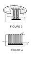
- Fig. 3 shows a diagrammatical, cross-sectional view of a further embodiment according to the invention, in which a first and a second microneedle, each with an access channel 20 are provided.
- the electrode 25 extends on the inner surfaces of both microneedles.
- the effective surface area for stimulating protruding portions of the biological cell 40 is substantially increased.
- the electrode is continuous along the tip of the microneedles and the inner surfaces of both microneedles.
- Fig. 4 shows a diagrammatical, cross-sectional view of another embodiment according to the invention. This embodiment is most suitably manufactured in accordance with the third method as specified above. It comprises a plurality of access channels 20 parallel to each other and defined within the substrate 1.
- the plurality of access channels 20 comprises preferably more than 5 access channels, more preferably at least 10 access channels and even more preferably an array of at least 20 access channels.
- the advantage of this embodiment is a substantial increase in surface area of the electrode 25. Stronger stimulation of the cell may thus be provided. Furthermore, sections of the array of access channels may be isolated to study local differences in behaviour of the cells.
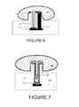
- Fig. 6 shows a diagrammatical, cross-sectional view of a further embodiment according to the invention.
- the microneedle comprises a vertical conductor 5 in addition to the access channel 20.
- the advantage hereof is that a separate sensor and/or actuator may be present on the tip of the microneedle. Particularly, the provision of a sensor is deemed beneficial. It is therewith possible to detect changes in the cell outside the protruding portion 41. When in use as an actuator, it may be beneficial for stimulating the cell to grow into the access channel 20.
- Fig. 7 shows a diagrammatical, cross-sectional view of again another embodiment according to the invention.
- a sensor 24 constitutes the means for sensing and/or actuating.
- the sensor 24 is provided at a sensor port 22, preferably at a bottom of the access channel 20.
- the sensor 24 is manufactured in or directed on top of the semiconductor substrate 1.
- the sensor may be a capacitive sensor, a transistor type sensor, for instance of the type known as a chemFET, a chemical sensor, for instance a pH-sensor.
- the sensor may be tuned for sensing one or more properties occuring during electroporation of the biological cell.
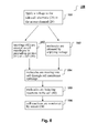
- Fig. 8 shows a sequence 100 of steps occurring in electroporation.
- a first step 101 voltage pulses are applied.
- the voltage of the pulses is preferably in the range of 200 mV-10V.
- the pulses are preferably applied with a duration of nanoseconds, and with a frequency suitably in the range of 1 MHz to appr. 1 GHz.
- step 102 openings are created in the cell membrane of the cell.
- the threshold voltage for formation of such openings depends on the effectiveness of the coupling between the electrode and the cell membrane. The coupling is moreover enhanced by increasing surface area.
- Step 103 occurs preferably simultaneously with the generation of said openings in the cell membrane.
- a reagent is released into the access channel 20 for interaction with the cell.
- the reagent may be released as molecules or ions.
- the reagent may be present, prior to release, at a chemical port in the access channel. It may be provided there during or after manufacture of the device. It may be there in solid form or in a fluid form, e.g. as a solution, suspension, dispersion or (viscous) liquid.
- the reagent When in fluid form, the reagent is suitably transported to the chemical port by means of a microfluidic channel.
- the reagent may be present in functionalized form on the inner surface of the access channel. Self-assembled monolayers may be used for such functionalization.
- the simultaneous occurrence of the release of the reagent (step 103) and the formation of openings (102) may be achieved by choosing a functionalisation that starts release upon application of voltage pulses.
- the release of the reagent may further be initiated differently. For instance, it could be initiated through the provision of culture medium into the access channel.
- the reagent is present in a bottom part of the access channel. When the cell subsequently enters the access channel, the reagent is present.
- Steps 104 and 105 show subsequent steps, in which the reagent first diffuses into the cell through the formed openings in the cell membrane, and thereafter induces a reaction or a physical change in the cell. Again, this is effectively a subsequent phase of the method and the result of the previous step.
- One suitable reagent is for instance a metal ion, such as an alkali metal ion or an earth alkali metal ion, for instance Ca 2+ .
- the amount of metal ion diffused into the cell can subsequently be measured electrically.
- Molecules suitable for functionalization are for instance glutamate enzymes, acetylcholine-enzymes.
- Step 106 shows the sensing of changes resulting induced reaction or induced physical change.
- the sensing is preferably carried out with the sensor within the access channel. However, this is not essential and a sensor at a location differently could be used alternatively.
- Fig. 5A-D show in a series of cross-sectional views the use of the device for electroporation for further explanation. This use is particularly carried out with a device as shown in Fig. 7 .
- Fig. 5A shows the presence of the cell 40 prior to the formation of the protruding portions 41.
- the access channel 20 comprises in this embodiment a sensor 25 at a sensor port and a reagent 30.
- the reagent 30 is in this embodiment present in functionalized and adhered form at an inner surface of the access channel 20.
- Fig. 5B shows the situation after formation of the protruding portion 41 in the access channel 20. This view corresponds to the starting situation of the flow diagram of Fig. 8 . Though the figure shows a sharp angle between the cell and the protruding portion, this is not understood to represent reality appropriately. Additionally, it is believed that the insertion of the cell into the access channel 20 occurs along the inner surface thereof.
- Fig. 5C shows the situation after release of the reagent 30 into the access channel (step 103), caused by the application of an adequate voltage (step 101). Electroporation (step 102) is also indicated in this Figure.
- the reagent 30 is herein shown as droplets within the access channel 20. This may occur with certain reagents having a hydrophilic head and a hydrophobic tail. Such reagents may form small vesicles with the heads at the outside and the tails at the inside. However, it is not deemed necessary that the reagent flows from the inner surface to the protruding portion 41 of the cell in droplet-like structures.
- the reagent 30 may alternatively dissolve in a culture medium within the access channel 20.
- Fig. 5D shows the subsequent situation, after the diffusion of the reagent 30 into the cell 40 (step 104). A reaction may now be induced and resulting changes may be measured, for instance with the sensor 25.
- Synaptogenesis is the formation of distinct synaptic specialisations. It involves a complex series of events, spanning neuronal differentiation and localized induction of presynaptic and postsynaptic differentiation.
- the device as shown in Fig. 7 may be obtained through various manufacturing methods.
- a standard CMOS-metallisation/back-end process is used to fabricate said microneedles.
- This back-end process is carried out on top of a substrate, for example a silicon wafer or a silicon-on-insulator wafer.
- Devices are suitably defined in the substrate according to known methods, including in one embodiment (as shown in Fig 7 ) a sensor 24.
- Metal interconnects as far as needed were embedded in silicon oxide and fabricated using a Cu damascene process.
- An etch stop layer made of for instance SiC, TiN, Si 3 N 4 was deposited on the metal.
- the dielectric layer is non-porous.
- the dielectric material is for instance an organic dielectric or an oxide, such as silicon oxide.
- a suitable deposition technique is PECVD, but alternatives such as a spin-on oxide are not excluded.
- the dielectric layer was patterned to define the access channel 20 aligned with the sensor underneath, particularly using deep-reactive ion etching. In order to expose the sensor at the sensor port, the etch stop layer is locally removed in the access channel. The diameter of the hole ranged in one experiment from 250 nm to 1 ⁇ m, but other diameters could be chosen as well.
- An electrically conductive layer 25 was thereafter deposited in the access channel 20.
- An adhesion layer may be deposited prior to the conductive layer 25.
- the conductive layer may again by covered by a thin dielectric layer, such as an oxide or a nitride.
- Aluminum (AI) and Tungsten (W) are suitable materials for the electrically conductive layer 25, particularly when not covered by an additional dielectric layer. It has a low toxicity.
- a plurality of layers jointly constituting a sensor or an actuator are deposited as conformal coatings in the access channel 20. Materials such as iridium oxide and titanium nitride are suitable for inclusion in a stack operating as a sensor or an actuator.
- the access channel 20 may thereafter filled with a sacrificial layer, which may be a resist also used for patterning in a subsequent step.
- dots of resist are formed on the top of the dielectric layer at locations which are not to be removed.
- the dots covering said locations are slightly larger than the diameter of the access channel 20.
- the extra area of the dots i.e. the area larger than the diameter of the access channel 20, defines the width of the body 15 surrounding the access channel 20.
- the dots may have a diameter of between 100 nm and 6 ⁇ m or between 600 nm and 1200 nm.
- the insulating layer may be etched, for instance by deep reactive ion-etching, leaving a shaft of insulating material of between 50 nm and 1 ⁇ m, for example between 100 and 200 nm surrounding the access channel 20.
- the total width or diameter of the body 15, e.g. the microneedles may be between 100 nm and 6 ⁇ m, for example between 600 and 1200 nm.
- a via may be provided in the dielectric layer prior to definition of the access channel. This via defines an electrical connection to the tip of the microneedle allowing the provision of an additional sensor and/or actuator thereon.
- the additional sensor or actuator is for instance an electrode.
- such via could be present in an adjacent microneedle.
- the electrodes are defined in platina (Pt).
- the manufacture started again with the definition of interconnects, for instance of Cu, as deposited on an insulating layer on a silicon wafer.
- a suitable pattern comprises for instance interconnects with a thickness of 200-500 nm embedded in a dielectric layer, for instance silicon oxide.
- a subsequent dielectric layer for instance with a thickness in the range of 500 nm to 3 ⁇ m is provided thereon.
- Access channels 20 were plasma etched into the dielectric layer.
- a seed layer for instance a Au seed layer was deposited, for instance by sputtering on the dielectric layer and in the access channels, after a cleaning step.
- the semi-manufactured device preferably a set of semi-manufactured devices present on one substrate such as a wafer, were immersed into a solution for a galvanic replacement reaction.
- the solution contained a hexachloroplatinic acid hydrate (H 2 PtCl 6 )-solution with a concentration of 40 mM.
- the reaction time was, in one example, varied between 30 and 180 seconds. Strong magnetic stirring was applied.
- the prepared wafers were rinsed by DI-water and then dried with a nitrogen gun. Subsequently, the dielectric layer, in one example silicon oxide, was etched in a buffered HF solution (BHF, 7:1) for 4-5 minutes to expose the Pt nanoshell tubes, and thereafter rinsed with DI-water.
- BHF buffered HF solution
- the starting template was a semiconductor substrate, for instance of silicon.
- a mask for instance of silicon oxide, was provided on the silicon wafer according to a desired pattern.
- Access channels i.e. trenches
- surfaces of the access channels were made highly conductive by implantation of dopants.
- one or more dielectric layers were deposited.
- a contact was established adjacent to the trench within the area in which dopants were implanted.
- the access channels were covered with a sacrificial layer. Further layers, such as interconnects and suitably a protrusion around the access channel, were provided so as to optimize the device layout. Finally, the sacrificial layer was again removed.
- a body in the form of a microneedle 15 is provided.
- the body comprises an oxide with a height of 6 ⁇ m. Its diameter is in the range of 2.5 ⁇ m to 1.8 ⁇ m.
- An access channel 20 is present inside the microneedle body 15, so that the oxide forms a shaft around the access channel 20.
- the access channel 20 is defined with a diameter from 0.5 to 1.5 ⁇ m. Spacing between individual microneedles ranges from 3 ⁇ m to 1 ⁇ m.
- the body with the access channel was manufactured in accordance with the first embodiment of the manufacturing process as outlined above.
- a layer of TiN is present on top of the microneedle 15.
- Mouse hippocampal neurons are isolated from embryonic day 17 (E17) mice embryos. Before seeding, the surface is coated with poly-L-lysine to improve to adhesion of the cells. The neurons are then seeded on the microneedles..
- Fig. X shows an image resulting from Scanning electron micrographs (SEM).
- SEM Scanning electron micrographs
- the cell 40 is primarily present on top of the array of microneedle bodies 15. At certain spots the neuron visibly engulfs the microneedles 15 very tightly.
- the cell 40 grows inside the access channel, as indicated by arrows in Fig X. This figure demonstrates a tight adhesion of the neuron cell to the microneedle 15. This has been observed for different dimensions of microneedles, for different spacings between individual microneedles and for different diameters of the access channel.
- Z-stacks of cells on microneedles with access channels 20 are made using confocal microscopy. It was observed that actin rings are present in the cell body around the outer part of the microneedles. Actin dots were observed coinciding with the access channels within the microneedles.. This indicates that the cell cytoskeleton grows down into the access channel, and may grow down to the bottom level. It is not the cell as a whole but particularly actin filaments in the cytoskeleton. It is further observed in on the images that the actin dots and the access channel 20 have the same diameter. This leads to the conclusion that the action filaments, e.g. the protruding portion of the cell, is adhered to the inner surface of the access channel 20.
- the invention may be summarized as an electronic device for sensing and/or actuating comprising a device surface to which an biological cell is applied, further comprising a sensor and/or an actuator or other means for sensing and/or actuating, and an access channel with a channel port, said channel port being located in said surface.
- the access channel is designed such that the biological cell entering the access channel is provided access to the sensor.
- the access channel has a longitudinal axis extending in a direction substantially perpendicular to a plane through said channel port. More suitably, the access channel has a restricted volume and an internal surface that is closed except for the channel port.
- the sensor or actuator is present at a sensor port within the access channel.
- the design of the access channel is particularly such that upon adhesion of the cell to the device surface within a cell adhesion area, a protruding portion is formed and enters into the access channel. It is the protruding portion that is thereafter sensed and/or actuated by the means thereto present in the access channel.
- the invention further relates to the use of this device, in one of its various embodiments, particularly for sensing and/or actuating the protruding portion of a cell, particularly a neuron.
- it is used for enabling electroporation of the cell.
- the device may be further used for actuation of a biological cell as part of a cell stimulation treatment.
- the device could be further used for implantation into the human body. It may serve sensing or actuating purposes, but alternatively be used for the provision of a specific medicament to cells.
- the invention thus also relates to a method for the preparation of a medicine, particularly suitable for application to a cell in an electroporation process, wherein an active component is provided to the device of the invention.
- the active component is then stored in the access channel, for instance in a functionalized form attached to at least a portion of the inner surface.
Landscapes
- Health & Medical Sciences (AREA)
- Engineering & Computer Science (AREA)
- Life Sciences & Earth Sciences (AREA)
- Biomedical Technology (AREA)
- Chemical & Material Sciences (AREA)
- Physics & Mathematics (AREA)
- Food Science & Technology (AREA)
- General Physics & Mathematics (AREA)
- Urology & Nephrology (AREA)
- Hematology (AREA)
- Biophysics (AREA)
- Medicinal Chemistry (AREA)
- Analytical Chemistry (AREA)
- Biochemistry (AREA)
- General Health & Medical Sciences (AREA)
- Molecular Biology (AREA)
- Immunology (AREA)
- Pathology (AREA)
- Apparatus Associated With Microorganisms And Enzymes (AREA)
- Investigating Or Analysing Biological Materials (AREA)
- Investigating Or Analyzing Materials By The Use Of Electric Means (AREA)
- Measuring Or Testing Involving Enzymes Or Micro-Organisms (AREA)
- Measurement Of The Respiration, Hearing Ability, Form, And Blood Characteristics Of Living Organisms (AREA)
Abstract
Description
- The invention relates to an electronic device for sensing and/or actuating, comprising a device surface to which a biological cell is applied and means for sensing and/or actuating said biological cell.
- The invention further relates to the use of such an electronic device.
- Sensors comprising micro-electrode arrays are used for measuring electrical activity in small networks of biological cells, such as neurons. Theses sensors are often relatively big and only small matrices or arrays of micro-electrodes can be made. Current state-of-the-art micro-electrode arrays (MEAs) may contain a maximum of 64 electrodes with a minimal spacing of 100 µm between neighbouring electrodes. The electrodes are often made of flat TiN pads with a diameter of maximum 10 µm. For some applications, smaller spacings, e.g. < 10 µm, and a larger nuber of electrodes, e.g. > 60000, may be required.
- On-chip single cell recording of electrical activity using field-effect transistors has been demonstrated for large neurons or tissue slices (see P. Bergveld et al, IEEE Transactions on Biomedical Engineering, 1976. P. Fromherz et al., Science, May 1991, A. Cohen et al, Biosensors and Electronics, January 2004). IN the case of mammalian neurons, e.g. hippocampal neurons, the cells are much smaller, which leads to a less efficient electrical coupling onto the chip surface and make a reliable electrical contact between the cell membrane and the recording device.
- Hoogerwerf et al. have disclosed an array of microneedles for sensing of neurons. The array of microneedles or probes is assembled to a silicon platform with a construction in which the microneedles run through holes in the platform and then are connected using a certain flange. Electrical connection is made with bumps, e.g. eutectic metal bumps or plated contacts on a plated gold beam. The beams are coupled to interconnects extending on the substrate flange and from there extend on the microneedles. Such needles are particularly suitable for probing a cell. The overall array with microneedles bears a large similarity to probe cards with a plurality of probes used for testing integrated circuits. The conductive probes of such an array make contact with selective test pads on the integrated circuits and provide series of suitably digital signals to the integrated circuit for testing proper operation. However, when applying such array of probes to a biological cell, an adequate measuring of cell properties turns out difficult. The cell membrane does not have a solid and fixed plate of test pads. Therefore, an adequate stimulation by electric pulses and subsequent measuring is not achievable.
-
EP-A 1967581 discloses CMOS compatible microneedles. A diagrammatical cross-sectional drawing hereof is shown inFig. 9 . The microneedles 6 are present on asubstrate 1. The compatibility with CMOS is enabled, in one embodiment, with a manufacturing process as typically in use for the manufacture of interconnect structures of integrated circuits. While Hoogerwerf et al provide contacts on the outside of the microneedle,EP1967581 definesconductors 3 and/or microfluidic channels inside the microneedle 6. Thereto a dielectric matrix with aconductor 3 on top of aninterconnect 2 is defined. Subsequently, the dielectric matrix is patterned so as to define the microneedles 6 with an insulating shaft around the conductor. - The use of such CMOS compatible technology for manufacturing results therein that a top surface of the microneedle may be planar. This is particularly the case at a stage during processing of the microneedles, before the partial removal of the dielectric matrix around the microneedles. As a result, a sensor or actuator device 4 may be defined on top of the microneedle 6. The
interconnects 3 and/or microfluidic channels then run towards the sensor or actuator device 4 on top of the microneedle 6. On application of abiological cell 40, engulfment of the microneedle 6 has been found. This engulfment is beneficial as it leads to reduction of the amplitude of a stimulation current for the actuation of the biological cell. - However, it turns out that the area of the sensor or actuator device on top of the microneedle is limited. Increase of the area by increasing the diameter of the microneedle turns out limited, as the engulfment of the microneedle 6 by the
biological cell 40 may be lost, which is undesired. - It is therefore an object of the invention to provide a device of the kind mentioned in the opening paragraph, that allows improved sensing and/or actuator of biological cell It is a further object to use such a device for sensing purposes.
- According to a first aspect of the invention, an electronic device for sensing and/or actuating is provided, comprising a device surface to which a biological cell is to be applied. The device further comprises an access channel with a channel port, said channel port being located in said surface. The access channel has, in one embodiment, a longitudinal axis extending in a direction substantially perpendicular to a plane through said channel port. The access channel further has, in one embodiment, a restricted volume and an internal surface that is substantially closed except for the channel port. Herein the access channel comprises a sensor and/or actuator for sensing or actuating the biological cell, such that the biological cell is provided access to the sensor and/or actuator by entering the access channel.
- It has been found by the inventors of the present invention, that a biological cell, once adhered to a surface with its cell membrane may begin to grow and thus form protruding portions within shapes suitable for such protruding portions.
- This finding has been exploited in the present invention in that the said shape is used as an access channel to the sensor or actuator. In other words, the sensor or actuator is now not located at a top surface of a microneedle, but within an access channel with an internal surface that is closed except for the channel port. Access to the sensor is obtained only after that the biological cell has sufficiently adhered to the device surface so as to begin to form a protruding portion within the access channel. It is also the protruding portion upon which the sensing is carried out. Since the protruding portion is however in direct contact with the rest of the biological cell without any intermediate interruption, such measurements are deemed representative of the complete cell and/or can be transformed into results representative for the complete cell on the basis of some calibration results.
- In one important embodiment, the device surface has a nonplanar shape with an extended surface area. More advantageously, the device surface comprises a portion extending from a substrate, said extended surface area being at least twice of a reference surface area defined by perpendicular projection on the substrate. It has been found in experiments leading to the invention that a proper adhesion is improved by extending the surface area into a nonplanar shape. One suitable nonplanar shape is for instance the provision of a cavity surrounded by one or more wallshaped portions extending from a substrate, within which cavity the channel port of the access channel is defined. The term 'device surface' as used herein specifically refers to the surface within an area in which adhesion or more particularly engulfment occurs.
- Particularly good results have been obtained with microneedles. It has been observed, that biological cells will engulf the microneedles of
EP-A 1967581 . Such engulfing gives rise to a particularly tight coupling between the cell membrane and the surface of the microneedle. The engulfing further improves the electrical coupling between the sensor or actuator and the cell membrane. - In addition to or instead of increasing surface area of the device surface, attraction between the surface and the biological cell may be improved by functionalizing the device surface or portions thereof. Specific functionalizations may be of chemical and/or of electrical nature. An example of a functionalization of a chemical nature is the application of one or more self-assembled monolayers comprising dedicated functional groups. Typical monolayers use thiol as linking groups to a Au surface. Good results may further be obtained with siloxyl-linking groups. Advantageous forms of such monolayer compounds may include protein-resistant chains such as oligoalkylene glycol groups and recognizing or pre-activated groups for binding to the cell membrane. Typically, such preactivated group is a polar group. Suitable silane compounds and their synthesis are for instance known from
EP1607743 A1 (IMEC ref 2003/014) which is included herein by reference. - In one embodiment, the access channel is further provided with a sensor port, at which a sensor is present. Preferably, this sensor port is located at a bottom of the access channel. However, alternatively, the access channel may give access to a cavity, at a surface of which the sensor is present. The advantage of such cavity is that a sensor with a larger surface area may be provided. The sensor is for instance a chemical sensor, such as a pH-sensor. Though experiments typically use isotonic fluids, a chemical reaction may occur at a cell membrane giving rise to deviations of the pH, for instance.
- In another embodiment, the access channel comprises an electrode at a sidewall of the access channel so as to sense and/or actuate the protruding cell portion, for instance by capacitive coupling. The operation of the electrode by means of capacitive coupling could be understood in analogy to the operation of the gate electrode of a field effect transistor: application of a voltage on the electrode will influence a charge distribution within the protruding portion of the biological cell. Variation of the applied voltage may stimulate the protruding portion of the cell to certain behaviour. Such behaviour could turn out to mimic behaviour in cells known to occur, but currently not understood. An example hereof is failures in signal transmission between cells and/or pain observations by patients as a result thereof. Such behaviour could also be stimulated so as to carry out a treatment on a patient. The operation of the electrode is enhanced by enlarging its surface area. It is therefore advantageous that the electrode substantially covers the complete inner surface of the access channel.
- In a particular implementation hereof, the access channel with the electrode on its surface is used as an actuator, for stimulating the cell. A sensor is provided at a location distinct from the access channel. The sensor is used to sense changes occurring as a result of the actuation within the access channel. The location distinct from the access channel may be within another access channel, for instance at a channel port thereof. However, alternative locations are not excluded. One example is a sensor being present in or on a sensing microneedle, that is also engulfed by the cell. Suitably, the sensor is present at a sensor port of an access channel within the sensing microneedle.
- According to another aspect of the invention, a sensor device is provided. The sensor device comprises at least one microneedle on a substrate, which microneedle comprises an access channel with a channel port and a sensor port, which access channel is designed for providing access to a protruding portion of a biological cell to be applied on and/or around the microneedle, which channel port being located at a tip of the microneedle, which access channel is suitably surrounded by a shaft of insulating material. The sensor device further comprises a sensor located at the sensor port.
- According to another aspect of the invention, an electronic device for sensing and/or actuating is provided. The electronic device comprises at least one microneedle on a substrate provided with an access channel with a channel port located at a tip of the microneedle. The access channel is designed for providing access to a protruding portion of a biological cell to be applied on a device surface, e.g. in a cell adhesion area, on and/or around the microneedle. The access channel has a longitudinal axis extending in a direction substantially perpendicular to a plane through said substrate. The access channel has a restricted volume and an internal surface that is substantially closed except for the channel port, and it comprises an electrode at a sidewall for actuating the protruding cell portion.
- According to again another aspect of the invention, a method of sensing and/or actuating a biological cell is provided. The method comprises the steps of:
- providing an electronic device comprising a cell adhesion area at a surface and an access channel with a channel port located at said surface,
- providing a biological cell, such that the cell adheres to the cell adhesion area;
- allowing growing of a protruding portion of the cell into the access channel, and
- sensing and/or actuating the protruding portion of the cell in the access channel.
-
-
Fig. 1 shows a diagrammatical, cross-sectional view of the device of the invention in a first embodiment; -
Fig. 2 shows a diagrammatical, cross-sectional view of the first embodiment after that a biological cell has formed a protruding portion into the access channel; -
Fig. 3 shows a diagrammatical, cross-sectional view of the device of the invention in a second embodiment; -
Fig. 4 shows a diagrammatical, cross-sectional view of the device of the invention in a third embodiment; -
Fig. 5a-d shows in diagrammatical, cross-sectional views a series of steps of the use of the device of the invention for electroporation of a biological cell; -
Fig. 6 shows a diagrammatical, cross-sectional view of the device of the invention in a fourth embodiment; -
Fig. 7 shows a diagrammatical, cross-sectional view of the device of the invention in a fifth embodiment; -
Fig. 8 shows a flow diagram of the use of the device of the invention for electroporation of a biological cell, and -
Fig. 9 shows a diagrammatical, cross-sectional view of a prior art device. - The present invention will be described with respect to particular embodiments and with reference to certain drawings but the invention is not limited thereto but only by the claims. The drawings described are only schematic and are non-limiting. In the drawings, the size of some of the elements may be exaggerated and not drawn on scale for illustrative purposes. The dimensions and the relative dimensions do not correspond to actual reductions to practice of the invention. Same reference numerals in different figures refer to equal or like elements.
-
Fig. 1 shows a diagrammatical, cross-sectional view of the device according to the invention in a first embodiment just after application of a biological cell to the device.Fig. 2 shows the device of the first embodiment in a second state, after which a cell has entered theaccess channel 20. The device comprises a device surface. The device further comprises anaccess channel 20 with achannel port 21. Thechannel port 21 is located within the surface. Theaccess channel 20 has a longitudinal axis A, which in this example, extends substantially perpendicular to a plane through thechannel port 21, or alternatively, a plane through a substrate. Theaccess channel 20 has a restricted volume and an internal surface 29 that is substantially closed except for thechannel port 21. The term 'substantially closed' is understood to mean within the context of the present application, that a further port, such as a chemical port discussed later on, is present within theaccess channel 20. Such further port is however an option. The access channel may thus further be closed except for the channel port. - The
access channel 20 further comprises means 25 for sensing and/or actuating. This is done so that by entering theaccess channel 20, thebiological cell 40 is provided access to thosemeans 25 for sensing and/or actuating. This location for themeans 25 for sensing and/or actuating implies that said sensing and/or actuating is applied to thatportion 41 of thecell 40 that has entered theaccess channel 20. This portion is herein also referred to as a protrudingportion 41 of the cell. It is understood that this protrudingportion 41 is not present when thebiological cell 40 is applied. It is formed by virtue of the template shape offered by theaccess channel 20. - Thus, one may distinguish different phases in the method of the invention. First, a
biological cell 40 is applied. While this application process could be a specific application of individual cells to the device surface, it is suitably a process in which a fluid, e.g. a free culture medium, with a plurality of biological cells is applied. Individual cells thereafter move to the surface. This movement may be caused by diffusion, convection, electromagnetic attraction, for instance by application of a voltage difference, or a combination of such effects. - Suitably, the device surface is designed or treated such that the cell wets the surface. Surface wetting of surfaces is governed by surface tension between the surface material and the liquid present on the surface, and typically expressed by means of the contact angle. The degree of wetting is determined by a force balance between adhesive forces, e.g. attracting liquid molecules to the surface, and cohesive forces, e.g. attracting liquid molecules to each other. Preferably, the surface is hydrophilic. Most suitably, the surface area is increased in that the surface has a non-planar shape, such as a surface of a microneedle or a cavity surface. This will further shift the force balance towards adhesion. This process may be enhanced by geometrical factors. Most suitably such factors enable that an outside, non-adhered portion of the biological cell has an optimized, ideally minimum, surface area. This is for instance achieved by engulfment of a microneedle 15 through the
cell 40. - It is observed that said adhesion process wherein surface wetting occurs may be further improved by application of a suitable surface treatment. One of such surface treatments is the functionalization of the device surface. As a consequence hereof, the mere adhesion may be strengthened by bonding to the surface. This bonding could be a molecular bond, but alternatively hydrogen bonding, as well as Van der Waals bonding reflecting dipole/dipole and/or dipole/induced dipole interactions.
- Subsequently, the
cell 40 as present on, i.e. adhered to, the device surface, may enter theaccess channel 20. This entering turns out not comparable to the process in the previous steps resulting in engulfment. In fact, the inventors believe without desiring to be bound by following hypothesis, that growth occurs such that the protrudingportion 41 of thecell 40 begins to be formed in theaccess channel 20. Such protrudingportion 41 may be formed with all types ofdifferent cells 20. In one scientifically and medically interesting application, thecell 40 is a neuron. The protrudingcell portion 41 may be, in that example, a synapse. - Factors that may contribute to growth of the protruding
portion 41 are for instance an effective diameter of theaccess channel 20, as measured at the channel port; the inside surface of theaccess channel 20 being wettable by thecell membrane 40; a surface that is sufficiently smooth, such that growth or movement of the cell membrane is not hampered by any restrictions; a circular or oval shape as seen in cross-sectional view in a plane substantially parallel to the channel port is preferred. Hence, the access channel is free of corners into which the protruding portion of the cell does not fit. Another contributing measure is the provision of the access channel at the channel port with an increasing diameter. The intention of the latter measure is to prevent a sharp edge between the inner surface of the access channel and the device surface. - One advantage of the provision of the means for sensing and/or actuating inside the access channel is that sensing and/or actuating is (only) applied to that
portion 41 of thecell 40 that has entered theaccess channel 20. This protruding portion is a portion with a limited volume that is nevertheless an integral part of thebiological cell 40. It is moreover such that such protruding portion of thecell 40 has less space or opportunity of diffusion that any portion on a flat surface. This makes that sensing and/or actuating of thecell 40 may be carried out in a more controlled manner and hence is better repeatable. - A further advantage of the provision of the means for sensing and/or actuating inside the access channel is that specific reactions may be carried out and/or may be stimulated to occur which are less feasible - if at all - on a substantially planar surface. One such reaction is electroporation of the cell membrane, another such reaction is synaptogenesis.
- In the embodiment of
Fig. 1 , anelectrode 25 extending along the internal surface of theaccess channel 20 constitutes said means for sensing and/or actuating. Though preferable, it is not necessary that theelectrode 25 covers the complete internal surface of the access channel. Theelectrode 25 may be covered with a dielectric layer, such as an oxide or a nitride. Aninterconnect 3 is present for applying voltages to theelectrode 25. Suitably a diffusion barrier - not shown - is present, for instance of SiC, so as to isolate anunderlying substrate 1 from theaccess channel 20. This diffusion barrier is found to reduce cytotoxicity. In this embodiment, but this is not essential, the device surface has a nonplanar shape with an extended surface area. Particularly, as shown inFig. 1 and 2 , the nonplanar shape is designed so as to enable that thebiological cell 40 engulfs the device surface. In this example, the device surface has a portion extending substantially in parallel to the longitudinal axis A of theaccess channel 20, i.e. at the outside of a block-shaped, a cylinder-shaped or a pillar-shaped body. This body is in a most advantageous embodiment a microneedle, i.e. a structure oriented substantially perpendicular to the plane of the substrate and having a width between 50 nm and 10 µm, for example between 100 nm and 6 µm and a height of between 150 nm and 50 µm. The microneedle may be a shaft of insulating material. Most suitably, theaccess channel 20 is trench shaped, with a oval or circular cross-section parallel to the plane of the channel port. However, it is not excluded that the access channel is provided with an chemical port. Reagents may be present at the chemical port or be transported to said chemical port, for instance by means of a microfluidic channel. It is moreover not excluded that the trench-shaped channel may be provided with a widened portion at its bottom. - In a suitable embodiment, the access channel has an aspect ratio of depth over diameter of more than 1. Preferably, said aspect ratio is 5 or higher, more preferably said aspect ratio is 10 or higher. The access channel suitably has a diameter in the range of 0.1 to 8 microns, preferably 1 to 7.5 microns, more preferably 3 to 7 microns. The access channel suitably has a depth in the range of 0.3 to 15 microns, preferably 1 to 8 microns. In case that the
access channel 20 is present within a microneedle 15 or another body extending from a substrate, the access channel may have a height larger, equal or smaller than said microneedle. Its height may thus be tuned to a specific cell type. In case that the height of the access channel is larger than that of the microneedle 15, this may be achieved by continued etching into an underlying substrate. Alternatively, it may be achieved by covering the substrate outside the microneedle with one or more layers. This effectively reduces the height of the microneedle. Such covering may be achieved by deposition or growth of certain materials, but alternatively by merely partial removal of a template layer while forming the microneedle. - In a further embodiment, functionalization of the access port and/or inner surface - also referred to as sidewall - of the
access channel 20 with proteins or peptides is provided. The said functionalisation attracts thebiological cell 40 or the protrudingportion 41 of thebiological cell 40. Suitable examples of molecules providing functionalization include poly-L-Lysine, laminine, peptides such as RGD and PA22-2. The functionalization may be applied, for instance, with chemisorption and through self-assembled monolayers. - In an even further developed version hereof, the functionalization triggers a specific reaction in the cell. Examples of suitable molecules for this purpose include glutamate receptors, glutamate antibodies, integrines. Examples of reactions that may be triggered include the promotion of focal adhesion as well as certain reception expressions on or in a membrane of the cell.
-
Fig. 3 shows a diagrammatical, cross-sectional view of a further embodiment according to the invention, in which a first and a second microneedle, each with anaccess channel 20 are provided. Theelectrode 25 extends on the inner surfaces of both microneedles. Herewith the effective surface area for stimulating protruding portions of thebiological cell 40 is substantially increased. In this non-limiting embodiment, the electrode is continuous along the tip of the microneedles and the inner surfaces of both microneedles.Fig. 4 shows a diagrammatical, cross-sectional view of another embodiment according to the invention. This embodiment is most suitably manufactured in accordance with the third method as specified above. It comprises a plurality ofaccess channels 20 parallel to each other and defined within thesubstrate 1. The plurality ofaccess channels 20 comprises preferably more than 5 access channels, more preferably at least 10 access channels and even more preferably an array of at least 20 access channels. The advantage of this embodiment is a substantial increase in surface area of theelectrode 25. Stronger stimulation of the cell may thus be provided. Furthermore, sections of the array of access channels may be isolated to study local differences in behaviour of the cells. -
Fig. 6 shows a diagrammatical, cross-sectional view of a further embodiment according to the invention. Herein, the microneedle comprises a vertical conductor 5 in addition to theaccess channel 20. The advantage hereof is that a separate sensor and/or actuator may be present on the tip of the microneedle. Particularly, the provision of a sensor is deemed beneficial. It is therewith possible to detect changes in the cell outside the protrudingportion 41. When in use as an actuator, it may be beneficial for stimulating the cell to grow into theaccess channel 20. -
Fig. 7 shows a diagrammatical, cross-sectional view of again another embodiment according to the invention. Herein asensor 24 constitutes the means for sensing and/or actuating. Thesensor 24 is provided at a sensor port 22, preferably at a bottom of theaccess channel 20. Suitably, thesensor 24 is manufactured in or directed on top of thesemiconductor substrate 1. The sensor may be a capacitive sensor, a transistor type sensor, for instance of the type known as a chemFET, a chemical sensor, for instance a pH-sensor. Particularly the sensor may be tuned for sensing one or more properties occuring during electroporation of the biological cell. -
Fig. 8 shows asequence 100 of steps occurring in electroporation. In afirst step 101, voltage pulses are applied. The voltage of the pulses is preferably in the range of 200 mV-10V. The pulses are preferably applied with a duration of nanoseconds, and with a frequency suitably in the range of 1 MHz to appr. 1 GHz. - The result of the application of voltage pulses is shown as step 102: openings are created in the cell membrane of the cell. The threshold voltage for formation of such openings depends on the effectiveness of the coupling between the electrode and the cell membrane. The coupling is moreover enhanced by increasing surface area.
- Step 103 occurs preferably simultaneously with the generation of said openings in the cell membrane. Herein, a reagent is released into the
access channel 20 for interaction with the cell. The reagent may be released as molecules or ions. The reagent may be present, prior to release, at a chemical port in the access channel. It may be provided there during or after manufacture of the device. It may be there in solid form or in a fluid form, e.g. as a solution, suspension, dispersion or (viscous) liquid. When in fluid form, the reagent is suitably transported to the chemical port by means of a microfluidic channel. Alternatively, the reagent may be present in functionalized form on the inner surface of the access channel. Self-assembled monolayers may be used for such functionalization. The simultaneous occurrence of the release of the reagent (step 103) and the formation of openings (102) may be achieved by choosing a functionalisation that starts release upon application of voltage pulses. However, the release of the reagent may further be initiated differently. For instance, it could be initiated through the provision of culture medium into the access channel. In one specific implementation, the reagent is present in a bottom part of the access channel. When the cell subsequently enters the access channel, the reagent is present. -
Steps - Step 106 shows the sensing of changes resulting induced reaction or induced physical change. The sensing is preferably carried out with the sensor within the access channel. However, this is not essential and a sensor at a location differently could be used alternatively.
-
Fig. 5A-D show in a series of cross-sectional views the use of the device for electroporation for further explanation. This use is particularly carried out with a device as shown inFig. 7 . -
Fig. 5A shows the presence of thecell 40 prior to the formation of the protrudingportions 41. Theaccess channel 20 comprises in this embodiment asensor 25 at a sensor port and areagent 30. Thereagent 30 is in this embodiment present in functionalized and adhered form at an inner surface of theaccess channel 20. -
Fig. 5B shows the situation after formation of the protrudingportion 41 in theaccess channel 20. This view corresponds to the starting situation of the flow diagram ofFig. 8 . Though the figure shows a sharp angle between the cell and the protruding portion, this is not understood to represent reality appropriately. Additionally, it is believed that the insertion of the cell into theaccess channel 20 occurs along the inner surface thereof. -
Fig. 5C shows the situation after release of thereagent 30 into the access channel (step 103), caused by the application of an adequate voltage (step 101). Electroporation (step 102) is also indicated in this Figure. Thereagent 30 is herein shown as droplets within theaccess channel 20. This may occur with certain reagents having a hydrophilic head and a hydrophobic tail. Such reagents may form small vesicles with the heads at the outside and the tails at the inside. However, it is not deemed necessary that the reagent flows from the inner surface to the protrudingportion 41 of the cell in droplet-like structures. Thereagent 30 may alternatively dissolve in a culture medium within theaccess channel 20. -
Fig. 5D shows the subsequent situation, after the diffusion of thereagent 30 into the cell 40 (step 104). A reaction may now be induced and resulting changes may be measured, for instance with thesensor 25. - Synaptogenesis is the formation of distinct synaptic specialisations. It involves a complex series of events, spanning neuronal differentiation and localized induction of presynaptic and postsynaptic differentiation.
- The device as shown in
Fig. 7 may be obtained through various manufacturing methods. According to a first method, a standard CMOS-metallisation/back-end process is used to fabricate said microneedles. This back-end process is carried out on top of a substrate, for example a silicon wafer or a silicon-on-insulator wafer. Devices are suitably defined in the substrate according to known methods, including in one embodiment (as shown inFig 7 ) asensor 24. Metal interconnects as far as needed were embedded in silicon oxide and fabricated using a Cu damascene process. An etch stop layer made of for instance SiC, TiN, Si3N4 was deposited on the metal. - Subsequently, a relatively thick layer of dielectric material is deposited. Preferably, the dielectric layer is non-porous. The dielectric material is for instance an organic dielectric or an oxide, such as silicon oxide. A suitable deposition technique is PECVD, but alternatives such as a spin-on oxide are not excluded. The dielectric layer was patterned to define the
access channel 20 aligned with the sensor underneath, particularly using deep-reactive ion etching. In order to expose the sensor at the sensor port, the etch stop layer is locally removed in the access channel. The diameter of the hole ranged in one experiment from 250 nm to 1 µm, but other diameters could be chosen as well. - An electrically
conductive layer 25 was thereafter deposited in theaccess channel 20. An adhesion layer may be deposited prior to theconductive layer 25. The conductive layer may again by covered by a thin dielectric layer, such as an oxide or a nitride. Aluminum (AI) and Tungsten (W) are suitable materials for the electricallyconductive layer 25, particularly when not covered by an additional dielectric layer. It has a low toxicity. In one embodiment, a plurality of layers jointly constituting a sensor or an actuator are deposited as conformal coatings in theaccess channel 20. Materials such as iridium oxide and titanium nitride are suitable for inclusion in a stack operating as a sensor or an actuator. Theaccess channel 20 may thereafter filled with a sacrificial layer, which may be a resist also used for patterning in a subsequent step. - Subsequently, dots of resist are formed on the top of the dielectric layer at locations which are not to be removed. The dots covering said locations are slightly larger than the diameter of the
access channel 20. The extra area of the dots, i.e. the area larger than the diameter of theaccess channel 20, defines the width of the body 15 surrounding theaccess channel 20. The dots may have a diameter of between 100 nm and 6 µm or between 600 nm and 1200 nm. Thereafter, the insulating layer may be etched, for instance by deep reactive ion-etching, leaving a shaft of insulating material of between 50 nm and 1 µm, for example between 100 and 200 nm surrounding theaccess channel 20. The total width or diameter of the body 15, e.g. the microneedles may be between 100 nm and 6 µm, for example between 600 and 1200 nm. Finally, both the dots of resist and the sacrificial layer are removed. - If desired, a via may be provided in the dielectric layer prior to definition of the access channel. This via defines an electrical connection to the tip of the microneedle allowing the provision of an additional sensor and/or actuator thereon. The additional sensor or actuator is for instance an electrode. Instead of being present within the same microneedle, such via could be present in an adjacent microneedle.
- According to a second implementation of manufacturing the devices according to the invention, the electrodes are defined in platina (Pt). The manufacture started again with the definition of interconnects, for instance of Cu, as deposited on an insulating layer on a silicon wafer. A suitable pattern comprises for instance interconnects with a thickness of 200-500 nm embedded in a dielectric layer, for instance silicon oxide. A subsequent dielectric layer, for instance with a thickness in the range of 500 nm to 3 µm is provided thereon.
Access channels 20 were plasma etched into the dielectric layer. Thereafter, a seed layer, for instance a Au seed layer was deposited, for instance by sputtering on the dielectric layer and in the access channels, after a cleaning step. Unwanted portion of the seed layer, i.e. on the top surface were removed, for instance by mechanical polishing. Thereafter, the semi-manufactured device, preferably a set of semi-manufactured devices present on one substrate such as a wafer, were immersed into a solution for a galvanic replacement reaction. In one example, the solution contained a hexachloroplatinic acid hydrate (H2PtCl6)-solution with a concentration of 40 mM. The reaction time was, in one example, varied between 30 and 180 seconds. Strong magnetic stirring was applied. The prepared wafers were rinsed by DI-water and then dried with a nitrogen gun. Subsequently, the dielectric layer, in one example silicon oxide, was etched in a buffered HF solution (BHF, 7:1) for 4-5 minutes to expose the Pt nanoshell tubes, and thereafter rinsed with DI-water. - According to a third implementation of the method, the starting template was a semiconductor substrate, for instance of silicon. A mask, for instance of silicon oxide, was provided on the silicon wafer according to a desired pattern. Access channels (i.e. trenches) were etched into the silicon using deep reactive ion etching. Subsequently, surfaces of the access channels were made highly conductive by implantation of dopants. Thereafter, one or more dielectric layers, were deposited. A contact was established adjacent to the trench within the area in which dopants were implanted. Suitably, the access channels were covered with a sacrificial layer. Further layers, such as interconnects and suitably a protrusion around the access channel, were provided so as to optimize the device layout. Finally, the sacrificial layer was again removed.
- A body in the form of a microneedle 15 is provided. The body comprises an oxide with a height of 6 µm. Its diameter is in the range of 2.5 µm to 1.8 µm. An
access channel 20 is present inside the microneedle body 15, so that the oxide forms a shaft around theaccess channel 20. Theaccess channel 20 is defined with a diameter from 0.5 to 1.5 µm. Spacing between individual microneedles ranges from 3 µm to 1 µm. The body with the access channel was manufactured in accordance with the first embodiment of the manufacturing process as outlined above. A layer of TiN is present on top of the microneedle 15. - Mouse hippocampal neurons are isolated from embryonic day 17 (E17) mice embryos. Before seeding, the surface is coated with poly-L-lysine to improve to adhesion of the cells. The neurons are then seeded on the microneedles..
- After 1 to 3 days in vitro (DIV), cells are fixed with formaldehyde. Before confocal microscopy imaging can be done, cells must permeabilized with 0.5% Triton X100 and stained for with Phalloidin 488 to visualize the actin filaments present in the cells. Before making scanning electron micrograph pictures, cells are treated with OSO4 and dried by critical point drying.
- Fig. X shows an image resulting from Scanning electron micrographs (SEM). The
cell 40 is primarily present on top of the array of microneedle bodies 15. At certain spots the neuron visibly engulfs the microneedles 15 very tightly. Thecell 40 grows inside the access channel, as indicated by arrows in Fig X. This figure demonstrates a tight adhesion of the neuron cell to the microneedle 15. This has been observed for different dimensions of microneedles, for different spacings between individual microneedles and for different diameters of the access channel. - Z-stacks of cells on microneedles with
access channels 20 are made using confocal microscopy. It was observed that actin rings are present in the cell body around the outer part of the microneedles. Actin dots were observed coinciding with the access channels within the microneedles.. This indicates that the cell cytoskeleton grows down into the access channel, and may grow down to the bottom level. It is not the cell as a whole but particularly actin filaments in the cytoskeleton. It is further observed in on the images that the actin dots and theaccess channel 20 have the same diameter. This leads to the conclusion that the action filaments, e.g. the protruding portion of the cell, is adhered to the inner surface of theaccess channel 20. - The invention may be summarized as an electronic device for sensing and/or actuating comprising a device surface to which an biological cell is applied, further comprising a sensor and/or an actuator or other means for sensing and/or actuating, and an access channel with a channel port, said channel port being located in said surface. The access channel is designed such that the biological cell entering the access channel is provided access to the sensor. Suitably, the access channel has a longitudinal axis extending in a direction substantially perpendicular to a plane through said channel port. More suitably, the access channel has a restricted volume and an internal surface that is closed except for the channel port. In a preferred embodiment, the sensor or actuator is present at a sensor port within the access channel. The design of the access channel is particularly such that upon adhesion of the cell to the device surface within a cell adhesion area, a protruding portion is formed and enters into the access channel. It is the protruding portion that is thereafter sensed and/or actuated by the means thereto present in the access channel.
- The invention further relates to the use of this device, in one of its various embodiments, particularly for sensing and/or actuating the protruding portion of a cell, particularly a neuron. Advantageously, it is used for enabling electroporation of the cell. The device may be further used for actuation of a biological cell as part of a cell stimulation treatment. The device could be further used for implantation into the human body. It may serve sensing or actuating purposes, but alternatively be used for the provision of a specific medicament to cells. The invention thus also relates to a method for the preparation of a medicine, particularly suitable for application to a cell in an electroporation process, wherein an active component is provided to the device of the invention. The active component is then stored in the access channel, for instance in a functionalized form attached to at least a portion of the inner surface.
- It is observed for clarity that the terms first, second, third and the like in the description and in the claims, are used for distinguishing between similar elements and not necessarily for describing a sequence, either temporally, spatially, in ranking or in any other manner. It is to be understood that the terms so used are interchangeable under appropriate circumstances and that the embodiments of the invention described herein are capable of operation in other sequences than described or illustrated herein.
- Moreover, the terms top, bottom, over, under and the like in the description and the claims are used for descriptive purposes and not necessarily for describing relative positions. It is to be understood that the terms so used are interchangeable under appropriate circumstances and that the embodiments of the invention described herein are capable of operation in other orientations than described or illustrated herein.
- It is to be noticed that the term "comprising", used in the claims, should not be interpreted as being restricted to the means listed thereafter; it does not exclude other elements or steps. It is thus to be interpreted as specifying the presence of the stated features, integers, steps or components as referred to, but does not preclude the presence or addition of one or more other features, integers, steps or components, or groups thereof. Thus, the scope of the expression "a device comprising means A and B" should not be limited to devices consisting only of components A and B. It means that with respect to the present invention, the only relevant components of the device are A and B.
Claims (15)
- An electronic device for sensing and/or actuating, comprising:a substrate with a device surface to which a biological cell is applied, andan access channel with a channel port, said channel port being located in said device surface, which access channel has a longitudinal axis extending in a direction substantially perpendicular to a plane through said substrate, which access channel has a restricted volume and an internal surface that is substantially closed except for the channel port, and which access channel further comprises means for sensing and/or actuating the biological cell, such that the biological cell entering the access channel is provided access to the means for sensing and/or actuating.
- The electronic device as claimed in Claim 1, the means for sensing and/or actuating comprise a sensor present at a sensor port in the access channel.
- The electronic device as claimed in Claim 1 or 2, wherein the device surface has a nonplanar shape with an extended surface area.
- The electronic device as claimed in Claim 3, wherein the surface portion extending from the substrate is a microneedle, said channel port being defined at a tip of the microneedle.
- The electronic device as claimed in any of the previous Claims, wherein the access channel comprises an electrode on at least a portion of the inner surface of the access channel so as to sense and/or actuate the cell.
- The electronic device as claimed in Claim 1, wherein the means for sensing and/or actuating comprise an electroporation element with an electrode for applying voltage pulses and with a storage of a reagent suitable for interaction with the cell and/or some parts thereof.
- The electronic device as claimed in Claim 6, wherein the reagent is stored by means of a self-assembled monolayer
- The electronic device as claimed in Claim 1, further comprising a sensor at a location distinct from the access channel
- A sensor device comprising
at least one microneedle on a substrate, which microneedle comprises an access channel with a channel port and a sensor port, which access channel is designed for providing access to biological cell to be applied on and/or around the microneedle, which channel port being located at a tip of the microneedle, and
a sensor located at the sensor port. - An electronic device for sensing and/or actuating, comprising at least one microneedle on a substrate provided with an access channel with a channel port located at a tip of the microneedle, which access channel:is designed for providing access to a biological cell to be applied on a device surface on and/or around the microneedle,has a longitudinal axis extending in a direction substantially perpendicular to a plane through said substrate,has a restricted volume and an internal surface that is substantially closed except for the channel port, andcomprises an electrode at a sidewall for actuating the cell.
- The electronic device as claimed in Claim 10, wherein a sensor is present at a location distinct from the microneedle, which sensor is able to sense a property of the cell upon actuating of the cell through the electrode in the microneedle.
- A method of sensing and/or actuating a biological cell, comprising the steps of:providing an electronic device comprising a device surface and an access channel with a channel port located at said surface, wherein the access channel has a longitudinal axis extending in a direction substantially perpendicular to a plane through said channel port, and has a restricted volume and an internal surface that is substantially closed except for the channel port,providing a biological cell to the device surface;allowing growth of the cell into the access channel, andsensing and/or actuating the cell in the access channel.
- The method as claimed in Claim 12, wherein the biological cell is sensed in a sensor located at a sensor port within the access channel.
- The method as claimed in Claim 12, wherein the biological cell is sensed and/or actuated by means of an electrode at a sidewall of the access channel.
- The method as claimed in Claim 14, wherein the biological cell is actuated by means of the electrode and the biological cell is sensed in a sensor distinct from the access channel.
Priority Applications (5)
| Application Number | Priority Date | Filing Date | Title |
|---|---|---|---|
| EP09180939.2A EP2343550B1 (en) | 2009-12-30 | 2009-12-30 | Improved microneedle |
| PCT/EP2010/070947 WO2011080327A2 (en) | 2009-12-30 | 2010-12-30 | Improved microneedle |
| US13/519,894 US9551698B2 (en) | 2009-12-30 | 2010-12-30 | Microneedle |
| JP2012546453A JP5941411B2 (en) | 2009-12-30 | 2010-12-30 | Electronic device and method for sensing and / or driving biological cells |
| EP10808988.9A EP2519818B1 (en) | 2009-12-30 | 2010-12-30 | Improved microneedle |
Applications Claiming Priority (1)
| Application Number | Priority Date | Filing Date | Title |
|---|---|---|---|
| EP09180939.2A EP2343550B1 (en) | 2009-12-30 | 2009-12-30 | Improved microneedle |
Publications (2)
| Publication Number | Publication Date |
|---|---|
| EP2343550A1 true EP2343550A1 (en) | 2011-07-13 |
| EP2343550B1 EP2343550B1 (en) | 2013-11-06 |
Family
ID=42173650
Family Applications (2)
| Application Number | Title | Priority Date | Filing Date |
|---|---|---|---|
| EP09180939.2A Active EP2343550B1 (en) | 2009-12-30 | 2009-12-30 | Improved microneedle |
| EP10808988.9A Active EP2519818B1 (en) | 2009-12-30 | 2010-12-30 | Improved microneedle |
Family Applications After (1)
| Application Number | Title | Priority Date | Filing Date |
|---|---|---|---|
| EP10808988.9A Active EP2519818B1 (en) | 2009-12-30 | 2010-12-30 | Improved microneedle |
Country Status (4)
| Country | Link |
|---|---|
| US (1) | US9551698B2 (en) |
| EP (2) | EP2343550B1 (en) |
| JP (1) | JP5941411B2 (en) |
| WO (1) | WO2011080327A2 (en) |
Families Citing this family (21)
| Publication number | Priority date | Publication date | Assignee | Title |
|---|---|---|---|---|
| JP2014533523A (en) | 2011-09-02 | 2014-12-15 | ザ レジェンツ オブ ザ ユニヴァーシティー オブ カリフォルニア | Microneedle arrays for biosensing and drug delivery |
| US9933387B1 (en) | 2014-09-07 | 2018-04-03 | Biolinq, Inc. | Miniaturized sub-nanoampere sensitivity low-noise potentiostat system |
| US10092207B1 (en) | 2016-05-15 | 2018-10-09 | Biolinq, Inc. | Tissue-penetrating electrochemical sensor featuring a co-electrodeposited thin film comprised of polymer and bio-recognition element |
| CN118421711A (en) * | 2016-10-31 | 2024-08-02 | 梅科诺有限公司 | Array of needle manipulators for biological cell injection |
| US12109032B1 (en) | 2017-03-11 | 2024-10-08 | Biolinq Incorporated | Methods for achieving an isolated electrical interface between an anterior surface of a microneedle structure and a posterior surface of a support structure |
| US11045142B1 (en) | 2017-04-29 | 2021-06-29 | Biolinq, Inc. | Heterogeneous integration of silicon-fabricated solid microneedle sensors and CMOS circuitry |
| US12599337B1 (en) | 2017-08-08 | 2026-04-14 | Biolinq Incorporated | Method and system for confirmation of microneedle-based analyte-selective sensor insertion into viable tissue via electrical interrogation |
| USD875254S1 (en) | 2018-06-08 | 2020-02-11 | Biolinq, Inc. | Intradermal biosensor |
| US20220031244A1 (en) | 2020-07-29 | 2022-02-03 | Biolinq Inc. | Continuous analyte monitoring system with microneedle array |
| EP4256315A4 (en) | 2020-12-03 | 2024-11-06 | Biolinq Incorporated | REFERENCE ELECTRODE AND COUNTER ELECTRODE INTEGRATED IN A SOLID STATE SUBSTRATE |
| CN117813128A (en) * | 2021-01-22 | 2024-04-02 | 索伦托药业有限公司 | Device for microliter lymphatic delivery of coronavirus vaccine |
| USD988160S1 (en) | 2021-03-16 | 2023-06-06 | Biolinq Incorporated | Wearable dermal sensor |
| EP4153276B1 (en) | 2021-05-08 | 2025-12-10 | Biolinq Incorporated | Fault detection for microneedle array based continuous analyte monitoring device |
| USD1013544S1 (en) | 2022-04-29 | 2024-02-06 | Biolinq Incorporated | Wearable sensor |
| USD996999S1 (en) | 2021-11-16 | 2023-08-29 | Biolinq Incorporated | Wearable sensor |
| USD1012744S1 (en) | 2022-05-16 | 2024-01-30 | Biolinq Incorporated | Wearable sensor with illuminated display |
| EP4658168A2 (en) | 2023-02-02 | 2025-12-10 | Biolinq, Inc. | Method for improved sensor sensitivity of a microneedle-based continuous analyte monitoring system |
| USD1068516S1 (en) | 2023-02-28 | 2025-04-01 | Biolinq Incorporated | Wearable sensor |
| USD1083977S1 (en) | 2023-02-28 | 2025-07-15 | Biolinq Incorporated | Display with graphical user interface for a wearable sensor |
| USD1035004S1 (en) | 2023-02-28 | 2024-07-09 | Biolinq Incorporated | Wearable sensor |
| USD1083640S1 (en) | 2023-05-16 | 2025-07-15 | Biolinq Incorporated | Wearable sensor |
Citations (1)
| Publication number | Priority date | Publication date | Assignee | Title |
|---|---|---|---|---|
| EP1967581A1 (en) * | 2007-03-08 | 2008-09-10 | Interuniversitair Microelektronica Centrum | CMOS compatible microneedle structures |
Family Cites Families (9)
| Publication number | Priority date | Publication date | Assignee | Title |
|---|---|---|---|---|
| US5591139A (en) | 1994-06-06 | 1997-01-07 | The Regents Of The University Of California | IC-processed microneedles |
| DE19841337C1 (en) * | 1998-05-27 | 1999-09-23 | Micronas Intermetall Gmbh | Intracellular manipulation of biological cell contents, assisting injection or removal of substances or cell components |
| EP1276426A4 (en) | 2000-03-09 | 2008-03-19 | Nanopass Ltd | Systems and methods for the transport of fluids through a biological barrier and production techniques for such systems |
| WO2002099408A1 (en) * | 2001-06-05 | 2002-12-12 | Matsushita Electric Industrial Co., Ltd. | Signal detecting sensor provided with multi-electrode |
| CN1863910A (en) * | 2003-10-08 | 2006-11-15 | 国立大学法人京都大学 | Method of introducing nucleic acid |
| US6878538B1 (en) * | 2003-10-28 | 2005-04-12 | Cyto Pulse Sciences, Inc. | Apparatus for receiving and aligning a multiple electrode pair array and a multiple treatment cell for use in electroporation |
| US7285674B2 (en) | 2004-05-06 | 2007-10-23 | Interuniversitair Microelektronica Centrum (Imec) | Silane molecules with pre-activated and protein-resistant functionalities and silane films comprising such molecules |
| US20080206828A1 (en) * | 2005-03-17 | 2008-08-28 | Kyoto University | Device For Introducing Substance Into Cell, Cell Clamping Device and Flow Path Forming Method |
| US20080097352A1 (en) * | 2006-09-12 | 2008-04-24 | Beck Patricia A | Methods of fabricating microneedles with bio-sensory functionality |
-
2009
- 2009-12-30 EP EP09180939.2A patent/EP2343550B1/en active Active
-
2010
- 2010-12-30 US US13/519,894 patent/US9551698B2/en active Active
- 2010-12-30 EP EP10808988.9A patent/EP2519818B1/en active Active
- 2010-12-30 JP JP2012546453A patent/JP5941411B2/en active Active
- 2010-12-30 WO PCT/EP2010/070947 patent/WO2011080327A2/en not_active Ceased
Patent Citations (1)
| Publication number | Priority date | Publication date | Assignee | Title |
|---|---|---|---|---|
| EP1967581A1 (en) * | 2007-03-08 | 2008-09-10 | Interuniversitair Microelektronica Centrum | CMOS compatible microneedle structures |
Non-Patent Citations (5)
| Title |
|---|
| BRAEKEN D ET AL: "Local electrical stimulation of single adherent cells using three-dimensional electrode arrays with small interelectrode distances", ENGINEERING IN MEDICINE AND BIOLOGY SOCIETY, 2009. EMBC 2009. ANNUAL INTERNATIONAL CONFERENCE OF THE IEEE, IEEE, PISCATAWAY, NJ, USA, 3 September 2009 (2009-09-03), pages 2756 - 2759, XP031566609, ISBN: 978-1-4244-3296-7, DOI: 10.1109/IEMBS.2009.5333871 * |
| FUJIMOTO H ET AL: "Electroporation microarray for parallel transfer of small interfering RNA into mammalian cells", ANALYTICAL AND BIOANALYTICAL CHEMISTRY, SPRINGER, HEIDELBERG, DE, vol. 392, no. 7-8, December 2008 (2008-12-01), pages 1309 - 1316, XP002585894, ISSN: 1618-2642, DOI: 10.1007/s00216-008-2423-z * |
| HAN A ET AL: "A single cell multi-analysis system for electrophysiological studies", TRANSDUCERS '03, 12TH INTERNATIONAL CONFERENCE ON SOLID-STATE SENSORS, ACTUATORS AND MICROSYSTEMS, 2003, IEEE, PISCATAWAY, NJ, USA, vol. 1, 9 June 2003 (2003-06-09), pages 674 - 677, XP010646663, ISBN: 0-7803-7731-1 * |
| HUYS ET AL: "Novel concepts for improved communication between nerve cells and silicon electronic devices", SOLID STATE ELECTRONICS, ELSEVIER SCIENCE PUBLISHERS, BARKING, GB, vol. 52, no. 4, 3 December 2007 (2007-12-03), pages 533 - 539, XP022519939, ISSN: 0038-1101, DOI: 10.1016/J.SSE.2007.10.025 * |
| JABER F T ET AL: "Action potential recording from dielectrophoretically positioned neurons inside micro-wells of a planar microelectrode array", JOURNAL OF NEUROSCIENCE METHODS, ELSEVIER SCIENCE PUBLISHER B.V., AMSTERDAM, NL, vol. 182, no. 2, 15 September 2009 (2009-09-15), pages 225 - 235, XP026448193, ISSN: 0165-0270 * |
Also Published As
| Publication number | Publication date |
|---|---|
| JP2013516163A (en) | 2013-05-13 |
| US20130045528A1 (en) | 2013-02-21 |
| US9551698B2 (en) | 2017-01-24 |
| EP2519818B1 (en) | 2014-06-11 |
| WO2011080327A3 (en) | 2011-08-25 |
| WO2011080327A2 (en) | 2011-07-07 |
| JP5941411B2 (en) | 2016-06-29 |
| EP2343550B1 (en) | 2013-11-06 |
| EP2519818A2 (en) | 2012-11-07 |
Similar Documents
| Publication | Publication Date | Title |
|---|---|---|
| EP2343550B1 (en) | Improved microneedle | |
| US8452369B2 (en) | CMOS compatible microneedle structures | |
| JP5555709B2 (en) | Biocompatible electrode | |
| US9014796B2 (en) | Flexible polymer microelectrode with fluid delivery capability and methods for making same | |
| Seymour et al. | Novel multi-sided, microelectrode arrays for implantable neural applications | |
| US10856764B2 (en) | Method for forming a multielectrode conformal penetrating array | |
| US20200261025A1 (en) | System and method for making and implanting high-density electrode arrays | |
| US12157666B2 (en) | Sharp, vertically aligned nanowire electrode arrays, high-yield fabrication and intracellular recording | |
| US11363979B2 (en) | Addressable vertical nanowire probe arrays and fabrication methods | |
| US20190380635A1 (en) | Dual-Sided Biomorphic Polymer-based Microelectrode Array and Fabrication Thereof | |
| CN112717273A (en) | Nerve electrical stimulation electrode with micro-columnar structure and preparation method thereof | |
| WO2009104056A1 (en) | Biochip for electrophysiological measurements | |
| WO2019173572A1 (en) | Low-invasiveness flexible neural mesh implanted through temporarily attachment to low-profile microwire | |
| JP7266035B2 (en) | Nanostructured Platforms and Corresponding Manufacturing Methods for Interfacing with Cells | |
| Held et al. | Microneedle arrays for intracellular recording applications | |
| US20220043028A1 (en) | High-density implantable neural probes | |
| Xiao-Hong et al. | A novel implantable multichannel silicon-based microelectrode | |
| Rechkunov et al. | Neurointerfaces: Review and development | |
| Lee | Development and Translation of a 4096 channel Electrocorticography Recording Grid | |
| WO2023174506A1 (en) | Electrode element for bioelectronics and its manufacturing method | |
| Raj et al. | High-Density Individually Addressable Platinum Nanoelectrodes for Neuroscience Applications | |
| Zhu | Dry-etch benzocyclobutene (BCB) based neural-electronic interface | |
| Wang et al. | Fabrication and properties of 3D flexible parylene-based microelectrode array with silicon tips | |
| Rousseau et al. | Microfabrication of high-density microelectrode arrays for in vitro applications | |
| Jiang | Novel nanowire structures and devices for nanoelectronic bioprobes |
Legal Events
| Date | Code | Title | Description |
|---|---|---|---|
| PUAI | Public reference made under article 153(3) epc to a published international application that has entered the european phase |
Free format text: ORIGINAL CODE: 0009012 |
|
| AK | Designated contracting states |
Kind code of ref document: A1 Designated state(s): AT BE BG CH CY CZ DE DK EE ES FI FR GB GR HR HU IE IS IT LI LT LU LV MC MK MT NL NO PL PT RO SE SI SK SM TR |
|
| AX | Request for extension of the european patent |
Extension state: AL BA RS |
|
| 17P | Request for examination filed |
Effective date: 20120112 |
|
| 17Q | First examination report despatched |
Effective date: 20120425 |
|
| GRAP | Despatch of communication of intention to grant a patent |
Free format text: ORIGINAL CODE: EPIDOSNIGR1 |
|
| INTG | Intention to grant announced |
Effective date: 20130613 |
|
| GRAS | Grant fee paid |
Free format text: ORIGINAL CODE: EPIDOSNIGR3 |
|
| GRAA | (expected) grant |
Free format text: ORIGINAL CODE: 0009210 |
|
| AK | Designated contracting states |
Kind code of ref document: B1 Designated state(s): AT BE BG CH CY CZ DE DK EE ES FI FR GB GR HR HU IE IS IT LI LT LU LV MC MK MT NL NO PL PT RO SE SI SK SM TR |
|
| REG | Reference to a national code |
Ref country code: GB Ref legal event code: FG4D |
|
| REG | Reference to a national code |
Ref country code: CH Ref legal event code: EP |
|
| REG | Reference to a national code |
Ref country code: AT Ref legal event code: REF Ref document number: 639813 Country of ref document: AT Kind code of ref document: T Effective date: 20131215 |
|
| REG | Reference to a national code |
Ref country code: IE Ref legal event code: FG4D |
|
| REG | Reference to a national code |
Ref country code: DE Ref legal event code: R096 Ref document number: 602009019865 Country of ref document: DE Effective date: 20140109 |
|
| REG | Reference to a national code |
Ref country code: NL Ref legal event code: VDEP Effective date: 20131106 |
|
| REG | Reference to a national code |
Ref country code: AT Ref legal event code: MK05 Ref document number: 639813 Country of ref document: AT Kind code of ref document: T Effective date: 20131106 |
|
| REG | Reference to a national code |
Ref country code: LT Ref legal event code: MG4D |
|
| PG25 | Lapsed in a contracting state [announced via postgrant information from national office to epo] |
Ref country code: SE Free format text: LAPSE BECAUSE OF FAILURE TO SUBMIT A TRANSLATION OF THE DESCRIPTION OR TO PAY THE FEE WITHIN THE PRESCRIBED TIME-LIMIT Effective date: 20131106 Ref country code: LT Free format text: LAPSE BECAUSE OF FAILURE TO SUBMIT A TRANSLATION OF THE DESCRIPTION OR TO PAY THE FEE WITHIN THE PRESCRIBED TIME-LIMIT Effective date: 20131106 Ref country code: FI Free format text: LAPSE BECAUSE OF FAILURE TO SUBMIT A TRANSLATION OF THE DESCRIPTION OR TO PAY THE FEE WITHIN THE PRESCRIBED TIME-LIMIT Effective date: 20131106 Ref country code: HR Free format text: LAPSE BECAUSE OF FAILURE TO SUBMIT A TRANSLATION OF THE DESCRIPTION OR TO PAY THE FEE WITHIN THE PRESCRIBED TIME-LIMIT Effective date: 20131106 Ref country code: NO Free format text: LAPSE BECAUSE OF FAILURE TO SUBMIT A TRANSLATION OF THE DESCRIPTION OR TO PAY THE FEE WITHIN THE PRESCRIBED TIME-LIMIT Effective date: 20140206 Ref country code: IS Free format text: LAPSE BECAUSE OF FAILURE TO SUBMIT A TRANSLATION OF THE DESCRIPTION OR TO PAY THE FEE WITHIN THE PRESCRIBED TIME-LIMIT Effective date: 20140306 Ref country code: NL Free format text: LAPSE BECAUSE OF FAILURE TO SUBMIT A TRANSLATION OF THE DESCRIPTION OR TO PAY THE FEE WITHIN THE PRESCRIBED TIME-LIMIT Effective date: 20131106 |
|
| PG25 | Lapsed in a contracting state [announced via postgrant information from national office to epo] |
Ref country code: BE Free format text: LAPSE BECAUSE OF FAILURE TO SUBMIT A TRANSLATION OF THE DESCRIPTION OR TO PAY THE FEE WITHIN THE PRESCRIBED TIME-LIMIT Effective date: 20131106 Ref country code: AT Free format text: LAPSE BECAUSE OF FAILURE TO SUBMIT A TRANSLATION OF THE DESCRIPTION OR TO PAY THE FEE WITHIN THE PRESCRIBED TIME-LIMIT Effective date: 20131106 Ref country code: LV Free format text: LAPSE BECAUSE OF FAILURE TO SUBMIT A TRANSLATION OF THE DESCRIPTION OR TO PAY THE FEE WITHIN THE PRESCRIBED TIME-LIMIT Effective date: 20131106 Ref country code: ES Free format text: LAPSE BECAUSE OF FAILURE TO SUBMIT A TRANSLATION OF THE DESCRIPTION OR TO PAY THE FEE WITHIN THE PRESCRIBED TIME-LIMIT Effective date: 20131106 |
|
| PG25 | Lapsed in a contracting state [announced via postgrant information from national office to epo] |
Ref country code: PT Free format text: LAPSE BECAUSE OF FAILURE TO SUBMIT A TRANSLATION OF THE DESCRIPTION OR TO PAY THE FEE WITHIN THE PRESCRIBED TIME-LIMIT Effective date: 20140306 |
|
| PG25 | Lapsed in a contracting state [announced via postgrant information from national office to epo] |
Ref country code: EE Free format text: LAPSE BECAUSE OF FAILURE TO SUBMIT A TRANSLATION OF THE DESCRIPTION OR TO PAY THE FEE WITHIN THE PRESCRIBED TIME-LIMIT Effective date: 20131106 |
|
| REG | Reference to a national code |
Ref country code: CH Ref legal event code: PL |
|
| REG | Reference to a national code |
Ref country code: DE Ref legal event code: R097 Ref document number: 602009019865 Country of ref document: DE |
|
| PG25 | Lapsed in a contracting state [announced via postgrant information from national office to epo] |
Ref country code: SK Free format text: LAPSE BECAUSE OF FAILURE TO SUBMIT A TRANSLATION OF THE DESCRIPTION OR TO PAY THE FEE WITHIN THE PRESCRIBED TIME-LIMIT Effective date: 20131106 Ref country code: PL Free format text: LAPSE BECAUSE OF FAILURE TO SUBMIT A TRANSLATION OF THE DESCRIPTION OR TO PAY THE FEE WITHIN THE PRESCRIBED TIME-LIMIT Effective date: 20131106 Ref country code: IT Free format text: LAPSE BECAUSE OF FAILURE TO SUBMIT A TRANSLATION OF THE DESCRIPTION OR TO PAY THE FEE WITHIN THE PRESCRIBED TIME-LIMIT Effective date: 20131106 Ref country code: RO Free format text: LAPSE BECAUSE OF FAILURE TO SUBMIT A TRANSLATION OF THE DESCRIPTION OR TO PAY THE FEE WITHIN THE PRESCRIBED TIME-LIMIT Effective date: 20131106 Ref country code: CZ Free format text: LAPSE BECAUSE OF FAILURE TO SUBMIT A TRANSLATION OF THE DESCRIPTION OR TO PAY THE FEE WITHIN THE PRESCRIBED TIME-LIMIT Effective date: 20131106 |
|
| PLBE | No opposition filed within time limit |
Free format text: ORIGINAL CODE: 0009261 |
|
| STAA | Information on the status of an ep patent application or granted ep patent |
Free format text: STATUS: NO OPPOSITION FILED WITHIN TIME LIMIT |
|
| REG | Reference to a national code |
Ref country code: IE Ref legal event code: MM4A |
|
| PG25 | Lapsed in a contracting state [announced via postgrant information from national office to epo] |
Ref country code: DK Free format text: LAPSE BECAUSE OF FAILURE TO SUBMIT A TRANSLATION OF THE DESCRIPTION OR TO PAY THE FEE WITHIN THE PRESCRIBED TIME-LIMIT Effective date: 20131106 |
|
| 26N | No opposition filed |
Effective date: 20140807 |
|
| PG25 | Lapsed in a contracting state [announced via postgrant information from national office to epo] |
Ref country code: CH Free format text: LAPSE BECAUSE OF NON-PAYMENT OF DUE FEES Effective date: 20131231 Ref country code: IE Free format text: LAPSE BECAUSE OF NON-PAYMENT OF DUE FEES Effective date: 20131230 Ref country code: LI Free format text: LAPSE BECAUSE OF NON-PAYMENT OF DUE FEES Effective date: 20131231 |
|
| REG | Reference to a national code |
Ref country code: DE Ref legal event code: R097 Ref document number: 602009019865 Country of ref document: DE Effective date: 20140807 |
|
| PG25 | Lapsed in a contracting state [announced via postgrant information from national office to epo] |
Ref country code: SI Free format text: LAPSE BECAUSE OF FAILURE TO SUBMIT A TRANSLATION OF THE DESCRIPTION OR TO PAY THE FEE WITHIN THE PRESCRIBED TIME-LIMIT Effective date: 20131106 |
|
| PG25 | Lapsed in a contracting state [announced via postgrant information from national office to epo] |
Ref country code: MC Free format text: LAPSE BECAUSE OF FAILURE TO SUBMIT A TRANSLATION OF THE DESCRIPTION OR TO PAY THE FEE WITHIN THE PRESCRIBED TIME-LIMIT Effective date: 20131106 |
|
| PG25 | Lapsed in a contracting state [announced via postgrant information from national office to epo] |
Ref country code: SM Free format text: LAPSE BECAUSE OF FAILURE TO SUBMIT A TRANSLATION OF THE DESCRIPTION OR TO PAY THE FEE WITHIN THE PRESCRIBED TIME-LIMIT Effective date: 20131106 |
|
| PG25 | Lapsed in a contracting state [announced via postgrant information from national office to epo] |
Ref country code: CY Free format text: LAPSE BECAUSE OF FAILURE TO SUBMIT A TRANSLATION OF THE DESCRIPTION OR TO PAY THE FEE WITHIN THE PRESCRIBED TIME-LIMIT Effective date: 20131106 Ref country code: TR Free format text: LAPSE BECAUSE OF FAILURE TO SUBMIT A TRANSLATION OF THE DESCRIPTION OR TO PAY THE FEE WITHIN THE PRESCRIBED TIME-LIMIT Effective date: 20131106 |
|
| PG25 | Lapsed in a contracting state [announced via postgrant information from national office to epo] |
Ref country code: BG Free format text: LAPSE BECAUSE OF FAILURE TO SUBMIT A TRANSLATION OF THE DESCRIPTION OR TO PAY THE FEE WITHIN THE PRESCRIBED TIME-LIMIT Effective date: 20131106 Ref country code: LU Free format text: LAPSE BECAUSE OF NON-PAYMENT OF DUE FEES Effective date: 20131230 Ref country code: MK Free format text: LAPSE BECAUSE OF FAILURE TO SUBMIT A TRANSLATION OF THE DESCRIPTION OR TO PAY THE FEE WITHIN THE PRESCRIBED TIME-LIMIT Effective date: 20131106 Ref country code: HU Free format text: LAPSE BECAUSE OF FAILURE TO SUBMIT A TRANSLATION OF THE DESCRIPTION OR TO PAY THE FEE WITHIN THE PRESCRIBED TIME-LIMIT; INVALID AB INITIO Effective date: 20091230 |
|
| PG25 | Lapsed in a contracting state [announced via postgrant information from national office to epo] |
Ref country code: GR Free format text: LAPSE BECAUSE OF NON-PAYMENT OF DUE FEES Effective date: 20131106 Ref country code: MT Free format text: LAPSE BECAUSE OF FAILURE TO SUBMIT A TRANSLATION OF THE DESCRIPTION OR TO PAY THE FEE WITHIN THE PRESCRIBED TIME-LIMIT Effective date: 20131106 |
|
| REG | Reference to a national code |
Ref country code: FR Ref legal event code: PLFP Year of fee payment: 7 |
|
| PG25 | Lapsed in a contracting state [announced via postgrant information from national office to epo] |
Ref country code: GR Free format text: LAPSE BECAUSE OF FAILURE TO SUBMIT A TRANSLATION OF THE DESCRIPTION OR TO PAY THE FEE WITHIN THE PRESCRIBED TIME-LIMIT Effective date: 20140207 |
|
| REG | Reference to a national code |
Ref country code: FR Ref legal event code: PLFP Year of fee payment: 8 |
|
| REG | Reference to a national code |
Ref country code: FR Ref legal event code: PLFP Year of fee payment: 9 |
|
| P01 | Opt-out of the competence of the unified patent court (upc) registered |
Effective date: 20230513 |
|
| PGFP | Annual fee paid to national office [announced via postgrant information from national office to epo] |
Ref country code: DE Payment date: 20251126 Year of fee payment: 17 |
|
| PGFP | Annual fee paid to national office [announced via postgrant information from national office to epo] |
Ref country code: GB Payment date: 20251119 Year of fee payment: 17 |
|
| PGFP | Annual fee paid to national office [announced via postgrant information from national office to epo] |
Ref country code: FR Payment date: 20251120 Year of fee payment: 17 |