EP2343403B1 - Electrochemical method for manufacturing one or more of silicon nanowire and silicon nanotube - Google Patents
Electrochemical method for manufacturing one or more of silicon nanowire and silicon nanotube Download PDFInfo
- Publication number
- EP2343403B1 EP2343403B1 EP09824414.8A EP09824414A EP2343403B1 EP 2343403 B1 EP2343403 B1 EP 2343403B1 EP 09824414 A EP09824414 A EP 09824414A EP 2343403 B1 EP2343403 B1 EP 2343403B1
- Authority
- EP
- European Patent Office
- Prior art keywords
- silicon
- sio
- powder
- nanowires
- nanotubes
- Prior art date
- Legal status (The legal status is an assumption and is not a legal conclusion. Google has not performed a legal analysis and makes no representation as to the accuracy of the status listed.)
- Active
Links
Images



Classifications
-
- C—CHEMISTRY; METALLURGY
- C01—INORGANIC CHEMISTRY
- C01B—NON-METALLIC ELEMENTS; COMPOUNDS THEREOF; METALLOIDS OR COMPOUNDS THEREOF NOT COVERED BY SUBCLASS C01C
- C01B33/00—Silicon; Compounds thereof
- C01B33/02—Silicon
- C01B33/021—Preparation
-
- C—CHEMISTRY; METALLURGY
- C25—ELECTROLYTIC OR ELECTROPHORETIC PROCESSES; APPARATUS THEREFOR
- C25B—ELECTROLYTIC OR ELECTROPHORETIC PROCESSES FOR THE PRODUCTION OF COMPOUNDS OR NON-METALS; APPARATUS THEREFOR
- C25B1/00—Electrolytic production of inorganic compounds or non-metals
- C25B1/01—Products
- C25B1/33—Silicon
-
- C—CHEMISTRY; METALLURGY
- C30—CRYSTAL GROWTH
- C30B—SINGLE-CRYSTAL GROWTH; UNIDIRECTIONAL SOLIDIFICATION OF EUTECTIC MATERIAL OR UNIDIRECTIONAL DEMIXING OF EUTECTOID MATERIAL; REFINING BY ZONE-MELTING OF MATERIAL; PRODUCTION OF A HOMOGENEOUS POLYCRYSTALLINE MATERIAL WITH DEFINED STRUCTURE; SINGLE CRYSTALS OR HOMOGENEOUS POLYCRYSTALLINE MATERIAL WITH DEFINED STRUCTURE; AFTER-TREATMENT OF SINGLE CRYSTALS OR A HOMOGENEOUS POLYCRYSTALLINE MATERIAL WITH DEFINED STRUCTURE; APPARATUS THEREFOR
- C30B29/00—Single crystals or homogeneous polycrystalline material with defined structure characterised by the material or by their shape
- C30B29/02—Elements
- C30B29/06—Silicon
-
- C—CHEMISTRY; METALLURGY
- C30—CRYSTAL GROWTH
- C30B—SINGLE-CRYSTAL GROWTH; UNIDIRECTIONAL SOLIDIFICATION OF EUTECTIC MATERIAL OR UNIDIRECTIONAL DEMIXING OF EUTECTOID MATERIAL; REFINING BY ZONE-MELTING OF MATERIAL; PRODUCTION OF A HOMOGENEOUS POLYCRYSTALLINE MATERIAL WITH DEFINED STRUCTURE; SINGLE CRYSTALS OR HOMOGENEOUS POLYCRYSTALLINE MATERIAL WITH DEFINED STRUCTURE; AFTER-TREATMENT OF SINGLE CRYSTALS OR A HOMOGENEOUS POLYCRYSTALLINE MATERIAL WITH DEFINED STRUCTURE; APPARATUS THEREFOR
- C30B29/00—Single crystals or homogeneous polycrystalline material with defined structure characterised by the material or by their shape
- C30B29/60—Single crystals or homogeneous polycrystalline material with defined structure characterised by the material or by their shape characterised by shape
-
- C—CHEMISTRY; METALLURGY
- C30—CRYSTAL GROWTH
- C30B—SINGLE-CRYSTAL GROWTH; UNIDIRECTIONAL SOLIDIFICATION OF EUTECTIC MATERIAL OR UNIDIRECTIONAL DEMIXING OF EUTECTOID MATERIAL; REFINING BY ZONE-MELTING OF MATERIAL; PRODUCTION OF A HOMOGENEOUS POLYCRYSTALLINE MATERIAL WITH DEFINED STRUCTURE; SINGLE CRYSTALS OR HOMOGENEOUS POLYCRYSTALLINE MATERIAL WITH DEFINED STRUCTURE; AFTER-TREATMENT OF SINGLE CRYSTALS OR A HOMOGENEOUS POLYCRYSTALLINE MATERIAL WITH DEFINED STRUCTURE; APPARATUS THEREFOR
- C30B9/00—Single-crystal growth from melt solutions using molten solvents
- C30B9/14—Single-crystal growth from melt solutions using molten solvents by electrolysis
-
- Y—GENERAL TAGGING OF NEW TECHNOLOGICAL DEVELOPMENTS; GENERAL TAGGING OF CROSS-SECTIONAL TECHNOLOGIES SPANNING OVER SEVERAL SECTIONS OF THE IPC; TECHNICAL SUBJECTS COVERED BY FORMER USPC CROSS-REFERENCE ART COLLECTIONS [XRACs] AND DIGESTS
- Y10—TECHNICAL SUBJECTS COVERED BY FORMER USPC
- Y10S—TECHNICAL SUBJECTS COVERED BY FORMER USPC CROSS-REFERENCE ART COLLECTIONS [XRACs] AND DIGESTS
- Y10S977/00—Nanotechnology
- Y10S977/70—Nanostructure
- Y10S977/762—Nanowire or quantum wire, i.e. axially elongated structure having two dimensions of 100 nm or less
-
- Y—GENERAL TAGGING OF NEW TECHNOLOGICAL DEVELOPMENTS; GENERAL TAGGING OF CROSS-SECTIONAL TECHNOLOGIES SPANNING OVER SEVERAL SECTIONS OF THE IPC; TECHNICAL SUBJECTS COVERED BY FORMER USPC CROSS-REFERENCE ART COLLECTIONS [XRACs] AND DIGESTS
- Y10—TECHNICAL SUBJECTS COVERED BY FORMER USPC
- Y10S—TECHNICAL SUBJECTS COVERED BY FORMER USPC CROSS-REFERENCE ART COLLECTIONS [XRACs] AND DIGESTS
- Y10S977/00—Nanotechnology
- Y10S977/70—Nanostructure
- Y10S977/813—Of specified inorganic semiconductor composition, e.g. periodic table group IV-VI compositions
- Y10S977/814—Group IV based elements and compounds, e.g. CxSiyGez, porous silicon
-
- Y—GENERAL TAGGING OF NEW TECHNOLOGICAL DEVELOPMENTS; GENERAL TAGGING OF CROSS-SECTIONAL TECHNOLOGIES SPANNING OVER SEVERAL SECTIONS OF THE IPC; TECHNICAL SUBJECTS COVERED BY FORMER USPC CROSS-REFERENCE ART COLLECTIONS [XRACs] AND DIGESTS
- Y10—TECHNICAL SUBJECTS COVERED BY FORMER USPC
- Y10S—TECHNICAL SUBJECTS COVERED BY FORMER USPC CROSS-REFERENCE ART COLLECTIONS [XRACs] AND DIGESTS
- Y10S977/00—Nanotechnology
- Y10S977/84—Manufacture, treatment, or detection of nanostructure
- Y10S977/895—Manufacture, treatment, or detection of nanostructure having step or means utilizing chemical property
- Y10S977/896—Chemical synthesis, e.g. chemical bonding or breaking
- Y10S977/899—Electrolytic
Definitions
- the present invention relates to an electrochemical method for fabricating silicon nanowires and silicon nanotubes.
- PECVD plasma enhanced chemical vapour deposition
- Zeng X B, Xu Y Y, Zhang S B, et al. Journal of Crystal Growth, 2003, 247 (1):13 ⁇ 16 a plasma enhanced chemical vapour deposition
- a thermal vapour deposition Feng S Q, Yu D P, Zhang H Z, et al. Journal of Crystal Growth, 2000, 209:513 ⁇ 517
- a solution technique Holmes J D, Johnston K P, Doty R C, et al. Science, 2000, 287:1471 ⁇ 1473
- a selective plating KokKeong L, Joan M R.
- Nanowires produced by laser ablation method has high yield and high purity. But its shortcoming is high costs for expensive equipments.
- chemical vapor deposition (CVD) and thermal chemical vapor deposition techniques are relatively low costs, but the products' diameters vary over a wide range. The products also contain plentiful nano-chains.
- Solution-grown technique can produce nanowires with high length-diameter ratio, but requires using noble metals as catalyst. In addition, the organic and toxic solution has to be recycled, since it will pollute the environment. Other techniques, such as selective plating etc., the yields of nanowires are quite low. The shortcomings of all the above-mentioned techniques hamper the industrial use of nanowires.
- This invention provides an electrochemical method as in claim 1 for producing one or more of silicon nanowires and nanotubes directly from silicon compound SiO 2 powder or a powdered mixture containing silicon compound SiO 2 and other species.
- the method has many advantages: 1) shorter production processing, 2) inexpensive equipment, 3) convenient operation, 4) reduction of contaminants, 5) easily available feed materials, and 6) easy to achieve continuous production.
- the present invention describes the electrochemical method for making Si nanowires or Si nanotubes directly from silicon compound SiO 2 powder.
- the electrochemical method uses an electrolysis cell which may comprises a silicon compound SiO 2 cathode, an anode, and a molten salt electrolyte which may contain metal compound. Electrolysis occurs when a potential is applied between the cathode and the anode. Products including Si nanowires and/or Si nanotubes can be obtained on the cathode.
- the electrochemical method for producing nanowires and/or nanotubes containing silicon directly from a powder mixture containing silicon compound SiO 2 may comprise a silicon compound SiO 2 cathode, an anode and a molten salt electrolyte containing metal compound. Electrolysis occurs when a potential is applied between the anode and the cathode.
- the obtained electrolysis products on the cathode include at least one of Si nanowires and Si nanotubes.
- the electrolysis products on the cathode include 1) silicon nanowires and silicon nanotubes or 2) only silicon nanowires.
- the average diameter of the silicon compound SiO 2 powder may be less than 1 ⁇ m.
- the mixture containing silicon compound SiO 2 may be a mixture prepared by adding metal, alloy, metal compound M 1 Y and/or nonmetal into silicon compound SiO 2 powder, wherein the metal, alloy, metal compound M 1 Y and nonmetal are powder forms.
- the metal may be Au, Pt, Ag, Cu, Fe, Co, Ni, Cr, Mo, Zr, Ti, Al, Mg and/or Nb.
- the mentioned alloy may comprise at least two metals selected from the group of Au, Pt, Ag, Cu, Fe, Co, Ni, Cr, Mo, Zr. Ti, Al, Mg and Nb.
- the M 1 may be Au, Pt, Ag, Cu, Fe, Co, Ni, Cr, Mo, Zr, Ti, Al, Mg or Nb; Y may be O, S, C or N.
- the non-metal may be C, Si, Ge, S, P and/or B.
- the metal compound of the metal compound of the molten salt may be represented by formula MY 1 , wherein M is Ca, Ba, Li, Al, Cs, Na, K or Sr; and Y 1 is Cl or F.
- the molten salt electrolyte containing metal compound may contain one or more electrolyte salts.
- the electrolyte may comprise CaO, which is produced by hydrolyzing fused CaCl 2 at high temperature.
- the potential applied between the cathode and the anode is less than 3.2V.
- the potential applied between the cathode and the anode is less than the decomposition potential of electrolyte.
- the temperature range for the electrolysis is preferably between 500 °C and 1000°C.
- the diameter of the silicon nanowires is less than 100nm.
- the diameter of the silicon nanotubes is less than 100nm.
- the electrolysis products comprise Si nanowires having a diameter less than 100nm and/or Si nanotubes having a diameter less than 100nm.
- the electrolytic products comprise one or more species selected from the group of Si nanowires and nanotubes.
- the electrochemical method for producing silicon nanowires and/or silicon nanotubes directly from silicon compound SiO 2 or a mixture containing silicon compound SiO 2 comprises:
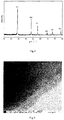
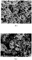
- Fig 1 and Fig 2 are scanning electron microscopy and transmission electron microscopy of a typical electrolysis products prepared from pure nanometer silicon dioxide respectively. Both figures show that the silicon nanowires' and nanotubes' diameters are between 50 - 100 nm and lengths are 2-5 ⁇ m. Shown in Fig 3 is the X-ray diffraction pattern of a silicon crystal product. Shown in Fig 4 is high-resolution transmission electron microscopy image of electrolytic product, it indicates that the surface of the silicon nanowires has amorphous silicon dioxide layer. The d spacing of silicon crystal is about 0.31nm (by measure and calculation), this indicates that the silicon plane is (111). Silicon nanowires and nanotubes produced from pure silicon dioxide at different temperatures are shown in Fig 5 , and silicon nanograin (outside of the invention) produced from the same at different temperatures are shown in Fig 6 .
- nano-SiO 2 powder in the starting material of the following examples is a powder having diameters less than 100nm.
- Examples 1-3 relate to produce pure silicon nanowires and nanotubes by electrolytic reduction of SiO 2 .
- a SiO 2 powder having a purity of 99.95wt% and an average diameter of 0.2 ⁇ m is mixed with a binder.
- the amount of the SiO 2 powder in the total mixture is 75wt% and that of the binder is 25wt%.
- the mixture is pressed into a porous pellet with 10 mm in diameter, 1.1mm in thickness by 5MPa mechanical stress, and then it is sintered at 1100°C in air for about 5 hours. After that, the sintered SiO 2 pellets are combined with a current collector to form a cathode.
- a graphite rod is used as an anode and molten CaCl 2 is used as an electrolyte. Electrolysis is carried out at 800°C, 3.0V in argon atmosphere.
- Fig 1 The final products shown in Fig 1 are curved silicon nanowires having a diameter of about 50nm and a length of 2-5 ⁇ m.
- a SiO 2 powder having a purity of 99.95wt% and an average diameter of 0.25 ⁇ m is mixed with a binder.
- the amount of the SiO 2 powder in the total mixture is 75wt% and that of the binder is 25wt%.
- the mixture is pressed into a porous pellet with 10 mm in diameter, 1.2mm in thickness by 10MPa mechanical stress, and then it is sintered at 1200°C in air for about 4 hours. After that, the sintered SiO 2 pellets are combined with a current collector to form a cathode.
- a graphite rod is used as an anode and molten CaCl 2 is used as an electrolyte. Electrolysis is carried out at 1000°C, 2.0V in helium atmosphere.
- Fig 5 After electrolysis for 4 hours, the electrolytic products are washed by 1 vol% dilute hydrochloric acid, distilled water and anhydrous ethanol. Then the product is dried in a vacuum.
- the final products shown in Fig 5 are curved silicon nanowires and nanotubes having a diameters of between 50-100nm and a lengths of 2-5 ⁇ m, Fig. 5 also show some small amount of micrometre spheres.
- a SiO 2 powder having a purity of 99.95wt% is mixed with a binder.
- the amount of the SiO 2 powder in the total mixture is 75wt% and that of the binder is 25wt%.
- the mixture is pressed into a porous pellet with 10 mm in diameter, 1.5mm in thickness by 15MPa mechanical stress, and then it is sintered at 100°C in air for about 1.5 hours, and then at 1100°C in air for 3 hours. After that, the sintered SiO 2 pellets are combined with a current collector to form a cathode.
- a graphite rod is used as an anode and molten CaCl 2 +NaCl are used as an electrolyte, wherein the ratio of CaCl 2 and NaCl is 51/49 in weight.
- Electrolysis is carried out at 600°C, 2.5V in helium atmosphere. After electrolysis for 5 hours, the electrolytic products are washed by 1 vol% dilute hydrochloric acid, distilled water and anhydrous ethanol in turns. Then the product is dried in a vacuum.
- the final products shown in Fig 6 are mostly silicon nano spheres (outside of the present invention) having a diameter of 30-50nm. A small amount of silicon nanowires and nanotubes can be seen under high-resolution electron microscopy.
- Fig 7 to Fig 12 show silicon nanograin (outside of the invention), and nanowires and/or nanotubes (of the present invention) produced with silicon compound SiO 2 mixture as starting material.
- Examples 4-10 relate to producing silicon nanopowder (outside of the invention), and nanowires and/or nanotubes (of the present invention) by electrolytic reduction method from silicon dioxide comprising conductive material.
- a SiO 2 powder having a purity of 99.95wt% is mixed with an A.R. Ag powder having a grain size of 300M.
- the amount of the SiO 2 powder in the total mixture is 75wt% and that of Ag powder is 25wt%.
- distilled water that 50wt% of the total mixture is added.
- the mixture is pressed into a porous pellet with 10 mm in diameter, 1.5mm in thickness by 15MPa mechanical stress, and then is sintered at 100°C in air for about 1.5 hours, and then at 800°C in air for 3 hours. After that, the sintered SiO 2 pellets are combined with a current collector to form a cathode.
- a graphite rod is used as an anode and molten CaCl 2 +NaCl is used as an electrolyte, wherein the ratio of CaCl 2 and NaCl is 51/49 in weight.
- Electrolysis is carried out at 800°C, 2.5V in argon atmosphere. After electrolysis for 5 hours, the electrolytic products are washed by 1 vol% dilute hydrochloric acid, distilled water and anhydrous ethanol. Then the product is dried in a vacuum.
- the final products shown in Fig 7 are silicon nanowires and nanotubes having diameters of about 30nm and lengths of about 1 ⁇ m. The nanowires and nanotubes are curved and have smooth surface.
- a SiO 2 powder having a purity of 99.95wt% is mixed with an A.R. Co powder having a grain size of 200nm.
- the amount of the SiO 2 powder in the total mixture is 80wt% and that of Co powder is 20wt%.
- distilled water that 50wt% of the total mixture is added.
- the mixture is pressed into a porous pellet with 10 mm in diameter, 1.5mm in thickness by 4MPa mechanical stress, and then it is sintered at 150°C in air for about 1.5 hours, and then at 1000°C in air for 3 hours. After that, the sintered SiO 2 pellets are combined with a current collector to form a cathode.
- a graphite rod is used as an anode and molten CaCl 2 +NaCl is used as an electrolyte, wherein the ratio of CaCl 2 and NaCl is 51/49 in weight.
- Electrolysis is carried out at 800°C, 2.2V in argon atmosphere. After electrolysis for 4 hours, the electrolytic products are washed by 1 vol% dilute hydrochloric acid, distilled water and anhydrous ethanol. Then the product is dried in a vacuum.
- the final products shown in Fig 8 are silicon nanowires and nanotubes having a diameter of about 100nm and lengths of about 1 ⁇ m. The silicon nanowires and nanotubes have rough surface attached with some nano-grains of about 10nm.
- a SiO 2 powder having a purity of 99.95wt% is mixed with a Ni fiber having a diameter of 2-3 ⁇ m.
- the amount of the SiO 2 powder in the total mixture is 80wt% and that of Ni fiber is 20wt%.
- anhydrous ethanol that 50wt% of the total mixture is added.
- the mixture is pressed into a porous pellet with 10 mm in diameter, 1.5mm in thickness by 15MPa mechanical stress, and then it is sintered at 100°C in air for about 1.5 hours, and then at 1000°C in air for 3 hours. After that, the sintered SiO 2 pellets are combined with a current collector to form a cathode.
- a graphite rod is used as an anode and molten CaCl 2 +NaCl is used as electrolyte, wherein the ratio of CaCl 2 and NaCl is 51/49 in weight.
- Electrolysis is carried out at 800°C , 2.0V in argon atmosphere. After electrolysis for 5 hours, the electrolytic products are washed by 1 vol% dilute hydrochloric acid, distilled water and anhydrous ethanol. Then the product is dried in a vacuum.
- the final products shown in Fig 9 are silicon nanowires and nanotubes having a diameter of about 100nm and a length of about 6 ⁇ m. The silicon nanowires and nanotubes have rough surface attached with some nanograin of about 10nm (outside of the present invention).
- a SiO 2 powder having a purity of 99.95wt% is mixed with a Si powder having a grain size of 300nm.
- the amount of the SiO 2 powder in the total mixture is 80wt% and that of Si powder is 20wt%.
- anhydrous ethanol that 50wt% of the total mixture is added.
- the mixture is pressed into a porous pellet with 10 mm in diameter, 1.5mm in thickness by 4MPa mechanical stress, and then is sintered at 100°C in air for about 1.5 hours, and then at 1000°C in air for 3 hours. After that, the sintered SiO 2 pellets are combined with a current collector to form a cathode.
- a graphite rod is used as an anode and molten CaCl 2 +NaCl is used as an electrolyte, wherein the ratio of CaCl 2 and NaCl is 51/49 in weight.
- Electrolysis is carried out at 900°C, 2.0V in argon atmosphere. After electrolysis for 5 hours, the electrolytic products are washed by 1 vol% dilute hydrochloric acid, distilled water and anhydrous ethanol in turns. Then the product is dried in a vacuum.
- the final products shown in Fig 10 are mostly silicon spheres (outside of the present invention) having diameters of 50-80nm.
- a SiO 2 powder having a purity of 99.95wt% is mixed with a A.R. Cu power having a grain size of 300M.
- the amount of the SiO 2 powder in the total mixture is 80wt% and that of Cu powder is 20wt%.
- distilled water that 50wt% of the total mixture is added.
- the mixture is pressed into a porous pellet with 10 mm in diameter, 1.5mm in thickness by 6MPa mechanical stress, and then it is sintered at 150°C in air for about 1.5 hours, and then at 900°C in air for 3 hours. After that, the sintered SiO 2 pellets are mass flow combined with a conductive electrode to form a cathode.
- a graphite rod is used as an anode and molten CaCl 2 +NaCl is used as an electrolyte, wherein the ratio of CaCl 2 and NaCl is 51/49 in weight.
- Electrolysis is carried out at 800°C, 2.0V in argon atmosphere. After electrolysis for 5 hours, the electrolytic products are washed by 1 vol% dilute hydrochloric acid, distilled water and anhydrous ethanol in turns. Then the product is dried in a vacuum.
- the final products shown in Fig 11 are straight silicon nanowires having a diameter of 50-100nm and a length of about 5 ⁇ m.
- a SiO 2 powder having a purity of 99.95wt% is mixed with an A.R. graphite having a grain size of 5 ⁇ m.
- the amount of the SiO 2 powder in the total mixture is 80wt% and that of the graphite is 20wt%.
- distilled water that 50wt% of the total mixture is added.
- the mixture is pressed into a porous pellet with 10 mm in diameter, 1.5mm in thickness by 6MPa mechanical stress, and then it is sintered at 150°C in air for about 1.5 hours, and then at 900°C in air for 3 hours. After that, the sintered SiO 2 pellets are mass flow combined with a conductive electrode to form a cathode.
- a graphite rod is used as an anode and molten CaCl 2 +NaCl is used as an electrolyte, wherein the ratio of CaCl 2 and NaCl is 51/49 in weight.
- Electrolysis is carried out at 800°C, 2.5V in argon atmosphere. After electrolysis for 5 hours, the electrolytic products are washed by 1 vol% dilute hydrochloric acid, distilled water and anhydrous ethanol. Then the product is dried in a vacuum.
- the final products are silicon nanowires having a diameter of about 150nm and a length of about 4 ⁇ m.
- a SiO 2 powder having a purity of 99.95wt% is mixed with a CuO having a grain size of 100nm.
- the amount of the SiO 2 powder in the total mixture is 80wt% and that of CuO is 20wt%.
- distilled water that 50wt% of the total mixture is added.
- the mixture is pressed into a porous pellet with 10 mm in diameter, 1.5mm in thickness by 6MPa mechanical stress, and then it is sintered at 150°C in air for about 1.5 hours, and then at 900°C in air for 3 hours. After that, the sintered SiO 2 pellets are mass flow combined with a conductive electrode to form a cathode.
- a graphite rod is used as an anode and molten CaCl 2 +NaCl is used as an electrolyte, wherein the ratio of CaCl 2 and NaCl is 51/49 in weight.
- Electrolysis is carried out at 800°C, 2.5V in argon atmosphere. After electrolysis for 5 hours, the electrolytic products are washed by 1 vol% dilute hydrochloric acid, distilled water and anhydrous ethanol. Then the product is dried in a vacuum.
- the final products are silicon nanowires having a diameter of about 70 nm and a length of about 6 ⁇ m.
Landscapes
- Chemical & Material Sciences (AREA)
- Organic Chemistry (AREA)
- Engineering & Computer Science (AREA)
- Materials Engineering (AREA)
- Metallurgy (AREA)
- Crystallography & Structural Chemistry (AREA)
- Chemical Kinetics & Catalysis (AREA)
- Electrochemistry (AREA)
- Inorganic Chemistry (AREA)
- Silicon Compounds (AREA)
- Electrolytic Production Of Non-Metals, Compounds, Apparatuses Therefor (AREA)
Description
- The present invention relates to an electrochemical method for fabricating silicon nanowires and silicon nanotubes.
- The unique electrical and optical properties and high surface activity feature of one-dimensional nanowires (tubes) materials have attracted great interest in recent years. There are many ways to fabricate Si nanowires (tubes) at present, including a laser ablation (Morales A M, Lieber C M. Science, 1998, 279(9):208∼211; Lee C S, Wang N, Tang Y H, et al. MRS. Bulletin., 1999:36∼41), a chemical vapour deposition (CVD) (Wang N L, Zhang Y J, Zhu J. Journal of Materials Science Letters, 2001, 20:89∼91), a plasma enhanced chemical vapour deposition (PECVD) (Zeng X B, Xu Y Y, Zhang S B, et al. Journal of Crystal Growth, 2003, 247 (1):13∼16), a thermal vapour deposition (Feng S Q, Yu D P, Zhang H Z, et al. Journal of Crystal Growth, 2000, 209:513∼517), a solution technique (Holmes J D, Johnston K P, Doty R C, et al. Science, 2000, 287:1471∼1473), a selective plating (KokKeong L, Joan M R. Journal of Crystal Growth, 2003, 254(1): 14-22) and a hydrothermal deposition (Pei L Z, Tang Y H, Chen Y W, et al. Journal of Crystal Growth, 2005, 289:423-427). Nanowires produced by laser ablation method has high yield and high purity. But its shortcoming is high costs for expensive equipments. On the contrary, chemical vapor deposition (CVD) and thermal chemical vapor deposition techniques are relatively low costs, but the products' diameters vary over a wide range. The products also contain plentiful nano-chains. Solution-grown technique can produce nanowires with high length-diameter ratio, but requires using noble metals as catalyst. In addition, the organic and toxic solution has to be recycled, since it will pollute the environment. Other techniques, such as selective plating etc., the yields of nanowires are quite low. The shortcomings of all the above-mentioned techniques hamper the industrial use of nanowires.
- In molten salt studies, the electrochemical method of fabricating metal, alloy and non-metal directly from solid compounds by electrolysis has been provided by Fray Derek John, Farthing Thomas William and Chen Zheng of Cambridge GB, therefore this method is also called FFC Cambridge techniques. FFC Cambridge method has advantages over other methods. It uses solid compounds to fabricate metal, alloy and non-metal by one step electrolysis, thereby it shortens the production process, saves energy and reduces pollution and costs. Since the composition and the reduction level of the materials can be controlled, this method is used in functional materials production. Both international patents "Removal of oxygen from metal oxides and solid solutions by Electrolysis in a fused salt" (
WO1999/064638 ) and "Metal and alloy powders and powder fabrication" (WO2002/040725 ) by this Cambridge team claimed the technique for fabricating silicon powder directly from solid SiO2 powder. Japanese patent (JP2006/321688 CN 1 479 794 A describes the fabrication of metal and alloy powders. - This invention provides an electrochemical method as in claim 1 for producing one or more of silicon nanowires and nanotubes directly from silicon compound SiO2 powder or a powdered mixture containing silicon compound SiO2 and other species. The method has many advantages: 1) shorter production processing, 2) inexpensive equipment, 3) convenient operation, 4) reduction of contaminants, 5) easily available feed materials, and 6) easy to achieve continuous production.
- The present invention describes the electrochemical method for making Si nanowires or Si nanotubes directly from silicon compound SiO2 powder. The electrochemical method uses an electrolysis cell which may comprises a silicon compound SiO2 cathode, an anode, and a molten salt electrolyte which may contain metal compound. Electrolysis occurs when a potential is applied between the cathode and the anode. Products including Si nanowires and/or Si nanotubes can be obtained on the cathode.
- By using this invention, it can be produced (1) silicon nanowires and silicon nanotubes, or (2) only silicon nanowires on the cathode.
- According to the present invention, the electrochemical method for producing nanowires and/or nanotubes containing silicon directly from a powder mixture containing silicon compound SiO2. This method may comprise a silicon compound SiO2 cathode, an anode and a molten salt electrolyte containing metal compound. Electrolysis occurs when a potential is applied between the anode and the cathode. The obtained electrolysis products on the cathode include at least one of Si nanowires and Si nanotubes.
- By using this invention, the electrolysis products on the cathode include 1) silicon nanowires and silicon nanotubes or 2) only silicon nanowires.
- According to the method of the invention, the average diameter of the silicon compound SiO2 powder may be less than 1 µm.
- According to the method of the invention, the mixture containing silicon compound SiO2 may be a mixture prepared by adding metal, alloy, metal compound M1Y and/or nonmetal into silicon compound SiO2 powder, wherein the metal, alloy, metal compound M1Y and nonmetal are powder forms.
- According to the method of the invention, the metal may be Au, Pt, Ag, Cu, Fe, Co, Ni, Cr, Mo, Zr, Ti, Al, Mg and/or Nb.
- According to the method of the invention, the mentioned alloy may comprise at least two metals selected from the group of Au, Pt, Ag, Cu, Fe, Co, Ni, Cr, Mo, Zr. Ti, Al, Mg and Nb.
- According to the method of the invention, the M1 may be Au, Pt, Ag, Cu, Fe, Co, Ni, Cr, Mo, Zr, Ti, Al, Mg or Nb; Y may be O, S, C or N.
- According to the method of the invention, the non-metal may be C, Si, Ge, S, P and/or B.
- According to the method of the invention, the metal compound of the metal compound of the molten salt may be represented by formula MY1, wherein M is Ca, Ba, Li, Al, Cs, Na, K or Sr; and Y1 is Cl or F.
- According to the method of the invention, the molten salt electrolyte containing metal compound may contain one or more electrolyte salts.
- According to the method of the invention, the electrolyte may comprise CaO, which is produced by hydrolyzing fused CaCl2 at high temperature.
- According to the method of the invention, the potential applied between the cathode and the anode is less than 3.2V.
- According to the method of the invention, the potential applied between the cathode and the anode is less than the decomposition potential of electrolyte.
- According to the method of the invention, the temperature range for the electrolysis is preferably between 500 °C and 1000°C.
- According to the method of the invention, the diameter of the silicon nanowires is less than 100nm.
- According to the method of the invention, the diameter of the silicon nanotubes is less than 100nm.
- According to the method of the invention, the electrolysis products comprise Si nanowires having a diameter less than 100nm and/or Si nanotubes having a diameter less than 100nm.
- According to the method of the invention, the electrolytic products comprise one or more species selected from the group of Si nanowires and nanotubes.
- The main characteristics of this invention are:
- (1) The feed materials are readily available resources; no pollution during preparation and production.
- (2) Since the silicon nanowires and/or nanotubes are prepared in electrolyte, there is no problem of tangling and intertwisting.
- (3) The shape of products of silicon nanowires and/or nanotubes can be controlled and the difference in size of electrolytic products is in a narrow range.
- (4) The production and equipments are easy to install and operate.
- (5) Since the feed materials and the products are all in solid state, it is easy to achieve continuous production.
-
-
Fig. 1 Scanning electron microscope (SEM) image of silicon nanowires and nanotubes of the present invention produced from silicon dioxide at 800°C. -
Fig. 2 Transmission electron microscopy (TEM) image of a single silicon nanowire of the present invention produced from silicon dioxide at 800°C. -
Fig. 3 X-ray diffraction pattern of silicon nanowires (tubes) of the present invention produced from silicon dioxide at 800°C. -
Fig. 4 High-resolution transmission electron microscopy (TEM) image of silicon nanowires of the present invention produced from silicon dioxide at 800°C. -
Fig. 5 Scanning electron microscope (SEM) image of silicon nanowires (tubes) of the present invention produced from silicon dioxide at 1000°C. -
Fig. 6 Scanning electron microscope (SEM) image of silicon nano-grains outside of the present invention produced from silicon dioxide at 600°C. -
Fig. 7 Scanning electron microscope (SEM) image of silicon nanowires/tubes of the present invention, and nanograins outside of the present invention, produced from silver powder and silicon dioxide at 800°C. -
Fig. 8 Scanning electron microscope (SEM) image of silicon nanowires (tubes) of the present invention produced from cobalt powder and silicon dioxide at 800°C. -
Fig. 9 Scanning electron microscope (SEM) image of silicon nanowires (tubes) of the present invention produced from nickel powder and silicon dioxide at 800°C. -
Fig. 10 Scanning electron microscope (SEM) image of silicon nanowires of the present invention and silicon nano-grains outside of the present invention produced from silicon powder and silicon dioxide at 900°C. -
Fig. 11 Scanning electron microscope (SEM) image of silicon nanowires of the present invention produced from copper powder and silicon dioxide at 800°C. - The invention will be described in detail as below.
- The electrochemical method for producing silicon nanowires and/or silicon nanotubes directly from silicon compound SiO2 or a mixture containing silicon compound SiO2 comprises:
- 1. Providing a silicon compound SiO2 or a mixture containing silicon compound SiO2 as cathode, the cathode is contacted with a molten salt electrolyte containing MY1 metal compound; providing an anode contacted with the electrolyte; applying potential between the cathode and the anode and controlling the reaction conditions.
The formation of the cathode is to mix silicon compound SiO2 powder with a binder, or to mix a powder mixture containing silicon compound SiO2 with either distilled water or anhydrous ethanol, the amount of water or ethanol are 40% -60% of the powder mixture in weight, and then press the mixture into pellet. - 2. According to the method 1, the mixture comprising silicon compound SiO2 may be a silicon compound SiO2 powder mixed with the metal(s) selected from the group of Au, Pt, Ag, Cu, Fe, Co, Ni, Cr, Mo, Zr, Ti, Al, Mg and Nb, or an alloy comprising at least two of said metals.
- 3. According to the method 1, the mixture of silicon compound SiO2 may be a silicon compound SiO2 mixed with non-metal selected from the group of C, Si, Ge, S, P and B.
- 4. According to the method 1, the mixture of silicon compound SiO2 may be a silicon compound SiO2 mixed with metal compound M1Y, wherein M1 is Au, Pt, Ag, Cu, Fe, Co, Ni, Cr, Mo, Zr, Ti, Al, Mg or Nb; Y is O, S, C or N.
The mixture of silicon compound SiO2 may be a silicon compound SiO2 mixed with at least one selected from the group of metal, alloy, metal compound M1Y and non-metal. The weight of metal, alloy, metal compound M1Y and/or non-metal is 30wt% of total weight of the mixture. - 5. According to the method 1, M may be Ca, Ba, Li, Al, Cs, Na, K or Sr; and Y1 is Cl or F.
- 6. According to the methods 1 and 4, the molten salt electrolyte comprising metal compound MY1 may be one or more electrolyte salts.
- 7. According to the method 1, the electrolyte may comprise CaO.
- 8. According to the method 1, the potential applied between the cathode and the anode is less than 3.2V.
- 9. According to the method 1, the potential applied between the cathode and the anode is less than the decomposition potential of electrolyte.
- 10. According to the method 1, the temperature range for electrolysis can be between 500 °C and 1000°C.
- 11. According to the method 1, the products may be taken out from the molten salt with the working electrode. And if necessary, a new solid electrode containing silicon compound SiO2 or a mixture comprising silicon compound SiO2 may be set into the electrolyte to carry out a new round of electrolysis, thereby a continuous production of silicon nanowires and/or silicon nanotubes is achieved.
- 12. According to the method 1, after taking out the electrolytic product from the molten salt, the product is cooled down to room temperature in inert gas, then washed thoroughly in dilute inorganic acid, distilled water and organic solution, dried in vacuum. The dilute inorganic acid may be hydrochloric acid of 1-3 vol% concentration.
- 13. According to the method 1, the average diameter of the produced silicon nanowires and silicon nanotubes is less than 100nm.
- 14. According to the method 1, the electrolytic product comprising at least one of silicon nanowires and/or silicon nanotubes.
-
Fig 1 and Fig 2 are scanning electron microscopy and transmission electron microscopy of a typical electrolysis products prepared from pure nanometer silicon dioxide respectively. Both figures show that the silicon nanowires' and nanotubes' diameters are between 50 - 100 nm and lengths are 2-5µm. Shown inFig 3 is the X-ray diffraction pattern of a silicon crystal product. Shown inFig 4 is high-resolution transmission electron microscopy image of electrolytic product, it indicates that the surface of the silicon nanowires has amorphous silicon dioxide layer. The d spacing of silicon crystal is about 0.31nm (by measure and calculation), this indicates that the silicon plane is (111). Silicon nanowires and nanotubes produced from pure silicon dioxide at different temperatures are shown inFig 5 , and silicon nanograin (outside of the invention) produced from the same at different temperatures are shown inFig 6 . - Following examples are used to describe this invention. The "nano-SiO2 powder" in the starting material of the following examples is a powder having diameters less than 100nm. Examples 1-3 relate to produce pure silicon nanowires and nanotubes by electrolytic reduction of SiO2.
- A SiO2 powder having a purity of 99.95wt% and an average diameter of 0.2µm is mixed with a binder. The amount of the SiO2 powder in the total mixture is 75wt% and that of the binder is 25wt%. The mixture is pressed into a porous pellet with 10 mm in diameter, 1.1mm in thickness by 5MPa mechanical stress, and then it is sintered at 1100°C in air for about 5 hours. After that, the sintered SiO2 pellets are combined with a current collector to form a cathode. A graphite rod is used as an anode and molten CaCl2 is used as an electrolyte. Electrolysis is carried out at 800°C, 3.0V in argon atmosphere. After electrolysis for 2 hours, the electrolytic products are washed by 1 vol% dilute hydrochloric acid, distilled water and anhydrous ethanol. Then the product is dried in a vacuum. The final products shown in
Fig 1 are curved silicon nanowires having a diameter of about 50nm and a length of 2-5µm. - A SiO2 powder having a purity of 99.95wt% and an average diameter of 0.25µm is mixed with a binder. The amount of the SiO2 powder in the total mixture is 75wt% and that of the binder is 25wt%. The mixture is pressed into a porous pellet with 10 mm in diameter, 1.2mm in thickness by 10MPa mechanical stress, and then it is sintered at 1200°C in air for about 4 hours. After that, the sintered SiO2 pellets are combined with a current collector to form a cathode. A graphite rod is used as an anode and molten CaCl2 is used as an electrolyte. Electrolysis is carried out at 1000°C, 2.0V in helium atmosphere. After electrolysis for 4 hours, the electrolytic products are washed by 1 vol% dilute hydrochloric acid, distilled water and anhydrous ethanol. Then the product is dried in a vacuum. The final products shown in
Fig 5 are curved silicon nanowires and nanotubes having a diameters of between 50-100nm and a lengths of 2-5µm,Fig. 5 also show some small amount of micrometre spheres. - A SiO2 powder having a purity of 99.95wt% is mixed with a binder. The amount of the SiO2 powder in the total mixture is 75wt% and that of the binder is 25wt%. The mixture is pressed into a porous pellet with 10 mm in diameter, 1.5mm in thickness by 15MPa mechanical stress, and then it is sintered at 100°C in air for about 1.5 hours, and then at 1100°C in air for 3 hours. After that, the sintered SiO2 pellets are combined with a current collector to form a cathode. A graphite rod is used as an anode and molten CaCl2+NaCl are used as an electrolyte, wherein the ratio of CaCl2 and NaCl is 51/49 in weight. Electrolysis is carried out at 600°C, 2.5V in helium atmosphere. After electrolysis for 5 hours, the electrolytic products are washed by 1 vol% dilute hydrochloric acid, distilled water and anhydrous ethanol in turns. Then the product is dried in a vacuum. The final products shown in
Fig 6 are mostly silicon nano spheres (outside of the present invention) having a diameter of 30-50nm. A small amount of silicon nanowires and nanotubes can be seen under high-resolution electron microscopy. -
Fig 7 to Fig 12 show silicon nanograin (outside of the invention), and nanowires and/or nanotubes (of the present invention) produced with silicon compound SiO2 mixture as starting material. Examples 4-10 relate to producing silicon nanopowder (outside of the invention), and nanowires and/or nanotubes (of the present invention) by electrolytic reduction method from silicon dioxide comprising conductive material. - A SiO2 powder having a purity of 99.95wt% is mixed with an A.R. Ag powder having a grain size of 300M. The amount of the SiO2 powder in the total mixture is 75wt% and that of Ag powder is 25wt%. Then distilled water that 50wt% of the total mixture is added. The mixture is pressed into a porous pellet with 10 mm in diameter, 1.5mm in thickness by 15MPa mechanical stress, and then is sintered at 100°C in air for about 1.5 hours, and then at 800°C in air for 3 hours. After that, the sintered SiO2 pellets are combined with a current collector to form a cathode. A graphite rod is used as an anode and molten CaCl2+NaCl is used as an electrolyte, wherein the ratio of CaCl2 and NaCl is 51/49 in weight. Electrolysis is carried out at 800°C, 2.5V in argon atmosphere. After electrolysis for 5 hours, the electrolytic products are washed by 1 vol% dilute hydrochloric acid, distilled water and anhydrous ethanol. Then the product is dried in a vacuum. The final products shown in
Fig 7 are silicon nanowires and nanotubes having diameters of about 30nm and lengths of about 1µm. The nanowires and nanotubes are curved and have smooth surface. - A SiO2 powder having a purity of 99.95wt% is mixed with an A.R. Co powder having a grain size of 200nm. The amount of the SiO2 powder in the total mixture is 80wt% and that of Co powder is 20wt%. Then distilled water that 50wt% of the total mixture is added. The mixture is pressed into a porous pellet with 10 mm in diameter, 1.5mm in thickness by 4MPa mechanical stress, and then it is sintered at 150°C in air for about 1.5 hours, and then at 1000°C in air for 3 hours. After that, the sintered SiO2 pellets are combined with a current collector to form a cathode. A graphite rod is used as an anode and molten CaCl2+NaCl is used as an electrolyte, wherein the ratio of CaCl2 and NaCl is 51/49 in weight. Electrolysis is carried out at 800°C, 2.2V in argon atmosphere. After electrolysis for 4 hours, the electrolytic products are washed by 1 vol% dilute hydrochloric acid, distilled water and anhydrous ethanol. Then the product is dried in a vacuum. The final products shown in
Fig 8 are silicon nanowires and nanotubes having a diameter of about 100nm and lengths of about 1µm. The silicon nanowires and nanotubes have rough surface attached with some nano-grains of about 10nm. - A SiO2 powder having a purity of 99.95wt% is mixed with a Ni fiber having a diameter of 2-3µm. The amount of the SiO2 powder in the total mixture is 80wt% and that of Ni fiber is 20wt%. Then anhydrous ethanol that 50wt% of the total mixture is added. The mixture is pressed into a porous pellet with 10 mm in diameter, 1.5mm in thickness by 15MPa mechanical stress, and then it is sintered at 100°C in air for about 1.5 hours, and then at 1000°C in air for 3 hours. After that, the sintered SiO2 pellets are combined with a current collector to form a cathode. A graphite rod is used as an anode and molten CaCl2+NaCl is used as electrolyte, wherein the ratio of CaCl2 and NaCl is 51/49 in weight. Electrolysis is carried out at 800°C , 2.0V in argon atmosphere. After electrolysis for 5 hours, the electrolytic products are washed by 1 vol% dilute hydrochloric acid, distilled water and anhydrous ethanol. Then the product is dried in a vacuum. The final products shown in
Fig 9 are silicon nanowires and nanotubes having a diameter of about 100nm and a length of about 6µm. The silicon nanowires and nanotubes have rough surface attached with some nanograin of about 10nm (outside of the present invention). - A SiO2 powder having a purity of 99.95wt% is mixed with a Si powder having a grain size of 300nm. The amount of the SiO2 powder in the total mixture is 80wt% and that of Si powder is 20wt%. Then anhydrous ethanol that 50wt% of the total mixture is added. The mixture is pressed into a porous pellet with 10 mm in diameter, 1.5mm in thickness by 4MPa mechanical stress, and then is sintered at 100°C in air for about 1.5 hours, and then at 1000°C in air for 3 hours. After that, the sintered SiO2 pellets are combined with a current collector to form a cathode. A graphite rod is used as an anode and molten CaCl2+NaCl is used as an electrolyte, wherein the ratio of CaCl2 and NaCl is 51/49 in weight. Electrolysis is carried out at 900°C, 2.0V in argon atmosphere. After electrolysis for 5 hours, the electrolytic products are washed by 1 vol% dilute hydrochloric acid, distilled water and anhydrous ethanol in turns. Then the product is dried in a vacuum. The final products shown in
Fig 10 are mostly silicon spheres (outside of the present invention) having diameters of 50-80nm. - A SiO2 powder having a purity of 99.95wt% is mixed with a A.R. Cu power having a grain size of 300M. The amount of the SiO2 powder in the total mixture is 80wt% and that of Cu powder is 20wt%. Then distilled water that 50wt% of the total mixture is added. The mixture is pressed into a porous pellet with 10 mm in diameter, 1.5mm in thickness by 6MPa mechanical stress, and then it is sintered at 150°C in air for about 1.5 hours, and then at 900°C in air for 3 hours. After that, the sintered SiO2 pellets are mass flow combined with a conductive electrode to form a cathode. A graphite rod is used as an anode and molten CaCl2+NaCl is used as an electrolyte, wherein the ratio of CaCl2 and NaCl is 51/49 in weight. Electrolysis is carried out at 800°C, 2.0V in argon atmosphere. After electrolysis for 5 hours, the electrolytic products are washed by 1 vol% dilute hydrochloric acid, distilled water and anhydrous ethanol in turns. Then the product is dried in a vacuum. The final products shown in
Fig 11 are straight silicon nanowires having a diameter of 50-100nm and a length of about 5µm. - A SiO2 powder having a purity of 99.95wt% is mixed with an A.R. graphite having a grain size of 5µm. The amount of the SiO2 powder in the total mixture is 80wt% and that of the graphite is 20wt%. Then distilled water that 50wt% of the total mixture is added. The mixture is pressed into a porous pellet with 10 mm in diameter, 1.5mm in thickness by 6MPa mechanical stress, and then it is sintered at 150°C in air for about 1.5 hours, and then at 900°C in air for 3 hours. After that, the sintered SiO2 pellets are mass flow combined with a conductive electrode to form a cathode. A graphite rod is used as an anode and molten CaCl2+NaCl is used as an electrolyte, wherein the ratio of CaCl2 and NaCl is 51/49 in weight. Electrolysis is carried out at 800°C, 2.5V in argon atmosphere. After electrolysis for 5 hours, the electrolytic products are washed by 1 vol% dilute hydrochloric acid, distilled water and anhydrous ethanol. Then the product is dried in a vacuum. The final products are silicon nanowires having a diameter of about 150nm and a length of about 4µm.
- A SiO2 powder having a purity of 99.95wt% is mixed with a CuO having a grain size of 100nm. The amount of the SiO2 powder in the total mixture is 80wt% and that of CuO is 20wt%. Then distilled water that 50wt% of the total mixture is added. The mixture is pressed into a porous pellet with 10 mm in diameter, 1.5mm in thickness by 6MPa mechanical stress, and then it is sintered at 150°C in air for about 1.5 hours, and then at 900°C in air for 3 hours. After that, the sintered SiO2 pellets are mass flow combined with a conductive electrode to form a cathode. A graphite rod is used as an anode and molten CaCl2+NaCl is used as an electrolyte, wherein the ratio of CaCl2 and NaCl is 51/49 in weight. Electrolysis is carried out at 800°C, 2.5V in argon atmosphere. After electrolysis for 5 hours, the electrolytic products are washed by 1 vol% dilute hydrochloric acid, distilled water and anhydrous ethanol. Then the product is dried in a vacuum. The final products are silicon nanowires having a diameter of about 70 nm and a length of about 6µm.
Claims (9)
- An electrochemical method for producing, nanowires and/or nanotubes containing Si directly from a powdered mixture containing silicon compound SiO2, wherein the method comprises:- the mixture containing SiO2 is used as cathode and immersed in an electrolyte comprising a metal compound molten salt;- a cathodic potential is applied to electrolyse, and then one or more of nanowires and nanotubes containing Si are formed on the cathode electrode,wherein the Si containing nanowires have a diameter of less than 100 nm, the Si containing nanotubes have a diameter of less than 100 nm; and
the potential applied between the cathode and the anode is less than 3.2 V, and the potential applied between the cathode and the anode is less than the electrolyte decomposition potential. - The method according to claim 1, wherein the mixture containing silicon compound SiO2 is a mixture prepared by adding metal, alloy, metal compound M1Y and/or nonmetal into silicon compound SiO2 powder, wherein the metal, alloy, metal compound M1Y and nonmetal are powder form, wherein M1 is Au, Pt, Ag, Cu, Fe, Co, Ni, Cr, Mo, Zr, Ti, Al, Mg or Nb; Y is O, S, C or N.
- The method of claim 2, wherein the metal is Au, Pt, Ag, Cu, Fe, Co, Ni, Cr, Mo, Zr, Ti, Al, Mg and/or Nb.
- The method of claim 2, wherein the alloy comprises at least two metals selected from the group of Au, Pt, Ag, Cu, Fe, Co, Ni, Cr, Mo, Zr, Ti, Al, Mg and Nb.
- The method of claim 2, wherein the nonmetal is C, Si, Ge, S, P and/or B.
- An electrochemical method according to claim 1, wherein the method is for producing Si nanowires and/or Si nanotubes directly from silicon compound SiO2 powder, the silicon compound SiO2 being used as cathode.
- The method of claim 1 or claim 6, wherein the metal compound of the metal compound molten salt is MY1, wherein M is Ca, Ba, Li, Al, Cs, Na, K or Sr; Y1 is Cl or F.
- The method of claim 1 or claim 6, wherein the electrolysis is carried out at a temperature from 500°C to 1000°C.
- The method of claim 1 or claim 6, wherein the electrolyte comprises CaO.
Applications Claiming Priority (2)
| Application Number | Priority Date | Filing Date | Title |
|---|---|---|---|
| CN2008102259265A CN101736354B (en) | 2008-11-06 | 2008-11-06 | Method for preparing one or more of silicon nano power, silicon nanowires and silicon nanotubes by electrochemical method |
| PCT/CN2009/074801 WO2010051759A1 (en) | 2008-11-06 | 2009-11-05 | Electrochemical method for manufacturing one or more of silicon nanopowder, silicon nanowire and silicon nanotube |
Publications (3)
| Publication Number | Publication Date |
|---|---|
| EP2343403A1 EP2343403A1 (en) | 2011-07-13 |
| EP2343403A4 EP2343403A4 (en) | 2016-06-08 |
| EP2343403B1 true EP2343403B1 (en) | 2018-04-25 |
Family
ID=42152501
Family Applications (1)
| Application Number | Title | Priority Date | Filing Date |
|---|---|---|---|
| EP09824414.8A Active EP2343403B1 (en) | 2008-11-06 | 2009-11-05 | Electrochemical method for manufacturing one or more of silicon nanowire and silicon nanotube |
Country Status (5)
| Country | Link |
|---|---|
| US (1) | US8771498B2 (en) |
| EP (1) | EP2343403B1 (en) |
| JP (1) | JP5191571B2 (en) |
| CN (1) | CN101736354B (en) |
| WO (1) | WO2010051759A1 (en) |
Families Citing this family (32)
| Publication number | Priority date | Publication date | Assignee | Title |
|---|---|---|---|---|
| CN102844466B (en) * | 2010-05-03 | 2016-01-20 | 英派尔科技开发有限公司 | For the formation of particle and the method and apparatus for reclaiming electrochemically reactive material |
| US9562296B2 (en) * | 2010-11-02 | 2017-02-07 | I'msep Co., Ltd. | Production method for silicon nanoparticles |
| CN102249238B (en) * | 2011-02-22 | 2012-11-14 | 中国科学院理化技术研究所 | Silicon nanowire-conductive polymer compound and preparation method and application thereof |
| CN102154659B (en) * | 2011-03-10 | 2012-06-06 | 东北大学 | Preparation method of silicon nanowire by electrorefining industrial silicon by fused salt |
| CN103107315B (en) * | 2011-11-10 | 2016-03-30 | 北京有色金属研究总院 | A kind of nano-silicone wire/carbon composite material and preparation method thereof |
| CN103184465B (en) * | 2011-12-29 | 2015-09-30 | 北京有色金属研究总院 | A kind of electrochemical preparation method of nm-class silicon carbide material |
| RU2486290C1 (en) * | 2012-05-10 | 2013-06-27 | Федеральное государственное бюджетное учреждение науки Институт высокотемпературной электрохимии Уральского отделения Российской Академии наук | Method for production of nano- and microstructural powders and/or fibres of crystalline and/or x-ray amorphous silicon |
| KR101357672B1 (en) * | 2012-06-15 | 2014-02-05 | 한국화학연구원 | Preparing method for silicon nanotube |
| CN103572312B (en) * | 2012-08-07 | 2017-02-08 | 中国科学院大连化学物理研究所 | Method for preparing self-sustained silicon nanowire array |
| KR101329172B1 (en) | 2012-08-08 | 2013-11-14 | 순천대학교 산학협력단 | Manufacturing method of silicon nanowires and silicon nanowires manufactured by the method |
| CN103911627B (en) * | 2012-12-31 | 2017-03-01 | 国联汽车动力电池研究院有限责任公司 | A kind of molten-salt electrolysis additive and its be used for preparing silicon composite method |
| EP2973660B1 (en) * | 2013-03-13 | 2017-11-01 | Okinawa Institute of Science and Technology School Corporation | Metal induced nanocrystallization of amorphous semiconductor quantum dots |
| CN103367474B (en) * | 2013-07-09 | 2017-03-01 | 北京工业大学 | Silicon nanotube array is as the application of the surface micro-nano structure of solaode |
| DE102014111781B4 (en) * | 2013-08-19 | 2022-08-11 | Korea Atomic Energy Research Institute | Process for the electrochemical production of a silicon layer |
| KR101642026B1 (en) * | 2013-08-19 | 2016-07-22 | 한국원자력연구원 | Electrochemical Preparation Method of Silicon Film |
| JP2015140265A (en) * | 2014-01-27 | 2015-08-03 | 株式会社Kri | Silicon aggregate, and method for producing the same |
| CN105024045B (en) * | 2014-04-22 | 2017-11-03 | 微宏动力系统(湖州)有限公司 | Preparation method for the nano-silicon of lithium cell cathode material |
| CN106145116A (en) * | 2015-04-13 | 2016-11-23 | 中国科学院理化技术研究所 | Preparation method of one-dimensional silicon nanowire |
| CN105084365B (en) * | 2015-07-17 | 2017-11-07 | 中国科学技术大学 | A kind of preparation method and application of silicon nano material |
| CN105609749A (en) * | 2015-12-21 | 2016-05-25 | 国联汽车动力电池研究院有限责任公司 | Silicon nanowire and application thereof |
| CN106207144B (en) * | 2016-08-31 | 2019-12-06 | 东北大学 | silicon nanowire, preparation method thereof and application of silicon nanowire in preparation of carbon-coated silicon nanowire negative electrode material |
| CN106356521A (en) * | 2016-10-17 | 2017-01-25 | 宁夏大学 | Amorphous SiO 2-based cathode material and preparation method and application thereof |
| CN106784833A (en) * | 2016-12-26 | 2017-05-31 | 国联汽车动力电池研究院有限责任公司 | Silicon-carbon cathode material and preparation method thereof |
| GB201704586D0 (en) * | 2017-03-23 | 2017-05-10 | Blacksilicon Ltd | Electrodes for metal- ion batteries |
| CN107119283B (en) * | 2017-04-12 | 2018-12-07 | 上海大学 | The electrochemical preparation method of mesoporous carbon nanocoils |
| CN110512223B (en) * | 2019-08-07 | 2020-12-01 | 武汉大学 | Molten-salt electrochemical method for preparing silicon nanotubes without template |
| CN112620644B (en) * | 2020-12-15 | 2022-03-01 | 紫金矿业集团股份有限公司 | Method for chemically synthesizing silver nanowires by using molten salt |
| CN113215591B (en) * | 2021-04-30 | 2024-05-14 | 武汉大学 | Molten salt electrochemical method for preparing silicon dioxide nanotubes and silicon nanotubes without additional addition of inducer |
| CN115172714B (en) * | 2022-07-28 | 2023-05-30 | 赣州市瑞富特科技有限公司 | Silicon nanowire/silicon nanoparticle binary cluster material and preparation method and application thereof |
| CN115477306B (en) * | 2022-08-25 | 2023-08-18 | 皖西学院 | Ultrathin silicon dioxide nanotube and preparation method thereof |
| CN115404498B (en) * | 2022-08-29 | 2024-11-29 | 昆明理工大学 | A molten salt electrochemical method for preparing silver silicon nanowires based on silver mirror reaction |
| CN116477629B (en) * | 2023-04-24 | 2024-07-19 | 海南师范大学 | Silicon nanotube with surface provided with protrusions and double-shell structure, and preparation method and application thereof |
Family Cites Families (8)
| Publication number | Priority date | Publication date | Assignee | Title |
|---|---|---|---|---|
| GB9812169D0 (en) | 1998-06-05 | 1998-08-05 | Univ Cambridge Tech | Purification method |
| US6585947B1 (en) * | 1999-10-22 | 2003-07-01 | The Board Of Trustess Of The University Of Illinois | Method for producing silicon nanoparticles |
| GB0027929D0 (en) * | 2000-11-15 | 2001-01-03 | Univ Cambridge Tech | Metal and alloy powders |
| NO317073B1 (en) * | 2001-06-05 | 2004-08-02 | Sintef | Electrolyte and process for the manufacture or refining of silicon |
| RU2272785C1 (en) * | 2004-08-12 | 2006-03-27 | Общество с Ограниченной Ответственностью "Гелиос" | Method of preparing high-purity silicon powder from silicon perfluoride with simultaneous preparation of elementary fluorine, method of separating silicon from salt melt, silicon powder and elementary fluorine obtained by indicated method, and silicon tetrafluoride preparation process |
| GB0422129D0 (en) * | 2004-10-06 | 2004-11-03 | Qinetiq Ltd | Electro-reduction process |
| JP4765066B2 (en) | 2005-05-19 | 2011-09-07 | 国立大学法人京都大学 | Method for producing silicon |
| CN101070598B (en) * | 2007-03-26 | 2010-07-14 | 中南大学 | A method for preparing solar grade silicon material by molten salt electrolysis |
-
2008
- 2008-11-06 CN CN2008102259265A patent/CN101736354B/en active Active
-
2009
- 2009-11-05 WO PCT/CN2009/074801 patent/WO2010051759A1/en not_active Ceased
- 2009-11-05 EP EP09824414.8A patent/EP2343403B1/en active Active
- 2009-11-05 JP JP2011533525A patent/JP5191571B2/en active Active
-
2011
- 2011-05-02 US US13/098,988 patent/US8771498B2/en active Active
Non-Patent Citations (1)
| Title |
|---|
| None * |
Also Published As
| Publication number | Publication date |
|---|---|
| EP2343403A1 (en) | 2011-07-13 |
| US8771498B2 (en) | 2014-07-08 |
| WO2010051759A1 (en) | 2010-05-14 |
| JP2012507622A (en) | 2012-03-29 |
| US20110203938A1 (en) | 2011-08-25 |
| JP5191571B2 (en) | 2013-05-08 |
| EP2343403A4 (en) | 2016-06-08 |
| CN101736354B (en) | 2011-11-16 |
| CN101736354A (en) | 2010-06-16 |
Similar Documents
| Publication | Publication Date | Title |
|---|---|---|
| US8771498B2 (en) | Electrochemical methods for making silicon nanopowder, silicon nanowires and silicon nanotubes | |
| Chen et al. | Preparation and electrochemical hydrogen storage of boron nitride nanotubes | |
| Hu et al. | Thermal reduction route to the fabrication of coaxial Zn/ZnO nanocables and ZnO nanotubes | |
| Wong et al. | Growth of metal carbide nanotubes and nanorods | |
| US7094385B2 (en) | Process for the mass production of multiwalled carbon nanotubes | |
| Hollingsworth et al. | Catalyzed growth of a metastable InS crystal structure as colloidal crystals | |
| Ayuk et al. | A review on synthetic methods of nanostructured materials | |
| US8709602B2 (en) | One-dimensional metal nanostructures | |
| US20220235474A1 (en) | Methods, apparatuses, and electrodes for carbide-to-carbon conversion with nanostructured carbide chemical compounds | |
| Song et al. | Superlong high-quality tellurium nanotubes: synthesis, characterization, and optical property | |
| Li et al. | SiC–SiO2–C coaxial nanocables and chains of carbon nanotube–SiC heterojunctions | |
| Yang et al. | Electrochemical preparation of silicon nanowires from nanometre silica in molten calcium chloride | |
| CN110203904B (en) | Precursor materials and methods for preparing nanostructured carbon materials | |
| Liu et al. | Production of SnO2 nanorods by redox reaction | |
| Pang et al. | Electrochemical synthesis of ordered alumina nanowire arrays | |
| Park et al. | Controlled growth of core–shell Si–SiO x and amorphous SiO2 nanowires directly from NiO/Si | |
| Nemaga et al. | Facile synthesis of Ge@ TiO2 nanotube hybrid nanostructure anode materials for Li-ion batteries | |
| Kumar et al. | Alkali-assisted, atmospheric plasma production of titania nanowire powders and arrays | |
| Pokropivny | Non-Carbon Nanotubes (Review). Part 1. Synthesis Methods | |
| Li et al. | Boron nitride nanotubes in ultrafine synthesis and surface modification | |
| Fang et al. | Formation of Si nanowires by the electrochemical reduction of SiO 2 with Ni or NiO additives | |
| Fang et al. | Electrochemical preparation of silicon nanowires from porous Ni/SiO2 blocks in molten CaCl2 | |
| AU2022452364B2 (en) | Method and apparatus for making carbon nanomaterials and methods using lithium-free electrolytes | |
| Bhartiya et al. | Synthesis methods of nanotubes | |
| Tang et al. | Controlled synthesis of quasi-one-dimensional boron nitride nanostructures |
Legal Events
| Date | Code | Title | Description |
|---|---|---|---|
| PUAI | Public reference made under article 153(3) epc to a published international application that has entered the european phase |
Free format text: ORIGINAL CODE: 0009012 |
|
| 17P | Request for examination filed |
Effective date: 20110324 |
|
| AK | Designated contracting states |
Kind code of ref document: A1 Designated state(s): AT BE BG CH CY CZ DE DK EE ES FI FR GB GR HR HU IE IS IT LI LT LU LV MC MK MT NL NO PL PT RO SE SI SK SM TR |
|
| AX | Request for extension of the european patent |
Extension state: AL BA RS |
|
| DAX | Request for extension of the european patent (deleted) | ||
| RA4 | Supplementary search report drawn up and despatched (corrected) |
Effective date: 20160510 |
|
| RIC1 | Information provided on ipc code assigned before grant |
Ipc: C30B 29/60 20060101ALI20160503BHEP Ipc: C01B 33/023 20060101ALI20160503BHEP Ipc: C25B 1/00 20060101ALI20160503BHEP Ipc: C30B 29/06 20060101AFI20160503BHEP |
|
| 17Q | First examination report despatched |
Effective date: 20161223 |
|
| RAP1 | Party data changed (applicant data changed or rights of an application transferred) |
Owner name: CHINA AUTOMOTIVE BATTERY RESEARCH INSTITUTE CO, LT |
|
| REG | Reference to a national code |
Ref country code: DE Ref legal event code: R079 Ref document number: 602009052015 Country of ref document: DE Free format text: PREVIOUS MAIN CLASS: C30B0029060000 Ipc: C25B0001000000 |
|
| GRAP | Despatch of communication of intention to grant a patent |
Free format text: ORIGINAL CODE: EPIDOSNIGR1 |
|
| RIC1 | Information provided on ipc code assigned before grant |
Ipc: C30B 29/06 20060101ALI20171108BHEP Ipc: C01B 33/021 20060101ALI20171108BHEP Ipc: C30B 9/14 20060101ALI20171108BHEP Ipc: C30B 29/60 20060101ALI20171108BHEP Ipc: C25B 1/00 20060101AFI20171108BHEP |
|
| INTG | Intention to grant announced |
Effective date: 20171206 |
|
| GRAA | (expected) grant |
Free format text: ORIGINAL CODE: 0009210 |
|
| GRAS | Grant fee paid |
Free format text: ORIGINAL CODE: EPIDOSNIGR3 |
|
| AK | Designated contracting states |
Kind code of ref document: B1 Designated state(s): AT BE BG CH CY CZ DE DK EE ES FI FR GB GR HR HU IE IS IT LI LT LU LV MC MK MT NL NO PL PT RO SE SI SK SM TR |
|
| REG | Reference to a national code |
Ref country code: GB Ref legal event code: FG4D |
|
| REG | Reference to a national code |
Ref country code: CH Ref legal event code: EP |
|
| REG | Reference to a national code |
Ref country code: AT Ref legal event code: REF Ref document number: 993020 Country of ref document: AT Kind code of ref document: T Effective date: 20180515 |
|
| REG | Reference to a national code |
Ref country code: IE Ref legal event code: FG4D |
|
| REG | Reference to a national code |
Ref country code: DE Ref legal event code: R096 Ref document number: 602009052015 Country of ref document: DE |
|
| REG | Reference to a national code |
Ref country code: NL Ref legal event code: MP Effective date: 20180425 |
|
| REG | Reference to a national code |
Ref country code: LT Ref legal event code: MG4D |
|
| REG | Reference to a national code |
Ref country code: FR Ref legal event code: PLFP Year of fee payment: 10 |
|
| PG25 | Lapsed in a contracting state [announced via postgrant information from national office to epo] |
Ref country code: NL Free format text: LAPSE BECAUSE OF FAILURE TO SUBMIT A TRANSLATION OF THE DESCRIPTION OR TO PAY THE FEE WITHIN THE PRESCRIBED TIME-LIMIT Effective date: 20180425 |
|
| PG25 | Lapsed in a contracting state [announced via postgrant information from national office to epo] |
Ref country code: ES Free format text: LAPSE BECAUSE OF FAILURE TO SUBMIT A TRANSLATION OF THE DESCRIPTION OR TO PAY THE FEE WITHIN THE PRESCRIBED TIME-LIMIT Effective date: 20180425 Ref country code: SE Free format text: LAPSE BECAUSE OF FAILURE TO SUBMIT A TRANSLATION OF THE DESCRIPTION OR TO PAY THE FEE WITHIN THE PRESCRIBED TIME-LIMIT Effective date: 20180425 Ref country code: BG Free format text: LAPSE BECAUSE OF FAILURE TO SUBMIT A TRANSLATION OF THE DESCRIPTION OR TO PAY THE FEE WITHIN THE PRESCRIBED TIME-LIMIT Effective date: 20180725 Ref country code: FI Free format text: LAPSE BECAUSE OF FAILURE TO SUBMIT A TRANSLATION OF THE DESCRIPTION OR TO PAY THE FEE WITHIN THE PRESCRIBED TIME-LIMIT Effective date: 20180425 Ref country code: NO Free format text: LAPSE BECAUSE OF FAILURE TO SUBMIT A TRANSLATION OF THE DESCRIPTION OR TO PAY THE FEE WITHIN THE PRESCRIBED TIME-LIMIT Effective date: 20180725 Ref country code: PL Free format text: LAPSE BECAUSE OF FAILURE TO SUBMIT A TRANSLATION OF THE DESCRIPTION OR TO PAY THE FEE WITHIN THE PRESCRIBED TIME-LIMIT Effective date: 20180425 Ref country code: LT Free format text: LAPSE BECAUSE OF FAILURE TO SUBMIT A TRANSLATION OF THE DESCRIPTION OR TO PAY THE FEE WITHIN THE PRESCRIBED TIME-LIMIT Effective date: 20180425 |
|
| PG25 | Lapsed in a contracting state [announced via postgrant information from national office to epo] |
Ref country code: GR Free format text: LAPSE BECAUSE OF FAILURE TO SUBMIT A TRANSLATION OF THE DESCRIPTION OR TO PAY THE FEE WITHIN THE PRESCRIBED TIME-LIMIT Effective date: 20180726 Ref country code: HR Free format text: LAPSE BECAUSE OF FAILURE TO SUBMIT A TRANSLATION OF THE DESCRIPTION OR TO PAY THE FEE WITHIN THE PRESCRIBED TIME-LIMIT Effective date: 20180425 Ref country code: LV Free format text: LAPSE BECAUSE OF FAILURE TO SUBMIT A TRANSLATION OF THE DESCRIPTION OR TO PAY THE FEE WITHIN THE PRESCRIBED TIME-LIMIT Effective date: 20180425 |
|
| REG | Reference to a national code |
Ref country code: AT Ref legal event code: MK05 Ref document number: 993020 Country of ref document: AT Kind code of ref document: T Effective date: 20180425 |
|
| PG25 | Lapsed in a contracting state [announced via postgrant information from national office to epo] |
Ref country code: PT Free format text: LAPSE BECAUSE OF FAILURE TO SUBMIT A TRANSLATION OF THE DESCRIPTION OR TO PAY THE FEE WITHIN THE PRESCRIBED TIME-LIMIT Effective date: 20180827 |
|
| REG | Reference to a national code |
Ref country code: DE Ref legal event code: R097 Ref document number: 602009052015 Country of ref document: DE |
|
| PG25 | Lapsed in a contracting state [announced via postgrant information from national office to epo] |
Ref country code: RO Free format text: LAPSE BECAUSE OF FAILURE TO SUBMIT A TRANSLATION OF THE DESCRIPTION OR TO PAY THE FEE WITHIN THE PRESCRIBED TIME-LIMIT Effective date: 20180425 Ref country code: CZ Free format text: LAPSE BECAUSE OF FAILURE TO SUBMIT A TRANSLATION OF THE DESCRIPTION OR TO PAY THE FEE WITHIN THE PRESCRIBED TIME-LIMIT Effective date: 20180425 Ref country code: EE Free format text: LAPSE BECAUSE OF FAILURE TO SUBMIT A TRANSLATION OF THE DESCRIPTION OR TO PAY THE FEE WITHIN THE PRESCRIBED TIME-LIMIT Effective date: 20180425 Ref country code: DK Free format text: LAPSE BECAUSE OF FAILURE TO SUBMIT A TRANSLATION OF THE DESCRIPTION OR TO PAY THE FEE WITHIN THE PRESCRIBED TIME-LIMIT Effective date: 20180425 Ref country code: AT Free format text: LAPSE BECAUSE OF FAILURE TO SUBMIT A TRANSLATION OF THE DESCRIPTION OR TO PAY THE FEE WITHIN THE PRESCRIBED TIME-LIMIT Effective date: 20180425 Ref country code: SK Free format text: LAPSE BECAUSE OF FAILURE TO SUBMIT A TRANSLATION OF THE DESCRIPTION OR TO PAY THE FEE WITHIN THE PRESCRIBED TIME-LIMIT Effective date: 20180425 |
|
| PG25 | Lapsed in a contracting state [announced via postgrant information from national office to epo] |
Ref country code: IT Free format text: LAPSE BECAUSE OF FAILURE TO SUBMIT A TRANSLATION OF THE DESCRIPTION OR TO PAY THE FEE WITHIN THE PRESCRIBED TIME-LIMIT Effective date: 20180425 Ref country code: SM Free format text: LAPSE BECAUSE OF FAILURE TO SUBMIT A TRANSLATION OF THE DESCRIPTION OR TO PAY THE FEE WITHIN THE PRESCRIBED TIME-LIMIT Effective date: 20180425 |
|
| PLBE | No opposition filed within time limit |
Free format text: ORIGINAL CODE: 0009261 |
|
| STAA | Information on the status of an ep patent application or granted ep patent |
Free format text: STATUS: NO OPPOSITION FILED WITHIN TIME LIMIT |
|
| 26N | No opposition filed |
Effective date: 20190128 |
|
| PG25 | Lapsed in a contracting state [announced via postgrant information from national office to epo] |
Ref country code: SI Free format text: LAPSE BECAUSE OF FAILURE TO SUBMIT A TRANSLATION OF THE DESCRIPTION OR TO PAY THE FEE WITHIN THE PRESCRIBED TIME-LIMIT Effective date: 20180425 |
|
| REG | Reference to a national code |
Ref country code: CH Ref legal event code: PL |
|
| PG25 | Lapsed in a contracting state [announced via postgrant information from national office to epo] |
Ref country code: MC Free format text: LAPSE BECAUSE OF FAILURE TO SUBMIT A TRANSLATION OF THE DESCRIPTION OR TO PAY THE FEE WITHIN THE PRESCRIBED TIME-LIMIT Effective date: 20180425 Ref country code: LU Free format text: LAPSE BECAUSE OF NON-PAYMENT OF DUE FEES Effective date: 20181105 |
|
| REG | Reference to a national code |
Ref country code: BE Ref legal event code: MM Effective date: 20181130 |
|
| REG | Reference to a national code |
Ref country code: IE Ref legal event code: MM4A |
|
| PG25 | Lapsed in a contracting state [announced via postgrant information from national office to epo] |
Ref country code: LI Free format text: LAPSE BECAUSE OF NON-PAYMENT OF DUE FEES Effective date: 20181130 Ref country code: CH Free format text: LAPSE BECAUSE OF NON-PAYMENT OF DUE FEES Effective date: 20181130 |
|
| PG25 | Lapsed in a contracting state [announced via postgrant information from national office to epo] |
Ref country code: IE Free format text: LAPSE BECAUSE OF NON-PAYMENT OF DUE FEES Effective date: 20181105 |
|
| PG25 | Lapsed in a contracting state [announced via postgrant information from national office to epo] |
Ref country code: BE Free format text: LAPSE BECAUSE OF NON-PAYMENT OF DUE FEES Effective date: 20181130 |
|
| PG25 | Lapsed in a contracting state [announced via postgrant information from national office to epo] |
Ref country code: MT Free format text: LAPSE BECAUSE OF NON-PAYMENT OF DUE FEES Effective date: 20181105 |
|
| PG25 | Lapsed in a contracting state [announced via postgrant information from national office to epo] |
Ref country code: TR Free format text: LAPSE BECAUSE OF FAILURE TO SUBMIT A TRANSLATION OF THE DESCRIPTION OR TO PAY THE FEE WITHIN THE PRESCRIBED TIME-LIMIT Effective date: 20180425 |
|
| PG25 | Lapsed in a contracting state [announced via postgrant information from national office to epo] |
Ref country code: CY Free format text: LAPSE BECAUSE OF FAILURE TO SUBMIT A TRANSLATION OF THE DESCRIPTION OR TO PAY THE FEE WITHIN THE PRESCRIBED TIME-LIMIT Effective date: 20180425 Ref country code: HU Free format text: LAPSE BECAUSE OF FAILURE TO SUBMIT A TRANSLATION OF THE DESCRIPTION OR TO PAY THE FEE WITHIN THE PRESCRIBED TIME-LIMIT; INVALID AB INITIO Effective date: 20091105 Ref country code: MK Free format text: LAPSE BECAUSE OF NON-PAYMENT OF DUE FEES Effective date: 20180425 |
|
| PG25 | Lapsed in a contracting state [announced via postgrant information from national office to epo] |
Ref country code: IS Free format text: LAPSE BECAUSE OF FAILURE TO SUBMIT A TRANSLATION OF THE DESCRIPTION OR TO PAY THE FEE WITHIN THE PRESCRIBED TIME-LIMIT Effective date: 20180825 |
|
| REG | Reference to a national code |
Ref country code: DE Ref legal event code: R082 Ref document number: 602009052015 Country of ref document: DE Representative=s name: CBDL PATENTANWAELTE GBR, DE Ref country code: DE Ref legal event code: R082 Ref document number: 602009052015 Country of ref document: DE Representative=s name: CBDL PATENTANWAELTE EGBR, DE |
|
| PGFP | Annual fee paid to national office [announced via postgrant information from national office to epo] |
Ref country code: DE Payment date: 20251117 Year of fee payment: 17 |
|
| PGFP | Annual fee paid to national office [announced via postgrant information from national office to epo] |
Ref country code: GB Payment date: 20251126 Year of fee payment: 17 |
|
| PGFP | Annual fee paid to national office [announced via postgrant information from national office to epo] |
Ref country code: FR Payment date: 20251016 Year of fee payment: 17 |