EP2340961A2 - High-voltage battery charging system for use in electric vehicle - Google Patents
High-voltage battery charging system for use in electric vehicle Download PDFInfo
- Publication number
- EP2340961A2 EP2340961A2 EP10016111A EP10016111A EP2340961A2 EP 2340961 A2 EP2340961 A2 EP 2340961A2 EP 10016111 A EP10016111 A EP 10016111A EP 10016111 A EP10016111 A EP 10016111A EP 2340961 A2 EP2340961 A2 EP 2340961A2
- Authority
- EP
- European Patent Office
- Prior art keywords
- circuit
- voltage
- voltage battery
- charging system
- battery charging
- Prior art date
- Legal status (The legal status is an assumption and is not a legal conclusion. Google has not performed a legal analysis and makes no representation as to the accuracy of the status listed.)
- Withdrawn
Links
Images



Classifications
-
- B—PERFORMING OPERATIONS; TRANSPORTING
- B60—VEHICLES IN GENERAL
- B60L—PROPULSION OF ELECTRICALLY-PROPELLED VEHICLES; SUPPLYING ELECTRIC POWER FOR AUXILIARY EQUIPMENT OF ELECTRICALLY-PROPELLED VEHICLES; ELECTRODYNAMIC BRAKE SYSTEMS FOR VEHICLES IN GENERAL; MAGNETIC SUSPENSION OR LEVITATION FOR VEHICLES; MONITORING OPERATING VARIABLES OF ELECTRICALLY-PROPELLED VEHICLES; ELECTRIC SAFETY DEVICES FOR ELECTRICALLY-PROPELLED VEHICLES
- B60L58/00—Methods or circuit arrangements for monitoring or controlling batteries or fuel cells, specially adapted for electric vehicles
- B60L58/10—Methods or circuit arrangements for monitoring or controlling batteries or fuel cells, specially adapted for electric vehicles for monitoring or controlling batteries
- B60L58/18—Methods or circuit arrangements for monitoring or controlling batteries or fuel cells, specially adapted for electric vehicles for monitoring or controlling batteries of two or more battery modules
- B60L58/20—Methods or circuit arrangements for monitoring or controlling batteries or fuel cells, specially adapted for electric vehicles for monitoring or controlling batteries of two or more battery modules having different nominal voltages
-
- B—PERFORMING OPERATIONS; TRANSPORTING
- B60—VEHICLES IN GENERAL
- B60L—PROPULSION OF ELECTRICALLY-PROPELLED VEHICLES; SUPPLYING ELECTRIC POWER FOR AUXILIARY EQUIPMENT OF ELECTRICALLY-PROPELLED VEHICLES; ELECTRODYNAMIC BRAKE SYSTEMS FOR VEHICLES IN GENERAL; MAGNETIC SUSPENSION OR LEVITATION FOR VEHICLES; MONITORING OPERATING VARIABLES OF ELECTRICALLY-PROPELLED VEHICLES; ELECTRIC SAFETY DEVICES FOR ELECTRICALLY-PROPELLED VEHICLES
- B60L53/00—Methods of charging batteries, specially adapted for electric vehicles; Charging stations or on-board charging equipment therefor; Exchange of energy storage elements in electric vehicles
- B60L53/20—Methods of charging batteries, specially adapted for electric vehicles; Charging stations or on-board charging equipment therefor; Exchange of energy storage elements in electric vehicles characterised by converters located in the vehicle
-
- B—PERFORMING OPERATIONS; TRANSPORTING
- B60—VEHICLES IN GENERAL
- B60L—PROPULSION OF ELECTRICALLY-PROPELLED VEHICLES; SUPPLYING ELECTRIC POWER FOR AUXILIARY EQUIPMENT OF ELECTRICALLY-PROPELLED VEHICLES; ELECTRODYNAMIC BRAKE SYSTEMS FOR VEHICLES IN GENERAL; MAGNETIC SUSPENSION OR LEVITATION FOR VEHICLES; MONITORING OPERATING VARIABLES OF ELECTRICALLY-PROPELLED VEHICLES; ELECTRIC SAFETY DEVICES FOR ELECTRICALLY-PROPELLED VEHICLES
- B60L2270/00—Problem solutions or means not otherwise provided for
- B60L2270/10—Emission reduction
- B60L2270/14—Emission reduction of noise
- B60L2270/147—Emission reduction of noise electro magnetic [EMI]
-
- H—ELECTRICITY
- H02—GENERATION; CONVERSION OR DISTRIBUTION OF ELECTRIC POWER
- H02J—ELECTRIC POWER NETWORKS; CIRCUIT ARRANGEMENTS OR SYSTEMS FOR SUPPLYING OR DISTRIBUTING ELECTRIC POWER; SYSTEMS FOR STORING ELECTRIC ENERGY
- H02J2207/00—Details of circuit arrangements for charging or discharging batteries or supplying loads from batteries
- H02J2207/20—Charging or discharging characterised by the power electronics converter
-
- H—ELECTRICITY
- H02—GENERATION; CONVERSION OR DISTRIBUTION OF ELECTRIC POWER
- H02J—ELECTRIC POWER NETWORKS; CIRCUIT ARRANGEMENTS OR SYSTEMS FOR SUPPLYING OR DISTRIBUTING ELECTRIC POWER; SYSTEMS FOR STORING ELECTRIC ENERGY
- H02J7/00—Circuit arrangements for charging or discharging batteries or for supplying loads from batteries
- H02J7/02—Circuit arrangements for charging or discharging batteries or for supplying loads from batteries for charging batteries from AC mains by converters
-
- H—ELECTRICITY
- H02—GENERATION; CONVERSION OR DISTRIBUTION OF ELECTRIC POWER
- H02M—APPARATUS FOR CONVERSION BETWEEN AC AND AC, BETWEEN AC AND DC, OR BETWEEN DC AND DC, AND FOR USE WITH MAINS OR SIMILAR POWER SUPPLY SYSTEMS; CONVERSION OF DC OR AC INPUT POWER INTO SURGE OUTPUT POWER; CONTROL OR REGULATION THEREOF
- H02M1/00—Details of apparatus for conversion
- H02M1/0067—Converter structures employing plural converter units, other than for parallel operation of the units on a single load
- H02M1/007—Plural converter units in cascade
-
- H—ELECTRICITY
- H02—GENERATION; CONVERSION OR DISTRIBUTION OF ELECTRIC POWER
- H02M—APPARATUS FOR CONVERSION BETWEEN AC AND AC, BETWEEN AC AND DC, OR BETWEEN DC AND DC, AND FOR USE WITH MAINS OR SIMILAR POWER SUPPLY SYSTEMS; CONVERSION OF DC OR AC INPUT POWER INTO SURGE OUTPUT POWER; CONTROL OR REGULATION THEREOF
- H02M1/00—Details of apparatus for conversion
- H02M1/42—Circuits or arrangements for compensating for or adjusting power factor in converters or inverters
- H02M1/4208—Arrangements for improving power factor of AC input
- H02M1/4225—Arrangements for improving power factor of AC input using a non-isolated boost converter
-
- Y—GENERAL TAGGING OF NEW TECHNOLOGICAL DEVELOPMENTS; GENERAL TAGGING OF CROSS-SECTIONAL TECHNOLOGIES SPANNING OVER SEVERAL SECTIONS OF THE IPC; TECHNICAL SUBJECTS COVERED BY FORMER USPC CROSS-REFERENCE ART COLLECTIONS [XRACs] AND DIGESTS
- Y02—TECHNOLOGIES OR APPLICATIONS FOR MITIGATION OR ADAPTATION AGAINST CLIMATE CHANGE
- Y02T—CLIMATE CHANGE MITIGATION TECHNOLOGIES RELATED TO TRANSPORTATION
- Y02T10/00—Road transport of goods or passengers
- Y02T10/60—Other road transportation technologies with climate change mitigation effect
- Y02T10/70—Energy storage systems for electromobility, e.g. batteries
-
- Y—GENERAL TAGGING OF NEW TECHNOLOGICAL DEVELOPMENTS; GENERAL TAGGING OF CROSS-SECTIONAL TECHNOLOGIES SPANNING OVER SEVERAL SECTIONS OF THE IPC; TECHNICAL SUBJECTS COVERED BY FORMER USPC CROSS-REFERENCE ART COLLECTIONS [XRACs] AND DIGESTS
- Y02—TECHNOLOGIES OR APPLICATIONS FOR MITIGATION OR ADAPTATION AGAINST CLIMATE CHANGE
- Y02T—CLIMATE CHANGE MITIGATION TECHNOLOGIES RELATED TO TRANSPORTATION
- Y02T10/00—Road transport of goods or passengers
- Y02T10/60—Other road transportation technologies with climate change mitigation effect
- Y02T10/7072—Electromobility specific charging systems or methods for batteries, ultracapacitors, supercapacitors or double-layer capacitors
-
- Y—GENERAL TAGGING OF NEW TECHNOLOGICAL DEVELOPMENTS; GENERAL TAGGING OF CROSS-SECTIONAL TECHNOLOGIES SPANNING OVER SEVERAL SECTIONS OF THE IPC; TECHNICAL SUBJECTS COVERED BY FORMER USPC CROSS-REFERENCE ART COLLECTIONS [XRACs] AND DIGESTS
- Y02—TECHNOLOGIES OR APPLICATIONS FOR MITIGATION OR ADAPTATION AGAINST CLIMATE CHANGE
- Y02T—CLIMATE CHANGE MITIGATION TECHNOLOGIES RELATED TO TRANSPORTATION
- Y02T10/00—Road transport of goods or passengers
- Y02T10/80—Technologies aiming to reduce greenhouse gasses emissions common to all road transportation technologies
- Y02T10/92—Energy efficient charging or discharging systems for batteries, ultracapacitors, supercapacitors or double-layer capacitors specially adapted for vehicles
-
- Y—GENERAL TAGGING OF NEW TECHNOLOGICAL DEVELOPMENTS; GENERAL TAGGING OF CROSS-SECTIONAL TECHNOLOGIES SPANNING OVER SEVERAL SECTIONS OF THE IPC; TECHNICAL SUBJECTS COVERED BY FORMER USPC CROSS-REFERENCE ART COLLECTIONS [XRACs] AND DIGESTS
- Y02—TECHNOLOGIES OR APPLICATIONS FOR MITIGATION OR ADAPTATION AGAINST CLIMATE CHANGE
- Y02T—CLIMATE CHANGE MITIGATION TECHNOLOGIES RELATED TO TRANSPORTATION
- Y02T90/00—Enabling technologies or technologies with a potential or indirect contribution to GHG emissions mitigation
- Y02T90/10—Technologies relating to charging of electric vehicles
- Y02T90/12—Electric charging stations
-
- Y—GENERAL TAGGING OF NEW TECHNOLOGICAL DEVELOPMENTS; GENERAL TAGGING OF CROSS-SECTIONAL TECHNOLOGIES SPANNING OVER SEVERAL SECTIONS OF THE IPC; TECHNICAL SUBJECTS COVERED BY FORMER USPC CROSS-REFERENCE ART COLLECTIONS [XRACs] AND DIGESTS
- Y02—TECHNOLOGIES OR APPLICATIONS FOR MITIGATION OR ADAPTATION AGAINST CLIMATE CHANGE
- Y02T—CLIMATE CHANGE MITIGATION TECHNOLOGIES RELATED TO TRANSPORTATION
- Y02T90/00—Enabling technologies or technologies with a potential or indirect contribution to GHG emissions mitigation
- Y02T90/10—Technologies relating to charging of electric vehicles
- Y02T90/14—Plug-in electric vehicles
Definitions
- the present invention relates to a high-voltage battery charging system, and more particularly to a high-voltage battery charging system for use in an electric vehicle.
- Fossil fuels such as petroleum and coal are widely used in automobiles or power plants for generating motive force or electrical power.
- burning fossil fuels produces waste gases and carbon oxide.
- the waste gases may pollute the air.
- carbon dioxide is considered to be a major cause of the enhanced greenhouse effect. It is estimated that the world's oils supply would be depleted in the next several decades. The oil depletion may lead to global economic crisis.
- Electric vehicles and plug-in hybrid electric vehicles use electrical generators to generate electricity.
- the electric vehicles and hybrid electric vehicles are advantageous because of low pollution, low noise and better energy utilization.
- the uses of the electric vehicles and hybrid electric vehicles can reduce carbon dioxide release in order to decelerate the greenhouse effect.
- an electric vehicle or a plug-in hybrid electric vehicle has a built-in battery as a stable energy source for providing electric energy for powering the vehicle.
- the battery is usually charged by a battery charger.
- the current battery charger has an isolated architecture, and a transformer is an essential component in an electric energy path of an isolated DC-DC converter.
- magnetic loss (iron loss) and wire loss (copper loss) are incurred. That is, the power loss of the isolated DC-DC converter is very high. In this situation, the charging time of the battery is long.
- an insulating tape or a three-layered insulating wire is required for isolating the primary winding from the secondary winding of the transformer, the process of fabricating the transformer is complicated and costly.
- a high-voltage battery charging system for use in an electric vehicle.
- the high-voltage battery charging system is installed in a vehicle body of the electric vehicle for charging a high-voltage battery unit within the vehicle body.
- the high-voltage battery charging system includes a rectifier circuit, a power factor correction circuit and a non-isolated DC-DC converting circuit.
- the rectifier circuit is connected to a common terminal for rectifying an AC input voltage into a rectified voltage.
- the power factor correction circuit is connected to the rectifier circuit and a bus for increasing a power factor and generating a bus voltage.
- the non-isolated DC-DC converting circuit is connected to the power factor correction circuit and the high-voltage battery unit for charging the high-voltage battery unit, wherein no transformer is included in the non-isolated DC-DC converting circuit.
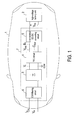
- FIG 1 is a schematic circuit block diagram illustrating the architecture of a high-voltage battery charging system according to an embodiment of the present invention
- FIG 2 is a schematic detailed circuit block diagram illustrating the architecture of a high-voltage battery charging system according to an embodiment of the present invention
- FIG 3 is a schematic detailed circuit block diagram illustrating the architecture of another high-voltage battery charging system according to an embodiment of the present invention.
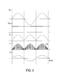
- FIG 4 is a timing waveform diagram schematically illustrating the corresponding voltage signals and current signals processed in the high-voltage battery charging system of FIGS. 2 and 3 ;
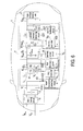
- FIG 5 is a schematic detailed circuit block diagram illustrating the architecture of another high-voltage battery charging system according to a further embodiment of the present invention.
- FIG 6 is a schematic detailed circuit block diagram illustrating the architecture of another high-voltage battery charging system according to a further embodiment of the present invention.
- FIG 1 is a schematic circuit block diagram illustrating the architecture of a high-voltage battery charging system according to an embodiment of the present invention.
- the high-voltage battery charging system is installed in an electric vehicle body 1.
- the high-voltage battery charging system is used for receiving electric energy of an AC input voltage V in from an utility power source, and charging a high-voltage battery unit 2.
- the high-voltage battery charging system comprises a rectifier circuit 3, a power factor correction (PFC) circuit 4, a non-isolated DC-DC converting circuit 5 and a bus capacitor C bus .
- PFC power factor correction
- the high-voltage battery charging system further comprises an electromagnetic interference (EMI) filtering circuit 6.
- the EMI filtering circuit 6 is connected to the input side of the rectifier circuit 3 for filtering off the surge and high-frequency noise contained in the AC input voltage V in and the AC input current I in .
- the use of the EMI filtering circuit 6 can reduce the electromagnetic interference resulted from the switching circuits of the non-isolated DC-DC converting circuit 5 and the PFC circuit 4, so that the adverse influence of the electromagnetic interference on the AC input voltage V in and the AC input current I in will be minimized.
- the AC input voltage V in and the AC input current I in are transmitted to the input side of the rectifier circuit 3.
- the AC input voltage V in is rectified into a rectified voltage V r by the rectifier circuit 3.
- the PFC circuit 4 is interconnected between the rectifier circuit 3 and a bus B 1 for increasing the power factor and generating a bus voltage V bus .
- the non-isolated DC-DC converting circuit 5 is interconnected between the PFC circuit 4 and the high-voltage battery unit 2 for converting the bus voltage V bus into a charging voltage V Hb .
- the high-voltage battery unit 2 is charged by the charging voltage V Hb .
- the bus capacitor C bus is interconnected between the bus B 1 and a common terminal COM for energy storage and voltage stabilization.
- no transformer is included in the electric energy path of the non-isolated DC-DC converting circuit 5.
- the high-voltage battery unit 2 is charged by the charging voltage V Hb .
- the magnitude of the AC input voltage V in is 110 ⁇ 380 volts
- the magnitude of the bus voltage V bus is 350 ⁇ 450 volts
- the magnitude of the charging voltage V Hb is 200 ⁇ 380 volts.
- the rectifier circuit 3, the PFC circuit 4, the non-isolated DC-DC converting circuit 5, the EMI filtering circuit 6 and the bus capacitor C bus of the high-voltage battery charging system 7 and the high-voltage battery unit 2 are operated at high voltage values.
- the high-voltage battery charging system 7 has low charging loss and short charging time during the charging process and has low power loss and enhanced efficiency during the driving process.
- voltage values of the high-voltage battery charging system 7 and the high-voltage battery unit 2 are higher than the safety extra-low voltage (e.g.
- a high voltage-resistant insulating material is used to separate or isolate the high-voltage battery charging system 7 and the high-voltage battery unit 2 from the electric vehicle body 1 where the driver or passengers is touchable.
- the high-voltage battery charging system 7 and the high-voltage battery unit 2 are separated from the electric vehicle body 1 by at least a specified safety distance (e.g. 3 ⁇ 8mm, 5mm, 6mm, 6.5mm, 7mm, 9mm or 12mm).
- the high-voltage battery charging system 7 and the high-voltage battery unit 2 are contained in respective insulated containers.
- the high-voltage battery charging system 7 is connected with the high-voltage battery unit 2 and the utility power source via high voltage-resistant cables with insulating covering (not shown).
- the charging voltage V Hb and the AC input voltage V in are respectively transmitted to the high-voltage battery unit 2 and the high-voltage battery charging system 7 through the high voltage-resistant cables.
- the surface of the electric vehicle body 1 is coated with a high voltage-resistant insulating material (e.g. an insulating varnish) or an insulating spacer is disposed at the contact region between the electric vehicle body 1, the high-voltage battery charging system 7 and the high-voltage battery unit 2.
- a high voltage-resistant insulating material e.g. an insulating varnish
- an insulating spacer is disposed at the contact region between the electric vehicle body 1, the high-voltage battery charging system 7 and the high-voltage battery unit 2.
- An example of the non-isolated DC-DC converting circuit 5 includes but is not limited to a buck non-isolated DC-DC converting circuit, a buck-boost non-isolated DC-DC converting circuit or a boost non-isolated DC-DC converting circuit.
- An example of the PFC circuit 4 includes but is not limited to a continuous conduction mode (CCM) boost PFC circuit, a direct coupling modulated bias (DCMB) boost PFC circuit, a buck PFC circuit or a buck-boost PFC circuit.
- the high-voltage battery unit 2 includes one or more batteries such as lead-acid batteries, nickel-cadmium batteries, nickel iron batteries, nickel-metal hydride batteries, lithium-ion batteries, or a combination thereof.
- FIG 2 is a schematic detailed circuit block diagram illustrating the architecture of a high-voltage battery charging system according to an embodiment of the present invention.
- the PFC circuit 4 comprises a first inductor L 1 , a first diode D 1 (a first rectifier element), a first switching circuit 41, a first current-detecting circuit 42 and a power factor correction controlling unit 43.
- a first terminal of the first inductor L 1 is connected to a positive output terminal of the rectifier circuit 3.
- a second terminal of first inductor L 1 is connected to a first connecting node K 1 .
- the first switching circuit 41 and the first current-detecting circuit 42 are serially connected between the first connecting node K 1 and the common terminal COM.
- the anode of the first diode D 1 is connected to the first connecting node K 1 .
- the cathode of the first diode D 1 is connected to the bus B 1 .
- the power factor correction controlling unit 43 is connected to the common terminal COM, the positive output terminal of the rectifier circuit 3, the bus B 1 , the control terminal of the first switching circuit 41 and the first current-detecting circuit 42.
- the power factor correction controlling unit 43 is used for controlling operations of the PFC circuit 4.
- the first inductor L 1 In a case that the first switching circuit 41 is conducted, the first inductor L 1 is in a charge status and the current magnitude of the first current I 1 is increased. The first current I 1 will be transmitted from the first inductor L 1 to the first current-detecting circuit 42 through the first switching circuit 41, so that a current-detecting signal V s is generated by the first current-detecting circuit 42. Whereas, in a case that the first switching circuit 41 is shut off, the first inductor L 1 is in a discharge status and the current magnitude of the first current I 1 is decreased. The first current I 1 will be transmitted to the bus capacitor C bus through the first diode D 1 .
- the power factor correction controlling unit 43 comprises an input waveform detecting circuit 431, a first feedback circuit 432 and a power factor correction controller 433.
- the input waveform detecting circuit 431 is connected to the positive input terminal of the rectifier circuit 3, the power factor correction controller 433 and the common terminal COM.
- the input waveform detecting circuit 431 is used for reducing the voltage magnitude of the rectified voltage V r and filtering off the high-frequency noise contained in the rectified voltage V r , thereby generating an input detecting signal V ra .
- the waveform of the input detecting signal V ra is identical to that of the AC input voltage V in after being rectified.
- the first feedback circuit 432 is connected to the bus B1 the power factor correction controller 433 and the common terminal COM.
- the bus voltage V bus is subject to voltage-division by the first feedback circuit 432, thereby generating a first feedback signal V fl .
- the power factor correction controller 433 acquires the waveform of the AC input voltage V in by the detecting signal V ra .
- the power factor correction controller 433 discriminates whether the bus voltage V bus is maintained at the rated voltage value (e.g. 450V) by the first feedback signal V fl .
- the increase magnitude of the first current I 1 is detected by the current-detecting signal V s .
- the power factor correction controller 433 controls the duty cycle of the first switching circuit 41.
- the bus voltage V bus is maintained at the rated voltage value, and the distribution of the AC input current I in is similar to the waveform of the AC input voltage V in .
- the distribution of the first current I 1 is similar to the waveform of the AC input voltage V in after being rectified.
- the envelop curve E1 of the first current I 1 illustrates a dotted line enclosing the periphery of the waveform of the AC input current I in .
- the envelop curve of the AC input current I in is similar to the waveform of the AC input voltage V in.
- the phase of the AC input current I in is similar to that of the AC input voltage V in . Under this circumstance, a better power factor correction function is achieved.
- the non-isolated DC-DC converting circuit 5 is a single-phase non-isolated DC-DC converting circuit.
- the non-isolated DC-DC converting circuit 5 comprises a second inductor L 2 , a second diode D 2 (a second rectifier element), a first output capacitor C o1 , a second switching circuit 51 a and a DC-DC controlling unit 52.
- the second inductor L 2 , the second diode D 2 (a second rectifier element), the first output capacitor C 01 and the second switching circuit 51 a define a first phase power circuit.
- the second inductor L 2 is interconnected between a second connecting node K 2 and the high-voltage battery unit 2.
- the second diode D 2 is interconnected between the second connecting node K 2 and the common terminal COM.
- the first output capacitor C 01 is interconnected between the high-voltage battery unit 2 and the common terminal COM.
- the second switching circuit 51 a is interconnected between the bus B 1 and the second connecting node K 2 .
- the DC-DC controlling unit 52 is connected to the control terminal of the second switching circuit 51a, the common terminal COM and the high-voltage battery unit 2. According to the charging voltage VH b, the on/off statuses of the second switching circuit 51a are controlled by the DC-DC controlling unit 52.
- the DC-DC controlling unit 52 comprises a second feedback circuit 521 and a DC-DC controller 522.
- the second feedback circuit 521 is connected to the high-voltage battery unit 2, the DC-DC controller 522 and the common terminal COM.
- the charging voltage V Hb is subject to voltage-division by the second feedback circuit 521, thereby generating a second feedback signal V f2 .
- the DC-DC controller 522 is connected to the control terminal of the second switching circuit 51 a, the second feedback circuit 521 and the common terminal COM. According to the second feedback signal V f2 , the DC-DC controller 522 discriminates whether the charging voltage V Hb is maintained at the rated voltage value (e.g. 380V). As a consequence, the duty cycle of the second switching circuit 51 a is controlled, and the charging voltage V Hb is maintained at the rated voltage value.
- the rated voltage value e.g. 380V
- the electric energy path of the non-isolated DC-DC converting circuit 5 passes through the second switching circuit 51 a and the second inductor L 2 . In other words, no transformer is included in the non-isolated DC-DC converting circuit 5.
- a first output filter circuit is defined by the second inductor L 2 and the first output capacitor Co 1 .
- the operations of the first output filter circuit and the second switching circuit 51 a cause the high-voltage battery unit 2 to be charged by the charging voltage V Hb . That is, by the switching circuit and the output filter circuit of the non-isolated DC-DC converting circuit 5, the high-voltage battery unit 2 is charged by the charging voltage V Hb .
- FIG 3 is a schematic detailed circuit block diagram illustrating the architecture of another high-voltage battery charging system according to an embodiment of the present invention.
- the non-isolated DC-DC converting circuit 5 of FIG 3 is a multi-phase non-isolated DC-DC converting circuit.
- the non-isolated DC-DC converting circuit 5 of FIG 3 further comprises a second phase power circuit.
- the second inductor L 2 , the second diode D 2 (a second rectifier element), the first output capacitor Co 1 and the second switching circuit 51 a collectively define the first phase power circuit.
- a third inductor L 3 , a third diode D 3 (a third rectifier element), a third output capacitor C 02 and a third switching circuit 51b collectively define the second phase power circuit.
- the second phase power circuit is connected with the first phase power circuit is parallel.
- the third inductor L 3 is interconnected between a third connecting node K 3 and the high-voltage battery unit 2.
- the third diode D 3 is interconnected between the third connecting node K 3 and the common terminal COM.
- the second output capacitor Co 2 is interconnected between the high-voltage battery unit 2 and the common terminal COM.
- the third switching circuit 51b is interconnected between the bus B, and the third connecting node K 3 .
- the DC-DC controlling unit 52 is connected to the control terminal of the second switching circuit 51a, the control terminal of the third switching circuit 51 b, the common terminal COM and the high-voltage battery unit 2. According to the charging voltage V Hb , the second switching circuit 51 a and the third switching circuit 51 b are alternately conducted under control of the DC-DC controlling unit 52. As a consequence, the duty cycles of the second switching circuit 51a and the third switching circuit 51b are controlled, and the charging voltage V Hb is maintained at the rated voltage value.
- the high-voltage battery charging system 7 since the non-isolated DC-DC converting circuit 5 is a multi-phase converting circuit, the high-voltage battery charging system 7 has enhanced operating efficiency and enhanced heat dissipating efficiency when the high-voltage battery charging system 7 is applied to an electric vehicle having higher charging power (e.g. 1000 or 2000 Watts).
- higher charging power e.g. 1000 or 2000 Watts.
- the rectifier circuit 3 is a bridge rectifier circuit.
- the positive output terminal of the rectifier circuit 3 is connected to the input terminal of the power factor correction circuit 4.
- the negative output terminal of the rectifier circuit 3 is connected to the common terminal COM.
- An example of the first current-detecting circuit 42 includes but is not limited to a current transformer or a detecting resistor R S .
- Each of the first switching circuit 41, the second switching circuit 51 a and the third switching circuit 51 b includes one or more switch elements.
- the switch element is a metal oxide semiconductor field effect transistor (MOSFET), a bipolar junction transistor (BJT) or an insulated gate bipolar transistor (IGBT).
- MOSFET metal oxide semiconductor field effect transistor
- BJT bipolar junction transistor
- IGBT insulated gate bipolar transistor
- each of the first switching circuit 41, the second switching circuit 51a and the third switching circuit 51b includes a metal oxide semiconductor field effect transistor (MOSFET).
- MOSFET metal oxide semiconductor field effect transistor
- Each of the power factor correction controller 433 and the DC-DC controller 522 includes a controller, a micro controller unit (MCU) or a digital signal processor (DSP).
- FIG 4 is a timing waveform diagram schematically illustrating the corresponding voltage signals and current signals processed in the high-voltage battery charging system of FIGS. 2 and 3 .
- the first current I 1 is increased or decreased as the first switching circuit 41 is conducted or shut off.
- the distribution of the first current I 1 is similar to the waveform of the AC input voltage V in after being rectified.
- the envelop curve E1 of the first current I 1 is similar to the waveform of the AC input voltage V in .
- the waveform of the AC input current I in indicates that the AC input current I in is not rectified and the surge and high-frequency noise contained in the AC input current I in has been filtered off by the EMI filtering circuit 6.
- the electromagnetic interference resulted from the switching circuits of the non-isolated DC-DC converting circuit 5 and the PFC circuit 4 is minimized.
- the distribution of the AC input current I in is similar to the waveform of the AC input voltage V in .
- the envelop curve of the AC input current I in is similar to the waveform of the AC input voltage V in .
- the phase of the AC input current I in is similar to that of the AC input voltage V in . Since the phase difference is very low (e.g. 1 ⁇ 15 degrees), a better power factor correction function is achieved.
- FIG 5 is a schematic detailed circuit block diagram illustrating the architecture of another high-voltage battery charging system according to a further embodiment of the present invention.
- the high-voltage battery charging system of FIG 5 further comprises an auxiliary power circuit 8.
- the power input terminal of the auxiliary power circuit 8 is connected to the bus B1.
- the power output terminal of the auxiliary power circuit 8 is connected to the power factor correction controlling unit 43 and the DC-DC controlling unit 52 for converting the bus voltage V bus into an auxiliary voltage V a , thereby providing the electric energy required for operating the power factor correction controlling unit 43 and the DC-DC controlling unit 52.
- the power output terminal of the auxiliary power circuit 8 is connected to the power factor correction controller 433 and the DC-DC controller 522.
- the auxiliary power circuit 8 is connected to the input waveform detecting circuit 431, the first feedback circuit 432 and the second feedback circuit 521 to provide electric energy to the input waveform detecting circuit 431, the first feedback circuit 432 and the second feedback circuit 521 (not shown). Since the auxiliary power circuit 8 receives the bus voltage V bus rather than the AC input voltage V in , the overall power factor of the integrated circuit is not adversely affected by the auxiliary power circuit 8 and thus a stable auxiliary voltage V a is achievable.
- FIG 6 is a schematic detailed circuit block diagram illustrating the architecture of another high-voltage battery charging system according to a further embodiment of the present invention.
- the high-voltage battery charging system further comprises a second current-detecting circuit 523.
- the second current-detecting circuit 523 is used for sampling the current signal outputted from the non-isolated DC-DC converting circuit 5, detecting the current flowing through the second inductor L 2 of the non-isolated DC-DC converting circuit 5, or detecting the current flowing through the second switching circuit 51 a and the second diode D 2 .
- the second inductor L 2 of the non-isolated DC-DC converting circuit 5 is shown. The other currents may be detected by the similar approaches.
- the DC-DC controlling unit 52 of the non-isolated DC-DC converting circuit 5 of FIG 6 further comprises the second current-detecting circuit 523.
- the second current-detecting circuit 523 is connected to the second inductor L 2 and the DC-DC controller 522 for sampling the current signal outputted from the non-isolated DC-DC converting circuit 5.
- the output current is replaced by the current flowing through the second inductor L 2 .
- the high-voltage battery unit 2 is charged by the non-isolated DC-DC converting circuit 5 with a constant voltage.
- the duty cycle of the second switching circuit 51 a could be determined by the DC-DC controlling unit 52.
- the high-voltage battery unit 2 could be charged by the non-isolated DC-DC converting circuit 5 with a constant current.
- the duty cycle of the second switching circuit 51 a is determined by the DC-DC controlling unit 52 according to the current of the second inductor L 2 detected by the second current-detecting circuit 523 or the output voltage acquired by the second feedback circuit 521.
- the high-voltage battery unit 2 could be charged by the non-isolated DC-DC converting circuit 5 with constant power. That is, the high-voltage battery unit 2 could be charged with constant charging current or constant charging power.
- the second current-detecting circuit 523 could discriminate whether the charging current exceeds a threshold value. Under control of the DC-DC controller 522, the duty cycle of the second switching circuit 51a is reduced or the second switching circuit 51 a is disabled. As a consequence, the possibility of burning out the non-isolated DC-DC converting circuit 5 is minimized.
Landscapes
- Engineering & Computer Science (AREA)
- Power Engineering (AREA)
- Transportation (AREA)
- Mechanical Engineering (AREA)
- Life Sciences & Earth Sciences (AREA)
- Sustainable Development (AREA)
- Sustainable Energy (AREA)
- Charge And Discharge Circuits For Batteries Or The Like (AREA)
- Electric Propulsion And Braking For Vehicles (AREA)
- Secondary Cells (AREA)
- Dc-Dc Converters (AREA)
Abstract
A high-voltage battery charging system is installed in a vehicle body of the electric vehicle for charging a high-voltage battery unit within the vehicle body. The high-voltage battery charging system includes a rectifier circuit, a power factor correction circuit and a non-isolated DC-DC converting circuit. The rectifier circuit is connected to a common terminal for rectifying an AC input voltage into a rectified voltage. The power factor correction circuit is connected to the rectifier circuit and a bus for increasing a power factor and generating a bus voltage. The non-isolated DC-DC converting circuit is connected to the power factor correction circuit and the high-voltage battery unit for charging the high-voltage battery unit, wherein no transformer is included in the non-isolated DC-DC converting circuit.
Description
- The present invention relates to a high-voltage battery charging system, and more particularly to a high-voltage battery charging system for use in an electric vehicle.
- Fossil fuels such as petroleum and coal are widely used in automobiles or power plants for generating motive force or electrical power. As known, burning fossil fuels produces waste gases and carbon oxide. The waste gases may pollute the air. In addition, carbon dioxide is considered to be a major cause of the enhanced greenhouse effect. It is estimated that the world's oils supply would be depleted in the next several decades. The oil depletion may lead to global economic crisis.
- Consequently, there are growing demands on clean and renewable energy. Recently, electric vehicles and plug-in hybrid electric vehicles have been researched and developed. Electric vehicles and plug-in hybrid electric vehicles use electrical generators to generate electricity. In comparison with the conventional gasoline vehicles and diesel vehicles, the electric vehicles and hybrid electric vehicles are advantageous because of low pollution, low noise and better energy utilization. The uses of the electric vehicles and hybrid electric vehicles can reduce carbon dioxide release in order to decelerate the greenhouse effect.
- As known, an electric vehicle or a plug-in hybrid electric vehicle has a built-in battery as a stable energy source for providing electric energy for powering the vehicle. In a case that the electric energy stored in the battery is exhausted, the battery is usually charged by a battery charger. Generally, the current battery charger has an isolated architecture, and a transformer is an essential component in an electric energy path of an isolated DC-DC converter. During the process of converting electric energy by the transformer, magnetic loss (iron loss) and wire loss (copper loss) are incurred. That is, the power loss of the isolated DC-DC converter is very high. In this situation, the charging time of the battery is long. Moreover, since an insulating tape or a three-layered insulating wire is required for isolating the primary winding from the secondary winding of the transformer, the process of fabricating the transformer is complicated and costly.
- Therefore, there is a need of providing a high-voltage battery charging system for use in an electric vehicle so as to obviate the drawbacks encountered from the prior art.
- It is an object of the present invention to provide a high-voltage battery charging system for use in an electric vehicle in order to reduce power loss, reduce the fabricating cost, shorten the charging time, and increase the operating efficiency.
- In accordance with an aspect of the present invention, there is provided a high-voltage battery charging system for use in an electric vehicle. The high-voltage battery charging system is installed in a vehicle body of the electric vehicle for charging a high-voltage battery unit within the vehicle body. The high-voltage battery charging system includes a rectifier circuit, a power factor correction circuit and a non-isolated DC-DC converting circuit. The rectifier circuit is connected to a common terminal for rectifying an AC input voltage into a rectified voltage. The power factor correction circuit is connected to the rectifier circuit and a bus for increasing a power factor and generating a bus voltage. The non-isolated DC-DC converting circuit is connected to the power factor correction circuit and the high-voltage battery unit for charging the high-voltage battery unit, wherein no transformer is included in the non-isolated DC-DC converting circuit.
- The above contents of the present invention will become more readily apparent to those ordinarily skilled in the art after reviewing the following detailed description and accompanying drawings, in which:
-
FIG 1 is a schematic circuit block diagram illustrating the architecture of a high-voltage battery charging system according to an embodiment of the present invention; -
FIG 2 is a schematic detailed circuit block diagram illustrating the architecture of a high-voltage battery charging system according to an embodiment of the present invention; -
FIG 3 is a schematic detailed circuit block diagram illustrating the architecture of another high-voltage battery charging system according to an embodiment of the present invention; -
FIG 4 is a timing waveform diagram schematically illustrating the corresponding voltage signals and current signals processed in the high-voltage battery charging system ofFIGS. 2 and3 ; -
FIG 5 is a schematic detailed circuit block diagram illustrating the architecture of another high-voltage battery charging system according to a further embodiment of the present invention; and -
FIG 6 is a schematic detailed circuit block diagram illustrating the architecture of another high-voltage battery charging system according to a further embodiment of the present invention. - The present invention will now be described more specifically with reference to the following embodiments. It is to be noted that the following descriptions of preferred embodiments of this invention are presented herein for purpose of illustration and description only. It is not intended to be exhaustive or to be limited to the precise form disclosed.
-
FIG 1 is a schematic circuit block diagram illustrating the architecture of a high-voltage battery charging system according to an embodiment of the present invention. The high-voltage battery charging system is installed in anelectric vehicle body 1. The high-voltage battery charging system is used for receiving electric energy of an AC input voltage Vin from an utility power source, and charging a high-voltage battery unit 2. As shown inFIG 1 , the high-voltage battery charging system comprises arectifier circuit 3, a power factor correction (PFC)circuit 4, a non-isolated DC-DC converting circuit 5 and a bus capacitor Cbus. - In this embodiment, the high-voltage battery charging system further comprises an electromagnetic interference (EMI)
filtering circuit 6. TheEMI filtering circuit 6 is connected to the input side of therectifier circuit 3 for filtering off the surge and high-frequency noise contained in the AC input voltage V in and the AC input current Iin. In addition, the use of theEMI filtering circuit 6 can reduce the electromagnetic interference resulted from the switching circuits of the non-isolated DC-DC converting circuit 5 and thePFC circuit 4, so that the adverse influence of the electromagnetic interference on the AC input voltage Vin and the AC input current Iin will be minimized. After the surge and high-frequency noise are filtered off by theEMI filtering circuit 6, the AC input voltage Vin and the AC input current Iin are transmitted to the input side of therectifier circuit 3. The AC input voltage Vin is rectified into a rectified voltage Vr by therectifier circuit 3. - The
PFC circuit 4 is interconnected between therectifier circuit 3 and a bus B1 for increasing the power factor and generating a bus voltage Vbus. The non-isolated DC-DC converting circuit 5 is interconnected between thePFC circuit 4 and the high-voltage battery unit 2 for converting the bus voltage Vbus into a charging voltage VHb. The high-voltage battery unit 2 is charged by the charging voltage VHb. The bus capacitor Cbus is interconnected between the bus B1 and a common terminal COM for energy storage and voltage stabilization. In accordance with a key feature of the present invention, no transformer is included in the electric energy path of the non-isolated DC-DC converting circuit 5. By mean of a switching circuit and an output filter circuit of the non-isolated DC-DC converting circuit 5, the high-voltage battery unit 2 is charged by the charging voltage VHb. - In this embodiment, the magnitude of the AC input voltage Vin is 110~380 volts, the magnitude of the bus voltage Vbus is 350~450 volts, and the magnitude of the charging voltage VHb is 200~380 volts. The
rectifier circuit 3, thePFC circuit 4, the non-isolated DC-DC converting circuit 5, theEMI filtering circuit 6 and the bus capacitor Cbus of the high-voltagebattery charging system 7 and the high-voltage battery unit 2 are operated at high voltage values. As such, the high-voltagebattery charging system 7 has low charging loss and short charging time during the charging process and has low power loss and enhanced efficiency during the driving process. Generally, voltage values of the high-voltagebattery charging system 7 and the high-voltage battery unit 2 are higher than the safety extra-low voltage (e.g. 36V). For preventing the AC input voltage Vin the bus voltage Vbus or the charging voltage VHb from attacking the driver or passengers within theelectric vehicle body 1, a high voltage-resistant insulating material is used to separate or isolate the high-voltagebattery charging system 7 and the high-voltage battery unit 2 from theelectric vehicle body 1 where the driver or passengers is touchable. Alternatively, the high-voltagebattery charging system 7 and the high-voltage battery unit 2 are separated from theelectric vehicle body 1 by at least a specified safety distance (e.g. 3~8mm, 5mm, 6mm, 6.5mm, 7mm, 9mm or 12mm). - In an embodiment, the high-voltage
battery charging system 7 and the high-voltage battery unit 2 are contained in respective insulated containers. In addition, the high-voltagebattery charging system 7 is connected with the high-voltage battery unit 2 and the utility power source via high voltage-resistant cables with insulating covering (not shown). As such, the charging voltage VHb and the AC input voltage Vin are respectively transmitted to the high-voltage battery unit 2 and the high-voltagebattery charging system 7 through the high voltage-resistant cables. - In some embodiments, for protecting the driver or passengers, the surface of the
electric vehicle body 1 is coated with a high voltage-resistant insulating material (e.g. an insulating varnish) or an insulating spacer is disposed at the contact region between theelectric vehicle body 1, the high-voltagebattery charging system 7 and the high-voltage battery unit 2. - An example of the non-isolated DC-
DC converting circuit 5 includes but is not limited to a buck non-isolated DC-DC converting circuit, a buck-boost non-isolated DC-DC converting circuit or a boost non-isolated DC-DC converting circuit. An example of thePFC circuit 4 includes but is not limited to a continuous conduction mode (CCM) boost PFC circuit, a direct coupling modulated bias (DCMB) boost PFC circuit, a buck PFC circuit or a buck-boost PFC circuit. The high-voltage battery unit 2 includes one or more batteries such as lead-acid batteries, nickel-cadmium batteries, nickel iron batteries, nickel-metal hydride batteries, lithium-ion batteries, or a combination thereof. -
FIG 2 is a schematic detailed circuit block diagram illustrating the architecture of a high-voltage battery charging system according to an embodiment of the present invention. As shown inFIG 2 , thePFC circuit 4 comprises a first inductor L1, a first diode D1 (a first rectifier element), afirst switching circuit 41, a first current-detectingcircuit 42 and a power factorcorrection controlling unit 43. A first terminal of the first inductor L1 is connected to a positive output terminal of therectifier circuit 3. A second terminal of first inductor L1 is connected to a first connecting node K1. Thefirst switching circuit 41 and the first current-detectingcircuit 42 are serially connected between the first connecting node K1 and the common terminal COM. The anode of the first diode D1 is connected to the first connecting node K1. The cathode of the first diode D1 is connected to the bus B1. The power factorcorrection controlling unit 43 is connected to the common terminal COM, the positive output terminal of therectifier circuit 3, the bus B1, the control terminal of thefirst switching circuit 41 and the first current-detectingcircuit 42. The power factorcorrection controlling unit 43 is used for controlling operations of thePFC circuit 4. - In a case that the
first switching circuit 41 is conducted, the first inductor L1 is in a charge status and the current magnitude of the first current I1 is increased. The first current I1 will be transmitted from the first inductor L1 to the first current-detectingcircuit 42 through thefirst switching circuit 41, so that a current-detecting signal Vs is generated by the first current-detectingcircuit 42. Whereas, in a case that thefirst switching circuit 41 is shut off, the first inductor L1 is in a discharge status and the current magnitude of the first current I1 is decreased. The first current I1 will be transmitted to the bus capacitor Cbus through the first diode D1. - In this embodiment, the power factor
correction controlling unit 43 comprises an inputwaveform detecting circuit 431, afirst feedback circuit 432 and a powerfactor correction controller 433. The inputwaveform detecting circuit 431 is connected to the positive input terminal of therectifier circuit 3, the powerfactor correction controller 433 and the common terminal COM. The inputwaveform detecting circuit 431 is used for reducing the voltage magnitude of the rectified voltage Vr and filtering off the high-frequency noise contained in the rectified voltage Vr, thereby generating an input detecting signal Vra. The waveform of the input detecting signal Vra is identical to that of the AC input voltage Vin after being rectified. Thefirst feedback circuit 432 is connected to the bus B1 the powerfactor correction controller 433 and the common terminal COM. The bus voltage Vbus is subject to voltage-division by thefirst feedback circuit 432, thereby generating a first feedback signal Vfl. - In other words, the power
factor correction controller 433 acquires the waveform of the AC input voltage Vin by the detecting signal Vra. The powerfactor correction controller 433 discriminates whether the bus voltage Vbus is maintained at the rated voltage value (e.g. 450V) by the first feedback signal Vfl. The increase magnitude of the first current I1 is detected by the current-detecting signal Vs. According to the detecting signal Vra, Vf1, and Vs, the powerfactor correction controller 433 controls the duty cycle of thefirst switching circuit 41. As a consequence, the bus voltage Vbus is maintained at the rated voltage value, and the distribution of the AC input current Iin is similar to the waveform of the AC input voltage Vin. The distribution of the first current I1 is similar to the waveform of the AC input voltage Vin after being rectified. As shown inFIG 4 , the envelop curve E1 of the first current I1 illustrates a dotted line enclosing the periphery of the waveform of the AC input current Iin. After the AC input current Iin is processed by theEMI filtering circuit 6, the envelop curve of the AC input current Iin is similar to the waveform of the AC input voltage Vin. In addition, the phase of the AC input current Iin is similar to that of the AC input voltage Vin. Under this circumstance, a better power factor correction function is achieved. - In this embodiment, the non-isolated DC-
DC converting circuit 5 is a single-phase non-isolated DC-DC converting circuit. The non-isolated DC-DC converting circuit 5 comprises a second inductor L2, a second diode D2 (a second rectifier element), a first output capacitor Co1, asecond switching circuit 51 a and a DC-DC controlling unit 52. The second inductor L2, the second diode D2 (a second rectifier element), the first output capacitor C01 and thesecond switching circuit 51 a define a first phase power circuit. The second inductor L2 is interconnected between a second connecting node K2 and the high-voltage battery unit 2. The second diode D2 is interconnected between the second connecting node K2 and the common terminal COM. The first output capacitor C01 is interconnected between the high-voltage battery unit 2 and the common terminal COM. Thesecond switching circuit 51 a is interconnected between the bus B1 and the second connecting node K2. The DC-DC controlling unit 52 is connected to the control terminal of thesecond switching circuit 51a, the common terminal COM and the high-voltage battery unit 2. According to the charging voltage VHb, the on/off statuses of thesecond switching circuit 51a are controlled by the DC-DC controlling unit 52. - In this embodiment, the DC-
DC controlling unit 52 comprises asecond feedback circuit 521 and a DC-DC controller 522. Thesecond feedback circuit 521 is connected to the high-voltage battery unit 2, the DC-DC controller 522 and the common terminal COM. The charging voltage VHb is subject to voltage-division by thesecond feedback circuit 521, thereby generating a second feedback signal Vf2. The DC-DC controller 522 is connected to the control terminal of thesecond switching circuit 51 a, thesecond feedback circuit 521 and the common terminal COM. According to the second feedback signal Vf2, the DC-DC controller 522 discriminates whether the charging voltage VHb is maintained at the rated voltage value (e.g. 380V). As a consequence, the duty cycle of thesecond switching circuit 51 a is controlled, and the charging voltage VHb is maintained at the rated voltage value. - The electric energy path of the non-isolated DC-
DC converting circuit 5 passes through thesecond switching circuit 51 a and the second inductor L2. In other words, no transformer is included in the non-isolated DC-DC converting circuit 5. In the non-isolated DC-DC converting circuit 5, a first output filter circuit is defined by the second inductor L2 and the first output capacitor Co1. The operations of the first output filter circuit and thesecond switching circuit 51 a cause the high-voltage battery unit 2 to be charged by the charging voltage VHb. That is, by the switching circuit and the output filter circuit of the non-isolated DC-DC converting circuit 5, the high-voltage battery unit 2 is charged by the charging voltage VHb. -
FIG 3 is a schematic detailed circuit block diagram illustrating the architecture of another high-voltage battery charging system according to an embodiment of the present invention. In comparison withFIG 2 , the non-isolated DC-DC converting circuit 5 ofFIG 3 is a multi-phase non-isolated DC-DC converting circuit. In addition to the first phase power circuit and the DC-DC controlling unit 52, the non-isolated DC-DC converting circuit 5 ofFIG 3 further comprises a second phase power circuit. The second inductor L2, the second diode D2 (a second rectifier element), the first output capacitor Co1 and thesecond switching circuit 51 a collectively define the first phase power circuit. A third inductor L3, a third diode D3 (a third rectifier element), a third output capacitor C02 and athird switching circuit 51b collectively define the second phase power circuit. The second phase power circuit is connected with the first phase power circuit is parallel. - The third inductor L3 is interconnected between a third connecting node K3 and the high-
voltage battery unit 2. The third diode D3 is interconnected between the third connecting node K3 and the common terminal COM. The second output capacitor Co2 is interconnected between the high-voltage battery unit 2 and the common terminal COM. Thethird switching circuit 51b is interconnected between the bus B, and the third connecting node K3. The DC-DC controlling unit 52 is connected to the control terminal of thesecond switching circuit 51a, the control terminal of thethird switching circuit 51 b, the common terminal COM and the high-voltage battery unit 2. According to the charging voltage VHb, thesecond switching circuit 51 a and thethird switching circuit 51 b are alternately conducted under control of the DC-DC controlling unit 52. As a consequence, the duty cycles of thesecond switching circuit 51a and thethird switching circuit 51b are controlled, and the charging voltage VHb is maintained at the rated voltage value. - In this embodiment, since the non-isolated DC-
DC converting circuit 5 is a multi-phase converting circuit, the high-voltagebattery charging system 7 has enhanced operating efficiency and enhanced heat dissipating efficiency when the high-voltagebattery charging system 7 is applied to an electric vehicle having higher charging power (e.g. 1000 or 2000 Watts). - In the above embodiments, the
rectifier circuit 3 is a bridge rectifier circuit. The positive output terminal of therectifier circuit 3 is connected to the input terminal of the powerfactor correction circuit 4. The negative output terminal of therectifier circuit 3 is connected to the common terminal COM. An example of the first current-detectingcircuit 42 includes but is not limited to a current transformer or a detecting resistor RS. Each of thefirst switching circuit 41, thesecond switching circuit 51 a and thethird switching circuit 51 b includes one or more switch elements. The switch element is a metal oxide semiconductor field effect transistor (MOSFET), a bipolar junction transistor (BJT) or an insulated gate bipolar transistor (IGBT). In this embodiment, each of thefirst switching circuit 41, thesecond switching circuit 51a and thethird switching circuit 51b includes a metal oxide semiconductor field effect transistor (MOSFET). Each of the powerfactor correction controller 433 and the DC-DC controller 522 includes a controller, a micro controller unit (MCU) or a digital signal processor (DSP). -
FIG 4 is a timing waveform diagram schematically illustrating the corresponding voltage signals and current signals processed in the high-voltage battery charging system ofFIGS. 2 and3 . As shown inFIG 4 , the first current I1 is increased or decreased as thefirst switching circuit 41 is conducted or shut off. The distribution of the first current I1 is similar to the waveform of the AC input voltage Vin after being rectified. The envelop curve E1 of the first current I1 is similar to the waveform of the AC input voltage Vin. - The waveform of the AC input current Iin indicates that the AC input current Iin is not rectified and the surge and high-frequency noise contained in the AC input current Iin has been filtered off by the
EMI filtering circuit 6. In this embodiment, the electromagnetic interference resulted from the switching circuits of the non-isolated DC-DC converting circuit 5 and thePFC circuit 4 is minimized. The distribution of the AC input current Iin is similar to the waveform of the AC input voltage Vin. The envelop curve of the AC input current Iin is similar to the waveform of the AC input voltage Vin. The phase of the AC input current Iin is similar to that of the AC input voltage Vin. Since the phase difference is very low (e.g. 1~15 degrees), a better power factor correction function is achieved. -
FIG 5 is a schematic detailed circuit block diagram illustrating the architecture of another high-voltage battery charging system according to a further embodiment of the present invention. In comparison withFIG 2 , the high-voltage battery charging system ofFIG 5 further comprises an auxiliary power circuit 8. The power input terminal of the auxiliary power circuit 8 is connected to the bus B1. The power output terminal of the auxiliary power circuit 8 is connected to the power factorcorrection controlling unit 43 and the DC-DC controlling unit 52 for converting the bus voltage Vbus into an auxiliary voltage Va, thereby providing the electric energy required for operating the power factorcorrection controlling unit 43 and the DC-DC controlling unit 52. In this embodiment, the power output terminal of the auxiliary power circuit 8 is connected to the powerfactor correction controller 433 and the DC-DC controller 522. In some embodiments, the auxiliary power circuit 8 is connected to the inputwaveform detecting circuit 431, thefirst feedback circuit 432 and thesecond feedback circuit 521 to provide electric energy to the inputwaveform detecting circuit 431, thefirst feedback circuit 432 and the second feedback circuit 521 (not shown). Since the auxiliary power circuit 8 receives the bus voltage Vbus rather than the AC input voltage Vin, the overall power factor of the integrated circuit is not adversely affected by the auxiliary power circuit 8 and thus a stable auxiliary voltage Va is achievable. -
FIG 6 is a schematic detailed circuit block diagram illustrating the architecture of another high-voltage battery charging system according to a further embodiment of the present invention. In this embodiment, the high-voltage battery charging system further comprises a second current-detectingcircuit 523. The second current-detectingcircuit 523 is used for sampling the current signal outputted from the non-isolated DC-DC converting circuit 5, detecting the current flowing through the second inductor L2 of the non-isolated DC-DC converting circuit 5, or detecting the current flowing through thesecond switching circuit 51 a and the second diode D2. For clarification, only the current flowing through the second inductor L2 of the non-isolated DC-DC converting circuit 5 is shown. The other currents may be detected by the similar approaches. In comparison withFIG 5 , the DC-DC controlling unit 52 of the non-isolated DC-DC converting circuit 5 ofFIG 6 further comprises the second current-detectingcircuit 523. The second current-detectingcircuit 523 is connected to the second inductor L2 and the DC-DC controller 522 for sampling the current signal outputted from the non-isolated DC-DC converting circuit 5. In this embodiment, the output current is replaced by the current flowing through the second inductor L2. The high-voltage battery unit 2 is charged by the non-isolated DC-DC converting circuit 5 with a constant voltage. In addition, since the current flowing through the second inductor L2 is detected by the second current-detectingcircuit 523, the duty cycle of thesecond switching circuit 51 a could be determined by the DC-DC controlling unit 52. In this situation, the high-voltage battery unit 2 could be charged by the non-isolated DC-DC converting circuit 5 with a constant current. In some embodiments, the duty cycle of thesecond switching circuit 51 a is determined by the DC-DC controlling unit 52 according to the current of the second inductor L2 detected by the second current-detectingcircuit 523 or the output voltage acquired by thesecond feedback circuit 521. In this situation, the high-voltage battery unit 2 could be charged by the non-isolated DC-DC converting circuit 5 with constant power. That is, the high-voltage battery unit 2 could be charged with constant charging current or constant charging power. In a case that the high-voltage battery unit 2 is overheated and the charging current is too high, the second current-detectingcircuit 523 could discriminate whether the charging current exceeds a threshold value. Under control of the DC-DC controller 522, the duty cycle of thesecond switching circuit 51a is reduced or thesecond switching circuit 51 a is disabled. As a consequence, the possibility of burning out the non-isolated DC-DC converting circuit 5 is minimized. - From the above description, since no transformer is included in the electric energy path of the non-isolated DC-DC converting circuit of the high-voltage battery charging system according to the present invention, the power loss and the fabricating cost are both reduced, the charging time is shortened, and the operating efficiency is enhanced. Moreover, since the operating voltages of the high-voltage battery charging system and the high-voltage battery unit are very high, the charging loss is reduced and the charging time is further shortened. By means of the power factor correction circuit and the electromagnetic interference filtering circuit, the power factor is enhanced and the electromagnetic interference is reduced.
- While the invention has been described in terms of what is presently considered to be the most practical and preferred embodiments, it is to be understood that the invention needs not be limited to the disclosed embodiment. On the contrary, it is intended to cover various modifications and similar arrangements included within the spirit and scope of the appended claims which are to be accorded with the broadest interpretation so as to encompass all such modifications and similar structures.
Claims (15)
- A high-voltage battery charging system for use in an electric vehicle, said high-voltage battery charging system being installed in a vehicle body of said electric vehicle for charging a high-voltage battery unit within said vehicle body, said high-voltage battery charging system comprising:a rectifier circuit connected to a common terminal for rectifying an AC input voltage into a rectified voltage;a power factor correction circuit connected to said rectifier circuit and a bus for increasing a power factor and generating a bus voltage; anda non-isolated DC-DC converting circuit connected to said power factor correction circuit and said high-voltage battery unit for charging said high-voltage battery unit, wherein no transformer is included in said non-isolated DC-DC converting circuit.
- The high-voltage battery charging system according to claim 1 further comprising:a bus capacitor connected to said bus and said common terminal for energy storage and voltage stabilization; andan auxiliary power circuit connected to said bus, said power factor correction circuit and said non-isolated DC-DC converting circuit for converting said bus voltage into an auxiliary voltage, thereby providing electric energy for operating said power factor correction circuit and said non-isolated DC-DC converting circuit.
- The high-voltage battery charging system according to claim 2 further comprising an electromagnetic interference filtering circuit, which is connected to said rectifier circuit for filtering off surge and high-frequency noise contained in said AC input voltage and an AC input current, and reducing adverse influence of electromagnetic interference on said AC input voltage.
- The high-voltage battery charging system according to claim 3 wherein said rectifier circuit, said power factor correction circuit, said non-isolated DC-DC converting circuit, said bus capacitor and said high-voltage battery unit are operated at an operating voltage higher than a safety extra-low voltage.
- The high-voltage battery charging system according to claim 4 wherein said high-voltage battery charging system and said high-voltage battery unit are separated or isolated from said vehicle body via a high voltage-resistant insulating material, or said high-voltage battery charging system and said high-voltage battery unit are separated or isolated from said vehicle body by at least a specified safety distance, wherein said specified safety distance is 3~8mm, 5mm, 6mm, 6.5mm, 7mm, 9mm or 12mm.
- The high-voltage battery charging system according to claim 5 wherein said high-voltage battery charging system and said high-voltage battery unit are contained in respective insulated containers, and said high-voltage battery charging system is connected with said high-voltage battery unit and said utility power source via high voltage-resistant cables with insulating covering.
- The high-voltage battery charging system according to claim 6 wherein said charging voltage and said AC input voltage are respectively transmitted to said high-voltage battery unit and said high-voltage battery charging system through said high voltage-resistant cables.
- The high-voltage battery charging system according to claim 5 wherein said electric vehicle body is coated with a high voltage-resistant insulating material, or an insulating spacer is disposed at the contact region between said electric vehicle body, said high-voltage battery charging system and said high-voltage battery unit.
- The high-voltage battery charging system according to claim 1 wherein said power factor correction circuit is a continuous conduction mode (CCM) boost power factor correction circuit, a direct coupling modulated bias (DCMB) boost power factor correction circuit, a buck power factor correction circuit or a buck-boost power factor correction circuit, and said non-isolated DC-DC converting circuit is a buck non-isolated DC-DC converting circuit, a buck-boost non-isolated DC-DC converting circuit or a boost non-isolated DC-DC converting circuit.
- The high-voltage battery charging system according to claim 1 wherein said power factor correction circuit comprises:a first inductor having a first terminal connected to a positive output terminal of said rectifier circuit and a second terminal connected to a first connecting node;a first rectifier element having a first terminal connected to said first connecting node and a second terminal connected to said bus;a first current-detecting circuit for detecting a first current flowing through said first inductor, thereby generating a current-detecting signal;a first switching circuit, wherein said first switching circuit and said first current-detecting circuit are serially connected between said first connecting node and said common terminal; anda power factor correction controlling unit connected to said common terminal, said rectifier circuit, said bus, a control terminal of said first switching circuit and said first current-detecting circuit for controlling operations of said power factor correction circuit.
- The high-voltage battery charging system according to claim 10 wherein said power factor correction controlling unit comprises:an input waveform detecting circuit connected to said rectifier circuit and said common terminal for reducing a voltage magnitude of said rectified voltage and filtering off high-frequency noise contained in said rectified voltage thereby generating an input detecting signal, wherein a waveform of said input detecting signal is identical to a waveform of said AC input voltage after being rectified;a first feedback circuit connected to said bus and said common terminal, wherein said bus voltage is subject to voltage-division by sad first feedback circuit, thereby generating a first feedback signal; anda power factor correction controller connected to said input waveform detecting circuit and said first feedback circuit for controlling a duty cycle of said first switching circuit according to said input detecting signal and said first feedback signal, so that said bus voltage is maintained at a rated voltage value and the distribution of said AC input current is similar to the waveform of said AC input voltage.
- The high-voltage battery charging system according to claim 1 wherein said non-isolated DC-DC converting circuit is a single-phase or multi-phase non-isolated DC-DC converting circuit.
- The high-voltage battery charging system according to claim 1 wherein said non-isolated DC-DC converting circuit comprises:a second inductor interconnected between a second connecting node and said high-voltage battery unit;a second rectifier element interconnected between said second connecting node and said common terminal;a first output capacitor interconnected between said high-voltage battery unit and said common terminal;a second switching circuit interconnected between said bus and said second connecting node; anda DC-DC controlling unit connected to a control terminal of said second switching circuit, said common terminal and said high-voltage battery unit for controlling on/off statuses of said second switching circuit according to said charging voltage.
- The high-voltage battery charging system according to claim 13 wherein said DC-DC controlling unit comprises:a second feedback circuit connected to said high-voltage battery unit and said common terminal, wherein said charging voltage is subject to voltage-division by sad second feedback circuit, thereby generating a second feedback signal; anda DC-DC controller connected to said control terminal of said second switching circuit, said second feedback circuit and said common terminal, wherein said DC-DC controller discriminates whether said charging voltage is maintained at a rated voltage value according to said second feedback signal, so that a duty cycle of said second switching circuit is controlled and said charging voltage is maintained at said rated voltage value.
- The high-voltage battery charging system according to claim 14 wherein said DC-DC controlling unit of said non-isolated DC-DC converting circuit further comprises a second current-detecting circuit for sampling a current signal outputted from said non-isolated DC-DC converting circuit.
Applications Claiming Priority (1)
| Application Number | Priority Date | Filing Date | Title |
|---|---|---|---|
| CN2009102625321A CN102111008A (en) | 2009-12-29 | 2009-12-29 | High-voltage battery charging system architecture of electric automobile |
Publications (1)
| Publication Number | Publication Date |
|---|---|
| EP2340961A2 true EP2340961A2 (en) | 2011-07-06 |
Family
ID=43859776
Family Applications (1)
| Application Number | Title | Priority Date | Filing Date |
|---|---|---|---|
| EP10016111A Withdrawn EP2340961A2 (en) | 2009-12-29 | 2010-12-27 | High-voltage battery charging system for use in electric vehicle |
Country Status (4)
| Country | Link |
|---|---|
| US (1) | US20110156643A1 (en) |
| EP (1) | EP2340961A2 (en) |
| JP (1) | JP2011160649A (en) |
| CN (1) | CN102111008A (en) |
Cited By (8)
| Publication number | Priority date | Publication date | Assignee | Title |
|---|---|---|---|---|
| CN103018596A (en) * | 2012-11-30 | 2013-04-03 | 重庆长安汽车股份有限公司 | Electromagnetic interference testing system and electromagnetic interference testing method for direct-current converter |
| FR2987513A1 (en) * | 2012-02-27 | 2013-08-30 | Valeo Sys Controle Moteur Sas | ELECTRIC CIRCUIT FOR CHARGING WITH AN ELECTRICAL NETWORK OF AT LEAST ONE ELECTRIC POWER STORAGE UNIT |
| EP2884619A1 (en) * | 2013-12-10 | 2015-06-17 | Hyundai Motor Company | Apparatus and method for controlling charge for battery |
| CN105743165A (en) * | 2016-03-18 | 2016-07-06 | 深圳市陆巡天下科技有限公司 | Control strategy of high-power rapid charging pile |
| EP2620315A3 (en) * | 2012-01-30 | 2017-06-14 | LSIS Co., Ltd. | Apparatus for discharging DC-link capacitor for electric vehicle charger |
| US10899244B2 (en) | 2016-06-28 | 2021-01-26 | Hyundai Motor Company | Charging control method with use of a power factor correction circuit and system for electric vehicle |
| DE102014225572B4 (en) | 2014-05-29 | 2025-01-30 | Hyundai Motor Company | BATTERY CHARGING SYSTEM USING A CHARGER AND CONTROL METHOD OF THE CHARGER THEREOF |
| EP4556289A4 (en) * | 2023-03-29 | 2026-01-14 | Deepal Automobile Nanjing Res Institute Co Ltd | SYSTEM AND METHOD FOR RAPID PROTECTION AGAINST DEFECTS ON A VEHICLE-MOUNTED CHARGER AND VEHICLE |
Families Citing this family (38)
| Publication number | Priority date | Publication date | Assignee | Title |
|---|---|---|---|---|
| US9561730B2 (en) | 2010-04-08 | 2017-02-07 | Qualcomm Incorporated | Wireless power transmission in electric vehicles |
| US10343535B2 (en) | 2010-04-08 | 2019-07-09 | Witricity Corporation | Wireless power antenna alignment adjustment system for vehicles |
| US9331565B2 (en) * | 2010-07-14 | 2016-05-03 | Delta Electronics (Shanghai) Co., Ltd. | Switching power conversion circuit and power supply using same |
| KR20120020554A (en) * | 2010-08-30 | 2012-03-08 | 삼성전기주식회사 | Integrated charging device for electric vehicle |
| DE102010042328A1 (en) * | 2010-10-12 | 2012-04-12 | Robert Bosch Gmbh | Method for monitoring the charging operation of an energy storage device in a vehicle and charging system for charging an energy storage device in a vehicle |
| TWI448040B (en) * | 2011-01-04 | 2014-08-01 | 台達電子工業股份有限公司 | Mobile vehicle charging device with AC and DC charging functions |
| TW201238202A (en) * | 2011-03-11 | 2012-09-16 | Delta Electronics Inc | Charging apparatus of mobile vehicle |
| TWI501504B (en) * | 2011-04-12 | 2015-09-21 | Delta Electronics Inc | Charging apparatus of mobile vehicle |
| CN102904322B (en) * | 2011-07-28 | 2015-05-27 | 台达电子企业管理(上海)有限公司 | Battery charging system |
| US9496755B2 (en) | 2011-09-26 | 2016-11-15 | Qualcomm Incorporated | Systems, methods, and apparatus for rectifier filtering for input waveform shaping |
| CN103051039A (en) * | 2011-10-11 | 2013-04-17 | 台达电子工业股份有限公司 | High-voltage battery charging system and charger applicable to same |
| US20130099726A1 (en) * | 2011-10-25 | 2013-04-25 | O2Micro, Inc. | System and Method for Charging of Battery |
| WO2013114710A1 (en) * | 2012-02-03 | 2013-08-08 | 株式会社村田製作所 | Switching power source device |
| JP5971626B2 (en) * | 2012-03-15 | 2016-08-17 | 株式会社日立製作所 | Battery system |
| US8884548B2 (en) | 2013-02-28 | 2014-11-11 | Asahi Kasei Microdevices Corporation | Power factor correction converter with current regulated output |
| US9381821B2 (en) * | 2013-05-15 | 2016-07-05 | Qualcomm Incorporated | Systems, methods, and apparatus related to electric vehicle wired and wireless charging |
| ITMO20130267A1 (en) * | 2013-09-26 | 2015-03-27 | Meta System Spa | CHARGER FOR ELECTRIC VEHICLES |
| KR20150074395A (en) * | 2013-12-24 | 2015-07-02 | 현대자동차주식회사 | A change method of the capacitance value of the output capacitor of the power factor corrector and an apparatus thereof |
| US9873341B2 (en) * | 2015-08-05 | 2018-01-23 | GM Global Technology Operations LLC | Transformerless, current-isolated onboard charger with solid-state switching controls |
| CN105356529B (en) * | 2015-10-23 | 2018-09-18 | 小米科技有限责任公司 | The reminding method and device of quick-charge state |
| WO2017075758A1 (en) * | 2015-11-03 | 2017-05-11 | 旸展科技工业有限公司 | Electric vehicle system integration |
| FR3048387B1 (en) * | 2016-03-02 | 2019-06-21 | Alstom Transport Technologies | IMPROVED RECHARGE INSTALLATION BY CONDUCTING A VEHICLE |
| KR101846683B1 (en) | 2016-06-28 | 2018-05-21 | 현대자동차주식회사 | Charging system and control method for electric vehicle |
| DE102018104914A1 (en) * | 2018-03-05 | 2019-09-05 | Dr. Ing. H.C. F. Porsche Aktiengesellschaft | Integrated power box |
| CN108790862B (en) * | 2018-04-28 | 2020-11-27 | 内蒙古青杉汽车有限公司 | High-voltage loop, method and system for reducing electromagnetic interference |
| DE102018129411A1 (en) * | 2018-11-22 | 2020-05-28 | Dr. Ing. H.C. F. Porsche Aktiengesellschaft | Method and system for cooling in a current compensation circuit |
| KR102660341B1 (en) * | 2018-12-06 | 2024-04-23 | 현대자동차주식회사 | System of controlling charging apparatus for vehicle |
| KR102659239B1 (en) * | 2018-12-18 | 2024-04-18 | 현대자동차주식회사 | Apparatus incorporating non-isolated charger and dc converter |
| CN109687727A (en) * | 2019-01-10 | 2019-04-26 | 福建睿能科技股份有限公司 | Weaving device and its power supply circuit |
| CN111864873A (en) * | 2019-04-28 | 2020-10-30 | 陈泳玖 | Railway shaft end generator voltage controller circuit |
| CN112572193B (en) * | 2019-09-29 | 2022-07-15 | 比亚迪股份有限公司 | Vehicle-mounted charging system and vehicle with same |
| CN113085552B (en) * | 2019-12-23 | 2022-07-19 | 蜂巢传动系统(江苏)有限公司保定研发分公司 | Bus voltage control method and system of vehicle motor |
| CN112332504A (en) * | 2020-10-19 | 2021-02-05 | 西安电子科技大学芜湖研究院 | Intelligent charger power supply control system, control method, computer equipment and application |
| CN112491121A (en) * | 2020-11-16 | 2021-03-12 | 浙江大学台州研究院 | Lithium battery charging circuit and charging method based on BUCK mode |
| JP2022083149A (en) * | 2020-11-24 | 2022-06-03 | 洛良 薛 | On-vehicle quick charge system for electric vehicle supplied with power by voltage of 1,250 volts outputted from transformer |
| CN112383115B (en) * | 2020-11-26 | 2025-12-19 | 广东美的制冷设备有限公司 | Battery power supply protection device and battery power supply system |
| US11855544B2 (en) * | 2022-02-03 | 2023-12-26 | Lee Fredrik Mazurek | Single stage synchronous harmonic current controlled power system |
| US20240322696A1 (en) * | 2023-03-21 | 2024-09-26 | Sensata Technologies, Inc. | Isolated solid-state active pre-charger |
Family Cites Families (14)
| Publication number | Priority date | Publication date | Assignee | Title |
|---|---|---|---|---|
| US6087802A (en) * | 1995-08-24 | 2000-07-11 | James; Ellen | Lightweight, compact, on-board electric vehicle battery charger |
| JP3391329B2 (en) * | 1999-02-19 | 2003-03-31 | 富士電機株式会社 | Non-insulated DC-DC converter |
| US6160374A (en) * | 1999-08-02 | 2000-12-12 | General Motors Corporation | Power-factor-corrected single-stage inductive charger |
| KR200275514Y1 (en) * | 2002-02-15 | 2002-05-11 | 신형범 | Portable charging apparatus having a charging battery built-in |
| JP4144417B2 (en) * | 2003-04-22 | 2008-09-03 | 松下電工株式会社 | Discharge lamp lighting device and lighting fixture |
| US8450980B2 (en) * | 2004-06-29 | 2013-05-28 | Intel Corporation | Providing resilient power to a system |
| TWI320257B (en) * | 2005-11-21 | 2010-02-01 | Power adapter | |
| CN2891442Y (en) * | 2005-12-29 | 2007-04-18 | 比亚迪股份有限公司 | Electric Vehicle Portable Charger |
| CN101150259B (en) * | 2006-09-18 | 2010-05-12 | 比亚迪股份有限公司 | Electric car charging system |
| CN200976505Y (en) * | 2006-11-24 | 2007-11-14 | 株洲市达能科技有限公司 | Electric vehicle pulse fast charging machine |
| JP4228086B1 (en) * | 2007-08-09 | 2009-02-25 | トヨタ自動車株式会社 | vehicle |
| US7889524B2 (en) * | 2007-10-19 | 2011-02-15 | Illinois Institute Of Technology | Integrated bi-directional converter for plug-in hybrid electric vehicles |
| US8847719B2 (en) * | 2008-07-25 | 2014-09-30 | Cirrus Logic, Inc. | Transformer with split primary winding |
| TWM368127U (en) * | 2009-05-15 | 2009-11-01 | Acbel Polytech Inc | Power supply device |
-
2009
- 2009-12-29 CN CN2009102625321A patent/CN102111008A/en active Pending
-
2010
- 2010-12-27 US US12/978,782 patent/US20110156643A1/en not_active Abandoned
- 2010-12-27 JP JP2010290558A patent/JP2011160649A/en active Pending
- 2010-12-27 EP EP10016111A patent/EP2340961A2/en not_active Withdrawn
Non-Patent Citations (1)
| Title |
|---|
| None |
Cited By (13)
| Publication number | Priority date | Publication date | Assignee | Title |
|---|---|---|---|---|
| EP2620315A3 (en) * | 2012-01-30 | 2017-06-14 | LSIS Co., Ltd. | Apparatus for discharging DC-link capacitor for electric vehicle charger |
| US9744868B2 (en) | 2012-02-27 | 2017-08-29 | Valeo Systemes De Controle Moteur | Electric circuit for charging at least one electrical energy storage unit by means of an electrical network |
| WO2013128111A1 (en) * | 2012-02-27 | 2013-09-06 | Valeo Systemes De Controle Moteur | Electric circuit for charging at least one electrical energy storage unit by means of an electrical network |
| CN104205560A (en) * | 2012-02-27 | 2014-12-10 | 法雷奥电机控制系统公司 | Electric circuit for charging at least one electrical energy storage unit by means of an electrical network |
| FR2987513A1 (en) * | 2012-02-27 | 2013-08-30 | Valeo Sys Controle Moteur Sas | ELECTRIC CIRCUIT FOR CHARGING WITH AN ELECTRICAL NETWORK OF AT LEAST ONE ELECTRIC POWER STORAGE UNIT |
| CN103018596B (en) * | 2012-11-30 | 2016-06-15 | 重庆长安汽车股份有限公司 | A kind of DC converter electromagnetic interference test system and method |
| CN103018596A (en) * | 2012-11-30 | 2013-04-03 | 重庆长安汽车股份有限公司 | Electromagnetic interference testing system and electromagnetic interference testing method for direct-current converter |
| EP2884619A1 (en) * | 2013-12-10 | 2015-06-17 | Hyundai Motor Company | Apparatus and method for controlling charge for battery |
| US9379566B2 (en) | 2013-12-10 | 2016-06-28 | Hyundai Motor Company | Apparatus and method for controlling charge for battery |
| DE102014225572B4 (en) | 2014-05-29 | 2025-01-30 | Hyundai Motor Company | BATTERY CHARGING SYSTEM USING A CHARGER AND CONTROL METHOD OF THE CHARGER THEREOF |
| CN105743165A (en) * | 2016-03-18 | 2016-07-06 | 深圳市陆巡天下科技有限公司 | Control strategy of high-power rapid charging pile |
| US10899244B2 (en) | 2016-06-28 | 2021-01-26 | Hyundai Motor Company | Charging control method with use of a power factor correction circuit and system for electric vehicle |
| EP4556289A4 (en) * | 2023-03-29 | 2026-01-14 | Deepal Automobile Nanjing Res Institute Co Ltd | SYSTEM AND METHOD FOR RAPID PROTECTION AGAINST DEFECTS ON A VEHICLE-MOUNTED CHARGER AND VEHICLE |
Also Published As
| Publication number | Publication date |
|---|---|
| US20110156643A1 (en) | 2011-06-30 |
| CN102111008A (en) | 2011-06-29 |
| JP2011160649A (en) | 2011-08-18 |
Similar Documents
| Publication | Publication Date | Title |
|---|---|---|
| EP2340961A2 (en) | High-voltage battery charging system for use in electric vehicle | |
| JP2011160649A5 (en) | ||
| Singh et al. | Power factor preregulation in interleaved Luo converter-fed electric vehicle battery charger | |
| US20130088196A1 (en) | High-voltage battery charging system and charger with such charging system | |
| US8692512B2 (en) | Power source device | |
| US10086711B2 (en) | In-vehicle charger and surge-suppression method in in-vehicle charger | |
| US9873341B2 (en) | Transformerless, current-isolated onboard charger with solid-state switching controls | |
| US9776518B2 (en) | System with battery charging device and vehicle electrical system power supply stage | |
| JP6708259B2 (en) | Power system | |
| US9812895B2 (en) | In-vehicle charger | |
| KR101481277B1 (en) | On board charger for charging battery | |
| US8482249B2 (en) | Charging apparatus with alternating current- and direct current-charging functions for mobile vehicle | |
| Singh et al. | An improved two-stage non-isolated converter for on-board plug-in hybrid EV battery charger | |
| KR101202814B1 (en) | A Quick Charger For Electric Vehicles | |
| US20130169039A1 (en) | High-voltage battery converter | |
| JP2016019463A (en) | Pulse width modulation resonant converter, and vehicle charger utilizing the same | |
| KR20170093014A (en) | A pfc circuit device for high-power, high-power density ev on-board charger | |
| KR20160007867A (en) | Full Bridge Low Voltage DC/DC Converter | |
| CN113715690B (en) | Power supply system and control method thereof | |
| US11936297B2 (en) | DC-DC converter including first and second coils magnetically coupled such that current flows through second coil in forward direction of diode by mutual induction as current flowing through first coil from intermediate terminal to output terminal increases and vehicle | |
| JP6378549B2 (en) | Charge / discharge device | |
| JP7420565B2 (en) | power supply | |
| TW201128900A (en) | High voltage battery charging system for electric vehicle | |
| CN110014986B (en) | Distributed single-stage vehicle-mounted charging device and method thereof | |
| Rodríguez-Cortés et al. | Brief Review of Power Converters for On-Board Vehicle Battery Charging |
Legal Events
| Date | Code | Title | Description |
|---|---|---|---|
| PUAI | Public reference made under article 153(3) epc to a published international application that has entered the european phase |
Free format text: ORIGINAL CODE: 0009012 |
|
| 17P | Request for examination filed |
Effective date: 20101227 |
|
| AK | Designated contracting states |
Kind code of ref document: A2 Designated state(s): AL AT BE BG CH CY CZ DE DK EE ES FI FR GB GR HR HU IE IS IT LI LT LU LV MC MK MT NL NO PL PT RO RS SE SI SK SM TR |
|
| AX | Request for extension of the european patent |
Extension state: BA ME |
|
| STAA | Information on the status of an ep patent application or granted ep patent |
Free format text: STATUS: THE APPLICATION IS DEEMED TO BE WITHDRAWN |
|
| 18D | Application deemed to be withdrawn |
Effective date: 20140701 |