EP2339636A1 - Power semiconductor device and manufacturing method - Google Patents
Power semiconductor device and manufacturing method Download PDFInfo
- Publication number
- EP2339636A1 EP2339636A1 EP10196923A EP10196923A EP2339636A1 EP 2339636 A1 EP2339636 A1 EP 2339636A1 EP 10196923 A EP10196923 A EP 10196923A EP 10196923 A EP10196923 A EP 10196923A EP 2339636 A1 EP2339636 A1 EP 2339636A1
- Authority
- EP
- European Patent Office
- Prior art keywords
- region
- gate
- layer
- trench
- spacer
- Prior art date
- Legal status (The legal status is an assumption and is not a legal conclusion. Google has not performed a legal analysis and makes no representation as to the accuracy of the status listed.)
- Granted
Links
Images



















Classifications
-
- H—ELECTRICITY
- H10—SEMICONDUCTOR DEVICES; ELECTRIC SOLID-STATE DEVICES NOT OTHERWISE PROVIDED FOR
- H10D—INORGANIC ELECTRIC SEMICONDUCTOR DEVICES
- H10D30/00—Field-effect transistors [FET]
- H10D30/60—Insulated-gate field-effect transistors [IGFET]
- H10D30/63—Vertical IGFETs
-
- H—ELECTRICITY
- H10—SEMICONDUCTOR DEVICES; ELECTRIC SOLID-STATE DEVICES NOT OTHERWISE PROVIDED FOR
- H10D—INORGANIC ELECTRIC SEMICONDUCTOR DEVICES
- H10D30/00—Field-effect transistors [FET]
- H10D30/01—Manufacture or treatment
- H10D30/021—Manufacture or treatment of FETs having insulated gates [IGFET]
- H10D30/028—Manufacture or treatment of FETs having insulated gates [IGFET] of double-diffused metal oxide semiconductor [DMOS] FETs
- H10D30/0291—Manufacture or treatment of FETs having insulated gates [IGFET] of double-diffused metal oxide semiconductor [DMOS] FETs of vertical DMOS [VDMOS] FETs
- H10D30/0297—Manufacture or treatment of FETs having insulated gates [IGFET] of double-diffused metal oxide semiconductor [DMOS] FETs of vertical DMOS [VDMOS] FETs using recessing of the gate electrodes, e.g. to form trench gate electrodes
-
- H—ELECTRICITY
- H10—SEMICONDUCTOR DEVICES; ELECTRIC SOLID-STATE DEVICES NOT OTHERWISE PROVIDED FOR
- H10D—INORGANIC ELECTRIC SEMICONDUCTOR DEVICES
- H10D30/00—Field-effect transistors [FET]
- H10D30/60—Insulated-gate field-effect transistors [IGFET]
- H10D30/64—Double-diffused metal-oxide semiconductor [DMOS] FETs
- H10D30/66—Vertical DMOS [VDMOS] FETs
- H10D30/668—Vertical DMOS [VDMOS] FETs having trench gate electrodes, e.g. UMOS transistors
-
- H—ELECTRICITY
- H10—SEMICONDUCTOR DEVICES; ELECTRIC SOLID-STATE DEVICES NOT OTHERWISE PROVIDED FOR
- H10D—INORGANIC ELECTRIC SEMICONDUCTOR DEVICES
- H10D64/00—Electrodes of devices having potential barriers
- H10D64/01—Manufacture or treatment
- H10D64/013—Manufacture or treatment of electrodes having a conductor capacitively coupled to a semiconductor by an insulator
- H10D64/01302—Manufacture or treatment of electrodes having a conductor capacitively coupled to a semiconductor by an insulator the insulator being formed after the semiconductor body, the semiconductor being silicon
- H10D64/01304—Manufacture or treatment of electrodes having a conductor capacitively coupled to a semiconductor by an insulator the insulator being formed after the semiconductor body, the semiconductor being silicon characterised by the conductor
- H10D64/01326—Aspects related to lithography, isolation or planarisation of the conductor
- H10D64/0133—Aspects related to lithography, isolation or planarisation of the conductor at least part of the entire electrode being a sidewall spacer, being formed by transformation under a mask or being formed by plating at a sidewall
-
- H—ELECTRICITY
- H10—SEMICONDUCTOR DEVICES; ELECTRIC SOLID-STATE DEVICES NOT OTHERWISE PROVIDED FOR
- H10D—INORGANIC ELECTRIC SEMICONDUCTOR DEVICES
- H10D64/00—Electrodes of devices having potential barriers
- H10D64/111—Field plates
- H10D64/117—Recessed field plates, e.g. trench field plates or buried field plates
-
- H—ELECTRICITY
- H10—SEMICONDUCTOR DEVICES; ELECTRIC SOLID-STATE DEVICES NOT OTHERWISE PROVIDED FOR
- H10D—INORGANIC ELECTRIC SEMICONDUCTOR DEVICES
- H10D64/00—Electrodes of devices having potential barriers
- H10D64/20—Electrodes characterised by their shapes, relative sizes or dispositions
- H10D64/27—Electrodes not carrying the current to be rectified, amplified, oscillated or switched, e.g. gates
- H10D64/311—Gate electrodes for field-effect devices
- H10D64/411—Gate electrodes for field-effect devices for FETs
- H10D64/511—Gate electrodes for field-effect devices for FETs for IGFETs
- H10D64/512—Disposition of the gate electrodes, e.g. buried gates
- H10D64/513—Disposition of the gate electrodes, e.g. buried gates within recesses in the substrate, e.g. trench gates, groove gates or buried gates
-
- H—ELECTRICITY
- H10—SEMICONDUCTOR DEVICES; ELECTRIC SOLID-STATE DEVICES NOT OTHERWISE PROVIDED FOR
- H10D—INORGANIC ELECTRIC SEMICONDUCTOR DEVICES
- H10D64/00—Electrodes of devices having potential barriers
- H10D64/20—Electrodes characterised by their shapes, relative sizes or dispositions
- H10D64/27—Electrodes not carrying the current to be rectified, amplified, oscillated or switched, e.g. gates
- H10D64/311—Gate electrodes for field-effect devices
- H10D64/411—Gate electrodes for field-effect devices for FETs
- H10D64/511—Gate electrodes for field-effect devices for FETs for IGFETs
- H10D64/514—Gate electrodes for field-effect devices for FETs for IGFETs characterised by the insulating layers
- H10D64/516—Gate electrodes for field-effect devices for FETs for IGFETs characterised by the insulating layers the thicknesses being non-uniform
-
- H—ELECTRICITY
- H10—SEMICONDUCTOR DEVICES; ELECTRIC SOLID-STATE DEVICES NOT OTHERWISE PROVIDED FOR
- H10D—INORGANIC ELECTRIC SEMICONDUCTOR DEVICES
- H10D64/00—Electrodes of devices having potential barriers
- H10D64/20—Electrodes characterised by their shapes, relative sizes or dispositions
- H10D64/27—Electrodes not carrying the current to be rectified, amplified, oscillated or switched, e.g. gates
- H10D64/311—Gate electrodes for field-effect devices
- H10D64/411—Gate electrodes for field-effect devices for FETs
- H10D64/511—Gate electrodes for field-effect devices for FETs for IGFETs
- H10D64/517—Gate electrodes for field-effect devices for FETs for IGFETs characterised by the conducting layers
- H10D64/518—Gate electrodes for field-effect devices for FETs for IGFETs characterised by the conducting layers characterised by their lengths or sectional shapes
-
- H—ELECTRICITY
- H10—SEMICONDUCTOR DEVICES; ELECTRIC SOLID-STATE DEVICES NOT OTHERWISE PROVIDED FOR
- H10D—INORGANIC ELECTRIC SEMICONDUCTOR DEVICES
- H10D62/00—Semiconductor bodies, or regions thereof, of devices having potential barriers
- H10D62/80—Semiconductor bodies, or regions thereof, of devices having potential barriers characterised by the materials
- H10D62/83—Semiconductor bodies, or regions thereof, of devices having potential barriers characterised by the materials being Group IV materials, e.g. B-doped Si or undoped Ge
-
- H—ELECTRICITY
- H10—SEMICONDUCTOR DEVICES; ELECTRIC SOLID-STATE DEVICES NOT OTHERWISE PROVIDED FOR
- H10D—INORGANIC ELECTRIC SEMICONDUCTOR DEVICES
- H10D64/00—Electrodes of devices having potential barriers
- H10D64/20—Electrodes characterised by their shapes, relative sizes or dispositions
- H10D64/27—Electrodes not carrying the current to be rectified, amplified, oscillated or switched, e.g. gates
- H10D64/311—Gate electrodes for field-effect devices
- H10D64/411—Gate electrodes for field-effect devices for FETs
- H10D64/511—Gate electrodes for field-effect devices for FETs for IGFETs
- H10D64/517—Gate electrodes for field-effect devices for FETs for IGFETs characterised by the conducting layers
-
- H—ELECTRICITY
- H10—SEMICONDUCTOR DEVICES; ELECTRIC SOLID-STATE DEVICES NOT OTHERWISE PROVIDED FOR
- H10D—INORGANIC ELECTRIC SEMICONDUCTOR DEVICES
- H10D64/00—Electrodes of devices having potential barriers
- H10D64/20—Electrodes characterised by their shapes, relative sizes or dispositions
- H10D64/27—Electrodes not carrying the current to be rectified, amplified, oscillated or switched, e.g. gates
- H10D64/311—Gate electrodes for field-effect devices
- H10D64/411—Gate electrodes for field-effect devices for FETs
- H10D64/511—Gate electrodes for field-effect devices for FETs for IGFETs
- H10D64/517—Gate electrodes for field-effect devices for FETs for IGFETs characterised by the conducting layers
- H10D64/519—Gate electrodes for field-effect devices for FETs for IGFETs characterised by the conducting layers characterised by their top-view geometrical layouts
-
- H—ELECTRICITY
- H10—SEMICONDUCTOR DEVICES; ELECTRIC SOLID-STATE DEVICES NOT OTHERWISE PROVIDED FOR
- H10D—INORGANIC ELECTRIC SEMICONDUCTOR DEVICES
- H10D64/00—Electrodes of devices having potential barriers
- H10D64/60—Electrodes characterised by their materials
- H10D64/62—Electrodes ohmically coupled to a semiconductor
-
- H—ELECTRICITY
- H10—SEMICONDUCTOR DEVICES; ELECTRIC SOLID-STATE DEVICES NOT OTHERWISE PROVIDED FOR
- H10D—INORGANIC ELECTRIC SEMICONDUCTOR DEVICES
- H10D64/00—Electrodes of devices having potential barriers
- H10D64/60—Electrodes characterised by their materials
- H10D64/66—Electrodes having a conductor capacitively coupled to a semiconductor by an insulator, e.g. MIS electrodes
- H10D64/661—Electrodes having a conductor capacitively coupled to a semiconductor by an insulator, e.g. MIS electrodes the conductor comprising a layer of silicon contacting the insulator, e.g. polysilicon having vertical doping variation
- H10D64/662—Electrodes having a conductor capacitively coupled to a semiconductor by an insulator, e.g. MIS electrodes the conductor comprising a layer of silicon contacting the insulator, e.g. polysilicon having vertical doping variation the conductor further comprising additional layers, e.g. multiple silicon layers having different crystal structures
- H10D64/663—Electrodes having a conductor capacitively coupled to a semiconductor by an insulator, e.g. MIS electrodes the conductor comprising a layer of silicon contacting the insulator, e.g. polysilicon having vertical doping variation the conductor further comprising additional layers, e.g. multiple silicon layers having different crystal structures the additional layers comprising a silicide layer contacting the layer of silicon, e.g. polycide gates
Definitions
- the present invention relates to a method for manufacturing a power device integrated on a semiconductor substrate.
- the invention also relates to a power device integrated on semiconductor substrate.
- the invention particularly, but not exclusively, relates to a method for manufacturing a power device integrated on a semiconductor substrate, of the type comprising a three-dimension vertical field plate structure, chosen among: for example a MOSFET device, or a MISFET device, or an IGBT device, or a BJT device, or a junction diode or a Schottky diode, and the following description is made with reference to this field of application by way of illustration only.
- MOSFET devices which may operate at medium and high voltage, besides being used for executing several functions, for example for DC/DC conversion, for the charging and for the protection of batteries, and inside lamps, are used in automotive applications. In the applications relative to this field, it may also be important to dissipate a minimum amount of heat, even if high currents are being drawn. For reaching high values of biasing inverted voltage BVdss of a planar MOSFET device, one may increase the thickness of its epitaxial layer and its resistivity. This implies the increase of the input resistance Rdson of the MOSFET device at the current flow through the device itself and, in consequence, a greater amount of dissipated heat.
- n-channel MOSFET devices of medium and high voltage may be realised with different structures according to manufacturing needs. More in detail, the structure of a MOSFET device integrated on a semiconductor substrate can be conventionally of the planar type, or, alternatively, realised with a trench, or of the super junction type, or also of the field-effect or field-plate type.
- the value of the resistance Rdson depends on the value of the breakdown voltage BVdss, according to the relation: Rdson ⁇ BVdss 2.5 .
- the value of the resistance Rdson also depends on the thickness and on the concentration of the epitaxial layer being grown on the silicon substrate.
- MOSFET devices may be realised with the field-control-electrodes technique, or field-plate, for eliminating the dependence of the resistance Rdson on the value of the breakdown voltage BVdss and, thus, on the thickness and on the concentration of the epitaxial layer.
- the annexed figure 1 shows an enlarged view of a section of a MOSFET device 1 integrated on a semiconductor substrate 2 with a field plate structure. More in detail the MOSFET device 1 comprises an epitaxial layer 3 that is grown on the substrate 2 (Substrate) and constitutes the drain region of the device.
- the device 1 also comprises buried source regions 4 realised by making, in the epitaxial layer 3, a trench 5 and filling it, in a first step, with a dielectric material 6, for example a thick oxide, that remains on the walls of the trench 5 and, in a second step, with a conductive material, for example through a first deposition of a polysilicon layer.
- This polysilicon layer is then subjected to masking and etching with consequent retrogression of the thick oxide layer 6.
- a gate oxide layer 7 and a second polysilicon layer are then realised, and then subjected to photomasking and etching.
- gate regions 8 are then realised.
- the field plate technique is based on the application to the buried source electrode 4 of a suitable external voltage, that produces, in the epitaxial layer 3, a depleting of majority carriers through field effect.
- the epitaxial layer 3, behaving as an intrinsic semiconductor, may then sustain high inverse breakdown voltages BVdss and, as effect of the emptying of the carriers further to the modulation of the voltage on the buried source electrode 4, may have high dopant concentrations and low values of the resistance component R epy Rdson due to the resistance of the epitaxial layer.
- Embodiments of the field plate technique for the realisation of MOSFET devices are described in the US patent 7,504,303 to Fairchild ; in the US patent applications 2004/0089910 , 2007/0296039 , and in US patents 7,005,351 and 7,372,103 to Infineon ; in the US patent 7,482,654 to International Rectifier; in US patents 7,183,610 and 7,557,409 to Siliconix.
- the technical problem underlying the present invention is that of providing a method for manufacturing MOSFET devices integrated on semiconductor substrate with a field plate structure and the corresponding MOSFET device, having such structural and functional features as to allow a reduction of the method steps and to obtain in the meantime advantageous electric characteristics although using low cost manufacturing methods, thus overcoming the limits and/or the drawbacks still limiting the field plate MOSFET devices realised according to the prior art.
- the solution idea underlying the present invention is that of realising a method for manufacturing a MOSFET device integrated on a semiconductor substrate, comprising a field plate structure.
- the method comprises a single step of deposition of a polysilicon layer to form the buried source region and the gate region, which is made of two spacers being realised above the buried source region.
- said formation step of at least one gate region and of at least one buried source region, both electrically insulated may comprise the steps of:
- the invention comprises the following optional characteristics, taken separate or in combination with each other when needed.
- said formation step of at least one deep trench may comprise the formation of at least one enlarged portion and at least one narrow portion.
- the material of said conductive filling layer may be chosen in the group made of:
- the material of said separation layer may be made of two different materials used in a suitable way and chosen in the group:
- said formation of a first spacer and a second spacer may comprise the formation of a first and a second spacer in said at least one enlarged portion and a first and a second spacer in said at least one narrow portion.
- said first and second spacer may be joined in said at least one narrow portion.
- the method may also comprise a deposition step, on the gate electrode and on the buried source electrode, of a separation layer.
- said complete filling step of said at least one trench with a layer of sacrificial material may use a filling material different from a material deposited by said deposition step of a dielectric layer.
- said deposition step of a dielectric layer may deposit silicon oxide and said complete filling step of said at least one trench with a layer of sacrificial material may use a material chosen among resist, bark, silicon nitride and polysilicon.
- a power device integrated on a semiconductor substrate comprising:
- said gate region may comprise a first spacer and a second spacer being simultaneously realised with the formation of said buried source region.
- said trench may comprise at least one enlarged portion of width D1 and at least one narrow portion of width D2 being lower than D1, said enlarged and narrow portions having, in the conjunction region, walls oriented at an angle ⁇ comprise between 10° and 90°.
- said first spacer and second spacer may respectively comprise a first and a second spacer in said at least one enlarged portion and a first and a second spacer in said at least one narrow portion.
- said first and second spacers may be joined in said at least one narrow portion.
- said at least one narrow portion may comprise a plurality of gate contacts and said at least one enlarged portion may comprise a plurality of buried source contacts.
- the buried source contacts of said plurality may be very close to each other, the distance between a contact and the successive one being comparable to the dimension of a contact.
- said plurality of gate contacts may comprise a chain of gate contacts arranged on the edge of said at least one trench.
- the buried source contacts of said plurality may be very far from each other, the distance between a contact and the successive one being at least 10 times bigger than the dimension of a contact.
- said plurality of buried source contacts may comprise a single contact being positioned in the middle of said at least one portion.
- said plurality of buried source contacts may comprise a first and a second buried source contact positioned at the edge of said portion.
- the plurality of buried source contacts may comprise a single large buried contact positioned in the middle of said portion, having a ratio between its greater dimension and its smaller dimension equal to at least 10.
- said plurality of buried source contacts may comprise a single large buried contact positioned within a source finger realised in the middle of said portion.
- the buried source contacts of said plurality may be very close to each other and said plurality of gate contacts comprises a chain of gate contacts arranged on the edge of said at least one trench, said trench comprising at least one enlarged portion and a single narrow portion.
- the thick layer of dielectric material may retrocede below said sacrificial layer of a distance comprised between 1 ⁇ m and 2 ⁇ m.
- the maximum value P of the thickness of said filling layer on the vertical walls of the trench may be greater than half the value T of the thickness of said layer in the empty region and smaller than the thickness F of said thick dielectric layer.
- the deep trench may comprise the formation of an enlarged portion and at least one narrow portion.
- the width D2 of the narrow portion may be smaller or identical to double the value F of the thickness of the thick dielectric layer.
- the manufacturing method of the present invention allows to realise a power MOSFET device with a field plate structure by using a single deposition of polysilicon layer for the simultaneous formation of the gate electrode and of the buried source electrode.
- the present invention has the aim of optimizing the manufacturing method and the electric characteristics of a power device, in particular based on a vertical field plate structure, using a simpler and less expensive method with respect to the known solutions.
- the method according to an embodiment the invention combines conventional steps and innovative steps for realising a single polysilicon deposition for the formation of the gate and buried source electrodes.
- a deep trench is realised having a narrowing in its end portions.
- a conventional method for manufacturing a MOSFET device 100 with the field plate technique comprises the known steps of:
- the material used for this layer is different with respect to the material used for the dielectric layer 106.
- the layer of sacrificial material 118 may be resist, bark (a material similar to the resist but much more conformal), silicon nitride or polysilicon.
- phototechnique is not necessary for removing the layer of sacrificial material 118.
- an immersion wet etching is used being specific for the sacrificial material of this layer 118.
- the selectivity is so high, with respect to the e.g. silicon oxide that realises the dielectric layer 106, that an additional photomasking may be saved.
- the trench 105 has a narrowing in its end part and, in particular, it comprises an enlarged portion 105A of width D1 and a narrow portion 105B of width D2 being smaller than D1. These portions, in the junction region, have walls oriented at an angle ⁇ comprised between approximately 10° and 90°.
- the method according to the invention goes on with a deposition step of a conductive filling layer, in particular polysilicon 120 on the surface of the epitaxial layer 103, on the vertical walls of the trench 105 and within the region 119.
- T thick oxide
- the width D2 of the portion 105B of the trench 105 is smaller or equal to double the value F of the thickness of the dielectric layer 106, in particular thick oxide, (D2 ⁇ 2F). In this way, the trench 105B of width D2 may completely filled in by the dielectric layer 106, without cavity inside, as shown for example in figure 9 .
- the method according to an aspect of the invention goes on with the execution of a dry anisotropic etching step of the polysilicon layer 120, which determines the formation of a first and of a second spacer 121A and 122A of polysilicon on the vertical walls of the front portion 105A of the trench 105 and of spacers 121B and 122B on the vertical walls of the narrow portion 105B of the trench 105, which, as effect of the narrowing of the trench in this narrow portion 105B, are joined together.
- Figure 14 also shows the three-dimension section of the structure shown in figure 13 wherein it is evident that, as effect of the narrowing of the trench 105 in its narrow portion 105B, the spacers 121A and 122B are joined together in this narrow portion 105B.
- the successive step of the method according to the invention consists in the formation of a thin oxide layer 123 on the spacers 121 and on the buried source region 104, as shown in figure 15 , obtained through thermal oxidation and having the aim of creating a further insulating layer between the gate electrode and the buried source electrode and oxidizing possible conductive bridges between the gate region 108 and the buried source region 104.
- the following successive steps are executed: - sputtering of a metallic layer, for example Cobalt (Co) or Titanium (Ti) or Tungsten (W); - Rapid Thermal Annealing (RTA).
- a metallic layer for example Cobalt (Co) or Titanium (Ti) or Tungsten (W)
- RTA Rapid Thermal Annealing
- the structure is then obtained, shown in figure 16 , which comprises a layer 124 of metallic silicide, for example cobalt silicide (CoSi 2 ) or titanium silicide (TiSi) or tungsten silicide (WSi).
- the metallic silicide is useful to remarkably reduce the value Rg of the gate resistance of the device and, in consequence, to obtain high switch speed of the device and low losses in dissipation during the transients.
- the method comprises the steps of:
- Figure 20 shows the three-dimensional section of the structure of figure 19 comprising gate contact regions 126 realised in the narrow portion 105B of the trench 105 and that serve as a contact with the polysilicon layer 120 in electric continuity with the spacers 121A and 122A.
- the tungsten layer simultaneously realises both the contacts 113 on the active silicon are, and the contacts 125 for the buried source of the polysilicon layer 104.
- one metallic layer 115 short-circuits the active area contacts 113 with those realised on the buried source 125.
- the barrier layer 113b in particular silicide, is realised under all the contacts, both of active area 113, and on the buried source 125, and on the gate 126. This barrier layer 113b is shown for example in Figures 19 and 25 , but it is not always indicated in all the other figures so as not to burden their representations.
- a drain contact is instead realised with a metallization on the rear of the slice, this metallization being independent from the one used for creating the source electrode, with a process being shared by all the vertical PowerMOSFET devices independently from the technology and neither described nor shown in the figures.
- the method goes on with the process steps useful to realise the contacts for the buried source electrode 104. Without depriving the generality of the description of anything and for sake of figure simplicity, the description of these steps is made considering a trench 105 that does not show a narrowing in the end portion.
- the structure shown in 3D view in figure 21 is realised, passing through the steps of: formation of the trench; growth of a sacrificial oxide layer; deposition of a dielectric layer; filling of the trench with a sacrificial layer; reduction of the dielectric layer through etching; removal of the sacrificial layer.
- Figures 22 , 23 and 24 respectively show the 3D images of the structure formed further to the steps of: gate oxidation; deposition of the polysilicon layer for the formation of spacers; formation of the source contacts 125 buried in the trench 105.
- the final step of the method consists in the deposition of a metallic layer 115, for example an alloy of aluminium-silicon-copper (AlSiCu) or of aluminium-copper (AlCu), for the formation of the source electrode and of the gate one (not shown in the figure).
- a metallic layer 115 for example an alloy of aluminium-silicon-copper (AlSiCu) or of aluminium-copper (AlCu), for the formation of the source electrode and of the gate one (not shown in the figure).
- the method comprises the conventional steps of:
- the device 200 thus obtained and shown in figure 29B comprising both the metallic gate and buried source electrodes, turns out to be faster than a polysilicon gate device of at least one order of magnitude during the transients.
- the value Rg of the gate resistance of the device varies according to the material used for realising the gate itself. In particular, it is possible to obtain for gates having area equal to 3,2mm 2 , the following values of Rg and Rg/mm 2 : Rg Rg/mm 2 Gate only of polysilicon 8 2,5 Hybrid gate (polysilicon+silicide) 3,8 1,1875 Only metallic gate 0,5 0,15625
- Figures 30-38 show the view from above of a single strip of trenches 105 comprised into the MOSFET device, obtained with the method according to the invention, comprising the gate and buried source contacts being realised with the method according to the invention but according to different alternative embodiments of the layout geometries.
- figure 30 shows a view from above of the trench 105 comprising a first and a second narrow portion 105B and an enlarged portion 105A, also with an enlarged view (Zoom) of the gate contact portion 126 (Gate metal).
- the gate contact 126 is realised, while in the portion 105A the buried source contacts 125 are positioned.
- Figure 31 shows a view from above of a plurality of strips of trenches 105 with narrowing having a close layout of the buried source contacts 125 according to the embodiment shown in figure 30 .
- the distance between a contact and the successive one can be compared to the same dimension of the contact.
- Figure 32 shows a view from above of a plurality of strips of trenches 105 with narrowing having a spaced layout of the buried source contacts 125, according to a second geometry of the contacts.
- the distance between a contact and the successive one is at least approximately 10 times greater than the dimension of the contact.
- Figure 33 shows a view from above of a plurality of strips of trenches 105 with narrowing having a single buried source contact 125 positioned in the middle of the portion 105A of the trench 105, according to a third geometry of the contacts.
- Figure 34 shows a view from above of a plurality of strips of trenches 105 with narrowing having a first and a second buried source contact 125 positioned at the edge of the portion 105A of the trench 105, according to a fourth geometry of the contacts.
- Figure 35 shows a view from above of a plurality of strips of trenches 105 with narrowing having a single wide buried contact 125 positioned in the middle of the portion 105A of the trench 105, according to a fifth geometry of the contacts.
- the ratio between the greater dimension and the smaller one of the single wide buried contact is at least 10.
- Figure 36 shows a view from above of a plurality of strips of trenches 105 with narrowing having a single wide buried source contact 125 positioned within a source finger 127 realised in the middle of the portion 105A of the trench 105 and shared by all the trenches 105, according to a sixth geometry of the contacts.
- Figure 37 shows a view from above of a plurality of strips of trenches 105 with narrowing having a layout of the buried source contacts 125 according to one of the alternative embodiments shown in figures 31 to 36 and with a chain of gate contacts 126 arranged on an edge shared by all the trenches 105, according to a seventh geometry of the contacts.
- Figure 38 shows a view from above of an eighth geometry of contacts relative to a plurality of strips of trenches 105 comprising a narrow portion 105B and an enlarged portion 105A, according to an alternative embodiment of the trench that has a narrowing only at one end, with an arrangement of the buried source contacts 125 according to one of the embodiments shown in figures 31 to 36 and with a chain of gate contacts 126 arranged on an edge shared by all the trenches 105 in correspondence with the narrow portion 105B.
- the method according to the embodiments of the invention allows, differently from the known solutions that use a double deposition and polysilicon masking, to execute a single polysilicon deposition step and a single dry anisotropic etching for simultaneously realise the gate and buried source electrodes of a power device with a field plate structure, through the use of an asymmetric trench structure comprising a narrowing in its end portion.
- the method according to the embodiments of the invention allows to reduce the presence of faults one the wafer due to the reduction through successive steps and to reduce the manufacturing costs of the device.
- Another advantage of the described method consists in that the effects of the overlapping of parasite capacities between the gate and buried source electrodes are annulled.
- the method according to the embodiments of the invention allows to obtain a better control of the gate resistance Rg realising the gate electrode with metallic or metallic silicide spacer.
- An embodiment of the above-described MOSFET Device may be part of a system (e.g. an automotive system), and the system may include an integrated circuit (e.g. a processor) coupled to the MOSFET Device. Furthermore, the MOSFET Device & Integrated circuit may be disposed on a same or on respective semiconductor dies.
Landscapes
- Electrodes Of Semiconductors (AREA)
Abstract
Description
- The present invention relates to a method for manufacturing a power device integrated on a semiconductor substrate.
- The invention also relates to a power device integrated on semiconductor substrate.
- The invention particularly, but not exclusively, relates to a method for manufacturing a power device integrated on a semiconductor substrate, of the type comprising a three-dimension vertical field plate structure, chosen among: for example a MOSFET device, or a MISFET device, or an IGBT device, or a BJT device, or a junction diode or a Schottky diode, and the following description is made with reference to this field of application by way of illustration only.
- MOSFET devices, which may operate at medium and high voltage, besides being used for executing several functions, for example for DC/DC conversion, for the charging and for the protection of batteries, and inside lamps, are used in automotive applications. In the applications relative to this field, it may also be important to dissipate a minimum amount of heat, even if high currents are being drawn. For reaching high values of biasing inverted voltage BVdss of a planar MOSFET device, one may increase the thickness of its epitaxial layer and its resistivity. This implies the increase of the input resistance Rdson of the MOSFET device at the current flow through the device itself and, in consequence, a greater amount of dissipated heat.
- At present, n-channel MOSFET devices of medium and high voltage may be realised with different structures according to manufacturing needs. More in detail, the structure of a MOSFET device integrated on a semiconductor substrate can be conventionally of the planar type, or, alternatively, realised with a trench, or of the super junction type, or also of the field-effect or field-plate type.
- In a MOSFET device integrated on a semiconductor substrate, for example of silicon, the value of the resistance Rdson depends on the value of the breakdown voltage BVdss, according to the relation: Rdson ∼ BVdss2.5. In consequence, the value of the resistance Rdson also depends on the thickness and on the concentration of the epitaxial layer being grown on the silicon substrate.
- To overcome this problem, MOSFET devices may be realised with the field-control-electrodes technique, or field-plate, for eliminating the dependence of the resistance Rdson on the value of the breakdown voltage BVdss and, thus, on the thickness and on the concentration of the epitaxial layer. By way of example, the annexed
figure 1 shows an enlarged view of a section of aMOSFET device 1 integrated on asemiconductor substrate 2 with a field plate structure. More in detail theMOSFET device 1 comprises anepitaxial layer 3 that is grown on the substrate 2 (Substrate) and constitutes the drain region of the device. Thedevice 1 also comprisesburied source regions 4 realised by making, in theepitaxial layer 3, a trench 5 and filling it, in a first step, with adielectric material 6, for example a thick oxide, that remains on the walls of the trench 5 and, in a second step, with a conductive material, for example through a first deposition of a polysilicon layer. This polysilicon layer is then subjected to masking and etching with consequent retrogression of thethick oxide layer 6. Agate oxide layer 7 and a second polysilicon layer are then realised, and then subjected to photomasking and etching. Within theepitaxial layer 3, in correspondence with the buriedsource regions 4, gate regions 8 (Gate electrode) are then realised. Subsequently, in theepitaxial layer 3, through implantation of different doping species,body regions 9 are realised and, within these,source regions 10. As it is clear also from the structure shown in the annexedfigure 2 , these steps follow: - deposition of adielectric layer 11 useful for sealing the structure; - realisation of a trench or micro-trench 12 in thebody 9 andsource 10 regions; - covering of the micro-trench with a metallic layer (for example tungsten) 13 for creating the contact with thebody 9 andsource 10 regions; - formation, through metallization, of a drain contact region 14 (Drain metal) and of a source contact region 15 (Source metal). - In practice, the field plate technique is based on the application to the buried
source electrode 4 of a suitable external voltage, that produces, in theepitaxial layer 3, a depleting of majority carriers through field effect. Theepitaxial layer 3, behaving as an intrinsic semiconductor, may then sustain high inverse breakdown voltages BVdss and, as effect of the emptying of the carriers further to the modulation of the voltage on the buriedsource electrode 4, may have high dopant concentrations and low values of the resistance component Repy Rdson due to the resistance of the epitaxial layer. - Embodiments of the field plate technique for the realisation of MOSFET devices are described in the
US patent 7,504,303 to Fairchild ; in theUS patent applications 2004/0089910 ,2007/0296039 , and inUS patents 7,005,351 and7,372,103 to Infineon ; in theUS patent 7,482,654 to International Rectifier; inUS patents 7,183,610 and7,557,409 to Siliconix. - However, known applications of the field plate technique may have the drawback of being still quite expensive and disadvantageous as to the electric performances of the device. For example, for the realisation of the gate region, it may be necessary to execute two separate steps of deposition of polysilicon layers and, due to this, the insertion of a parasitic capacitance C may also be created between the buried
source region 4 and thegate region 8, as shown in the annexedfigure 2 . - The technical problem underlying the present invention is that of providing a method for manufacturing MOSFET devices integrated on semiconductor substrate with a field plate structure and the corresponding MOSFET device, having such structural and functional features as to allow a reduction of the method steps and to obtain in the meantime advantageous electric characteristics although using low cost manufacturing methods, thus overcoming the limits and/or the drawbacks still limiting the field plate MOSFET devices realised according to the prior art.
- The solution idea underlying the present invention is that of realising a method for manufacturing a MOSFET device integrated on a semiconductor substrate, comprising a field plate structure. The method comprises a single step of deposition of a polysilicon layer to form the buried source region and the gate region, which is made of two spacers being realised above the buried source region.
- On the basis of this solution idea the technical problem is solved by a method for manufacturing a power device integrated on a semiconductor substrate comprising the steps of:
- growth on said substrate of an epitaxial layer;
- photo-lithography and etching of said epitaxial layer for the formation of at least one deep trench;
- deposition of a thick layer of dielectric material with partial filling of said at least one trench;
- complete filling of said at least one trench with a layer of sacrificial material;
- selective etching of said thick layer of dielectric material with consequent retrocession below said layer of sacrificial material;
- selective etching of said layer of sacrificial material with consequent formation of an empty region within said at least one trench;
- growth of a layer of gate oxide;
- formation of at least one gate region, of at least one buried source region, of at least one body region and of at least one source region;
- deposition of a dielectric layer;
- simultaneous formation of at least one gate contact, of at least one body/ source contact and at least one buried source contact;
- formation of a source contact region and a gate contact region through deposition, masking and etching of a metallization layer.
- According to an aspect of the invention, said formation step of at least one gate region and of at least one buried source region, both electrically insulated, may comprise the steps of:
- executing a single deposition of a conductive filling material on said epitaxial layer, on the vertical walls of said trench and within said empty region;
- etching said conductive filling material forming a first spacer and a second spacer, suitable for serving as a gate electrode and forming a buried source electrode within said empty region.
- More in particular, the invention comprises the following optional characteristics, taken separate or in combination with each other when needed.
- According to an aspect of the invention, said formation step of at least one deep trench may comprise the formation of at least one enlarged portion and at least one narrow portion.
- According to another aspect of the invention, the material of said conductive filling layer may be chosen in the group made of:
- polysilicon;
- metal.
- According to another aspect of the invention, the material of said separation layer may be made of two different materials used in a suitable way and chosen in the group:
- dielectric;
- metallic silicide.
- Moreover, according to an aspect of the invention, said formation of a first spacer and a second spacer may comprise the formation of a first and a second spacer in said at least one enlarged portion and a first and a second spacer in said at least one narrow portion.
- According to a further aspect of the invention, said first and second spacer may be joined in said at least one narrow portion.
- Moreover, according to another aspect of the invention, the method may also comprise a deposition step, on the gate electrode and on the buried source electrode, of a separation layer.
- According to a further aspect of the invention, said complete filling step of said at least one trench with a layer of sacrificial material may use a filling material different from a material deposited by said deposition step of a dielectric layer.
- Moreover, according to this aspect of the invention, said deposition step of a dielectric layer may deposit silicon oxide and said complete filling step of said at least one trench with a layer of sacrificial material may use a material chosen among resist, bark, silicon nitride and polysilicon.
- The problem is also solved by a power device integrated on a semiconductor substrate and comprising:
- an epitaxial layer;
- at least one deep trench partially covered by a thick layer of dielectric material and comprising a buried source region;
- a layer of gate oxide;
- at least one gate region, at least one buried source region, at least one body region and at least one source region;
- a dielectric layer;
- at least one gate contact and at least one buried source contact;
- at least one drain contact region and one source contact region.
- According to an aspect of the invention, said gate region may comprise a first spacer and a second spacer being simultaneously realised with the formation of said buried source region.
- According to an aspect of the invention, said trench may comprise at least one enlarged portion of width D1 and at least one narrow portion of width D2 being lower than D1, said enlarged and narrow portions having, in the conjunction region, walls oriented at an angle α comprise between 10° and 90°.
- According to this aspect of the invention, said first spacer and second spacer may respectively comprise a first and a second spacer in said at least one enlarged portion and a first and a second spacer in said at least one narrow portion.
- Always according to this aspect of the invention, said first and second spacers may be joined in said at least one narrow portion.
- Furthermore, according to this aspect of the invention, said at least one narrow portion may comprise a plurality of gate contacts and said at least one enlarged portion may comprise a plurality of buried source contacts.
- Furthermore, according to this aspect of the invention, the buried source contacts of said plurality may be very close to each other, the distance between a contact and the successive one being comparable to the dimension of a contact.
- Moreover, according to an aspect of the invention, said plurality of gate contacts may comprise a chain of gate contacts arranged on the edge of said at least one trench.
- According to an aspect of the invention, the buried source contacts of said plurality may be very far from each other, the distance between a contact and the successive one being at least 10 times bigger than the dimension of a contact.
- Moreover, according to another aspect of the invention, said plurality of buried source contacts may comprise a single contact being positioned in the middle of said at least one portion.
- According to another aspect of the invention, said plurality of buried source contacts may comprise a first and a second buried source contact positioned at the edge of said portion.
- Furthermore, according to an aspect of the invention, the plurality of buried source contacts may comprise a single large buried contact positioned in the middle of said portion, having a ratio between its greater dimension and its smaller dimension equal to at least 10.
- According to another aspect of the invention, said plurality of buried source contacts may comprise a single large buried contact positioned within a source finger realised in the middle of said portion.
- Finally, according to a further aspect of the invention, the buried source contacts of said plurality may be very close to each other and said plurality of gate contacts comprises a chain of gate contacts arranged on the edge of said at least one trench, said trench comprising at least one enlarged portion and a single narrow portion.
- According to an aspect of the invention, the thick layer of dielectric material may retrocede below said sacrificial layer of a distance comprised between 1µm and 2µm.
- According to another aspect of the invention, the maximum value P of the thickness of said filling layer on the vertical walls of the trench may be greater than half the value T of the thickness of said layer in the empty region and smaller than the thickness F of said thick dielectric layer.
- Again, according to another aspect of the invention, the deep trench may comprise the formation of an enlarged portion and at least one narrow portion.
- According to another aspect of the invention, the width D2 of the narrow portion may be smaller or identical to double the value F of the thickness of the thick dielectric layer.
- The characteristics and the advantages of the method and of the semiconductor device according to the invention will be apparent from the following description of an embodiment thereof given by way of indicative and non limiting example with reference to the annexed drawings.
- In these drawings:
-
figures 1 and2 show schematic, enlarged, vertical section views of a power MOSFET device with a field plate structure, according to the prior art; -
figures 3 to 11 show respective schematic, section views of a power MOSFET device with a field plate structure, during the successive steps of a manufacturing method always according to the prior art; -
figures 12 to 15 and17 to 25 show schematic, enlarged, vertical section views of a power MOSFET device with a field plate structure during successive steps of the manufacturing method according to a first aspect of the invention; -
figure 16 shows the schematic, section view of a power MOSFET device with field plate structure during a realisation step of a gate electrode according to a first aspect of the method according to the invention; -
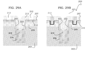
figures 26 (A-B) to 29(A-B) show the schematic, section views of a power MOSFET device with a field plate structure during the successive steps of the manufacturing method, according to a second aspect of the invention; -
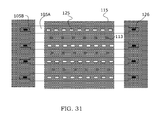
figures 30 and31 show schematic views from above of a first alternative embodiment of the geometry or layout of the gate and buried source contacts respectively for a single trench or for a plurality of trenches comprised into the MOSFET device being realised with the manufacturing method according to the invention; -
figure 32 shows the schematic view from above of a second alternative embodiment of the layout of the gate and buried source contacts for a plurality of trenches comprised into the MOSFET device being realised with the manufacturing method according to the invention; -
figure 33 shows the schematic view from above of a third alternative embodiment of the layout of the gate and buried source contacts for a plurality of trenches comprised into the MOSFET device being realised with the manufacturing method according to the invention; -
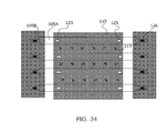
figure 34 shows the schematic view from above of a fourth alternative embodiment of the layout of the gate and buried source contacts for a plurality of trenches comprised into the MOSFET device being realised with the manufacturing method according to the invention; -
figure 35 shows the schematic view from above of a fifth alternative embodiment of the layout of the gate and buried source contacts for a plurality of trenches comprised into the MOSFET device being realised with the manufacturing method according to the invention; -
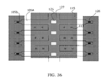
figure 36 shows the schematic view from above of a sixth alternative embodiment of the layout of the gate and buried source contacts for a plurality of trenches comprised into the MOSFET device being realised with the manufacturing method according to the invention; -
figure 37 shows the schematic view from above of a seventh alternative embodiment of the layout of the gate and buried source contacts for a plurality of trenches comprised into the MOSFET device being realised with the manufacturing method according to the invention; -
figure 38 shows the schematic view form above of an eighth alternative embodiment of the layout of the gate and buried source contacts for a plurality of trenches comprised into the MOSFET device being realised with the manufacturing method according to the invention. - With reference to these figures, the method for manufacturing a power device integrated on a semiconductor substrate and comprising a vertical and three-dimension field plate structure is now described in detail. In particular, the manufacturing method of the present invention allows to realise a power MOSFET device with a field plate structure by using a single deposition of polysilicon layer for the simultaneous formation of the gate electrode and of the buried source electrode.
- Moreover, the figures showing schematic views of portions of integrated devices during the manufacturing steps are not drawn to scale, but they are described in such a way as to highlight the important features of the invention.
- The present invention has the aim of optimizing the manufacturing method and the electric characteristics of a power device, in particular based on a vertical field plate structure, using a simpler and less expensive method with respect to the known solutions.
- As it will be clarified by the following description, the method according to an embodiment the invention combines conventional steps and innovative steps for realising a single polysilicon deposition for the formation of the gate and buried source electrodes. Advantageously according to the invention, a deep trench is realised having a narrowing in its end portions.
- In particular, with reference to
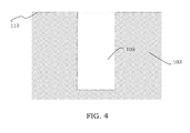
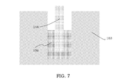
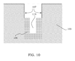
Figures 3 to 11 , a conventional method for manufacturing aMOSFET device 100 with the field plate technique comprises the known steps of: - growth on a silicon substrate, not shown in the figures, of an epitaxial layer or
silicon bulk 103; - conventional photo-lithography of the epitaxial layer, as shown in
figure 3 , through a first deposition of ahard mask layer 116 of dielectric material, deposition of a resist film, not shown in the figure, on the whole surface of thehard mask layer 116; masking through a photo-lithographic mask; UV exposure of the resist film in the areas not covered by the mask; development of the resist film in exposed areas; etching through the window defined by the photo-exposed resist film; removal of the resist film; etching of theepitaxial layer 103 for the formation of adeep trench 105 through the window defined by thehard mask layer 116; - removal of the
hard mask layer 116; growth of asacrificial layer 117 of dielectric material, for example silicon oxide, useful for compensating the damages caused by the etching step to the surface of theepitaxial layer 103, as shown infigure 4 ; - deposition of a
dielectric layer 106, in particular of thick oxide, for example TEOS, of thickness F suitably chosen according to the class of voltage of the device MOS and that partially fills in thetrench 105, as shown infigure 5 ; - filling of the
trench 105 with a layer of sacrificial material, 118, for example resist or bark, silicon nitride or polysilicon and planarization of the surface of theepitaxial layer 103, as shown infigure 6 ; - controlled wet etching of the
dielectric layer 106 with consequent retrocession below the surface of theepitaxial layer 103 of a distance comprised between approximately 1µm and 2µm, as shown infigure 7 ; - selective etching of the layer of
sacrificial material 118 with consequent formation of anempty region 119 within the trench, as shown infigure 8 and9 ; - growth of a layer of
gate oxide 107, as shown infigures 10 and11 . - For executing the selective etching of the layer of
sacrificial material 118, the material used for this layer is different with respect to the material used for thedielectric layer 106. In particular, if for thedielectric layer 106 silicon oxide is used, the layer ofsacrificial material 118 may be resist, bark (a material similar to the resist but much more conformal), silicon nitride or polysilicon. - Moreover, advantageously according to an embodiment of the invention, phototechnique is not necessary for removing the layer of
sacrificial material 118. In fact an immersion wet etching is used being specific for the sacrificial material of thislayer 118. In particular, by using resist, bark, nitride or polysilicon for this layer ofsacrificial material 118, the selectivity is so high, with respect to the e.g. silicon oxide that realises thedielectric layer 106, that an additional photomasking may be saved. - As it appears evident from
figure 9 , thetrench 105 has a narrowing in its end part and, in particular, it comprises anenlarged portion 105A of width D1 and anarrow portion 105B of width D2 being smaller than D1. These portions, in the junction region, have walls oriented at an angle α comprised between approximately 10° and 90°. - With particular reference to the examples of
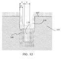
figures 12 to 25 , the method according to the invention goes on with a deposition step of a conductive filling layer, inparticular polysilicon 120 on the surface of theepitaxial layer 103, on the vertical walls of thetrench 105 and within theregion 119. P indicates the maximum value of the thickness of thispolysilicon layer 120 on the vertical walls of thetrench 105 and T indicates a process value equal to the difference between the width D1 of theenlarged portion 105A and twice the thickness of thedielectric layer 106, in particular thick oxide (T=D1-2F), i.e. the width of the trench minus the two lateral layers, as shown infigure 12 . Both these values may be chosen during the design step according to the class of voltage. To fill in with thepolysilicon layer 120 the whole width T of the cavity it is enough that P is greater than or equal to half T (P≥T/2). - The width D2 of the
portion 105B of thetrench 105 is smaller or equal to double the value F of the thickness of thedielectric layer 106, in particular thick oxide, (D2 ≦ 2F). In this way, thetrench 105B of width D2 may completely filled in by thedielectric layer 106, without cavity inside, as shown for example infigure 9 . - In substance, in the design of the
MOSFET device 100 the following rules are to be taken into consideration: - (T/2) ≦ P ≦ F; and
- D2 ≦ 2F
- Therefore, as shown in
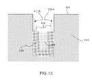
figure 13 , the method according to an aspect of the invention goes on with the execution of a dry anisotropic etching step of thepolysilicon layer 120, which determines the formation of a first and of asecond spacer front portion 105A of thetrench 105 and ofspacers narrow portion 105B of thetrench 105, which, as effect of the narrowing of the trench in thisnarrow portion 105B, are joined together.Figure 14 also shows the three-dimension section of the structure shown infigure 13 wherein it is evident that, as effect of the narrowing of thetrench 105 in itsnarrow portion 105B, thespacers narrow portion 105B. - During the etching step of the polysilicon layer the buried
source region 104 and thegate region 108, shown infigure 13 and14 are simultaneously realised. - The successive step of the method according to the invention consists in the formation of a
thin oxide layer 123 on thespacers 121 and on the buriedsource region 104, as shown infigure 15 , obtained through thermal oxidation and having the aim of creating a further insulating layer between the gate electrode and the buried source electrode and oxidizing possible conductive bridges between thegate region 108 and the buriedsource region 104. - In one alternative embodiment of the method according to the invention, after the formation of the
spacers figure 16 , which comprises alayer 124 of metallic silicide, for example cobalt silicide (CoSi2) or titanium silicide (TiSi) or tungsten silicide (WSi). - The metallic silicide is useful to remarkably reduce the value Rg of the gate resistance of the device and, in consequence, to obtain high switch speed of the device and low losses in dissipation during the transients.
- The successive manufacturing steps of the device are known but they are described hereafter for completeness of description.
- In particular, the method comprises the steps of:
- implantation of a
body region 109 and of asource region 110, followed by a suitable diffusion for activating the implanted doping species and the formation of the channel region, as shown infigure 17 ; - deposition of a
dielectric layer 111, for example glass boron-phosphosilicate or BPSG, useful for sealing and insulate the structure from the successive step of source metallization; masking and etching for realising, in thebody 109 andsource 110 region, a trench or micro-trench 112 useful for defining the body and source contacts, as shown infigure 18 ; - sputtering of a barrier
metallic layer 113b, for example titanium silicide (TiSi2); deposition of acontact tungsten layer 113, or WPlug, for filling the micro-trench 112; planarization, as shown infigure 19 . - In consequence of the fact that the
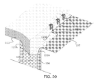
spacers narrow portion 105B of thetrench 105, it is possible to contact the gate region or electrode through gate contacts realised in thisnarrow portion 105B.Figure 20 shows the three-dimensional section of the structure offigure 19 comprisinggate contact regions 126 realised in thenarrow portion 105B of thetrench 105 and that serve as a contact with thepolysilicon layer 120 in electric continuity with thespacers - In particular, the tungsten layer simultaneously realises both the
contacts 113 on the active silicon are, and thecontacts 125 for the buried source of thepolysilicon layer 104. Subsequently, as it will be described hereafter, onemetallic layer 115 short-circuits theactive area contacts 113 with those realised on the buriedsource 125. Thebarrier layer 113b, in particular silicide, is realised under all the contacts, both ofactive area 113, and on the buriedsource 125, and on thegate 126. Thisbarrier layer 113b is shown for example inFigures 19 and25 , but it is not always indicated in all the other figures so as not to burden their representations. - A drain contact is instead realised with a metallization on the rear of the slice, this metallization being independent from the one used for creating the source electrode, with a process being shared by all the vertical PowerMOSFET devices independently from the technology and neither described nor shown in the figures.
- The method goes on with the process steps useful to realise the contacts for the buried
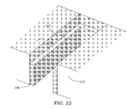
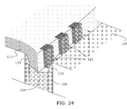
source electrode 104. Without depriving the generality of the description of anything and for sake of figure simplicity, the description of these steps is made considering atrench 105 that does not show a narrowing in the end portion. In this case, with the method according to the invention, the structure shown in 3D view infigure 21 is realised, passing through the steps of: formation of the trench; growth of a sacrificial oxide layer; deposition of a dielectric layer; filling of the trench with a sacrificial layer; reduction of the dielectric layer through etching; removal of the sacrificial layer. -
Figures 22 ,23 and24 respectively show the 3D images of the structure formed further to the steps of: gate oxidation; deposition of the polysilicon layer for the formation of spacers; formation of thesource contacts 125 buried in thetrench 105. - The final step of the method, as shown in
figure 25 , consists in the deposition of ametallic layer 115, for example an alloy of aluminium-silicon-copper (AlSiCu) or of aluminium-copper (AlCu), for the formation of the source electrode and of the gate one (not shown in the figure). - In a second aspect of the method according to another embodiment of the invention, the method comprises the conventional steps of:
- subjecting an
epitaxial layer 203 to a first conventional photo-lithographic step for the formation of adeep trench 205; - deposition of a
dielectric layer 206, in particular thick oxide, for example TEOS, of thickness F; filling of thetrench 205 with a layer ofsacrificial material 218, for example resist or bark, silicon nitride or polysilicon; a planarization step of the surface of theepitaxial layer 203; a controlled wet etching of thedielectric layer 206, with retrocession below the surface of theepitaxial layer 203, as shown infigure 26A ; - implantation of the
body region 209 and of thesource region 210, as shown infigure 26B ; - removal of the layer of
sacrificial material 218 and formation of anempty region 219 within the layer ofsacrificial material 218 and growth of a layer ofgate oxide 207, as shown infigures 27A and 27B . - The method, according to the invention, goes on with the successive steps of:
- deposition of a conductive filling layer, in particular a
metallic layer 227, for example tungsten (W-plug), and formation of afirst spacer 221 and asecond tungsten spacer 222 that serve as ametallic gate electrode 208, further to etching of themetallic layer 227, as shown infigures 28A and 28B ; the metallic buriedsource region 204 is thus formed; - deposition of an
insulation dielectric layer 211 and realisation of theopenings 212 for the contacts, as shown infigure 29A ; - digging of the silicon for contacting the buried
body region 209 under thesource region 210 and filling of theopenings 212 with a metallic layer (for example tungsten) 213 and deposition of a final metallization layer 215, as shown infigure 29B . - The
device 200 thus obtained and shown infigure 29B , comprising both the metallic gate and buried source electrodes, turns out to be faster than a polysilicon gate device of at least one order of magnitude during the transients. As already indicated, the value Rg of the gate resistance of the device varies according to the material used for realising the gate itself. In particular, it is possible to obtain for gates having area equal to 3,2mm2, the following values of Rg and Rg/mm2:Rg Rg/mm2 Gate only of polysilicon 8 2,5 Hybrid gate (polysilicon+silicide) 3,8 1,1875 Only metallic gate 0,5 0,15625 -
Figures 30-38 show the view from above of a single strip oftrenches 105 comprised into the MOSFET device, obtained with the method according to the invention, comprising the gate and buried source contacts being realised with the method according to the invention but according to different alternative embodiments of the layout geometries. - In particular,
figure 30 shows a view from above of thetrench 105 comprising a first and a secondnarrow portion 105B and anenlarged portion 105A, also with an enlarged view (Zoom) of the gate contact portion 126 (Gate metal). According to a first geometry, in theportions 105B thegate contact 126 is realised, while in theportion 105A the buriedsource contacts 125 are positioned. -
Figure 31 shows a view from above of a plurality of strips oftrenches 105 with narrowing having a close layout of the buriedsource contacts 125 according to the embodiment shown infigure 30 . In this case the distance between a contact and the successive one can be compared to the same dimension of the contact. -
Figure 32 shows a view from above of a plurality of strips oftrenches 105 with narrowing having a spaced layout of the buriedsource contacts 125, according to a second geometry of the contacts. In this case the distance between a contact and the successive one is at least approximately 10 times greater than the dimension of the contact. -
Figure 33 shows a view from above of a plurality of strips oftrenches 105 with narrowing having a single buried source contact 125 positioned in the middle of theportion 105A of thetrench 105, according to a third geometry of the contacts. -
Figure 34 shows a view from above of a plurality of strips oftrenches 105 with narrowing having a first and a second buried source contact 125 positioned at the edge of theportion 105A of thetrench 105, according to a fourth geometry of the contacts. -
Figure 35 shows a view from above of a plurality of strips oftrenches 105 with narrowing having a single wide buriedcontact 125 positioned in the middle of theportion 105A of thetrench 105, according to a fifth geometry of the contacts. In this case the ratio between the greater dimension and the smaller one of the single wide buried contact is at least 10. -
Figure 36 shows a view from above of a plurality of strips oftrenches 105 with narrowing having a single wide buried source contact 125 positioned within asource finger 127 realised in the middle of theportion 105A of thetrench 105 and shared by all thetrenches 105, according to a sixth geometry of the contacts. -
Figure 37 shows a view from above of a plurality of strips oftrenches 105 with narrowing having a layout of the buriedsource contacts 125 according to one of the alternative embodiments shown infigures 31 to 36 and with a chain ofgate contacts 126 arranged on an edge shared by all thetrenches 105, according to a seventh geometry of the contacts. -
Figure 38 shows a view from above of an eighth geometry of contacts relative to a plurality of strips oftrenches 105 comprising anarrow portion 105B and anenlarged portion 105A, according to an alternative embodiment of the trench that has a narrowing only at one end, with an arrangement of the buriedsource contacts 125 according to one of the embodiments shown infigures 31 to 36 and with a chain ofgate contacts 126 arranged on an edge shared by all thetrenches 105 in correspondence with thenarrow portion 105B. - In conclusion, the method according to the embodiments of the invention allows, differently from the known solutions that use a double deposition and polysilicon masking, to execute a single polysilicon deposition step and a single dry anisotropic etching for simultaneously realise the gate and buried source electrodes of a power device with a field plate structure, through the use of an asymmetric trench structure comprising a narrowing in its end portion.
- Therefore, the method according to the embodiments of the invention allows to reduce the presence of faults one the wafer due to the reduction through successive steps and to reduce the manufacturing costs of the device.
- Another advantage of the described method consists in that the effects of the overlapping of parasite capacities between the gate and buried source electrodes are annulled.
- Furthermore, the method according to the embodiments of the invention allows to obtain a better control of the gate resistance Rg realising the gate electrode with metallic or metallic silicide spacer.
- Finally, a further advantage of the method described is that, by distributing the buried source contacts according to the configurations above described and shown in
figures 31 to 38 , a better control of the switching of the power device between the turn-on step and the switching-off step according to the applications required is obtained. - An embodiment of the above-described MOSFET Device may be part of a system (e.g. an automotive system), and the system may include an integrated circuit (e.g. a processor) coupled to the MOSFET Device. Furthermore, the MOSFET Device & Integrated circuit may be disposed on a same or on respective semiconductor dies.
- Obviously, a technician of the field, with the aim of meeting incidental and specific needs, will be allowed to introduce several modifications and variations to the above described method, all within the scope of protection of the invention as defined by the following claims.
Claims (14)
- Method for manufacturing a power device (100, 200) integrated on a semiconductor substrate comprising the steps of:- growth on said substrate of an epitaxial layer (103, 203);- photo-lithography and etching of said epitaxial layer (103, 203) for the formation of at least one deep trench (105, 205);- deposition of a dielectric layer (106, 206) with partial filling of said at least one trench (105, 205);- complete filling of said at least one trench (105, 205) with a layer of sacrificial material (118, 218);- selective etching of said dielectric layer (106, 206) with consequent retrocession below said layer of sacrificial material (118, 218);- selective etching of said layer of sacrificial material (118, 218) with consequent formation of an empty region (119) within said at least one trench (105, 205);- growth of a layer of gate oxide (107, 207);- formation of at least one gate region (108, 208), of at least one buried source region (104, 204), of at least one body region (109, 209) and of at least one source region (110, 210);- deposition of a dielectric layer (111, 211);- simultaneous formation of at least one gate contact (126), at least one body/source contact (113, 213) and at least one buried source contact (125);- formation of a source contact region (113) and of a gate contact region, through deposition, masking and etching of a metallization layer (115, 215);
characterised in that said step of formation of at least one gate region (108, 208) and of at least one buried source region (104, 204), electrically insulated, comprises the steps of:- executing a single deposition of a conductive filling material (120, 227) on said epitaxial layer (103, 203), on the vertical walls of said trench (105, 205) and within said empty region (119);- etching said conductive filling material (120, 227) forming a first spacer (121, 221) and a second spacer (122; 222), suitable for serving as a gate electrode (108, 208) and forming a buried source electrode (104, 204) within said empty region (119). - Method according to claim 1, characterised in that said formation step of at least one deep trench (105) comprises the formation of at least one enlarged portion (105A) and at least one narrow portion (105B).
- Method according to claim 2, characterised in that said formation of a first spacer (121, 221) and a second spacer (122; 222) comprises the formation of a first and a second spacer (121A, 122A) in said at least one enlarged portion (105A) and a first and a second spacer (121B, 122B) in said at least one narrow portion (105B).
- Method according to claim 2, characterised in that said first and second spacers (121B, 122B) are joined together in said at least one narrow portion (105B).
- Method according to claim 1, characterised in that said complete filling step of said at least one trench (105, 205) with a layer of sacrificial material (118, 218) uses a filling material different from a material deposited by said deposition step of a dielectric layer (106, 206).
- Method according to claim 5, characterised in that said deposition step of a dielectric layer (106, 206) deposits silicon oxide and said complete filling step of said at least one trench (105, 205) with a layer of sacrificial material (118, 218) uses a material chosen among resist, bark, silicon nitride and polysilicon.
- Power device (100, 200) integrated on a semiconductor substrate and comprising:- an epitaxial layer (103, 203);- at least one deep trench (105, 205) partially covered by a dielectric layer (106, 206) and comprising a buried source region (104, 204);- a gate oxide layer (107, 207);- at least one gate region (108, 208), at least one buried source region (104, 204), at least one body region (109, 209) and at least one source region (110, 210);- a dielectric layer (111, 211);- at least one gate contact (126) and at least one buried source contact (125);- at least one drain contact region and one source (110, 210) contact region (113);
said gate region (108, 208) comprising a first spacer (121, 221) and a second spacer (122, 222) being simultaneously realised to the formation of said buried source region (104, 204) and
said trench (105) comprises at least one enlarged portion (105A) of width D1 and at least one narrow portion (105B) of width D2 being smaller than D1, said enlarged (105A) and narrow (105B) portions having in the conjunction region walls oriented at an angle α comprised between approximately 10° and 90°
characterised in that said at least one narrow portion (105B) comprises a plurality of gate contacts (126) and said at least one enlarged portion (105A) comprises a plurality of buried source contacts (125). - Device according to claim 7, characterised in that said first spacer (121) and second spacer (122) respectively comprise a first and a second spacer (121A, 122A) in said at least one enlarged portion (105A) and a first and a second spacer (121B, 122B) in said at least one narrow portion (105B).
- Device according to claim 8, characterised in that said first and second spacers (121B, 122B) are joined in said at least one narrow portion (105B).
- Device according to claim 7, characterised in that the buried source contacts (125) of said plurality are very close to each other, the distance between a contact and the successive one being comparable to the dimension of a contact.
- Device according to claim 7, characterised in that said plurality of gate contacts (126) comprises a chain of gate contacts (126) arranged on the edge of said at least one trench (105).
- Device according to claim 7, characterised in that the buried source contacts (125) of said plurality are very far from each other, the distance between a contact and the successive one being at least 10 times bigger than the dimension of a contact.
- Device according to claim 7, characterised in that said plurality of buried source contacts (125) comprises a first and a second buried source contact (125) positioned at the edge of said portion (105A).
- Device according to any of claims 7 to 13, characterised in that said plurality of gate contacts (126) comprises a chain of gate contacts (126) arranged on the edge of said at least one trench (105), said trench comprising at least one enlarged portion (105A) and a single narrow portion (105B).
Applications Claiming Priority (1)
| Application Number | Priority Date | Filing Date | Title |
|---|---|---|---|
| ITMI20092314 | 2009-12-28 |
Publications (2)
| Publication Number | Publication Date |
|---|---|
| EP2339636A1 true EP2339636A1 (en) | 2011-06-29 |
| EP2339636B1 EP2339636B1 (en) | 2019-03-13 |
Family
ID=42651059
Family Applications (1)
| Application Number | Title | Priority Date | Filing Date |
|---|---|---|---|
| EP10196923.6A Not-in-force EP2339636B1 (en) | 2009-12-28 | 2010-12-23 | Power semiconductor device and manufacturing method |
Country Status (2)
| Country | Link |
|---|---|
| US (2) | US8558305B2 (en) |
| EP (1) | EP2339636B1 (en) |
Cited By (5)
| Publication number | Priority date | Publication date | Assignee | Title |
|---|---|---|---|---|
| CN103021828A (en) * | 2011-09-22 | 2013-04-03 | 英飞凌科技奥地利有限公司 | Method for producing an electrode structure |
| CN104051503A (en) * | 2013-03-15 | 2014-09-17 | 飞兆半导体公司 | Apparatus associated with a termination area of a semiconductor device |
| WO2015150023A1 (en) * | 2014-04-03 | 2015-10-08 | Robert Bosch Gmbh | Method for producing a dielectric magneto resistor in a substrate trench, a corresponding substrate, and a power transistor |
| EP3499550A4 (en) * | 2016-08-31 | 2020-04-01 | CSMC Technologies Fab2 Co., Ltd. | VDMOS DEVICE AND MANUFACTURING METHOD THEREOF |
| CN117558761A (en) * | 2024-01-10 | 2024-02-13 | 湖北九峰山实验室 | A wide bandgap semiconductor trench MOSFET device and its manufacturing method |
Families Citing this family (14)
| Publication number | Priority date | Publication date | Assignee | Title |
|---|---|---|---|---|
| US8558305B2 (en) | 2009-12-28 | 2013-10-15 | Stmicroelectronics S.R.L. | Method for manufacturing a power device being integrated on a semiconductor substrate, in particular having a field plate vertical structure and corresponding device |
| JP2013065774A (en) | 2011-09-20 | 2013-04-11 | Toshiba Corp | Semiconductor device and manufacturing method of the same |
| US20130164895A1 (en) * | 2011-12-12 | 2013-06-27 | Maxpower Semiconductor, Inc. | Trench-Gated Power Devices with Two Types of Trenches and Reliable Polycidation |
| KR20150011185A (en) | 2013-07-22 | 2015-01-30 | 삼성전자주식회사 | Semiconductor device and method for fabricating the same |
| US9449968B2 (en) * | 2013-12-27 | 2016-09-20 | Infineon Technologies Austria Ag | Method for manufacturing a semiconductor device and a semiconductor device |
| US9209305B1 (en) * | 2014-06-06 | 2015-12-08 | Stmicroelectronics, Inc. | Backside source-drain contact for integrated circuit transistor devices and method of making same |
| US9397008B1 (en) * | 2015-04-21 | 2016-07-19 | United Microelectronics Corp. | Semiconductor device and manufacturing method of conductive structure in semiconductor device |
| US10854759B2 (en) * | 2016-04-01 | 2020-12-01 | Diodes Incorporated | Trenched MOS gate controlled rectifier |
| CN107785426B (en) * | 2016-08-31 | 2020-01-31 | 无锡华润上华科技有限公司 | kinds of semiconductor devices and their manufacture |
| US10658486B2 (en) * | 2017-05-18 | 2020-05-19 | Taiwan Semiconductor Manufacutring Co., Ltd. | Mitigation of time dependent dielectric breakdown |
| CN109378344A (en) * | 2018-12-11 | 2019-02-22 | 张家港凯思半导体有限公司 | A kind of ultra-low power consumption semiconductor power device and preparation method thereof |
| DE102019101304B4 (en) * | 2019-01-18 | 2023-04-27 | Infineon Technologies Dresden GmbH & Co. KG | Power semiconductor device and method of forming a power semiconductor device |
| TWI706452B (en) * | 2019-04-11 | 2020-10-01 | 台灣茂矽電子股份有限公司 | Manufacturing method of gate structure and gate structure |
| CN113035701B (en) * | 2021-03-12 | 2024-05-07 | 重庆万国半导体科技有限公司 | A gate resistance adjustable super junction power device and manufacturing method thereof |
Citations (8)
| Publication number | Priority date | Publication date | Assignee | Title |
|---|---|---|---|---|
| US20040089910A1 (en) | 2002-03-19 | 2004-05-13 | Infineon Technologies Ag | Power transistor |
| US7005351B2 (en) | 2002-03-19 | 2006-02-28 | Infineon Technologies Ag | Method for fabricating a transistor configuration including trench transistor cells having a field electrode, trench transistor, and trench configuration |
| US7183610B2 (en) | 2004-04-30 | 2007-02-27 | Siliconix Incorporated | Super trench MOSFET including buried source electrode and method of fabricating the same |
| US20070296039A1 (en) | 2006-06-21 | 2007-12-27 | Dureseti Chidambarrao | Semiconductor Device Structures Incorporating Voids and Methods of Fabricating Such Structures |
| US7372103B2 (en) | 2005-03-31 | 2008-05-13 | Infineon Technologies Austria Ag | MOS field plate trench transistor device |
| US7482654B2 (en) | 2004-04-20 | 2009-01-27 | International Rectifier Corporation | MOSgated power semiconductor device with source field electrode |
| US7504303B2 (en) | 2005-05-26 | 2009-03-17 | Fairchild Semiconductor Corporation | Trench-gate field effect transistors and methods of forming the same |
| US20090152624A1 (en) * | 2007-12-17 | 2009-06-18 | Infineon Technologies Austria Ag | Integrated circuit device with a semiconductor body and method for the production of an integrated circuit device |
Family Cites Families (2)
| Publication number | Priority date | Publication date | Assignee | Title |
|---|---|---|---|---|
| DE102005009020B4 (en) * | 2005-02-28 | 2012-04-26 | Infineon Technologies Austria Ag | Method for generating a power transistor and thus generated integrated circuit arrangement |
| US8558305B2 (en) * | 2009-12-28 | 2013-10-15 | Stmicroelectronics S.R.L. | Method for manufacturing a power device being integrated on a semiconductor substrate, in particular having a field plate vertical structure and corresponding device |
-
2010
- 2010-12-21 US US12/974,778 patent/US8558305B2/en not_active Expired - Fee Related
- 2010-12-23 EP EP10196923.6A patent/EP2339636B1/en not_active Not-in-force
-
2013
- 2013-03-13 US US13/801,975 patent/US8860131B2/en active Active
Patent Citations (9)
| Publication number | Priority date | Publication date | Assignee | Title |
|---|---|---|---|---|
| US20040089910A1 (en) | 2002-03-19 | 2004-05-13 | Infineon Technologies Ag | Power transistor |
| US7005351B2 (en) | 2002-03-19 | 2006-02-28 | Infineon Technologies Ag | Method for fabricating a transistor configuration including trench transistor cells having a field electrode, trench transistor, and trench configuration |
| US7482654B2 (en) | 2004-04-20 | 2009-01-27 | International Rectifier Corporation | MOSgated power semiconductor device with source field electrode |
| US7183610B2 (en) | 2004-04-30 | 2007-02-27 | Siliconix Incorporated | Super trench MOSFET including buried source electrode and method of fabricating the same |
| US7557409B2 (en) | 2004-04-30 | 2009-07-07 | Siliconix Incorporated | Super trench MOSFET including buried source electrode |
| US7372103B2 (en) | 2005-03-31 | 2008-05-13 | Infineon Technologies Austria Ag | MOS field plate trench transistor device |
| US7504303B2 (en) | 2005-05-26 | 2009-03-17 | Fairchild Semiconductor Corporation | Trench-gate field effect transistors and methods of forming the same |
| US20070296039A1 (en) | 2006-06-21 | 2007-12-27 | Dureseti Chidambarrao | Semiconductor Device Structures Incorporating Voids and Methods of Fabricating Such Structures |
| US20090152624A1 (en) * | 2007-12-17 | 2009-06-18 | Infineon Technologies Austria Ag | Integrated circuit device with a semiconductor body and method for the production of an integrated circuit device |
Cited By (13)
| Publication number | Priority date | Publication date | Assignee | Title |
|---|---|---|---|---|
| CN103021828A (en) * | 2011-09-22 | 2013-04-03 | 英飞凌科技奥地利有限公司 | Method for producing an electrode structure |
| CN104051503A (en) * | 2013-03-15 | 2014-09-17 | 飞兆半导体公司 | Apparatus associated with a termination area of a semiconductor device |
| EP2779248A3 (en) * | 2013-03-15 | 2015-01-14 | Fairchild Semiconductor Corporation | Apparatus related to termination regions of a semiconductor device |
| US10749027B2 (en) | 2013-03-15 | 2020-08-18 | Fairchild Semiconductor Corporation | Methods and apparatus related to termination regions of a semiconductor device |
| US9496391B2 (en) | 2013-03-15 | 2016-11-15 | Fairchild Semiconductor Corporation | Termination region of a semiconductor device |
| US9972690B2 (en) | 2014-04-03 | 2018-05-15 | Robert Bosch Gmbh | Method for producing a dielectric field plate in a substrate trench, a corresponding substrate, and a power transistor |
| JP2017516298A (en) * | 2014-04-03 | 2017-06-15 | ローベルト ボツシユ ゲゼルシヤフト ミツト ベシユレンクテル ハフツングRobert Bosch Gmbh | Method for manufacturing a dielectric field plate in a trench of a substrate, corresponding substrate and power transistor comprising such a substrate |
| WO2015150023A1 (en) * | 2014-04-03 | 2015-10-08 | Robert Bosch Gmbh | Method for producing a dielectric magneto resistor in a substrate trench, a corresponding substrate, and a power transistor |
| EP3499550A4 (en) * | 2016-08-31 | 2020-04-01 | CSMC Technologies Fab2 Co., Ltd. | VDMOS DEVICE AND MANUFACTURING METHOD THEREOF |
| US10868145B2 (en) | 2016-08-31 | 2020-12-15 | Csmc Technologies Fab2 Co., Ltd. | VDMOS device and manufacturing method therefor |
| US11532726B2 (en) | 2016-08-31 | 2022-12-20 | Csmc Technologies Fab2 Co., Ltd. | VDMOS device and manufacturing method therefor |
| CN117558761A (en) * | 2024-01-10 | 2024-02-13 | 湖北九峰山实验室 | A wide bandgap semiconductor trench MOSFET device and its manufacturing method |
| CN117558761B (en) * | 2024-01-10 | 2024-04-05 | 湖北九峰山实验室 | A wide bandgap semiconductor trench MOSFET device and a manufacturing method thereof |
Also Published As
| Publication number | Publication date |
|---|---|
| US20110156140A1 (en) | 2011-06-30 |
| US8860131B2 (en) | 2014-10-14 |
| EP2339636B1 (en) | 2019-03-13 |
| US8558305B2 (en) | 2013-10-15 |
| US20130270630A1 (en) | 2013-10-17 |
Similar Documents
| Publication | Publication Date | Title |
|---|---|---|
| EP2339636B1 (en) | Power semiconductor device and manufacturing method | |
| US6987305B2 (en) | Integrated FET and schottky device | |
| US8394702B2 (en) | Method for making dual gate oxide trench MOSFET with channel stop using three or four masks process | |
| US8187939B2 (en) | Direct contact in trench with three-mask shield gate process | |
| US8637369B2 (en) | Method for manufacturing an integrated power device having gate structures within trenches | |
| US8907415B2 (en) | High switching trench MOSFET | |
| US7186618B2 (en) | Power transistor arrangement and method for fabricating it | |
| US9806175B2 (en) | Power MOSFET device structure for high frequency applications | |
| KR101729935B1 (en) | Method of forming an insulated gate field effect transistor device having a shield electrode structure | |
| CN101371343B (en) | Self-aligned trench MOSFET structure and fabrication method | |
| US20100264488A1 (en) | Low Qgd trench MOSFET integrated with schottky rectifier | |
| US20070004116A1 (en) | Trenched MOSFET termination with tungsten plug structures | |
| TWI528423B (en) | Methods for fabricating semiconductor device and semiconductor device | |
| CN107910269B (en) | Power semiconductor device and method of manufacturing the same | |
| CN107910266B (en) | Power semiconductor device and method of manufacturing the same | |
| CN107910268B (en) | Power semiconductor device and method of manufacturing the same | |
| US20250151321A1 (en) | Semiconductor device having a trench field electrode with a first section buried below a gate electrode a second section for contacting | |
| CN107910271B (en) | Power semiconductor device and manufacturing method thereof | |
| CN114823869A (en) | Field effect transistor and method of manufacturing field effect transistor | |
| US20250113534A1 (en) | Method for producing a transistor device and transistor device | |
| WO2013090401A1 (en) | Self-aligned gate structure for field effect transistor | |
| KR20220169927A (en) | Power semiconductor device having low-k dielectric gaps between adjacent metal contacts | |
| HK1144492B (en) | Semiconductor component and method of manufacture | |
| HK1144492A1 (en) | Semiconductor component and method of manufacture | |
| HK1112112B (en) | Semiconductor power device having a top-side drain using a sinker trench |
Legal Events
| Date | Code | Title | Description |
|---|---|---|---|
| PUAI | Public reference made under article 153(3) epc to a published international application that has entered the european phase |
Free format text: ORIGINAL CODE: 0009012 |
|
| AK | Designated contracting states |
Kind code of ref document: A1 Designated state(s): AL AT BE BG CH CY CZ DE DK EE ES FI FR GB GR HR HU IE IS IT LI LT LU LV MC MK MT NL NO PL PT RO RS SE SI SK SM TR |
|
| AX | Request for extension of the european patent |
Extension state: BA ME |
|
| 17P | Request for examination filed |
Effective date: 20111227 |
|
| RAP1 | Party data changed (applicant data changed or rights of an application transferred) |
Owner name: STMICROELECTRONICS SRL |
|
| 17Q | First examination report despatched |
Effective date: 20151218 |
|
| STAA | Information on the status of an ep patent application or granted ep patent |
Free format text: STATUS: EXAMINATION IS IN PROGRESS |
|
| GRAP | Despatch of communication of intention to grant a patent |
Free format text: ORIGINAL CODE: EPIDOSNIGR1 |
|
| STAA | Information on the status of an ep patent application or granted ep patent |
Free format text: STATUS: GRANT OF PATENT IS INTENDED |
|
| INTG | Intention to grant announced |
Effective date: 20181002 |
|
| RIN1 | Information on inventor provided before grant (corrected) |
Inventor name: ZARA, FABIO |
|
| GRAS | Grant fee paid |
Free format text: ORIGINAL CODE: EPIDOSNIGR3 |
|
| GRAA | (expected) grant |
Free format text: ORIGINAL CODE: 0009210 |
|
| STAA | Information on the status of an ep patent application or granted ep patent |
Free format text: STATUS: THE PATENT HAS BEEN GRANTED |
|
| AK | Designated contracting states |
Kind code of ref document: B1 Designated state(s): AL AT BE BG CH CY CZ DE DK EE ES FI FR GB GR HR HU IE IS IT LI LT LU LV MC MK MT NL NO PL PT RO RS SE SI SK SM TR |
|
| REG | Reference to a national code |
Ref country code: GB Ref legal event code: FG4D |
|
| REG | Reference to a national code |
Ref country code: CH Ref legal event code: EP Ref country code: AT Ref legal event code: REF Ref document number: 1108882 Country of ref document: AT Kind code of ref document: T Effective date: 20190315 |
|
| REG | Reference to a national code |
Ref country code: DE Ref legal event code: R096 Ref document number: 602010057506 Country of ref document: DE |
|
| REG | Reference to a national code |
Ref country code: IE Ref legal event code: FG4D |
|
| REG | Reference to a national code |
Ref country code: NL Ref legal event code: MP Effective date: 20190313 |
|
| REG | Reference to a national code |
Ref country code: LT Ref legal event code: MG4D |
|
| PG25 | Lapsed in a contracting state [announced via postgrant information from national office to epo] |
Ref country code: LT Free format text: LAPSE BECAUSE OF FAILURE TO SUBMIT A TRANSLATION OF THE DESCRIPTION OR TO PAY THE FEE WITHIN THE PRESCRIBED TIME-LIMIT Effective date: 20190313 Ref country code: SE Free format text: LAPSE BECAUSE OF FAILURE TO SUBMIT A TRANSLATION OF THE DESCRIPTION OR TO PAY THE FEE WITHIN THE PRESCRIBED TIME-LIMIT Effective date: 20190313 Ref country code: FI Free format text: LAPSE BECAUSE OF FAILURE TO SUBMIT A TRANSLATION OF THE DESCRIPTION OR TO PAY THE FEE WITHIN THE PRESCRIBED TIME-LIMIT Effective date: 20190313 Ref country code: NO Free format text: LAPSE BECAUSE OF FAILURE TO SUBMIT A TRANSLATION OF THE DESCRIPTION OR TO PAY THE FEE WITHIN THE PRESCRIBED TIME-LIMIT Effective date: 20190613 |
|
| PG25 | Lapsed in a contracting state [announced via postgrant information from national office to epo] |
Ref country code: RS Free format text: LAPSE BECAUSE OF FAILURE TO SUBMIT A TRANSLATION OF THE DESCRIPTION OR TO PAY THE FEE WITHIN THE PRESCRIBED TIME-LIMIT Effective date: 20190313 Ref country code: LV Free format text: LAPSE BECAUSE OF FAILURE TO SUBMIT A TRANSLATION OF THE DESCRIPTION OR TO PAY THE FEE WITHIN THE PRESCRIBED TIME-LIMIT Effective date: 20190313 Ref country code: GR Free format text: LAPSE BECAUSE OF FAILURE TO SUBMIT A TRANSLATION OF THE DESCRIPTION OR TO PAY THE FEE WITHIN THE PRESCRIBED TIME-LIMIT Effective date: 20190614 Ref country code: BG Free format text: LAPSE BECAUSE OF FAILURE TO SUBMIT A TRANSLATION OF THE DESCRIPTION OR TO PAY THE FEE WITHIN THE PRESCRIBED TIME-LIMIT Effective date: 20190613 Ref country code: HR Free format text: LAPSE BECAUSE OF FAILURE TO SUBMIT A TRANSLATION OF THE DESCRIPTION OR TO PAY THE FEE WITHIN THE PRESCRIBED TIME-LIMIT Effective date: 20190313 Ref country code: NL Free format text: LAPSE BECAUSE OF FAILURE TO SUBMIT A TRANSLATION OF THE DESCRIPTION OR TO PAY THE FEE WITHIN THE PRESCRIBED TIME-LIMIT Effective date: 20190313 |
|
| REG | Reference to a national code |
Ref country code: AT Ref legal event code: MK05 Ref document number: 1108882 Country of ref document: AT Kind code of ref document: T Effective date: 20190313 |
|
| PG25 | Lapsed in a contracting state [announced via postgrant information from national office to epo] |
Ref country code: ES Free format text: LAPSE BECAUSE OF FAILURE TO SUBMIT A TRANSLATION OF THE DESCRIPTION OR TO PAY THE FEE WITHIN THE PRESCRIBED TIME-LIMIT Effective date: 20190313 Ref country code: PT Free format text: LAPSE BECAUSE OF FAILURE TO SUBMIT A TRANSLATION OF THE DESCRIPTION OR TO PAY THE FEE WITHIN THE PRESCRIBED TIME-LIMIT Effective date: 20190713 Ref country code: AL Free format text: LAPSE BECAUSE OF FAILURE TO SUBMIT A TRANSLATION OF THE DESCRIPTION OR TO PAY THE FEE WITHIN THE PRESCRIBED TIME-LIMIT Effective date: 20190313 Ref country code: SK Free format text: LAPSE BECAUSE OF FAILURE TO SUBMIT A TRANSLATION OF THE DESCRIPTION OR TO PAY THE FEE WITHIN THE PRESCRIBED TIME-LIMIT Effective date: 20190313 Ref country code: CZ Free format text: LAPSE BECAUSE OF FAILURE TO SUBMIT A TRANSLATION OF THE DESCRIPTION OR TO PAY THE FEE WITHIN THE PRESCRIBED TIME-LIMIT Effective date: 20190313 Ref country code: RO Free format text: LAPSE BECAUSE OF FAILURE TO SUBMIT A TRANSLATION OF THE DESCRIPTION OR TO PAY THE FEE WITHIN THE PRESCRIBED TIME-LIMIT Effective date: 20190313 Ref country code: EE Free format text: LAPSE BECAUSE OF FAILURE TO SUBMIT A TRANSLATION OF THE DESCRIPTION OR TO PAY THE FEE WITHIN THE PRESCRIBED TIME-LIMIT Effective date: 20190313 Ref country code: IT Free format text: LAPSE BECAUSE OF FAILURE TO SUBMIT A TRANSLATION OF THE DESCRIPTION OR TO PAY THE FEE WITHIN THE PRESCRIBED TIME-LIMIT Effective date: 20190313 |
|
| PG25 | Lapsed in a contracting state [announced via postgrant information from national office to epo] |
Ref country code: SM Free format text: LAPSE BECAUSE OF FAILURE TO SUBMIT A TRANSLATION OF THE DESCRIPTION OR TO PAY THE FEE WITHIN THE PRESCRIBED TIME-LIMIT Effective date: 20190313 Ref country code: PL Free format text: LAPSE BECAUSE OF FAILURE TO SUBMIT A TRANSLATION OF THE DESCRIPTION OR TO PAY THE FEE WITHIN THE PRESCRIBED TIME-LIMIT Effective date: 20190313 |
|
| REG | Reference to a national code |
Ref country code: DE Ref legal event code: R097 Ref document number: 602010057506 Country of ref document: DE |
|
| PG25 | Lapsed in a contracting state [announced via postgrant information from national office to epo] |
Ref country code: IS Free format text: LAPSE BECAUSE OF FAILURE TO SUBMIT A TRANSLATION OF THE DESCRIPTION OR TO PAY THE FEE WITHIN THE PRESCRIBED TIME-LIMIT Effective date: 20190713 Ref country code: AT Free format text: LAPSE BECAUSE OF FAILURE TO SUBMIT A TRANSLATION OF THE DESCRIPTION OR TO PAY THE FEE WITHIN THE PRESCRIBED TIME-LIMIT Effective date: 20190313 |
|
| PLBE | No opposition filed within time limit |
Free format text: ORIGINAL CODE: 0009261 |
|
| STAA | Information on the status of an ep patent application or granted ep patent |
Free format text: STATUS: NO OPPOSITION FILED WITHIN TIME LIMIT |
|
| PG25 | Lapsed in a contracting state [announced via postgrant information from national office to epo] |
Ref country code: DK Free format text: LAPSE BECAUSE OF FAILURE TO SUBMIT A TRANSLATION OF THE DESCRIPTION OR TO PAY THE FEE WITHIN THE PRESCRIBED TIME-LIMIT Effective date: 20190313 |
|
| 26N | No opposition filed |
Effective date: 20191216 |
|
| PG25 | Lapsed in a contracting state [announced via postgrant information from national office to epo] |
Ref country code: SI Free format text: LAPSE BECAUSE OF FAILURE TO SUBMIT A TRANSLATION OF THE DESCRIPTION OR TO PAY THE FEE WITHIN THE PRESCRIBED TIME-LIMIT Effective date: 20190313 |
|
| PGFP | Annual fee paid to national office [announced via postgrant information from national office to epo] |
Ref country code: FR Payment date: 20191120 Year of fee payment: 10 |
|
| PG25 | Lapsed in a contracting state [announced via postgrant information from national office to epo] |
Ref country code: TR Free format text: LAPSE BECAUSE OF FAILURE TO SUBMIT A TRANSLATION OF THE DESCRIPTION OR TO PAY THE FEE WITHIN THE PRESCRIBED TIME-LIMIT Effective date: 20190313 |
|
| REG | Reference to a national code |
Ref country code: CH Ref legal event code: PL |
|
| REG | Reference to a national code |
Ref country code: BE Ref legal event code: MM Effective date: 20191231 |
|
| PG25 | Lapsed in a contracting state [announced via postgrant information from national office to epo] |
Ref country code: MC Free format text: LAPSE BECAUSE OF FAILURE TO SUBMIT A TRANSLATION OF THE DESCRIPTION OR TO PAY THE FEE WITHIN THE PRESCRIBED TIME-LIMIT Effective date: 20190313 |
|
| GBPC | Gb: european patent ceased through non-payment of renewal fee |
Effective date: 20191223 |
|
| PG25 | Lapsed in a contracting state [announced via postgrant information from national office to epo] |
Ref country code: LU Free format text: LAPSE BECAUSE OF NON-PAYMENT OF DUE FEES Effective date: 20191223 Ref country code: IE Free format text: LAPSE BECAUSE OF NON-PAYMENT OF DUE FEES Effective date: 20191223 Ref country code: GB Free format text: LAPSE BECAUSE OF NON-PAYMENT OF DUE FEES Effective date: 20191223 |
|
| PG25 | Lapsed in a contracting state [announced via postgrant information from national office to epo] |
Ref country code: CH Free format text: LAPSE BECAUSE OF NON-PAYMENT OF DUE FEES Effective date: 20191231 Ref country code: LI Free format text: LAPSE BECAUSE OF NON-PAYMENT OF DUE FEES Effective date: 20191231 Ref country code: BE Free format text: LAPSE BECAUSE OF NON-PAYMENT OF DUE FEES Effective date: 20191231 |
|
| PGFP | Annual fee paid to national office [announced via postgrant information from national office to epo] |
Ref country code: DE Payment date: 20201119 Year of fee payment: 11 |
|
| PG25 | Lapsed in a contracting state [announced via postgrant information from national office to epo] |
Ref country code: CY Free format text: LAPSE BECAUSE OF FAILURE TO SUBMIT A TRANSLATION OF THE DESCRIPTION OR TO PAY THE FEE WITHIN THE PRESCRIBED TIME-LIMIT Effective date: 20190313 |
|
| PG25 | Lapsed in a contracting state [announced via postgrant information from national office to epo] |
Ref country code: MT Free format text: LAPSE BECAUSE OF FAILURE TO SUBMIT A TRANSLATION OF THE DESCRIPTION OR TO PAY THE FEE WITHIN THE PRESCRIBED TIME-LIMIT Effective date: 20190313 Ref country code: HU Free format text: LAPSE BECAUSE OF FAILURE TO SUBMIT A TRANSLATION OF THE DESCRIPTION OR TO PAY THE FEE WITHIN THE PRESCRIBED TIME-LIMIT; INVALID AB INITIO Effective date: 20101223 |
|
| PG25 | Lapsed in a contracting state [announced via postgrant information from national office to epo] |
Ref country code: FR Free format text: LAPSE BECAUSE OF NON-PAYMENT OF DUE FEES Effective date: 20201231 |
|
| PG25 | Lapsed in a contracting state [announced via postgrant information from national office to epo] |
Ref country code: MK Free format text: LAPSE BECAUSE OF FAILURE TO SUBMIT A TRANSLATION OF THE DESCRIPTION OR TO PAY THE FEE WITHIN THE PRESCRIBED TIME-LIMIT Effective date: 20190313 |
|
| REG | Reference to a national code |
Ref country code: DE Ref legal event code: R119 Ref document number: 602010057506 Country of ref document: DE |
|
| PG25 | Lapsed in a contracting state [announced via postgrant information from national office to epo] |
Ref country code: DE Free format text: LAPSE BECAUSE OF NON-PAYMENT OF DUE FEES Effective date: 20220701 |