EP2337338A1 - Method and system for x-droop correction in solid state image sensor - Google Patents
Method and system for x-droop correction in solid state image sensor Download PDFInfo
- Publication number
- EP2337338A1 EP2337338A1 EP10191036A EP10191036A EP2337338A1 EP 2337338 A1 EP2337338 A1 EP 2337338A1 EP 10191036 A EP10191036 A EP 10191036A EP 10191036 A EP10191036 A EP 10191036A EP 2337338 A1 EP2337338 A1 EP 2337338A1
- Authority
- EP
- European Patent Office
- Prior art keywords
- line memory
- value
- pixel
- average
- fpn
- Prior art date
- Legal status (The legal status is an assumption and is not a legal conclusion. Google has not performed a legal analysis and makes no representation as to the accuracy of the status listed.)
- Ceased
Links
- 238000000034 method Methods 0.000 title claims abstract description 44
- 239000007787 solid Substances 0.000 title claims abstract description 9
- 238000012937 correction Methods 0.000 title abstract description 26
- 238000012935 Averaging Methods 0.000 claims description 12
- 238000012545 processing Methods 0.000 claims description 3
- 230000005855 radiation Effects 0.000 claims description 3
- 238000005096 rolling process Methods 0.000 claims description 3
- 238000004364 calculation method Methods 0.000 claims description 2
- 238000004590 computer program Methods 0.000 claims 3
- 238000004422 calculation algorithm Methods 0.000 claims 1
- 230000000694 effects Effects 0.000 abstract description 9
- 230000007246 mechanism Effects 0.000 abstract description 8
- 230000002123 temporal effect Effects 0.000 abstract description 6
- 230000009467 reduction Effects 0.000 abstract description 2
- 230000008569 process Effects 0.000 description 8
- 230000000875 corresponding effect Effects 0.000 description 5
- 238000012546 transfer Methods 0.000 description 5
- 230000009471 action Effects 0.000 description 4
- 238000010586 diagram Methods 0.000 description 4
- 230000008901 benefit Effects 0.000 description 3
- 230000004075 alteration Effects 0.000 description 2
- 238000013459 approach Methods 0.000 description 2
- 239000003990 capacitor Substances 0.000 description 2
- 238000012986 modification Methods 0.000 description 2
- 230000004048 modification Effects 0.000 description 2
- 230000000737 periodic effect Effects 0.000 description 2
- 239000004065 semiconductor Substances 0.000 description 2
- 230000001052 transient effect Effects 0.000 description 2
- 230000001133 acceleration Effects 0.000 description 1
- 230000002596 correlated effect Effects 0.000 description 1
- 238000013461 design Methods 0.000 description 1
- 230000006870 function Effects 0.000 description 1
- 230000010354 integration Effects 0.000 description 1
- 239000000463 material Substances 0.000 description 1
- 230000003287 optical effect Effects 0.000 description 1
- 230000003071 parasitic effect Effects 0.000 description 1
- 230000000704 physical effect Effects 0.000 description 1
- 238000005070 sampling Methods 0.000 description 1
- 230000003068 static effect Effects 0.000 description 1
- 238000006467 substitution reaction Methods 0.000 description 1
Images





Classifications
-
- H—ELECTRICITY
- H04—ELECTRIC COMMUNICATION TECHNIQUE
- H04N—PICTORIAL COMMUNICATION, e.g. TELEVISION
- H04N25/00—Circuitry of solid-state image sensors [SSIS]; Control thereof
-
- H—ELECTRICITY
- H04—ELECTRIC COMMUNICATION TECHNIQUE
- H04N—PICTORIAL COMMUNICATION, e.g. TELEVISION
- H04N25/00—Circuitry of solid-state image sensors [SSIS]; Control thereof
- H04N25/60—Noise processing, e.g. detecting, correcting, reducing or removing noise
- H04N25/67—Noise processing, e.g. detecting, correcting, reducing or removing noise applied to fixed-pattern noise, e.g. non-uniformity of response
- H04N25/671—Noise processing, e.g. detecting, correcting, reducing or removing noise applied to fixed-pattern noise, e.g. non-uniformity of response for non-uniformity detection or correction
- H04N25/677—Noise processing, e.g. detecting, correcting, reducing or removing noise applied to fixed-pattern noise, e.g. non-uniformity of response for non-uniformity detection or correction for reducing the column or line fixed pattern noise
Definitions
- the present disclosure relates to solid state image sensors using CMOS technology, more particularly to method and system for correcting x-droop noise in solid state image sensors.
- Solid state image sensors normally include an array of pixels arranged in rows and columns which form a bi-dimensional image representation. An image is read out, row by row, via an array of Analogue to Digital Converters (ADC). Every pixel in a column of data is read out by the same ADC. As a result of process mismatch, the pixel data read out from a single column may have an associated offset with respect to its neighbours. Since this fixed offset will be apparent in every pixel read out by that ADC, i.e. a column of data, the resulting image artifact is commonly known as Vertical Fixed Pattern Noise (VFPN) or Fixed Pattern Noise (FPN).
- VFPN Vertical Fixed Pattern Noise
- FPN Fixed Pattern Noise
- US Patent Application 2005/0104981 discloses a method for correcting column FPN in image sensors which include an output circuit for each column for reading pixel image signals by means of a pair of sample capacitors and a switching circuit operable based upon pixel switches for applying pixel voltages to the pair of sample capacitors.
- Each column has an optically masked pixel which does not contribute to the image but is used to estimate the column FPN.
- An image processing circuit records the column FPN for each column from the optically masked pixels, records the image signal from the sensor array of active pixels and subtracts the column FPN column-wise from the image signal
- a method for limiting the x-droop effect in the digital image captured with solid state image sensors with a correction mechanism which instead of using only correction values from the same column to which the correction is applied, also takes the neighbouring pixels into account to provide an averaged value to aid in the reduction of temporal and fixed noise contributions associated with the readout of a single pixel.
- the method according to the present disclosure uses the average of a large number of samples to reduce the temporal noise contribution stored from the readout of information from the shielded pixels.
- the samples in this average are taken both in time, and across a number of columns in the x direction. These samples are then subtracted from the visible rows read out in an effort to cancel the droop visible in the final image.
- the present disclosure offers a number of benefits.
- One of the advantages of the method according to a preferred embodiment of the present disclosure is that the x-droop effect is counteracted with a simple correction mechanism which limits the total number of line readings required.
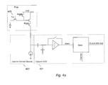
- each column of the pixel array shares a common ADC, termed 'Column ADC' 401 and column current source 403.
- the column current source and comparator biasing networks are laid out in repeating blocks across multiple columns as shown in Figure 4b .
- Bayer Scaling switches across several columns as this is a key requirement of their operation.
- Laying out the device in this manner is efficient, but it also opens up possibilities for periodic offset patterns in ADC output code values. This may be due to parasitic capacitances or resistances, or physical effects of column to column differences on transistor parameters.
- This periodic noise could be corrected with a Repeating FPN Correction mechanism as the one disclosed in co-pending application, filed on the same date by the same applicant and having the same inventor, with the title "Method and system for repeated fixed pattern noise correction".
- a line memory 501 is used to contain average dark samples of the M columns of array of active pixels 201.
- line memory 501 has the same size M as the rows of the array of active pixels (M is of course also the number of columns in the array 201); however other implementations are possible with the size of the line memory 501 being greater or smaller than the rows of the array of active pixels.
- Multiple reads of the optically masked line, or of several optically masked lines, are made and the results are digitally averaged into a line memory. It is worth noting that it may not be necessary to transfer charge from the photodiode itself when reading from the optically masked lines.
- each position in second line memory 503 will contain an average value based on the corresponding value of first line memory 501 and a number of neighbours positions.
- the number of neighbours used for calculating the average can vary according to several factors and it could be tuned also according to experimental results. In a preferred embodiment of the present disclosure such number is related to (e.g. a multiple of) the number of common readout repeating blocks across multiple columns mentioned above. The implementation of this averaging action can be done with several different techniques.
- Figure 6 shows two examples of averaging technique.
- the averaging operation in the x direction could be applied using a 'rolling average' methodology. This average would be applied over a width n, as illustrated in Figure 6 so that the 1 st to n-th locations of memory M are averaged and stored in location n/2 of a new memory P. The 2 nd to the (n+1)-th locations of memory M would then be averaged and stored in location (1+ n/2). This process would be repeated across the full array of memory M.
- the content of memory 503 is then provided to a Correction module 505 and used to correct the image signals being received from the active pixel array 201. For each visible pixel value read out the x-Droop correction data contained in memory 503 is subtracted.
- Figure 7 schematically shows a diagram representing the method steps of a preferred embodiment of the present disclosure.
- the process starts at circle 701 and it is transferred to box 703 where optically masked pixels from the dark area are read and averaged.
- the dark pixel area could include one single row of optically masked pixels or a plurality of rows.
- an averaging action is required. This activity could be done either by averaging the plurality of corresponding pixels in one position, or alternatively a plurality of reading of the same pixel to be sure the result is not affected by a temporary voltage problem or other contingent factors (this second averaging can be applied to the case where only one single row of dark pixel is available).
- Yet another option is to combine the two techniques above.
- the M-size line memory is then filled with the averaged value at box 705.
- the data of first line memory are used to generate the averaged value of second line memory which will be used to correct the x-droop noise of the read image.
- the way the average is calculated can vary according to specific requirement; in the same way the size of the range of neighbours used to calculate the average can be customised.
- such number N is related to the number of columns of common readout repeating blocks.
- An optional step is that of determining a global average factor (see box 709), calculated e.g. as a global average of all values of first M-sized line memory.
- Such Global Average factor can be added to corrected image signals so that the image mean is maintained.
- those values exceeding a given threshold T are not considered.
- the image signals can be read from the image sensor (see box 711) and processed by the correction mechanism.
- the image signals are corrected by subtracting the x-droop correction values and possibly adding the Global Average factor.
- the last two actions 711 and 713 in a preferred embodiment of the present disclosure are performed line by line and are repeated for each of the Y rows. The process can then restart with new samples taken from the optically masked area when e.g. a new frame of a moving image is received or a completely new image is to be processed.
- the program (which may be used to implement each embodiment of the disclosure) is structured in a different way, or if additional modules or functions are provided; likewise, the memory structures may be of other types, or may be replaced with equivalent entities (not necessarily consisting of physical storage media). Moreover, the proposed solution lends itself to be implemented with an equivalent method (having similar or additional steps, even in a different order).
- the program may take any form suitable to be used by or in connection with any data processing system, such as external or resident software, firmware, or microcode (either in object code or in source code).
- the program may be provided on any computer-usable medium; the medium can be any element suitable to contain, store, communicate, propagate, or transfer the program.
- Examples of such medium are fixed disks (where the program can be pre-loaded), removable disks, tapes, cards, wires, fibres, wireless connections, networks, broadcast waves, and the like; for example, the medium may be of the electronic, magnetic, optical, electromagnetic, infrared, or semiconductor type.
- the solution according to the present disclosure lends itself to be carried out with a hardware structure (for example, integrated in a chip of semiconductor material), or with a combination of software and hardware.
Landscapes
- Engineering & Computer Science (AREA)
- Multimedia (AREA)
- Signal Processing (AREA)
- Transforming Light Signals Into Electric Signals (AREA)
Abstract
According to one aspect of the present disclosure there is provided a method for limiting the x-droop effect in the digital image captured with solid state image sensors with a correction mechanism which instead of using only correction values from the same column to which the correction is applied, also takes the neighbouring pixels into account to provide an averaged value to aid in the reduction of temporal and fixed noise contributions associated with the readout of a single pixel.
Description
- The present disclosure relates to solid state image sensors using CMOS technology, more particularly to method and system for correcting x-droop noise in solid state image sensors.
- In state of the art digital image sensors a known problem is the so called x-droop noise which is normally due to differences in column ground plane voltage, process variation or transient signal effects across the horizontal direction (i.e. the "x direction" which gives the name to this effect).
- Solid state image sensors normally include an array of pixels arranged in rows and columns which form a bi-dimensional image representation. An image is read out, row by row, via an array of Analogue to Digital Converters (ADC). Every pixel in a column of data is read out by the same ADC. As a result of process mismatch, the pixel data read out from a single column may have an associated offset with respect to its neighbours. Since this fixed offset will be apparent in every pixel read out by that ADC, i.e. a column of data, the resulting image artifact is commonly known as Vertical Fixed Pattern Noise (VFPN) or Fixed Pattern Noise (FPN).
- One approach which has been used in the known systems to adjust the resulting image is to counteract the effect of FPN with a cancellation mechanism.
-
US Patent Application 2005/0104981 discloses a method for correcting column FPN in image sensors which include an output circuit for each column for reading pixel image signals by means of a pair of sample capacitors and a switching circuit operable based upon pixel switches for applying pixel voltages to the pair of sample capacitors. Each column has an optically masked pixel which does not contribute to the image but is used to estimate the column FPN. An image processing circuit records the column FPN for each column from the optically masked pixels, records the image signal from the sensor array of active pixels and subtracts the column FPN column-wise from the image signal - The technique discussed in
US Patent Application 2005/0104981 will remove from the correction data, for a sensor employing a Sample and Hold readout methodology, the temporal noise contribution of the pixel but it will not account for temporal noise associated with ADC circuitry. For a continuous time system, which performs an auto-zero operation on the black value and then maintains a continuous connection to the pixel to convert the signal component to a digital code, this methodology is not useful: there is no CDSSIG (Correlated Double Sampling SIGnal) pulse to remove. Removing the TG pulse will allow the reset noise contribution to be removed but noise from the source follower (dominated by Random Telegraphic Signal (RTS) noise and 1/f noise) in addition to other noise, including noise from the ADC, will remain. - With the approach described in
US Patent Application 2005/0104981 some noise contributions are stored in the correction data, including temporal noise from the comparator and kTC noise: these noise contributions will be added to pixels from the visible array and will introduce new Vertical Fixed Pattern noise components. Also the described is specific to a sample and hold readout methodology, and cannot be fully applied to a continuous time architecture. - It is an object of the present disclosure to overcome at least some of the problems associated with the prior art.
- The present disclosure provides a method and system as set out in the accompanying claims.
- According to one aspect of the present disclosure there is provided a method for limiting the x-droop effect in the digital image captured with solid state image sensors with a correction mechanism which instead of using only correction values from the same column to which the correction is applied, also takes the neighbouring pixels into account to provide an averaged value to aid in the reduction of temporal and fixed noise contributions associated with the readout of a single pixel.
- The method according to the present disclosure uses the average of a large number of samples to reduce the temporal noise contribution stored from the readout of information from the shielded pixels. The samples in this average are taken both in time, and across a number of columns in the x direction. These samples are then subtracted from the visible rows read out in an effort to cancel the droop visible in the final image.
- The present disclosure offers a number of benefits. One of the advantages of the method according to a preferred embodiment of the present disclosure is that the x-droop effect is counteracted with a simple correction mechanism which limits the total number of line readings required.
- Reference will now be made, by way of example, to the accompanying drawings, in which:
-
Figure 1 is a schematic representation of an example of x-droop noise; -
Figure 2 is a schematic diagram of an image sensor according to a preferred embodiment of the present disclosure; -
Figure 3 schematically shows the visible pixels and the optically masked pixels in the image sensor according to a preferred embodiment of the present disclosure; -
Figure 4a and4b schematically shows the circuit of an image sensor according to a preferred embodiment of the present disclosure; -
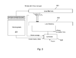
Figure 5 is a schematic diagram showing the method of averaging FPN correction pixels with a number of neighbours pixels according to a preferred embodiment of the present disclosure; -
Figure 6 shows an example of two different averaging techniques; -
Figure 7 is a diagram of the method steps of a preferred embodiment of the present disclosure. -
-
Figure 1 is a schematic representation of a possible x-droop noise effect in a solid state image sensor. Such noise is due to various factors, such for example differences in column ground plane voltage, process variation or transient signal effects across the horizontal direction. -
Figure 2 shows a CMOS integrated image sensor, according to a preferred embodiment of the present disclosure, having an array ofactive pixels 201 arranged inY rows 203 andM columns 205. To realize the correction mechanism, in a preferred embodiment of the present disclosure, the array ofactive pixels 201 includes at least one row of black (or dummy)pixels 207, which are identical to standard image pixels, but are not used to obtain image data. - These black pixels are optically masked, i.e. they are shielded from incident radiation, so that output image signals obtained from the optically masked pixels represent substantially only the related column FPN and can be used to correct such noise. Data from the dark pixels area are supplied to an
x-Droop Correction Mechanism 209 and are used to adjust the visible read out data obtained by thearray 201.Figure 3 shows the example of one column of visible pixels with the corresponding dark pixel which represents the column FPN and droop contribution and should be subtracted from each pixel of the same column. The dark pixel area can include a plurality of rows, e.g. according to a preferred embodiment of the present disclosure 24 physical rows of dark pixels will be addressed multiple times so that the total number of row reads is around 250. - For ease of description,
Figure 3 shows the simplified example of one column of visible pixels with the corresponding dark pixel which represents the column FPN and droop contribution which must be subtracted from each pixel of the same column. The array of active pixels of the system according to preferred embodiments of the present disclosure has been described in term of rows and - columns, just for ease of description. Those skilled in the art will easily appreciate that the terms rows and columns just want to indicate the two dimensions of the array of active pixels, but could of course be arranged in an inverse order so that the rows are columns and vice versa.
- As shown in
Figure 4a , in a preferred embodiment of the present disclosure each column of the pixel array shares a common ADC, termed 'Column ADC' 401 and columncurrent source 403. In order to optimise the layout of these components in terms of area and current consumption the column current source and comparator biasing networks are laid out in repeating blocks across multiple columns as shown inFigure 4b . Bayer Scaling switches across several columns as this is a key requirement of their operation. Laying out the device in this manner is efficient, but it also opens up possibilities for periodic offset patterns in ADC output code values. This may be due to parasitic capacitances or resistances, or physical effects of column to column differences on transistor parameters. This periodic noise could be corrected with a Repeating FPN Correction mechanism as the one disclosed in co-pending application, filed on the same date by the same applicant and having the same inventor, with the title "Method and system for repeated fixed pattern noise correction". - According to a preferred embodiment of the present disclosure a
line memory 501, as represented inFigure 5 is used to contain average dark samples of the M columns of array ofactive pixels 201. In the present example,line memory 501 has the same size M as the rows of the array of active pixels (M is of course also the number of columns in the array 201); however other implementations are possible with the size of theline memory 501 being greater or smaller than the rows of the array of active pixels. Multiple reads of the optically masked line, or of several optically masked lines, are made and the results are digitally averaged into a line memory. It is worth noting that it may not be necessary to transfer charge from the photodiode itself when reading from the optically masked lines. This means there may be no requirement to pulse the Transfer Gate (TG) (see 405 inFigure 4a ). Employing this technique will remove some noise contributions from the values read out, including reset noise. It also removes the requirement for an integration period, allowing acceleration of the readout if only one optically masked row is used. The preferred embodiment includes flexibility to assess the benefits of photodiode transfer against having no photodiode transfer, since its omission may compromise droop correction information relating to signal timings, or voltage drops across the pixel array. - The averaged line memory samples are then processed according to a preferred embodiment of the present disclosure so that, for each pixel correction represented in the first M-
size line memory 501 an adjusted value is calculated and copied to a second M-size line memory 503: according to a preferred embodiment of the present disclosure, each position insecond line memory 503 will contain an average value based on the corresponding value offirst line memory 501 and a number of neighbours positions. The number of neighbours used for calculating the average can vary according to several factors and it could be tuned also according to experimental results. In a preferred embodiment of the present disclosure such number is related to (e.g. a multiple of) the number of common readout repeating blocks across multiple columns mentioned above. The implementation of this averaging action can be done with several different techniques.Figure 6 shows two examples of averaging technique. The averaging operation in the x direction could be applied using a 'rolling average' methodology. This average would be applied over a width n, as illustrated inFigure 6 so that the 1st to n-th locations of memory M are averaged and stored in location n/2 of a new memory P. The 2nd to the (n+1)-th locations of memory M would then be averaged and stored in location (1+ n/2). This process would be repeated across the full array of memory M. There are numerous ways to generate samples for locations 1 to (n/2 - 1), i.e. beginning of the array, and for locations (M+1-n/2) to M, i.e. end of the array. Two options are: the use of a larger array so that M=P+n, or simply applying the same correction factor to locations 1 to (n/2 - 1) as is applied to location n/2 (same process should be applied to the last (n/2 -1) positions). Clearly further options could involve compromises between the two options mentioned here. It is also worth noting that, since the number of memory locations is an integer, and n is likely to be an even number, it may be necessary to apply the average of terms 1 to n to term (n/2 +/-) for this methodology to be functional. This rolling average gives a full line memory of data which is then used to correct the visible data read out on a column by column basis. - A static average is probably the simplest way to apply the average. Average samples 1 to n of M and store in location 1 of a memory Q, of width=M/n. Then average samples n+1 to 2n and store in location 2 of Q. Samples 2n+1 to 3n are averaged in location 3 of Q, and so on. When visible data is read out, location 1 of Q will be used to correct columns 1 to n. Location 2 will be used to correct columns n+1 to 2n, and so on. If M is not a multiple of n, then the final correction width (equal to n elsewhere) will be equal to n plus the remainder of M/n.
- This averaging process reduces the x-droop noise contribution in the correction data. The content of
memory 503 is then provided to aCorrection module 505 and used to correct the image signals being received from theactive pixel array 201. For each visible pixel value read out the x-Droop correction data contained inmemory 503 is subtracted. - As an optional additional feature, in order to improve the resulting image and in order to maintain the image mean while subtracting the x-droop correction data, it is advisable to add a value which is an average of all the averaged line memory samples. For each visible pixel value read out, this value is added, while the x-droop correction data is subtracted as explained above.
-
Figure 7 schematically shows a diagram representing the method steps of a preferred embodiment of the present disclosure. The process starts atcircle 701 and it is transferred tobox 703 where optically masked pixels from the dark area are read and averaged. As mentioned above the dark pixel area could include one single row of optically masked pixels or a plurality of rows. In case they are several, as in the preferred embodiment, an averaging action is required. This activity could be done either by averaging the plurality of corresponding pixels in one position, or alternatively a plurality of reading of the same pixel to be sure the result is not affected by a temporary voltage problem or other contingent factors (this second averaging can be applied to the case where only one single row of dark pixel is available). Yet another option is to combine the two techniques above. The M-size line memory is then filled with the averaged value atbox 705. Moving tobox 707 the data of first line memory are used to generate the averaged value of second line memory which will be used to correct the x-droop noise of the read image. According to a preferred embodiment, an averaging action is performed, so that, for each position mx (where 1 <= x <= M) in the first M-sized line memory, an average value according to the value of mx and the value of N neighbours positions in the first line memory is calculated and assigned to a corresponding position ml x in the second M-sized line memory. As explained above the way the average is calculated can vary according to specific requirement; in the same way the size of the range of neighbours used to calculate the average can be customised. In a preferred embodiment of the present disclosure such number N is related to the number of columns of common readout repeating blocks. An optional step is that of determining a global average factor (see box 709), calculated e.g. as a global average of all values of first M-sized line memory. Such Global Average factor can be added to corrected image signals so that the image mean is maintained. In a preferred embodiment of the present disclosure, in the calculation of such Global Average factor, those values exceeding a given threshold T are not considered. The image signals can be read from the image sensor (see box 711) and processed by the correction mechanism. Finally, atbox 713 the image signals are corrected by subtracting the x-droop correction values and possibly adding the Global Average factor. The last twoactions - It will be appreciated that alterations and modifications may be made to the above without departing from the scope of the disclosure. Naturally, in order to satisfy local and specific requirements, a person skilled in the art may apply to the solution described above many modifications and alterations. Particularly, although the present disclosure has been described with a certain degree of particularity with reference to preferred embodiment(s) thereof, it should be understood that various omissions, substitutions and changes in the form and details as well as other embodiments are possible; moreover, it is expressly intended that specific elements and/or method steps described in connection with any disclosed embodiment of the disclosure may be incorporated in any other embodiment as a general matter of design choice.
- Similar considerations apply if the program (which may be used to implement each embodiment of the disclosure) is structured in a different way, or if additional modules or functions are provided; likewise, the memory structures may be of other types, or may be replaced with equivalent entities (not necessarily consisting of physical storage media). Moreover, the proposed solution lends itself to be implemented with an equivalent method (having similar or additional steps, even in a different order). In any case, the program may take any form suitable to be used by or in connection with any data processing system, such as external or resident software, firmware, or microcode (either in object code or in source code). Moreover, the program may be provided on any computer-usable medium; the medium can be any element suitable to contain, store, communicate, propagate, or transfer the program. Examples of such medium are fixed disks (where the program can be pre-loaded), removable disks, tapes, cards, wires, fibres, wireless connections, networks, broadcast waves, and the like; for example, the medium may be of the electronic, magnetic, optical, electromagnetic, infrared, or semiconductor type.
- In any case, the solution according to the present disclosure lends itself to be carried out with a hardware structure (for example, integrated in a chip of semiconductor material), or with a combination of software and hardware.
Claims (13)
- A method for correcting x-droop noise from a digitally encoded image, captured with an image sensor, comprising an array of active pixels arranged in rows and columns, at least one row comprising optically masked pixels which are shielded from incident radiation, so that the output image signals obtained from each optically masked pixel substantially represent Fixed Pattern Noise (FPN) of the corresponding column, the method comprising:- recording into a first M-size line memory a value indicative of the FPN values of the optically masked pixels;- for each position mx (where 1 <= x <= M) in the first M-sized line memory calculating an average value according to the value of mx and the value of N neighbour positions in the first line memory and assigning to a corresponding position ml x in the second M-sized line memory a value indicative of the calculated average value;- reading the pixel image signals from the array of active pixels;- adjusting the read pixel image signals according to the content of the second M-size line memory.
- The method of claim 1 wherein the columns of array of active pixels are grouped in subsets of G columns having common blocks readout for reading the pixel image signals and wherein the number N of neighbouring pixel values used for averaging the value of each position mx of first line memory is integer multiple of G.
- The method of any preceding claim wherein adjusting the read pixel image signals includes:- subtracting the averaged values of second line memory from read pixel image signals.
- The method of any preceding claim wherein calculating an average value according to the value of mx and the value of N neighbours positions includes calculating the average using a rolling average algorithm.
- The method of any preceding claim wherein the value indicative of a column FPN recorded into the M-size line memory includes an average of all FPN values of the corresponding column of the at least one row of optically masked pixels.
- The method of any preceding claim wherein the value indicative of a column FPN recorded into the M-size line memory includes an average of multiple readings of the same FPN value of one optically masked pixel.
- The method of any preceding claim wherein adjusting the read pixel image signals includes:- adding to each pixel a global average factor calculated by averaging the values of the first M-size line memory.
- The method of claim 7 further including:- responsive to one of the values indicative of the FPN in the first M-size line memory exceeding a threshold T, do not include such value in the calculation of the global average factor.
- System for correcting x-droop noise from a digitally encoded image captured with an image sensor, comprising an array of active pixels arranged in rows and columns, at least one row comprising optically masked pixels which are shielded from incident radiation, so that the output image signals obtained from each optically masked pixel substantially represent FPN of the corresponding column, wherein the system comprises one or more components adapted to perform the method of any preceding claim.
- A solid state image sensor including the system of claim 9.
- A digital image processing device using the solid state image sensor of claim 10.
- Computer program comprising instructions for carrying out the method of any claim 1 to 8 when said computer program is executed on a computer system.
- An image correction software product including computer program of claim 12.
Applications Claiming Priority (1)
| Application Number | Priority Date | Filing Date | Title |
|---|---|---|---|
| GBGB0920930.5A GB0920930D0 (en) | 2009-11-30 | 2009-11-30 | Method and system for x-droop correction in solid state image sensor |
Publications (1)
| Publication Number | Publication Date |
|---|---|
| EP2337338A1 true EP2337338A1 (en) | 2011-06-22 |
Family
ID=41572894
Family Applications (1)
| Application Number | Title | Priority Date | Filing Date |
|---|---|---|---|
| EP10191036A Ceased EP2337338A1 (en) | 2009-11-30 | 2010-11-12 | Method and system for x-droop correction in solid state image sensor |
Country Status (3)
| Country | Link |
|---|---|
| US (1) | US8462235B2 (en) |
| EP (1) | EP2337338A1 (en) |
| GB (1) | GB0920930D0 (en) |
Families Citing this family (3)
| Publication number | Priority date | Publication date | Assignee | Title |
|---|---|---|---|---|
| JP6418839B2 (en) * | 2014-08-04 | 2018-11-07 | キヤノン株式会社 | Imaging apparatus, control method therefor, program, and storage medium |
| JP6064097B2 (en) * | 2014-12-19 | 2017-01-18 | オリンパス株式会社 | Endoscope and endoscope system |
| CN116055902B (en) * | 2022-12-30 | 2024-11-22 | 深圳锐视智芯科技有限公司 | Image generation method, device, image sensor and storage medium |
Citations (6)
| Publication number | Priority date | Publication date | Assignee | Title |
|---|---|---|---|---|
| EP1475957A1 (en) * | 2003-05-08 | 2004-11-10 | STMicroelectronics Limited | Method and apparatus for removing column fixed pattern noise in solid state image sensors |
| US20040233305A1 (en) * | 2003-05-23 | 2004-11-25 | Nikon Corporation | Shading correction circuit of electronic camera |
| EP1615426A1 (en) * | 2004-07-07 | 2006-01-11 | Sony Corporation | Signal processing device and method |
| US20060232692A1 (en) * | 2005-04-14 | 2006-10-19 | Fuji Photo Film Co., Ltd. | Image pickup apparatus |
| US7304670B1 (en) * | 1997-03-28 | 2007-12-04 | Hand Held Products, Inc. | Method and apparatus for compensating for fixed pattern noise in an imaging system |
| WO2009017920A1 (en) * | 2007-07-31 | 2009-02-05 | Micron Technology, Inc. | Method, apparatus, and system providing multi-column shared readout for imagers |
Family Cites Families (12)
| Publication number | Priority date | Publication date | Assignee | Title |
|---|---|---|---|---|
| US7133073B1 (en) * | 1999-08-19 | 2006-11-07 | Dialog Imaging Systems Gmbh | Method and apparatus for color interpolation |
| US7218351B2 (en) * | 2002-04-05 | 2007-05-15 | Victor Company Of Japan, Limited | Image-sensing apparatus for compensating video signal of a plurality of channels |
| JP4331553B2 (en) * | 2003-09-17 | 2009-09-16 | オリンパス株式会社 | Imaging device |
| US7564489B1 (en) * | 2005-02-18 | 2009-07-21 | Crosstek Capital, LLC | Method for reducing row noise with dark pixel data |
| JP2007013292A (en) * | 2005-06-28 | 2007-01-18 | Olympus Corp | Imaging device |
| US7427735B2 (en) * | 2005-12-14 | 2008-09-23 | Micron Technology, Inc. | Method and apparatus for setting black level in an imager using both optically black and tied pixels |
| US7545418B2 (en) * | 2006-07-17 | 2009-06-09 | Jeffery Steven Beck | Image sensor device having improved noise suppression capability and a method for supressing noise in an image sensor device |
| JP2008113141A (en) * | 2006-10-30 | 2008-05-15 | Fujifilm Corp | Imaging apparatus and signal processing method |
| US7999866B2 (en) * | 2007-05-21 | 2011-08-16 | Canon Kabushiki Kaisha | Imaging apparatus and processing method thereof |
| JP4424753B2 (en) * | 2007-12-28 | 2010-03-03 | キヤノン株式会社 | Solid-state imaging device and driving method thereof |
| JP5133751B2 (en) * | 2008-03-26 | 2013-01-30 | オリンパス株式会社 | Solid-state imaging device |
| JP2011040976A (en) * | 2009-08-11 | 2011-02-24 | Sony Corp | Solid-state imaging apparatus, method of driving the same and electronic device |
-
2009
- 2009-11-30 GB GBGB0920930.5A patent/GB0920930D0/en not_active Ceased
-
2010
- 2010-11-01 US US12/916,967 patent/US8462235B2/en active Active
- 2010-11-12 EP EP10191036A patent/EP2337338A1/en not_active Ceased
Patent Citations (7)
| Publication number | Priority date | Publication date | Assignee | Title |
|---|---|---|---|---|
| US7304670B1 (en) * | 1997-03-28 | 2007-12-04 | Hand Held Products, Inc. | Method and apparatus for compensating for fixed pattern noise in an imaging system |
| EP1475957A1 (en) * | 2003-05-08 | 2004-11-10 | STMicroelectronics Limited | Method and apparatus for removing column fixed pattern noise in solid state image sensors |
| US20050104981A1 (en) | 2003-05-08 | 2005-05-19 | Stmicroelectronics Ltd. | CMOS image sensors |
| US20040233305A1 (en) * | 2003-05-23 | 2004-11-25 | Nikon Corporation | Shading correction circuit of electronic camera |
| EP1615426A1 (en) * | 2004-07-07 | 2006-01-11 | Sony Corporation | Signal processing device and method |
| US20060232692A1 (en) * | 2005-04-14 | 2006-10-19 | Fuji Photo Film Co., Ltd. | Image pickup apparatus |
| WO2009017920A1 (en) * | 2007-07-31 | 2009-02-05 | Micron Technology, Inc. | Method, apparatus, and system providing multi-column shared readout for imagers |
Also Published As
| Publication number | Publication date |
|---|---|
| GB0920930D0 (en) | 2010-01-13 |
| US20110128419A1 (en) | 2011-06-02 |
| US8462235B2 (en) | 2013-06-11 |
Similar Documents
| Publication | Publication Date | Title |
|---|---|---|
| EP2337337A1 (en) | Method and system for repeated fixed pattern noise correction | |
| US12457433B2 (en) | Self calibrating barrier modulation pixel | |
| EP2974280B1 (en) | Threshold-monitoring, conditional-reset image sensor | |
| US8508637B2 (en) | Image sensor and image processing method to acquire a high-sensitivity image | |
| US8134623B2 (en) | Analog-to-digital conversion in image sensors using a differential comparison | |
| EP2832090B1 (en) | Cmos image sensors implementing full frame digital correlated double sampling with global shutter | |
| CN101500095B (en) | Solid-state image sensing device, method for reading out signal thereof, and imaging device | |
| US9979913B2 (en) | Driving method of imaging device and driving method of imaging system | |
| EP3324614B1 (en) | Imaging apparatus | |
| US7859447B2 (en) | Image processing method, semiconductor device for detecting physical quantity distribution, and electronic apparatus | |
| US20150070544A1 (en) | Oversampled image sensor with conditional pixel readout | |
| KR101927326B1 (en) | Dynamic range extension for cmos image sensors for mobile applications | |
| JP2012195734A (en) | Solid state imaging apparatus, imaging apparatus, electronic apparatus, and solid state imaging apparatus driving method | |
| US20150062364A1 (en) | Imaging Systems and Methods for Image Signal Gain Adjustment | |
| EP2378763A2 (en) | Semiconductor device, and control method and device for driving unit component of semiconductor device | |
| US20120281126A1 (en) | Digital integration sensor | |
| JP6539157B2 (en) | Solid-state imaging device and imaging system | |
| CN112399048A (en) | Imaging systems and methods for performing pixel binning and variable integration for analog domain region feature extraction | |
| US8462235B2 (en) | Method and system for X-droop correction in solid state image sensor | |
| WO2020022120A1 (en) | Streaking correction circuit, image capture device, and electronic apparatus | |
| JP4314172B2 (en) | Amplification type solid-state imaging device | |
| US20130087686A1 (en) | Solid-state imaging apparatus | |
| JP2011142434A (en) | Solid-state imaging device | |
| JP7561844B2 (en) | Solid-state imaging device and imaging device including solid-state imaging device | |
| CN105721799B (en) | Image sensor and method and device for removing inherent noise between frames |
Legal Events
| Date | Code | Title | Description |
|---|---|---|---|
| PUAI | Public reference made under article 153(3) epc to a published international application that has entered the european phase |
Free format text: ORIGINAL CODE: 0009012 |
|
| AK | Designated contracting states |
Kind code of ref document: A1 Designated state(s): AL AT BE BG CH CY CZ DE DK EE ES FI FR GB GR HR HU IE IS IT LI LT LU LV MC MK MT NL NO PL PT RO RS SE SI SK SM TR |
|
| AX | Request for extension of the european patent |
Extension state: BA ME |
|
| 17P | Request for examination filed |
Effective date: 20111220 |
|
| 17Q | First examination report despatched |
Effective date: 20130405 |
|
| STAA | Information on the status of an ep patent application or granted ep patent |
Free format text: STATUS: THE APPLICATION HAS BEEN REFUSED |
|
| 18R | Application refused |
Effective date: 20141106 |