EP2337064A2 - Dielectric layer for flash memory device and method for manufacturing thereof - Google Patents
Dielectric layer for flash memory device and method for manufacturing thereof Download PDFInfo
- Publication number
- EP2337064A2 EP2337064A2 EP10193520A EP10193520A EP2337064A2 EP 2337064 A2 EP2337064 A2 EP 2337064A2 EP 10193520 A EP10193520 A EP 10193520A EP 10193520 A EP10193520 A EP 10193520A EP 2337064 A2 EP2337064 A2 EP 2337064A2
- Authority
- EP
- European Patent Office
- Prior art keywords
- layer
- rare
- dielectric
- upper template
- template layer
- Prior art date
- Legal status (The legal status is an assumption and is not a legal conclusion. Google has not performed a legal analysis and makes no representation as to the accuracy of the status listed.)
- Granted
Links
Images




Classifications
-
- H—ELECTRICITY
- H10—SEMICONDUCTOR DEVICES; ELECTRIC SOLID-STATE DEVICES NOT OTHERWISE PROVIDED FOR
- H10P—GENERIC PROCESSES OR APPARATUS FOR THE MANUFACTURE OR TREATMENT OF DEVICES COVERED BY CLASS H10
- H10P14/00—Formation of materials, e.g. in the shape of layers or pillars
- H10P14/60—Formation of materials, e.g. in the shape of layers or pillars of insulating materials
- H10P14/69—Inorganic materials
- H10P14/692—Inorganic materials composed of oxides, glassy oxides or oxide-based glasses
- H10P14/6938—Inorganic materials composed of oxides, glassy oxides or oxide-based glasses the material containing at least one metal element, e.g. metal oxides, metal oxynitrides or metal oxycarbides
- H10P14/6939—Inorganic materials composed of oxides, glassy oxides or oxide-based glasses the material containing at least one metal element, e.g. metal oxides, metal oxynitrides or metal oxycarbides characterised by the metal
- H10P14/69396—Inorganic materials composed of oxides, glassy oxides or oxide-based glasses the material containing at least one metal element, e.g. metal oxides, metal oxynitrides or metal oxycarbides characterised by the metal the material containing at least one rare earth metal element, e.g. oxides of lanthanides, scandium or yttrium
-
- H—ELECTRICITY
- H10—SEMICONDUCTOR DEVICES; ELECTRIC SOLID-STATE DEVICES NOT OTHERWISE PROVIDED FOR
- H10D—INORGANIC ELECTRIC SEMICONDUCTOR DEVICES
- H10D30/00—Field-effect transistors [FET]
- H10D30/60—Insulated-gate field-effect transistors [IGFET]
- H10D30/68—Floating-gate IGFETs
- H10D30/681—Floating-gate IGFETs having only two programming levels
-
- H—ELECTRICITY
- H10—SEMICONDUCTOR DEVICES; ELECTRIC SOLID-STATE DEVICES NOT OTHERWISE PROVIDED FOR
- H10D—INORGANIC ELECTRIC SEMICONDUCTOR DEVICES
- H10D30/00—Field-effect transistors [FET]
- H10D30/60—Insulated-gate field-effect transistors [IGFET]
- H10D30/68—Floating-gate IGFETs
- H10D30/6891—Floating-gate IGFETs characterised by the shapes, relative sizes or dispositions of the floating gate electrode
- H10D30/6893—Floating-gate IGFETs characterised by the shapes, relative sizes or dispositions of the floating gate electrode wherein the floating gate has multiple non-connected parts, e.g. multi-particle floating gate
-
- H—ELECTRICITY
- H10—SEMICONDUCTOR DEVICES; ELECTRIC SOLID-STATE DEVICES NOT OTHERWISE PROVIDED FOR
- H10D—INORGANIC ELECTRIC SEMICONDUCTOR DEVICES
- H10D30/00—Field-effect transistors [FET]
- H10D30/60—Insulated-gate field-effect transistors [IGFET]
- H10D30/69—IGFETs having charge trapping gate insulators, e.g. MNOS transistors
-
- H—ELECTRICITY
- H10—SEMICONDUCTOR DEVICES; ELECTRIC SOLID-STATE DEVICES NOT OTHERWISE PROVIDED FOR
- H10D—INORGANIC ELECTRIC SEMICONDUCTOR DEVICES
- H10D64/00—Electrodes of devices having potential barriers
- H10D64/01—Manufacture or treatment
- H10D64/031—Manufacture or treatment of data-storage electrodes
- H10D64/035—Manufacture or treatment of data-storage electrodes comprising conductor-insulator-conductor-insulator-semiconductor structures
-
- H—ELECTRICITY
- H10—SEMICONDUCTOR DEVICES; ELECTRIC SOLID-STATE DEVICES NOT OTHERWISE PROVIDED FOR
- H10D—INORGANIC ELECTRIC SEMICONDUCTOR DEVICES
- H10D64/00—Electrodes of devices having potential barriers
- H10D64/01—Manufacture or treatment
- H10D64/031—Manufacture or treatment of data-storage electrodes
- H10D64/037—Manufacture or treatment of data-storage electrodes comprising charge-trapping insulators
-
- H—ELECTRICITY
- H10—SEMICONDUCTOR DEVICES; ELECTRIC SOLID-STATE DEVICES NOT OTHERWISE PROVIDED FOR
- H10P—GENERIC PROCESSES OR APPARATUS FOR THE MANUFACTURE OR TREATMENT OF DEVICES COVERED BY CLASS H10
- H10P14/00—Formation of materials, e.g. in the shape of layers or pillars
- H10P14/60—Formation of materials, e.g. in the shape of layers or pillars of insulating materials
- H10P14/65—Formation of materials, e.g. in the shape of layers or pillars of insulating materials characterised by treatments performed before or after the formation of the materials
- H10P14/6502—Formation of materials, e.g. in the shape of layers or pillars of insulating materials characterised by treatments performed before or after the formation of the materials of treatments performed before formation of the materials
- H10P14/6506—Formation of intermediate materials
-
- H—ELECTRICITY
- H10—SEMICONDUCTOR DEVICES; ELECTRIC SOLID-STATE DEVICES NOT OTHERWISE PROVIDED FOR
- H10P—GENERIC PROCESSES OR APPARATUS FOR THE MANUFACTURE OR TREATMENT OF DEVICES COVERED BY CLASS H10
- H10P14/00—Formation of materials, e.g. in the shape of layers or pillars
- H10P14/60—Formation of materials, e.g. in the shape of layers or pillars of insulating materials
- H10P14/65—Formation of materials, e.g. in the shape of layers or pillars of insulating materials characterised by treatments performed before or after the formation of the materials
- H10P14/6516—Formation of materials, e.g. in the shape of layers or pillars of insulating materials characterised by treatments performed before or after the formation of the materials of treatments performed after formation of the materials
- H10P14/6548—Formation of materials, e.g. in the shape of layers or pillars of insulating materials characterised by treatments performed before or after the formation of the materials of treatments performed after formation of the materials by forming intermediate materials, e.g. capping layers or diffusion barriers
-
- H—ELECTRICITY
- H10—SEMICONDUCTOR DEVICES; ELECTRIC SOLID-STATE DEVICES NOT OTHERWISE PROVIDED FOR
- H10P—GENERIC PROCESSES OR APPARATUS FOR THE MANUFACTURE OR TREATMENT OF DEVICES COVERED BY CLASS H10
- H10P14/00—Formation of materials, e.g. in the shape of layers or pillars
- H10P14/60—Formation of materials, e.g. in the shape of layers or pillars of insulating materials
- H10P14/69—Inorganic materials
- H10P14/692—Inorganic materials composed of oxides, glassy oxides or oxide-based glasses
- H10P14/6938—Inorganic materials composed of oxides, glassy oxides or oxide-based glasses the material containing at least one metal element, e.g. metal oxides, metal oxynitrides or metal oxycarbides
- H10P14/69398—Inorganic materials composed of oxides, glassy oxides or oxide-based glasses the material containing at least one metal element, e.g. metal oxides, metal oxynitrides or metal oxycarbides the material having a perovskite structure, e.g. BaTiO3
-
- H—ELECTRICITY
- H10—SEMICONDUCTOR DEVICES; ELECTRIC SOLID-STATE DEVICES NOT OTHERWISE PROVIDED FOR
- H10P—GENERIC PROCESSES OR APPARATUS FOR THE MANUFACTURE OR TREATMENT OF DEVICES COVERED BY CLASS H10
- H10P14/00—Formation of materials, e.g. in the shape of layers or pillars
- H10P14/60—Formation of materials, e.g. in the shape of layers or pillars of insulating materials
- H10P14/66—Formation of materials, e.g. in the shape of layers or pillars of insulating materials characterised by the type of materials
- H10P14/662—Laminate layers, e.g. stacks of alternating high-k metal oxides
-
- H—ELECTRICITY
- H10—SEMICONDUCTOR DEVICES; ELECTRIC SOLID-STATE DEVICES NOT OTHERWISE PROVIDED FOR
- H10P—GENERIC PROCESSES OR APPARATUS FOR THE MANUFACTURE OR TREATMENT OF DEVICES COVERED BY CLASS H10
- H10P14/00—Formation of materials, e.g. in the shape of layers or pillars
- H10P14/60—Formation of materials, e.g. in the shape of layers or pillars of insulating materials
- H10P14/69—Inorganic materials
- H10P14/692—Inorganic materials composed of oxides, glassy oxides or oxide-based glasses
- H10P14/6938—Inorganic materials composed of oxides, glassy oxides or oxide-based glasses the material containing at least one metal element, e.g. metal oxides, metal oxynitrides or metal oxycarbides
- H10P14/6939—Inorganic materials composed of oxides, glassy oxides or oxide-based glasses the material containing at least one metal element, e.g. metal oxides, metal oxynitrides or metal oxycarbides characterised by the metal
- H10P14/69391—Inorganic materials composed of oxides, glassy oxides or oxide-based glasses the material containing at least one metal element, e.g. metal oxides, metal oxynitrides or metal oxycarbides characterised by the metal the material containing aluminium, e.g. Al2O3
-
- H—ELECTRICITY
- H10—SEMICONDUCTOR DEVICES; ELECTRIC SOLID-STATE DEVICES NOT OTHERWISE PROVIDED FOR
- H10P—GENERIC PROCESSES OR APPARATUS FOR THE MANUFACTURE OR TREATMENT OF DEVICES COVERED BY CLASS H10
- H10P14/00—Formation of materials, e.g. in the shape of layers or pillars
- H10P14/60—Formation of materials, e.g. in the shape of layers or pillars of insulating materials
- H10P14/69—Inorganic materials
- H10P14/692—Inorganic materials composed of oxides, glassy oxides or oxide-based glasses
- H10P14/6938—Inorganic materials composed of oxides, glassy oxides or oxide-based glasses the material containing at least one metal element, e.g. metal oxides, metal oxynitrides or metal oxycarbides
- H10P14/6939—Inorganic materials composed of oxides, glassy oxides or oxide-based glasses the material containing at least one metal element, e.g. metal oxides, metal oxynitrides or metal oxycarbides characterised by the metal
- H10P14/69397—Inorganic materials composed of oxides, glassy oxides or oxide-based glasses the material containing at least one metal element, e.g. metal oxides, metal oxynitrides or metal oxycarbides characterised by the metal the material containing two or more metal elements
Definitions
- the present invention relates to the manufacturing of semiconductor devices. More specifically, the present invention is directed to rare-earth aluminate dielectric material and layer which are particularly suitable for non-volatile memory applications and in particular for integration in flash memory devices.
- the inter-poly dielectric or blocking dielectric layers should be made of a dielectric material with a higher K-value than Al 2 O 3 and, at the same time, a band gap comparable or preferably larger than Al 2 O 3 .
- a class of materials that may be able to fulfill these requirements is the class of rare-earth (lanthanide) aluminates, i.e. alloys of rare-earth oxides with Al 2 O 3 .
- US2008/0185633A1 discloses a charge trap memory device comprising: a tunnel insulating layer on a substrate; a charge trap layer on the tunnel insulating layer; and a blocking insulating layer on the charge trap layer, wherein the blocking insulating layer may be formed of a material including a lanthanide (Ln) so as to have a higher dielectric constant and a larger energy band-gap.
- Ln may refer to the 15 elements ranging from lanthanum (La) as the 57th element to lutetium (Lu) as the 71st element.
- the blocking insulating layer may further include aluminum and oxygen, wherein the ratio of lanthanide to aluminum may be greater than 1 (e.g., about 1.5 to about 2).
- LaAlO having an energy band-gap and a dielectric permittivity (k) depending on the La/Al composition.
- LaAlO 3 with a La/Al composition ratio of 1 may have an energy band-gap of about 5.65 eV and a dielectric permittivity (k) of about 12, while La 4 Al 2 O 9 with a La/Al composition ratio of 2 may have an energy band-gap of about 5.95 eV and a dielectric constant of about 20.
- the performance of the lanthanum aluminates (LaAlO) disclosed in US2008/0185633A1 is superior to alumina in terms of dielectric permittivity (k-value of thin film ⁇ -Al 2 O 3 is about 9), the band gap achieved is lower than that of thin film ⁇ -Al 2 O 3 (about 6.0 -6.5 eV) and still too low for the most advanced flash memory devices.
- the dielectric material and layer according to the invention allow manufacturing semiconductor devices, in particular flash memory devices, with improved performance and characteristics.
- the present invention relates to a dielectric layer comprising (or consisting essentially of) (or consisting of) a rare-earth aluminate (RE x Al 2 - x O 3 with 0 ⁇ x ⁇ 2) and having a (stable) perovskites crystalline structure, wherein the rare-earth aluminate comprises (or consists of) a rare-earth element having an atomic number higher than or equal to (about) 63 and lower than or equal to (about) 71.
- a dielectric layer comprising (or consisting essentially of) (or consisting of) a rare-earth aluminate (RE x Al 2 - x O 3 with 0 ⁇ x ⁇ 2) and having a (stable) perovskites crystalline structure, wherein the rare-earth aluminate comprises (or consists of) a rare-earth element having an atomic number higher than or equal to (about) 63 and lower than or equal to (about) 71.
- the dielectric layer of the invention comprises (or consists of) a rare-earth aluminate (RE x Al 2 - x O 3 with 0 ⁇ x ⁇ 2), wherein the rare-earth element (RE) is selected from the group consisting of Eu, Gd, Tb, Dy, Ho, Er, Tm, Yb, Lu, and any combinations or mixtures thereof. More preferably, the rare-earth element (RE) is selected from the group consisting of Gd, Lu, and any combinations or mixtures thereof. More preferably, the rare-earth element (RE) is selected to be Gd or Lu.
- the dielectric layer of the invention comprises (or consists of) a rare-earth aluminate (RE x Al 2 - x O 3 with 0 ⁇ x ⁇ 2) which has a perovskite crystalline structure and which is stable at temperatures lower than (about) 1400°C, preferably lower than (about) 1200°C, more preferably lower than (about) 900°C.
- RE x Al 2 - x O 3 with 0 ⁇ x ⁇ 2 a rare-earth aluminate
- the dielectric layer of the invention comprises (or consists of) a rare-earth aluminate (RE x Al 2 - x O 3 with 0 ⁇ x ⁇ 2) which has a perovskite crystalline structure and which is stable at temperatures lower than (about) 1400°C, preferably lower than (about) 1200°C, more preferably lower than (about) 900°C.
- the dielectric layer of the invention comprising (or consisting of) a rare-earth aluminate (RE x Al 2 - X O 3 with 0 ⁇ x ⁇ 2) comprises (or consists of) GdAlO 3 .
- the dielectric layer of the invention comprising (or consisting of) a rare-earth aluminate (RE x Al 2-x O 3 with 0 ⁇ x ⁇ 2) comprises (or consists of) LuAlO 3 .
- the dielectric layer of the invention has a thickness lower than (about) 5 ⁇ m, preferably lower than (about) 1 ⁇ m, more preferably lower than (about) 500 nm, even more preferably lower than (about) 100 nm, still more preferably lower than (about) 50 nm, still more preferably lower than (about) 30 nm, still more preferably lower than (about) 20 nm.
- the dielectric layer of the invention has a thickness comprised between (about) 5 nm and (about) 30 nm, more preferably between (about) 10 nm and (about) 25 nm, still more preferably between (about) 10 nm and (about) 24 nm, still more preferably between (about) 10 nm and (about) 15 nm, still more preferably between (about) 12 nm and (about) 15 nm.
- the dielectric layer of the invention comprises (or consists of) a rare-earth aluminate (RE x Al 2 - x O 3 with 0 ⁇ x ⁇ 2) which has a band gap higher than (about) 5.5 eV, preferably higher than (about) 6.0 eV, more preferably higher than (about) 6.4 eV, even more preferably higher than (about) 6.4 eV, still more preferably higher than (about) 6.5 eV, still more preferably higher than (about) 7.0 eV, still more preferably higher than (about) 7.5 eV.
- a rare-earth aluminate RE x Al 2 - x O 3 with 0 ⁇ x ⁇ 2
- the dielectric layer of the invention comprises (or consists of) a rare-earth aluminate (RE x Al 2 - x O 3 with 0 ⁇ x ⁇ 2) which has a K -value higher than (about) 10, preferably higher than (about) 12, more preferably higher than (about) 15, even more preferably higher than (about) 18, still more preferably higher than (about) 20, still more preferably higher than (about) 22, still more preferably higher than (about) 25.
- RE x Al 2 - x O 3 with 0 ⁇ x ⁇ 2 a rare-earth aluminate
- the dielectric layer of the invention comprises (or consists of) a rare-earth aluminate (RE x Al 2 - x O 3 with 0 ⁇ x ⁇ 2) wherein the RE/Al ratio is of about 1, or alternatively said, x is of about 1.
- the rare-earth aluminate comprised in the dielectric layer of the invention has the structure REAlO 3 .
- the present invention relates to a dielectric stack comprising a dielectric layer as defined above.
- the dielectric stack of the invention further comprises a template stack comprising at least an upper template layer, wherein the upper template layer has a perovskite structure, and wherein the upper template layer is underlying and in contact with the rare-earth aluminate (RE x A1 2-x O 3 with 0 ⁇ x ⁇ 2) dielectric layer.
- a template stack comprising at least an upper template layer, wherein the upper template layer has a perovskite structure, and wherein the upper template layer is underlying and in contact with the rare-earth aluminate (RE x A1 2-x O 3 with 0 ⁇ x ⁇ 2) dielectric layer.
- the dielectric stack of the invention further comprises a lower template layer having a crystalline structure, wherein the lower template layer is underlying and in contact with the upper template layer.
- the lower template layer has a thickness lower than (about) 10 nm, more preferably lower than (about) 6 nm.
- the lower template layer has a thickness higher than (about) 4 nm.
- the upper template layer has a thickness lower than (about) 10 nm, more preferably lower than (about) 6 nm, even more preferably lower than (about) 5 nm.
- the upper template layer has a thickness higher than (about) 4 nm.
- the lower template layer comprises (or consists of) ⁇ -Al 2 O 3 .
- the upper template layer comprises (or consists in) LaAlO 3 .
- the upper template layer comprises (or consists of) SrTiO 3 -
- the upper template layer has preferably a thickness lower than (about) 10 nm, more preferably lower than (about) 6 nm, even more preferably lower than (about) 4 nm, still more preferably of (about) 2 nm.
- a method for manufacturing a dielectric stack on a substrate comprising (or consists in) the steps of:
- the upper template comprises (or consists of) SrTiO 3 .
- the method for manufacturing a dielectric stack on a substrate according to the invention comprises (or consists in) the steps of:
- the dielectric layer comprising (or consisting of) a rare-earth aluminate (RE x Al 2 - x O 3 with 0 ⁇ x ⁇ 2) comprises (or consists of) GdAlO 3 .
- the dielectric layer of the invention comprising (or consisting of) a rare-earth aluminate (RE x Al 2 - x O 3 with 0 ⁇ x ⁇ 2) comprises (or consists of) LuAlO 3 .
- the thermal treatment (applied to the upper template layer) at step (b) and the thermal treatment (applied to the dielectric layer overlying the crystalline upper template layer) at step (d) as above-described are performed simultaneously, after step (c) of forming the dielectric layer comprising (or consisting of) a rare-earth aluminate (RE X Al 2 - X O 3 with 0 ⁇ x ⁇ 2).
- RE X Al 2 - X O 3 with 0 ⁇ x ⁇ 2
- the thermal treatment (applied to the upper template layer) at step (b) is performed at a temperature comprised between (about) 600°C and (about) 800°C.
- the thermal treatment (applied to the dielectric layer overlying the crystalline upper template layer) at step (d) is performed at a temperature comprised between (about) 830°C and (about) 1000°C.
- the thermal treatment (applied to the dielectric layer overlying the crystalline upper template layer) at step (d) is performed at a temperature comprised between (about) 830°C and (about) 1000°C.
- the thermal treatment (applied to the dielectric layer overlying the crystalline upper template layer) at step (d) is performed at a temperature comprised between (about) 930°C and (about) 1000°C.
- the thermal treatment (applied to the upper template layer) at step (b) and the thermal treatment (applied to the dielectric layer overlying the crystalline upper template layer) at step (d) are annealing treatments.
- the thermal treatment (applied to the upper template layer) at step (b) and the thermal treatment (applied to the dielectric layer overlying the crystalline upper template layer) at step (d) are performed for a duration comprised between (about) 1 second to (about) 5 minutes, preferably between (about) 30 seconds and (about) 1 minute, more preferably for a duration of (about) 30 seconds.
- the thermal treatment (applied to the upper template layer) at step (b) and the thermal treatment (applied to the dielectric layer overlying the crystalline upper template layer) at step (d) are performed in an ambient selected from the group consisting of O 2 , N 2 , inert gases (preferably noble gases such as Ar or He), and any combinations or mixtures thereof. More preferably, the ambient is selected to comprise (or consist of) N 2 .
- the method of the invention further comprises the step of forming a lower template layer having a crystalline structure and overlying the substrate, wherein the lower template is underlying and in contact with the upper template layer.
- the lower template layer having a crystalline structure comprises (or consists of) ⁇ -Al 2 O 3 .
- the step of forming a lower template layer having a crystalline structure and overlying the substrate comprises (or consists in) the steps of:
- the upper template comprises (or consists of) LaAlO 3 .
- the method for manufacturing a dielectric stack on a substrate according to the invention comprises (or consists in) the steps of:
- the dielectric layer comprising (or consisting of) a rare-earth aluminate (RE x Al 2-x O 3 with 0 ⁇ x ⁇ 2) comprises (or consists of) GdAlO 3 .
- the dielectric layer of the invention comprising (or consisting of) a rare-earth aluminate (RE x Al 2-x O 3 with 0 ⁇ x ⁇ 2) comprises (or consists of) LuAlO 3 .
- the thermal treatment (applied to the lower template layer) at step (b) above is performed at a temperature comprised between (about) 850°C and (about) 1100°C, preferably at (about) 850°C.
- the thermal treatment (applied to the upper template layer overlying the crystalline ⁇ -Al 2 O3 layer) at step (d) above is performed at a temperature comprised between (about) 950°C and (about) 1100°C, preferably at (about) 1000°C.
- the thermal treatment (applied to the dielectric layer overlying the crystalline LaAlO 3 upper template layer) at step (f) above is performed at a temperature comprised between (about) 780°C and (about) 1050°C, preferably between (about) 910°C and (about) 1050°C, more preferably between (about) 950°C and (about) 1050°C, even more preferably at (about) 1050°C.
- the thermal treatment (applied to the dielectric layer overlying the crystalline LaAlO 3 upper template layer) at step (f) above is performed at a temperature comprised between (about) 780°C and (about) 1050°C.
- the thermal treatment (applied to the dielectric layer overlying the crystalline LaAlO 3 upper template layer) at step (f) above is performed at a temperature comprised between (about) 910°C and (about) 1050°C.
- the thermal treatment (applied to the upper template layer overlying the crystalline ⁇ -Al 2 O3 layer) at step (d) above and the thermal treatment (applied to the dielectric layer overlying the crystalline LaAlO 3 upper template layer) at step (f) above are performed simultaneously, after step (e) of forming the dielectric layer comprising a rare-earth aluminate (RE x Al 2-X O 3 with 0 ⁇ x ⁇ 2) .
- RE x Al 2-X O 3 with 0 ⁇ x ⁇ 2 a rare-earth aluminate
- the thermal treatment (applied to the lower template layer) at step (b) above, the thermal treatment (applied to the upper template layer overlying the crystalline ⁇ -Al 2 O3 layer) at step (d) above, and the thermal treatment (applied to the dielectric layer overlying the crystalline LaAlO 3 upper template layer) at step (f) above are annealing treatments.
- the thermal treatment (applied to the lower template layer) at step (b) above, the thermal treatment (applied to the upper template layer overlying the crystalline ⁇ -Al 2 O3 layer) at step (d) above, and the thermal treatment (applied to the dielectric layer overlying the crystalline LaAlO 3 upper template layer) at step (f) above are performed for a duration comprised between (about) 1 second to (about) 5 minutes, preferably between (about) 30 seconds and (about) 1 minute, more preferably for a duration of (about) 30 seconds.
- the thermal treatment (applied to the lower template layer) at step (b) above, the thermal treatment (applied to the upper template layer overlying the crystalline ⁇ -Al 2 O3 layer) at step (d) above, and the thermal treatment (applied to the dielectric layer overlying the crystalline LaAlO 3 upper template layer) at step (f) above are performed in an ambient selected from the group consisting of O 2 , N 2 , inert gases (preferably noble gases such as Ar or He), and any combinations or mixtures thereof. More preferably, the ambient is selected to comprise (or consist of) N 2 .
- the semiconductor device comprising a dielectric layer or a dielectric stack as described above.
- the semiconductor device is a non-volatile memory device, more preferably a flash memory device.
- the present invention relates to the use of a dielectric layer or a dielectric stack or a method as described above in the manufacture of a semiconductor device, preferably a flash memory device.
- Fig. 1 represents the band gap values (eV) of the rare-earth aluminates as a function of the rare-earth element comprised.
- Fig. 2 represents the equivalent oxide thickness (EOT) of the hexagonal LuAlO 3 (1), hexagonal GdAlO 3 (2), perovskite LuAlO 3 (3) and perovskite GdAlO 3 (4) layers as function of the actual (physical) thickness of the same layer.
- EOT equivalent oxide thickness
- Fig. 3 represents the GIXRD (Grazing Incidence X-ray Diffraction) patterns of dielectric stack comprising a layer of LuAlO 3 overlying and in contact with y-Al 2 O 3 , after annealing at 1000°C (curve 1) and 1100°C (curve 2) for 30s in N 2 , showing crystallization in a hexagonal phase.
- GIXRD Gram Incidence X-ray Diffraction
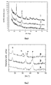
- Fig. 4 represents the GIXRD patterns of the annealed dielectric stack composed of (1) 15nm LaAlO 3 / 10nm ⁇ - Al 2 O 3 and (2) 12nm LuAlO 3 / 15nm LaAlO 3 / 10nm ⁇ -Al 2 O 3 , showing that both LaAlO 3 and LuAlO 3 have crystallized into the perovskite phase.
- Fig. 5 represents the GIXRD patterns of the annealed dielectric stack composed of (1) 15nm LaAlO 3 / 10nm ⁇ - Al 2 O 3 and (2) 12nm GdAlO 3 / 15nm LaAlO 3 / 10nm ⁇ -Al 2 O 3 , showing that both LaAlO 3 and GdAlO 3 have crystallized into the perovskite phase.
- Fig. 6 represents the GIXRD patterns of the annealed dielectric stack composed of (1) 12nm GdAlO 3 /15nm LaAlO 3 /10nm ⁇ -Al 2 O 3 , (2) 12nm GdAlO 3 /15nm SrTiO 3 (STO) as deposited, and (3) 12nm GdAlO 3 /15nm SrTiO 3 (STO) annealed.
- Fig. 7 represents the GIXRD patterns of the annealed (1050°C, 30s, N 2 ) dielectric stack composed of 12 nm LuAlO 3 on a scaled LaAlO 3 / ⁇ -Al 2 O 3 template: (1) 4nm LaAlO 3 / 4nm ⁇ -A1 2 O 3 ; (2) 4nm LaAlO 3 / 3nm ⁇ -Al 2 O 3 ; (3) 3 nm LaAlO 3 / 4nm ⁇ - Al 2 O 3 , wherein 'p' indicates a perovskite peak and 'h' a hexagonal peak.
- Fig. 8 represents the GIXRD patterns of the annealed (950°C, 30s, N 2 ) dielectric stack composed of 12 nm GdAlO 3 and a scaled STO template: (1) 4 nm STO; (2) 3 nm STO; (3) 2 nm STO.
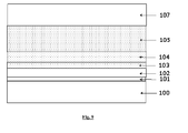
- Fig. 9 represents schematically the dielectric stack of the disclosure in a typical flash memory configuration: substrate/channel region (100), tunnel insulating layer (1O1), charge trapping layer (102), lower template layer (103) upper template layer (104), REAlO 3 dielectric (blocking) layer (105), control electrode (107).
- Fig. 10 represents schematically the dielectric stack of the disclosure in a typical flash memory configuration: substrate/channel region (200), tunnel insulating layer (201), charge trapping layer (202), upper template layer (203), REAlO 3 dielectric (blocking) layer (205), control electrode (207).
- An aim of the present disclosure is to provide a dielectric layer made of rare-earth aluminate with a perovskite structure.
- Another aim is to provide dielectric stack comprising the rare-earth aluminate with a perovskite structure, the dielectric stack being suitable to be used in a flash memory device and having improved performance with respect to the state of the art.
- Yet another aim is to provide a method of manufacturing of the dielectric stack comprising a rare-earth aluminate with a perovskite structure.
- Rare-earth aluminates are dielectric materials (oxides) comprising at least one rare-earth element (RE), aluminum (Al) and oxygen.
- Rare earth elements or rare earth metals are a collection of seventeen chemical elements in the periodic table, namely scandium (Sc), yttrium (Y), and the fifteen lanthanides(Ln): lanthanum (La), cerium (Ce), praseodymium (Pr), neodymium (Nd), promethium (Pm), samarium (Sm), europium (Eu), gadolinium (Gd), terbium (Tb), dysprosium (Dy), holmium (Ho), erbium (Er), thulium (Tm), ytterbium (Yb) and lutetium (Lu).
- the term REAlO 3 is also meant to refer to rare-earth aluminates (RE x Al 2 - x O 3 , with 0 ⁇ x ⁇ 2) .
- Charge trap memory devices comprising a blocking insulating layer made of a material consisting of a lanthanide (Ln), aluminum and oxygen have been previously disclosed.
- Ln lanthanide
- AlO lanthanum-aluminate
- simply replacing lanthanum with another lanthanide or rare-earth element in the lanthanum-aluminate (LaAlO) material of the dielectric (blocking) layer does not necessarily improve the characteristics of the blocking layer such as the dielectric permittivity (k-value) and the band gap value.
- the K -value and the band gap of the rare-earth aluminate compounds depend both on the rare-earth element comprised and on the crystalline structure of the rare-earth aluminate.
- a rare-earth aluminate (RE x Al 2-x O 3 , 0 ⁇ x ⁇ 2) dielectric layer having a perovskite crystalline structure at temperatures compatible with semiconductor manufacturing, wherein the rare-earth aluminate comprises a rare-earth element (RE) having an atomic number higher or equal with 63 (Eu) and lower or equal with 71 (Lu).
- RE rare-earth element
- a dielectric layer having a perovskite crystalline structure at temperatures compatible with semiconductor manufacturing is meant to express that the dielectric layer has a perovskite crystalline structure which is stable (i.e. substantially unaffected) at temperatures lower than 1400°C, preferably lower than 1200°C, more preferably lower than 900°C.
- the RE element can be selected from the group consisting of Eu, Gd, Tb, Dy, Ho, Er, Tm, Yb , Lu, and any combinations or mixtures thereof.
- Rare-earth aluminates comprising two or more rare-earth (RE) elements from the group above are also part of the disclosure.
- a material having a perovskite structure is any material with the same type of crystal structure as calcium titanium oxide (CaTiO3), known as the perovskite structure.
- the general chemical formula for perovskite compounds is ABX3, where 'A' and 'B' are two cations of very different sizes, and X is an anion that bonds to both.
- the 'A' atoms are larger than the 'B' atoms.
- the ideal cubic-symmetry structure has the B cation in 6-fold coordination, surrounded by an octahedron of anions, and the A cation in 12-fold cuboctahedral coordination.
- the perovskite structure is adopted by many oxides that have the chemical formula AB03.
- type 'A' atom sits at cube corner positions (0, 0, 0)
- type 'B' atom sits at body centre position (1/2, 1/2, 1/2)
- oxygen atoms sit at face centered positions (1/2, 1/2, 0).
- the orthorhombic and tetragonal phases are most common non-cubic variants.
- a REAlO 3 in a perovskite phase is not straightforward, especially in the case of the rare-earth aluminates comprising a rare-earth element with a high atomic number. Some of these rare-earth aluminates do not show stable perovskites structures at temperatures compatible with semiconductor manufacturing (e.g. lower than 1400°C, preferably lower than 1200°C). For example, the perovskite phase for LuAlO 3 is only stable above 1800°C (in bulk). Moreover, little is known about REAlO 3 crystallization behavior in thin films (as they are needed for manufacturing semiconductor devices), since phase diagrams are available only for bulk materials.
- the rare-earth aluminate dielectric layer (RE x Al 2-x O 3 , 0 ⁇ x ⁇ 2) having a perovskite structure is preferably a thin film having a thickness lower than few microns, more preferably lower than 1 ⁇ m.
- its thickness is preferably lower than 100nm, more preferably lower than 30nm, even more preferably lower than 20nm.
- the rare-earth aluminate dielectric layer of the disclosure has a stable perovskite crystalline structure at temperatures compatible with semiconductor manufacturing, i.e. at temperatures lower than 1400°C, preferably lower than 1200°C, more preferably lower than 900°C.
- the rare-earth aluminate (PE x Al 2-x O 3 , 0 ⁇ x ⁇ 2) dielectric layer with a perovskite structure has a RE/Al ratio of about 1 (or x is about 1). Both the Al-rich and the RE-rich rare-earth aluminates tend to form other crystalline phases than perovskite.
- the band-gap and the dielectric permittivity (k-value) of the perovskite rare-earth aluminates are the largest when compared to the corresponding values of other crystalline phases of the same compounds.
- the REAlO 3 dielectric layer with a perovskite structure comprises Lu x Al 2 - x O 3 with x being about 1.
- the REAlO 3 dielectric layer with perovskite structure consists of LuAlO 3 .
- the REAlO 3 dielectric layer with a perovskite structure comprises Gd x Al 2-x O 3 with x being about 1.
- the REAlO 3 dielectric layer with perovskite structure consists of GdAlO 3 .
- a dielectric stack comprising:
- the template stack comprises at least an upper template layer with a perovskite structure.
- the template stack can comprise further a lower template layer having a crystalline structure, wherein the lower template layer is underlying and in contact with the upper template layer.
- the template stack consists of two layers: a lower template layer having a crystalline structure and an upper template layer having a perovskite structure.
- the lower template layer having a crystalline structure and underlying and in contact with the upper template layer determines the crystallization of the upper template layer into a perovskite phase.
- the lower template layer consists of ⁇ -A1203 and the upper template layer consists of LaAlO 3
- the LaAlO 3 upper template has a high K -value, while the ⁇ -A1203 lower template layer can be kept thin, with a minor contribution to the equivalent oxide thickness of the whole dielectric stack.
- the crystalline structure of ⁇ -Al 2 O 3 is often described as a defect cubic spinel structure with vacancies on part of the cation positions.
- Each unit cell contains 32 oxygen and 64/3 aluminum ions to fulfill stoichiometry.
- the template stack consists of an upper template layer with a perovskite structure.
- the upper template layer can be made of any crystalline material having a perovskite structure at temperatures compatible with semiconductor manufacturing, or being capable to crystallize in a perovskite structure at temperatures compatible with semiconductor manufacturing when in contact and overlying with another crystalline material (lower template layer).
- Suitable crystalline material for use herein may be easily identified by those skilled in the art in the light of the present disclosure.
- the crystalline material of the upper template layer should preferably have dielectric properties which make it suitable to be used in a dielectric stack of a semiconductor device, in particular of a flash memory device.
- the upper template layer comprises SrTiO 3 (STO) having a perovskite structure.
- the upper template layer consists of SrTiO 3 having a perovskite structure.
- Fig. 1 represents the band gap values (eV) of the rare-earth aluminates as a function of the rare-earth element (i.e. the number of electrons in the f orbitals).
- the simulated (predicted) band gap values for the perovskite structures of the different REAlO 3 are represented by small full dots at the edge of the RE d -Al p band (light grey upper region).
- the energy values of RE f-empty band and the RE f-occupied band are represented by empty- and respectively full - light grey rectangles.
- Fig. 1 shows that the band-gap values are increasing with the atomic number or the number of electrons in the f orbitals.
- the measured band gap values (by e.g. X-ray photoelectron -Electron Energy Loss Spectroscopy, XPS-EELS) for GdAlO 3 and, respectively, LuAlO 3 are represented in Fig. 1 by big full circles (perovskite phase) and big empty circles (hexagonal phase).
- the band gaps of perovskite RE aluminates are larger by more than leV (1.3 for LuAlO 3 and, respectively, 1.0eV for GdAlO 3 ) than those of the hexagonal RE aluminates for the same rare-earth element and the same RE/Al composition.
- the measured band gaps of the perovskite phases are still slightly lower than the predicted ones (small dots surrounded by dotted circle in case of GdAlO 3 and LuAlO 3 ) or than those found experimentally for bulk crystals. Without wishing to be bound by theory, it is believed this is explained by the influence of defects in thin layers.
- hexagonal phases of the REAlO 3 are formed (crystallized) on silicon nitride (Si 3 N 4 , 6nm).
- Fig. 2 represents the equivalent oxide thickness (EOT) of the hexagonal LuAlO 3 (1), hexagonal GdAlO 3 (2), perovskite LuAlO 3 (3) and perovskite GdAlO 3 (4) layers as function of the actual (physical) thickness of the layer.
- EOT equivalent oxide thickness
- the dielectric permittivity is extracted for the perovskite phases of LuAlO 3 and GdAlO 3 and, respectively, for the hexagonal phases of the same compounds. As shown in Table 1, the ⁇ -values of the perovskite RE-aluminates are higher than those of the hexagonal phases. Table 1 ⁇ -value Hexagonal Perovskite GdAlO 3 14 23 LuAlO 3 10 13
- Fig. 1 and Fig. 2 show that, for each rare-earth element, the perovskite structure of the REAlO 3 is having the highest band gap and the highest ⁇ -value when compared with the corresponding values of the hexagonal phase. Further, based on the band gap value and the ⁇ -value, a class of rare-earth aluminates having perovskite structure emerges as particularly suitable to be implemented as dielectric blocking layers in flash memory devices.
- the perovskite rare-earth aluminates REAlO 3 comprising rare-earth elements with an atomic number higher or equal with 63 (Eu) and lower or equal with 71 (Lu) have a band gap higher than 6.4eV and a ⁇ -value higher than 12 which makes them suitable to be implemented as dielectric (blocking) layers in flash memory devices.
- the perovskite phase of LaAlO 3 can be obtained by annealing from the amorphous phase when grown/deposited on ⁇ -Al 2 O 3 as shown in Fig. 4 (curvel) and Fig. 5 (curve 1).
- the rare-earth aluminates comprising Gd or Lu do not crystallize in a perovskite structure when crystallized from an amorphous layer deposited directly (overlying and in contact) on a ⁇ -Al 2 O 3 layer, in contrast with the behavior of LaAlO 3 .
- a similar behavior is expected from the other rare-earth elements with a high atomic number Z, i.e. a Z value between 63 and 71.
- the template stack consists of an upper template layer with a perovskite structure.
- the upper template layer is made of crystalline SrTiO 3 having a perovskite or a similar crystalline structure.
- An amorphous rare-earth aluminate deposited on perovskite SrTiO 3 crystallizes in a perovskite structure having a higher ⁇ -value and a larger band gap than the ⁇ value and, respectively, the band gap of the e.g. hexagonal rare-earth aluminate.
- a SrTiO 3 perovskite upper template layer has a very large dielectric permittivity ( ⁇ -value) of about 100-300, depending on composition and crystallinity, which contributes to the improved dielectric properties of the whole dielectric stack.
- ⁇ -value dielectric permittivity
- the somewhat lower band gap of SrTiO 3 is not a real drawback since the upper template layer is positioned at the bottom of the dielectric stack, underlying a layer with a higher band gap value, i.e. a REAlO 3 dielectric layer, which is functioning as a dielectric blocking layer.
- both the upper and the lower template layer as parts of the template stack should be made as thin as possible to minimize their contribution to the ⁇ -value and band gap value of the whole dielectric stack.
- the thickness of the lower template layer is lower 10 nm, preferably lower than 6 nm.
- the thickness of ⁇ -Al 2 O 3 is preferably lower than 6 nm to minimize its contribution to the EOT of the whole dielectric stack.
- a minimum thickness of about 4 nm ⁇ -A1 2 O 3 shall be preferably respected.
- an unwanted hexagonal phase is (or may be) appearing in the LaAlO 3 upper template for ⁇ -Al 2 O 3 lower template layers thinner than 4nm.
- the EOT contribution of the ⁇ -Al 2 O 3 / LaAlO3 template stack is about 2nm or higher.
- the upper template layer (e.g. perovskite LaAlO 3 ) has a thickness lower than 10nm, preferably lower than 6 nm.
- a minimum thickness of about 4nm is preferably respected for the optimum working of the upper template, i.e. the upper template layer to induce the perovskite structure in the REAlO 3 dielectric layer during crystallization.
- the thickness of SrTiO 3 is preferably lower than 10 nm, more preferably lower than 6nm, even more preferably about 2 nm.
- the EOT contribution of the STO upper template layer to the EOT of the whole dielectric stack is very small.
- the thickness of the rare-earth aluminate dielectric layer is between 10nm and 24nm, preferably between 12nm and 15nm.
- the upper and the lower template layers, the REAlO 3 dielectric layer and the other (optional) layers comprised in the dielectric stack are deposited by Atomic Layer Deposition (ALD) or a Chemical Vapor Deposition (CVD) technique such as Metal-organic Chemical Vapor Deposition (MOCVD) or grown by Molecular Beam Epitaxy (MBE).
- ALD Atomic Layer Deposition
- CVD Chemical Vapor Deposition
- MOCVD Metal-organic Chemical Vapor Deposition
- MBE Molecular Beam Epitaxy
- 10nm Al 2 O 3 was deposited by ALD on a Si substrate, followed by crystallization at about 850°C for about 30s in N 2 ambient to form ⁇ -Al 2 O 3 . Thereafter, 15 nm LaAlO 3 was deposited by ALD on the crystallized ⁇ -Al 2 O 3 and annealed at about 1000°C for about 30s in N 2 ambient to form perovskite LaAlO 3 - Overlying the perovskite LaAlO 3 , 12nm LuAlO 3 and, respectively in another example, 12nm GdAlO 3 was deposited by ALD followed by annealing at about 1050°C for about 30s in N 2 ambient to form perovskite LuAlO 3 and, respectively, perovskite GdAlO 3 .
- Fig. 4 represents the GIXRD pattern of the annealed dielectric stack composed of (from top to bottom): (1) 15nm LaAlO 3 / 10nm ⁇ -Al 2 O 3 and (2) 12nm LuAlO 3 / 15nm LaAlO 3 / 10nm ⁇ -Al 2 O 3 .
- the patterns in Fig. 4 show that both LaAlO 3 and LuAlO 3 crystallized into the perovskite phase.
- Fig. 5 represents the GIXRD pattern of the annealed dielectric stack composed of (from top to bottom): (1) 15nm LaAlO 3 / 10nm ⁇ -Al 2 O 3 and (2) 12nm GdAlO 3 / 15nm LaAlO 3 / 10nm ⁇ -Al 2 O 3 .
- the patterns in Fig 5 show that both LaAlO 3 and GdAlO 3 crystallized into the perovskite phase.
- TEM pictures of REAlO 3 /LaAlO 3 / ⁇ -Al 2 O 3 dielectric stacks show separate REAlO 3 and LaAlO 3 layers and continuity of the crystalline planes and of the crystal orientation through the REAlO 3 /LaAlO 3 interface, for both rare-earth elements (Gd and Lu).
- the crystallized template layer (LaAlO 3 ) is thinner than the as grown/deposited layer because of densification during annealing.
- XPS X-ray Photoelectron Spectroscopy
- 15nm SrTiO 3 template was deposited by ALD on a substrate, followed by crystallization at about 600°C for 1 min in N 2 ambient to form perovskite SrTiO 3 . Thereafter, 12nm GdAlO 3 was deposited by ALD on the crystallized perovskite SrTiO 3 and then annealed at about 1000°C for about 30s in N 2 ambient to form perovskite GdAlO 3 .
- Fig 6 represents the GIXRD patterns of the annealed dielectric stack composed (from top to bottom) of (1) 12nm GdAlO3 /15nm LaAlO 3 /10nm ⁇ -Al 2 O 3 , (2) 12nm GdAlO 3 /15nm SrTiO 3 as deposited, and (3) 12nm GdAlO 3 /15nm SrTiO 3 annealed.
- TEM pictures of the annealed (1050°C) STO-comprising dielectric stack show separate layers in case of GdAlO 3 /SrTiO 3 , while in case of LuAlO 3 /SrTiO 3 the layers are not clearly separated. In both cases, continuity of crystalline planes and of the crystal orientation through the REAlO 3/ SrTiO 3 interface is observed. These results are confirmed by the X-ray Photoelectron Spectroscopy (XPS) results. XPS sputter profiles show some inter-diffusion between GdAlO 3 and SrTiO 3 although separate layers can still be defined, while LuAlO 3 and SrTiO 3 seem to fully inter-diffuse.
- XPS X-ray Photoelectron Spectroscopy
- Fig. 7 represents the GIXRD patterns of the annealed (1050°C, 30s, N 2 ) dielectric stack composed of 12 nm LuAlO 3 on a scaled LaAlO 3 / ⁇ -Al 2 O 3 template stack: (1) 4nm LaAlO 3 / 4nm ⁇ -Al 2 O 3 ; (2) 4nm LaAlO 3 / 3nm ⁇ -Al 2 O 3 ; (3) 3 nm LaAlO 3 / 4nm ⁇ -A1 2 O 3 , wherein ⁇ p ' indicates a peak corresponding to the perovskite phase and ⁇ h ' a peak corresponding to the hexagonal phase.
- the LaAlO 3 / ⁇ -Al 2 O 3 template stack can be scaled down to lower thicknesses. However there is a lower limit for both upper and lower template layers (about 4nm each) that guarantees the optimum working of the template stack.
- curve (1) represents a perovskite structure
- curve (2) and (3) show the presence of peaks that correspond to a hexagonal structure next to the perovskite one.
- the SrTiO 3 (STO) upper template layer can be scaled down successfully to lower thicknesses such as to comply with the most stringent scaling requirements of the flash memory devices.
- Fig. 8 represents the GIXRD patterns of the annealed (950°C, 30s, N 2 ) dielectric stack composed of 12 nm GdAlO 3 and a scaled STO upper template layer: (1) 4 nm STO; (2) 3 nm STO; (3) 2 nm STO. As shown, the STO upper template layer can be perfectly scaled down up to 2nm.
- a semiconductor device comprising a rare-earth aluminate dielectric layer
- the REAlO 3 dielectric layer has a perovskite crystalline structure at temperatures compatible with semiconductor manufacturing and wherein the rare-earth aluminate comprises a rare-earth element (RE) having an atomic number higher or equal with 63 (Eu) and lower or equal with 71 (Lu).
- RE rare-earth element
- the semiconductor device comprises further:
- a flash memory device comprising the REALO 3 dielectric layer, wherein the REAlO 3 dielectric layer has a perovskite crystalline structure at temperatures compatible with semiconductor manufacturing and wherein the rare-earth aluminate comprises a rare-earth element (RE) having an atomic number higher or equal with 63 (Eu) and lower or equal with 71 (Lu).
- RE rare-earth element
- the flash memory device comprises further:
- the flash memory device may comprise other dielectric and/or conductive layers as described further herein.
- Fig. 9 represents schematically a dielectric stack in a typical flash memory configuration: substrate/channel region (100), tunnel insulating layer (101), charge trapping layer (102), lower template layer (103) upper template layer (104), REAlO 3 dielectric (blocking) layer (105), control electrode (107).
- Fig. 10 represents schematically another dielectric stack in a typical flash memory configuration: substrate/channel region (200), tunnel insulating layer (201), charge trapping layer (202), upper template layer (203), REAlO 3 dielectric (blocking) layer (205), control electrode (207).
- the tunnel insulating layer (101, 201) may be a tunneling oxide layer.
- the tunnel insulating layer may be formed of SiO 2 , high- ⁇ dielectric layer or combinations thereof.
- the tunnel insulating layer may be formed of silicon nitride (Si 3 N 4 ) .
- the charge trapping layer (102, 202) may trap charges such as to store information.
- the charge trapping layer may be formed of polysilicon, nitride, a high- ⁇ dielectric material or may include a plurality of nanodots functioning as charge trap sites.
- the control electrode (107, 207) may be formed of a metal layer.
- the gate electrode can be formed of Al, TaN or a metal silicide (e.g. NiSi).
- a cap layer (106, 206. not shown) can be inserted in between the REAlO 3 dielectric (blocking) layer (105, 205) and the control electrode (107, 207).
- the cap layer can be made of dielectric material with a high- ⁇ value which improves the interface properties between the REAlO 3 dielectric (blocking) layer and the control electrode.
- a method for manufacturing a dielectric stack comprising the following steps:
- annealing the substrate comprising the lower template layer, thereby forming a crystalline gamma-alumina is performed at a temperature between 850°C and 1100°C, preferably at about 850°C for a duration of about 30s in N 2 ambient.
- the upper template layer is deposited on the crystallized gamma-alumina and consists of LaAlO 3 .
- annealing the substrate comprising the upper template layer, thereby forming a crystalline LaAlO 3 with a perovskite structure is performed at a temperature between 950°C and 1100°C, preferably at about 1000°C for about 30s in N 2 ambient.
- annealing the substrate comprising the rare-earth aluminate dielectric layer, thereby forming a crystalline REAlO 3 with a perovskite structure is preferably performed at a temperature between about 950°C and about 1050°C, more preferably at 1050°C for about 30s in N 2 ambient.
- annealing to form perovskite GdAlO 3 is preferably performed at a temperature between 780°C and 1050°C.
- annealing to form perovskite LuAlO 3 is preferably performed at a temperature between 910°C and 1050°C.
- the duration of the different thermal treatment (anneal) steps can be between Is to several minutes, most preferably between 30s and 1 minute.
- the ambient can be O 2 , N 2 or any other inert gas (noble gas such as Ar, He).
- the thermal treatments at step (d) and step (f) as above-described can be performed simultaneously, after forming (depositing) the rare-earth aluminate layer (step (e)).
- the total processing time is shortened, which is very important for manufacturing.
- the method for manufacturing a dielectric stack comprises the following steps:
- annealing the substrate comprising a SrTiO 3 upper template layer, thereby forming a crystalline SrTiO 3 with a perovskite structure is performed at a temperature between 600°C and 800°C, for a duration of 30 s in N 2 ambient.
- the anneal temperature required depends on the thickness of the STO layer, e.g. for a thin layer of about 2nm the anneal temperature should be about 800°C.
- annealing the substrate comprising the rare-earth aluminate dielectric layer, thereby forming a crystalline REAlO 3 with a perovskite structure is preferably performed at a temperature between about 930°C and 1000°C for a duration of about 30s in N 2 ambient. A temperature above 1000°C is not recommended since the STO template layer is not stable above this temperature.
- the REAlO 3 dielectric layer consists of LuAlO 3 .
- the REAlO 3 dielectric layer consists of GdAlO 3 .
- annealing to form perovskite GdAlO 3 is preferably performed at a temperature between 830°C and 1000°C.
- annealing to form perovskite LuAlO 3 is preferably performed at a temperature between 930°C and 1000°C.
- dielectric materials having a perovskite structure or having the capability to crystallize in a perovskite structure at temperatures compatible with the semiconductor manufacturing, when overlying and in contact with a crystalline dielectric (a lower template layer) can be used as an upper template layer.
- a crystalline dielectric a lower template layer
- Such alternative dielectric materials suitable for use herein may be easily identified by those skilled in the art of semiconductor processing in the light of the present disclosure.
- a method for manufacturing a dielectric stack comprising the following steps:
- the thermal treatments at step (b) and step (d) of the method can be performed simultaneously, after forming (depositing) the REAlO 3 layer (step (c)).
- the total processing time is shortened, which is very important for manufacturing.
- the present invention relates to the use of a dielectric layer or a dielectric stack as described above in the manufacture of a semiconductor device, preferably a flash memory device.
Landscapes
- Semiconductor Memories (AREA)
- Formation Of Insulating Films (AREA)
- Non-Volatile Memory (AREA)
- Inorganic Insulating Materials (AREA)
Abstract
Description
- The present invention relates to the manufacturing of semiconductor devices. More specifically, the present invention is directed to rare-earth aluminate dielectric material and layer which are particularly suitable for non-volatile memory applications and in particular for integration in flash memory devices.
- For future scaling of flash (non-volatile) memory devices, the inter-poly dielectric or blocking dielectric layers should be made of a dielectric material with a higher K-value than Al2O3 and, at the same time, a band gap comparable or preferably larger than Al2O3. A class of materials that may be able to fulfill these requirements is the class of rare-earth (lanthanide) aluminates, i.e. alloys of rare-earth oxides with Al2O3.
-
US2008/0185633A1 discloses a charge trap memory device comprising: a tunnel insulating layer on a substrate; a charge trap layer on the tunnel insulating layer; and a blocking insulating layer on the charge trap layer, wherein the blocking insulating layer may be formed of a material including a lanthanide (Ln) so as to have a higher dielectric constant and a larger energy band-gap. Ln may refer to the 15 elements ranging from lanthanum (La) as the 57th element to lutetium (Lu) as the 71st element. The blocking insulating layer may further include aluminum and oxygen, wherein the ratio of lanthanide to aluminum may be greater than 1 (e.g., about 1.5 to about 2). - In particular, the application discloses LaAlO having an energy band-gap and a dielectric permittivity (k) depending on the La/Al composition. LaAlO3 with a La/Al composition ratio of 1 may have an energy band-gap of about 5.65 eV and a dielectric permittivity (k) of about 12, while La4Al2O9 with a La/Al composition ratio of 2 may have an energy band-gap of about 5.95 eV and a dielectric constant of about 20.
- Although the performance of the lanthanum aluminates (LaAlO) disclosed in
US2008/0185633A1 is superior to alumina in terms of dielectric permittivity (k-value of thin film γ-Al2O3 is about 9), the band gap achieved is lower than that of thin film γ-Al2O3 (about 6.0 -6.5 eV) and still too low for the most advanced flash memory devices. - There is therefore still a need for a dielectric material and layer, and for a process of manufacturing thereof, wherein the dielectric material possesses a k-value higher than Al2O3 whilst providing a band gap comparable or preferably larger than Al2O3.
- Advantageously, the dielectric material and layer according to the invention allow manufacturing semiconductor devices, in particular flash memory devices, with improved performance and characteristics.
- Other advantages and benefits provided by the dielectric material and layer according to the invention, will be apparent from the following description and the accompanying drawings.
- According to one aspect, the present invention relates to a dielectric layer comprising (or consisting essentially of) (or consisting of) a rare-earth aluminate (RExAl2-xO3 with 0<x<2) and having a (stable) perovskites crystalline structure, wherein the rare-earth aluminate comprises (or consists of) a rare-earth element having an atomic number higher than or equal to (about) 63 and lower than or equal to (about) 71.
- Preferably, the dielectric layer of the invention comprises (or consists of) a rare-earth aluminate (RExAl2-xO3 with 0<x<2), wherein the rare-earth element (RE) is selected from the group consisting of Eu, Gd, Tb, Dy, Ho, Er, Tm, Yb, Lu, and any combinations or mixtures thereof. More preferably, the rare-earth element (RE) is selected from the group consisting of Gd, Lu, and any combinations or mixtures thereof. More preferably, the rare-earth element (RE) is selected to be Gd or Lu.
- Preferably, the dielectric layer of the invention comprises (or consists of) a rare-earth aluminate (RExAl2-xO3 with 0<x<2) which has a perovskite crystalline structure and which is stable at temperatures lower than (about) 1400°C, preferably lower than (about) 1200°C, more preferably lower than (about) 900°C.
- Preferably, the dielectric layer of the invention comprising (or consisting of) a rare-earth aluminate (RExAl2-XO3 with 0<x<2) comprises (or consists of) GdAlO3.
- Preferably still, the dielectric layer of the invention comprising (or consisting of) a rare-earth aluminate (RExAl2-xO3 with 0<x<2) comprises (or consists of) LuAlO3 .
- Preferably, the dielectric layer of the invention has a thickness lower than (about) 5 µm, preferably lower than (about) 1 µm, more preferably lower than (about) 500 nm, even more preferably lower than (about) 100 nm, still more preferably lower than (about) 50 nm, still more preferably lower than (about) 30 nm, still more preferably lower than (about) 20 nm. Preferably still, the dielectric layer of the invention has a thickness comprised between (about) 5 nm and (about) 30 nm, more preferably between (about) 10 nm and (about) 25 nm, still more preferably between (about) 10 nm and (about) 24 nm, still more preferably between (about) 10 nm and (about) 15 nm, still more preferably between (about) 12 nm and (about) 15 nm.
- Preferably, the dielectric layer of the invention comprises (or consists of) a rare-earth aluminate (RExAl2-xO3 with 0<x<2) which has a band gap higher than (about) 5.5 eV, preferably higher than (about) 6.0 eV, more preferably higher than (about) 6.4 eV, even more preferably higher than (about) 6.4 eV, still more preferably higher than (about) 6.5 eV, still more preferably higher than (about) 7.0 eV, still more preferably higher than (about) 7.5 eV.
- Preferably, the dielectric layer of the invention comprises (or consists of) a rare-earth aluminate (RExAl2-xO3 with 0<x<2) which has a K-value higher than (about) 10, preferably higher than (about) 12, more preferably higher than (about) 15, even more preferably higher than (about) 18, still more preferably higher than (about) 20, still more preferably higher than (about) 22, still more preferably higher than (about) 25.
- Preferably, the dielectric layer of the invention comprises (or consists of) a rare-earth aluminate (RExAl2-xO3 with 0<x<2) wherein the RE/Al ratio is of about 1, or alternatively said, x is of about 1. According to this specific aspect, the rare-earth aluminate comprised in the dielectric layer of the invention has the structure REAlO3.
- According to another aspect, the present invention relates to a dielectric stack comprising a dielectric layer as defined above.
- Preferably, the dielectric stack of the invention further comprises a template stack comprising at least an upper template layer, wherein the upper template layer has a perovskite structure, and wherein the upper template layer is underlying and in contact with the rare-earth aluminate (RExA12-xO3 with 0<x<2) dielectric layer.
- Preferably, the dielectric stack of the invention further comprises a lower template layer having a crystalline structure, wherein the lower template layer is underlying and in contact with the upper template layer.
- Preferably, in the dielectric stack of the invention, the lower template layer has a thickness lower than (about) 10 nm, more preferably lower than (about) 6 nm. Preferably still, in the dielectric stack of the invention, the lower template layer has a thickness higher than (about) 4 nm.
- Preferably, in the dielectric stack of the invention, the upper template layer has a thickness lower than (about) 10 nm, more preferably lower than (about) 6 nm, even more preferably lower than (about) 5 nm. Preferably still, in the dielectric stack of the invention, the upper template layer has a thickness higher than (about) 4 nm.
- According to one preferred aspect, in the dielectric stack of the invention, the lower template layer comprises (or consists of) γ-Al2O3.
- According to one preferred aspect, in the dielectric stack of the invention, the upper template layer comprises (or consists in) LaAlO3.
- According to another preferred aspect, in the dielectric stack of the invention, the upper template layer comprises (or consists of) SrTiO3- According to this preferred aspect of the dielectric stack of the invention, the upper template layer has preferably a thickness lower than (about) 10 nm, more preferably lower than (about) 6 nm, even more preferably lower than (about) 4 nm, still more preferably of (about) 2 nm.
- According to another aspect of the present invention, it is provided a method for manufacturing a dielectric stack on a substrate, wherein the method comprises (or consists in) the steps of:
- (a) forming an upper template layer overlying the substrate;
- (b) applying a thermal treatment to the upper template layer overlying the substrate, thereby forming a crystalline upper template layer having a perovskite structure;
- (c) forming a dielectric layer comprising (or consisting of) a rare-earth aluminate (REXAl2-XO3 with 0<x<2) overlying the crystalline upper template layer, wherein the rare-earth aluminate (RExAl2-xO3 with 0<x<2) comprises (or consists of) a rare-earth element having an atomic number higher than or equal to (about) 63 and lower than or equal to (about) 71; and
- (d) applying a thermal treatment to the dielectric layer overlying the crystalline upper template layer, thereby forming a crystalline rare-earth aluminate (RExAl2-xO3 with 0<x<2) dielectric layer having a perovskite structure.
- Preferably, in the method of the invention, the upper template comprises (or consists of) SrTiO3.
- Preferably, the method for manufacturing a dielectric stack on a substrate according to the invention, comprises (or consists in) the steps of:
- (a) forming an upper template layer overlying the substrate, and wherein the upper template layer comprises (or consists of) SrTiO3;
- (b) applying a thermal treatment to the upper template layer overlying the substrate, thereby forming a crystalline upper template layer comprising (or consisting of) SrTiO3 and having a perovskite structure;
- (c) forming a dielectric layer comprising (or consisting of) a rare-earth aluminate (RExAl2-xO3 with 0<x<2) overlying the crystalline upper template layer, wherein the rare-earth aluminate (RExAl2-xO3 with 0<x<2) comprises (or consists of) a rare-earth element having an atomic number higher than or equal to (about) 63 and lower than or equal to (about) 71; and
- (d) applying a thermal treatment to the dielectric layer overlying the crystalline upper template layer, thereby forming a crystalline rare-earth aluminate (REXAl2-XO3 with 0<x<2) dielectric layer having a perovskite structure.
- Preferably, in the method of the invention, the dielectric layer comprising (or consisting of) a rare-earth aluminate (RExAl2-xO3 with 0<x<2) comprises (or consists of) GdAlO3.
- Preferably still, in the method of the invention, the dielectric layer of the invention comprising (or consisting of) a rare-earth aluminate (RExAl2-xO3 with 0<x<2) comprises (or consists of) LuAlO3.
- Preferably, in the method of the invention, the thermal treatment (applied to the upper template layer) at step (b) and the thermal treatment (applied to the dielectric layer overlying the crystalline upper template layer) at step (d) as above-described are performed simultaneously, after step (c) of forming the dielectric layer comprising (or consisting of) a rare-earth aluminate (REXAl2-XO3 with 0<x<2).
- Preferably, in the method of the invention, the thermal treatment (applied to the upper template layer) at step (b) is performed at a temperature comprised between (about) 600°C and (about) 800°C.
- Preferably, in the method of the invention, the thermal treatment (applied to the dielectric layer overlying the crystalline upper template layer) at step (d) is performed at a temperature comprised between (about) 830°C and (about) 1000°C.
- According to the particular aspect of the method of the invention wherein the dielectric layer comprising a rare-earth aluminate (RExAl2-xO3 with 0<x<2) comprises (or consists of) GdAlO3, the thermal treatment (applied to the dielectric layer overlying the crystalline upper template layer) at step (d) is performed at a temperature comprised between (about) 830°C and (about) 1000°C.
- According to the particular aspect of the method of the invention wherein the dielectric layer comprising a rare-earth aluminate (RExAl2-xO3 with 0<x<2) comprises (or consists of) LuAlO3, the thermal treatment (applied to the dielectric layer overlying the crystalline upper template layer) at step (d) is performed at a temperature comprised between (about) 930°C and (about) 1000°C.
- Preferably, in the method of the invention, the thermal treatment (applied to the upper template layer) at step (b) and the thermal treatment (applied to the dielectric layer overlying the crystalline upper template layer) at step (d) are annealing treatments.
- Preferably, in the method of the invention, the thermal treatment (applied to the upper template layer) at step (b) and the thermal treatment (applied to the dielectric layer overlying the crystalline upper template layer) at step (d) are performed for a duration comprised between (about) 1 second to (about) 5 minutes, preferably between (about) 30 seconds and (about) 1 minute, more preferably for a duration of (about) 30 seconds.
- Preferably, in the method of the invention, the thermal treatment (applied to the upper template layer) at step (b) and the thermal treatment (applied to the dielectric layer overlying the crystalline upper template layer) at step (d) are performed in an ambient selected from the group consisting of O2, N2, inert gases (preferably noble gases such as Ar or He), and any combinations or mixtures thereof. More preferably, the ambient is selected to comprise (or consist of) N2.
- According to another preferred aspect, the method of the invention further comprises the step of forming a lower template layer having a crystalline structure and overlying the substrate, wherein the lower template is underlying and in contact with the upper template layer.
- Preferably, in the method of the invention, the lower template layer having a crystalline structure comprises (or consists of) γ-Al2O3.
- According to one preferred aspect of the method of the invention wherein the lower template layer having a crystalline structure comprises (or consists of) 7-Al2O3, the step of forming a lower template layer having a crystalline structure and overlying the substrate, comprises (or consists in) the steps of:
- forming a lower template layer comprising (or consisting of) amorphous Al2O3 and overlying the substrate; and
- applying a thermal treatment to the lower template layer, thereby forming a crystalline γ-Al2O3 layer.
- Preferably, in the method of the invention, the upper template comprises (or consists of) LaAlO3.
- According to another preferred aspect, the method for manufacturing a dielectric stack on a substrate according to the invention, comprises (or consists in) the steps of:
- (a) forming a lower template layer comprising (or consisting of) amorphous Al2O3 and overlying the substrate;
- (b) applying a thermal treatment to the lower template layer, thereby forming a crystalline gamma-alumina (γ-Al2O3) layer;
- (c) forming an upper template layer overlying the crystalline γ-Al2O3 layer, wherein the upper template layer comprises (or consists of) LaAlO3;
- (d) applying a thermal treatment to the upper template layer overlying the crystalline γ-Al2O3 layer, thereby forming a crystalline LaAlO3 upper template layer having a perovskite structure;
- (e) forming a dielectric layer comprising (or consisting of) a rare-earth aluminate (RExAl2-xO3 with 0<x<2) overlying the crystalline LaAlO3 upper template layer, wherein the rare-earth aluminate (RExAl2-xO3 with 0<x<2) comprises (or consists of) a rare-earth element having an atomic number higher than or equal to (about) 63 and lower than or equal to (about) 71; and
- (f) applying a thermal treatment to the dielectric layer overlying the crystalline LaAlO3 upper template layer, thereby forming a crystalline rare-earth aluminate (RExAl2-xO3 with 0<x<2) dielectric layer having a perovskite structure.
- Preferably, in the method of the invention, the dielectric layer comprising (or consisting of) a rare-earth aluminate (RExAl2-xO3 with 0<x<2) comprises (or consists of) GdAlO3 .
- Preferably still, in the method of the invention, the dielectric layer of the invention comprising (or consisting of) a rare-earth aluminate (RExAl2-xO3 with 0<x<2) comprises (or consists of) LuAlO3.
- Preferably, in the method of the invention, the thermal treatment (applied to the lower template layer) at step (b) above is performed at a temperature comprised between (about) 850°C and (about) 1100°C, preferably at (about) 850°C.
- Preferably, in the method of the invention, the thermal treatment (applied to the upper template layer overlying the crystalline γ-Al2O3 layer) at step (d) above is performed at a temperature comprised between (about) 950°C and (about) 1100°C, preferably at (about) 1000°C.
- Preferably, in the method of the invention, the thermal treatment (applied to the dielectric layer overlying the crystalline LaAlO3 upper template layer) at step (f) above is performed at a temperature comprised between (about) 780°C and (about) 1050°C, preferably between (about) 910°C and (about) 1050°C, more preferably between (about) 950°C and (about) 1050°C, even more preferably at (about) 1050°C.
- According to the particular aspect of the method of the invention wherein the dielectric layer comprising (or consisting of) a rare-earth aluminate (RExAl2-xO3 with 0<x<2) comprises (or consists in) GdAlO3, the thermal treatment (applied to the dielectric layer overlying the crystalline LaAlO3 upper template layer) at step (f) above is performed at a temperature comprised between (about) 780°C and (about) 1050°C.
- According to the particular aspect of the method of the invention wherein the dielectric layer comprising (or consisting of) a rare-earth aluminate (RExAl2-xO3 with 0<x<2) comprises (or consists in) LuAlO3, the thermal treatment (applied to the dielectric layer overlying the crystalline LaAlO3 upper template layer) at step (f) above is performed at a temperature comprised between (about) 910°C and (about) 1050°C.
- Preferably, in the method of the invention, the thermal treatment (applied to the upper template layer overlying the crystalline γ-Al2O3 layer) at step (d) above and the thermal treatment (applied to the dielectric layer overlying the crystalline LaAlO3 upper template layer) at step (f) above are performed simultaneously, after step (e) of forming the dielectric layer comprising a rare-earth aluminate (RExAl2-XO3 with 0<x<2) .
- Preferably, in the method of the invention, the thermal treatment (applied to the lower template layer) at step (b) above, the thermal treatment (applied to the upper template layer overlying the crystalline γ-Al2O3 layer) at step (d) above, and the thermal treatment (applied to the dielectric layer overlying the crystalline LaAlO3 upper template layer) at step (f) above, are annealing treatments.
- Preferably, in the method of the invention, the thermal treatment (applied to the lower template layer) at step (b) above, the thermal treatment (applied to the upper template layer overlying the crystalline γ-Al2O3 layer) at step (d) above, and the thermal treatment (applied to the dielectric layer overlying the crystalline LaAlO3 upper template layer) at step (f) above, are performed for a duration comprised between (about) 1 second to (about) 5 minutes, preferably between (about) 30 seconds and (about) 1 minute, more preferably for a duration of (about) 30 seconds.
- Preferably, in the method of the invention, the thermal treatment (applied to the lower template layer) at step (b) above, the thermal treatment (applied to the upper template layer overlying the crystalline γ-Al2O3 layer) at step (d) above, and the thermal treatment (applied to the dielectric layer overlying the crystalline LaAlO3 upper template layer) at step (f) above, are performed in an ambient selected from the group consisting of O2, N2, inert gases (preferably noble gases such as Ar or He), and any combinations or mixtures thereof. More preferably, the ambient is selected to comprise (or consist of) N2.
- According to still another aspect of the present invention, it is provided a semiconductor device comprising a dielectric layer or a dielectric stack as described above. Preferably, the semiconductor device is a non-volatile memory device, more preferably a flash memory device.
- According to still another aspect, the present invention relates to the use of a dielectric layer or a dielectric stack or a method as described above in the manufacture of a semiconductor device, preferably a flash memory device.
- All drawings are intended to illustrate some aspects and embodiments of the present disclosure. The drawings described are only schematic and are non-limiting.
-
Fig. 1 represents the band gap values (eV) of the rare-earth aluminates as a function of the rare-earth element comprised. -
Fig. 2 represents the equivalent oxide thickness (EOT) of the hexagonal LuAlO3 (1), hexagonal GdAlO3 (2), perovskite LuAlO3 (3) and perovskite GdAlO3 (4) layers as function of the actual (physical) thickness of the same layer. -
Fig. 3 represents the GIXRD (Grazing Incidence X-ray Diffraction) patterns of dielectric stack comprising a layer of LuAlO3 overlying and in contact with y-Al2O3, after annealing at 1000°C (curve 1) and 1100°C (curve 2) for 30s in N2, showing crystallization in a hexagonal phase. -
Fig. 4 represents the GIXRD patterns of the annealed dielectric stack composed of (1) 15nm LaAlO3/ 10nm γ-Al2O3 and (2) 12nm LuAlO3/ 15nm LaAlO3/ 10nm γ-Al2O3, showing that both LaAlO3 and LuAlO3 have crystallized into the perovskite phase. -
Fig. 5 represents the GIXRD patterns of the annealed dielectric stack composed of (1) 15nm LaAlO3/ 10nm γ-Al2O3 and (2) 12nm GdAlO3/ 15nm LaAlO3/ 10nm γ-Al2O3, showing that both LaAlO3 and GdAlO3 have crystallized into the perovskite phase. -
Fig. 6 represents the GIXRD patterns of the annealed dielectric stack composed of (1) 12nm GdAlO3/15nm LaAlO3/10nm γ-Al2O3, (2) 12nm GdAlO3/15nm SrTiO3 (STO) as deposited, and (3) 12nm GdAlO3/15nm SrTiO3 (STO) annealed. -
Fig. 7 represents the GIXRD patterns of the annealed (1050°C, 30s, N2) dielectric stack composed of 12 nm LuAlO3 on a scaled LaAlO3/γ-Al2O3 template: (1) 4nm LaAlO3/ 4nm γ-A12O3; (2) 4nm LaAlO3/ 3nm γ-Al2O3; (3) 3 nm LaAlO3/ 4nm γ-Al2O3, wherein 'p' indicates a perovskite peak and 'h' a hexagonal peak. -
Fig. 8 represents the GIXRD patterns of the annealed (950°C, 30s, N2) dielectric stack composed of 12 nm GdAlO3 and a scaled STO template: (1) 4 nm STO; (2) 3 nm STO; (3) 2 nm STO. -
Fig. 9 represents schematically the dielectric stack of the disclosure in a typical flash memory configuration: substrate/channel region (100), tunnel insulating layer (1O1), charge trapping layer (102), lower template layer (103) upper template layer (104), REAlO3 dielectric (blocking) layer (105), control electrode (107). -
Fig. 10 represents schematically the dielectric stack of the disclosure in a typical flash memory configuration: substrate/channel region (200), tunnel insulating layer (201), charge trapping layer (202), upper template layer (203), REAlO3 dielectric (blocking) layer (205), control electrode (207). - An aim of the present disclosure is to provide a dielectric layer made of rare-earth aluminate with a perovskite structure.
- Another aim is to provide dielectric stack comprising the rare-earth aluminate with a perovskite structure, the dielectric stack being suitable to be used in a flash memory device and having improved performance with respect to the state of the art.
- Yet another aim is to provide a method of manufacturing of the dielectric stack comprising a rare-earth aluminate with a perovskite structure.
- Rare-earth aluminates (RExAl2-xO3, with 0< x< 2) are dielectric materials (oxides) comprising at least one rare-earth element (RE), aluminum (Al) and oxygen. Rare earth elements or rare earth metals are a collection of seventeen chemical elements in the periodic table, namely scandium (Sc), yttrium (Y), and the fifteen lanthanides(Ln): lanthanum (La), cerium (Ce), praseodymium (Pr), neodymium (Nd), promethium (Pm), samarium (Sm), europium (Eu), gadolinium (Gd), terbium (Tb), dysprosium (Dy), holmium (Ho), erbium (Er), thulium (Tm), ytterbium (Yb) and lutetium (Lu). The concentration "x" of the rare-earth element (RE) and of Al in the rare-earth aluminate compound may vary.
- Throughout the disclosure, and unless otherwise specified, the ratio RE/Al is preferably such that RE/Al = 1, or x = 1. However, throughout the present disclosure, the term REAlO3 is also meant to refer to rare-earth aluminates (RExAl2-xO3, with 0< x< 2) .
- Throughout the present description, the expressions "consisting of" or "consisting essentially of" are used interchangeably and are meant to have the same meaning.
- Charge trap memory devices comprising a blocking insulating layer made of a material consisting of a lanthanide (Ln), aluminum and oxygen have been previously disclosed. However, simply replacing lanthanum with another lanthanide or rare-earth element in the lanthanum-aluminate (LaAlO) material of the dielectric (blocking) layer does not necessarily improve the characteristics of the blocking layer such as the dielectric permittivity (k-value) and the band gap value.
- As further disclosed in different embodiments, the K-value and the band gap of the rare-earth aluminate compounds depend both on the rare-earth element comprised and on the crystalline structure of the rare-earth aluminate.
- In a first aspect of the disclosure a rare-earth aluminate (RExAl2-xO3, 0< x < 2) dielectric layer is disclosed having a perovskite crystalline structure at temperatures compatible with semiconductor manufacturing, wherein the rare-earth aluminate comprises a rare-earth element (RE) having an atomic number higher or equal with 63 (Eu) and lower or equal with 71 (Lu).
- In the context of the present invention, the expression "a dielectric layer having a perovskite crystalline structure at temperatures compatible with semiconductor manufacturing" is meant to express that the dielectric layer has a perovskite crystalline structure which is stable (i.e. substantially unaffected) at temperatures lower than 1400°C, preferably lower than 1200°C, more preferably lower than 900°C.
- The RE element can be selected from the group consisting of Eu, Gd, Tb, Dy, Ho, Er, Tm, Yb , Lu, and any combinations or mixtures thereof. Rare-earth aluminates comprising two or more rare-earth (RE) elements from the group above are also part of the disclosure.
- A material having a perovskite structure is any material with the same type of crystal structure as calcium titanium oxide (CaTiO3), known as the perovskite structure. The general chemical formula for perovskite compounds is ABX3, where 'A' and 'B' are two cations of very different sizes, and X is an anion that bonds to both. The 'A' atoms are larger than the 'B' atoms. The ideal cubic-symmetry structure has the B cation in 6-fold coordination, surrounded by an octahedron of anions, and the A cation in 12-fold cuboctahedral coordination. The perovskite structure is adopted by many oxides that have the chemical formula AB03. In the idealized cubic unit cell of such a compound, type 'A' atom sits at cube corner positions (0, 0, 0), type 'B' atom sits at body centre position (1/2, 1/2, 1/2) and oxygen atoms sit at face centered positions (1/2, 1/2, 0). The orthorhombic and tetragonal phases are most common non-cubic variants.
- Manufacturing a REAlO3 in a perovskite phase is not straightforward, especially in the case of the rare-earth aluminates comprising a rare-earth element with a high atomic number. Some of these rare-earth aluminates do not show stable perovskites structures at temperatures compatible with semiconductor manufacturing (e.g. lower than 1400°C, preferably lower than 1200°C). For example, the perovskite phase for LuAlO3 is only stable above 1800°C (in bulk). Moreover, little is known about REAlO3 crystallization behavior in thin films (as they are needed for manufacturing semiconductor devices), since phase diagrams are available only for bulk materials.
- The rare-earth aluminate dielectric layer (RExAl2-xO3, 0< x < 2) having a perovskite structure is preferably a thin film having a thickness lower than few microns, more preferably lower than 1 µm. In one aspect of the invention wherein the rare-earth aluminate dielectric layer is part of a dielectric stack of a flash memory device, its thickness is preferably lower than 100nm, more preferably lower than 30nm, even more preferably lower than 20nm.
- The rare-earth aluminate dielectric layer of the disclosure has a stable perovskite crystalline structure at temperatures compatible with semiconductor manufacturing, i.e. at temperatures lower than 1400°C, preferably lower than 1200°C, more preferably lower than 900°C.
- In one preferred aspect of the invention, the rare-earth aluminate (PExAl2-xO3, 0< x < 2) dielectric layer with a perovskite structure has a RE/Al ratio of about 1 (or x is about 1). Both the Al-rich and the RE-rich rare-earth aluminates tend to form other crystalline phases than perovskite. Advantageously, the band-gap and the dielectric permittivity (k-value) of the perovskite rare-earth aluminates are the largest when compared to the corresponding values of other crystalline phases of the same compounds.
- In one preferred aspect of the invention, the REAlO3 dielectric layer with a perovskite structure comprises LuxAl2-xO3 with x being about 1. In specific aspects of the invention as further described in detail, the REAlO3 dielectric layer with perovskite structure consists of LuAlO3 .
- In another preferred aspect of the invention, the REAlO3 dielectric layer with a perovskite structure comprises GdxAl2-xO3 with x being about 1. In specific aspects of the invention as further described in detail, the REAlO3 dielectric layer with perovskite structure consists of GdAlO3 .
- In a second aspect of the present disclosure a dielectric stack is disclosed, comprising:
- the REAlO3 dielectric layer having a perovskite structure at temperatures compatible with semiconductor manufacturing, wherein the rare-earth aluminate comprises a rare-earth element (RE) having an atomic number higher or equal with 63 (Eu) and lower or equal with 71 (Lu), and
- a template stack comprising at least an upper template layer, wherein the upper template layer has a perovskite structure, and
- wherein the upper template layer is underlying and in contact with the REAlO3 dielectric layer.
- In one aspect of the invention, the template stack comprises at least an upper template layer with a perovskite structure. The template stack can comprise further a lower template layer having a crystalline structure, wherein the lower template layer is underlying and in contact with the upper template layer.
- In a different aspect of the invention, the template stack consists of two layers: a lower template layer having a crystalline structure and an upper template layer having a perovskite structure.
- The lower template layer, having a crystalline structure and underlying and in contact with the upper template layer determines the crystallization of the upper template layer into a perovskite phase.
- In some aspects of the invention, which are illustrated in detail elsewhere in the description, the lower template layer consists of γ-A1203 and the upper template layer consists of LaAlO3 Advantageously, the LaAlO3 upper template has a high K-value, while the γ-A1203 lower template layer can be kept thin, with a minor contribution to the equivalent oxide thickness of the whole dielectric stack.
- The crystalline structure of γ-Al2O3 is often described as a defect cubic spinel structure with vacancies on part of the cation positions. Each unit cell contains 32 oxygen and 64/3 aluminum ions to fulfill stoichiometry.
- In alternative aspects of the invention, the template stack consists of an upper template layer with a perovskite structure.
- The upper template layer can be made of any crystalline material having a perovskite structure at temperatures compatible with semiconductor manufacturing, or being capable to crystallize in a perovskite structure at temperatures compatible with semiconductor manufacturing when in contact and overlying with another crystalline material (lower template layer). Suitable crystalline material for use herein may be easily identified by those skilled in the art in the light of the present disclosure. The crystalline material of the upper template layer should preferably have dielectric properties which make it suitable to be used in a dielectric stack of a semiconductor device, in particular of a flash memory device.
- In one preferred aspect of the invention, the upper template layer comprises SrTiO3 (STO) having a perovskite structure.
- In some preferred aspects of the invention which are illustrated in detail elsewhere in the description, the upper template layer consists of SrTiO3 having a perovskite structure.
-
Fig. 1 represents the band gap values (eV) of the rare-earth aluminates as a function of the rare-earth element (i.e. the number of electrons in the f orbitals). - The simulated (predicted) band gap values for the perovskite structures of the different REAlO3 are represented by small full dots at the edge of the RE d -Al p band (light grey upper region). The energy values of RE f-empty band and the RE f-occupied band are represented by empty- and respectively full - light grey rectangles.
Fig. 1 shows that the band-gap values are increasing with the atomic number or the number of electrons in the f orbitals. - The measured band gap values (by e.g. X-ray photoelectron -Electron Energy Loss Spectroscopy, XPS-EELS) for GdAlO3 and, respectively, LuAlO3 are represented in
Fig. 1 by big full circles (perovskite phase) and big empty circles (hexagonal phase). As shown, the band gaps of perovskite RE aluminates are larger by more than leV (1.3 for LuAlO3 and, respectively, 1.0eV for GdAlO3) than those of the hexagonal RE aluminates for the same rare-earth element and the same RE/Al composition. - As shown in
Fig. 1 , the measured band gaps of the perovskite phases are still slightly lower than the predicted ones (small dots surrounded by dotted circle in case of GdAlO3 and LuAlO3) or than those found experimentally for bulk crystals. Without wishing to be bound by theory, it is believed this is explained by the influence of defects in thin layers. - Photoconductivity measurements show that the hexagonal GdAlO3 has a band gap of 5.5 eV. For higher Gd concentrations, e.g. Gd1.4Al0.6O3 the band gap has a value of about 5.3 eV, while for lower Gd concentrations e.g. Gd0.5Al1.5O3 the band gap has a value of about 5.9 eV. These band gap values are situated in between the band gaps of Gd2O3 (about 5.2 eV) and Al2O3 (about 6.0-6.5eV) and therefore not enough to justify the replacement of Al2O3 in flash memory devices, even when considering the benefits of a higher κ― value of about 12 for 25% Gd to about 18 for 70% Gd.
- Photoconductivity measurements of hexagonal LuxAl2-xO3 shows a band gap of about 6.1 eV, more close to the band gap value of Al2O3, independent of the Lu concentration (x =0.5 to x= 1.5). This band gap value does not justify the replacement of Al2O3 in flash memory devices, especially since the κ-value measured for hexagonal LuAlO3 is about 10, rather low for a significant improvement in the performance of a flash memory devices based hereupon.
- In a particular example, perovskite REAlO3 layers (RE = Gd, Lu) are crystallized on a template stack consisting of a lower template layer of γ-Al2O3 (4nm) and, thereupon an upper template layer of LaAlO3 (5nm). In a comparative example, hexagonal phases of the REAlO3 are formed (crystallized) on silicon nitride (Si3N4, 6nm).
-
Fig. 2 represents the equivalent oxide thickness (EOT) of the hexagonal LuAlO3 (1), hexagonal GdAlO3 (2), perovskite LuAlO3 (3) and perovskite GdAlO3 (4) layers as function of the actual (physical) thickness of the layer. - The dielectric permittivity is extracted for the perovskite phases of LuAlO3 and GdAlO3 and, respectively, for the hexagonal phases of the same compounds. As shown in Table 1, the κ-values of the perovskite RE-aluminates are higher than those of the hexagonal phases.
Table 1 κ-value Hexagonal Perovskite GdAlO 3 14 23 LuAlO 310 13 - The combined interpretation of
Fig. 1 andFig. 2 shows that, for each rare-earth element, the perovskite structure of the REAlO3 is having the highest band gap and the highest κ-value when compared with the corresponding values of the hexagonal phase. Further, based on the band gap value and the κ-value, a class of rare-earth aluminates having perovskite structure emerges as particularly suitable to be implemented as dielectric blocking layers in flash memory devices. - The perovskite rare-earth aluminates REAlO3 comprising rare-earth elements with an atomic number higher or equal with 63 (Eu) and lower or equal with 71 (Lu) have a band gap higher than 6.4eV and a κ-value higher than 12 which makes them suitable to be implemented as dielectric (blocking) layers in flash memory devices.
- The perovskite phase of LaAlO3 can be obtained by annealing from the amorphous phase when grown/deposited on γ-Al2O3 as shown in
Fig. 4 (curvel) andFig. 5 (curve 1). - We surprisingly found out that the rare-earth aluminates comprising Gd or Lu do not crystallize in a perovskite structure when crystallized from an amorphous layer deposited directly (overlying and in contact) on a γ-Al2O3 layer, in contrast with the behavior of LaAlO3. Without wishing to be bound by theory, a similar behavior is expected from the other rare-earth elements with a high atomic number Z, i.e. a Z value between 63 and 71.
- In a comparative example it is shown that GdAlO3 and LuAlO3 crystallize in a hexagonal phase when grown directly on thin SiO2 (SiO2 thin compared to REAlO3), Si3N4, or γ-Al2O3. The GIXRD pattern of LuAlO3/ γ-Al2O3 after annealing at 1000°C (curve 1) and 1100°C (curve 2) shows crystallization in the hexagonal phase, as represented in
Fig. 3 . - In some aspects of the invention, the template stack consists of an upper template layer with a perovskite structure.
- In some aspects of the invention, the upper template layer is made of crystalline SrTiO3 having a perovskite or a similar crystalline structure.
- An amorphous rare-earth aluminate deposited on perovskite SrTiO3 crystallizes in a perovskite structure having a higher κ-value and a larger band gap than the κ― value and, respectively, the band gap of the e.g. hexagonal rare-earth aluminate.
- Advantageously, a SrTiO3 perovskite upper template layer has a very large dielectric permittivity (κ-value) of about 100-300, depending on composition and crystallinity, which contributes to the improved dielectric properties of the whole dielectric stack. The somewhat lower band gap of SrTiO3 is not a real drawback since the upper template layer is positioned at the bottom of the dielectric stack, underlying a layer with a higher band gap value, i.e. a REAlO3 dielectric layer, which is functioning as a dielectric blocking layer.
- In some preferred aspects of the invention, both the upper and the lower template layer as parts of the template stack should be made as thin as possible to minimize their contribution to the κ-value and band gap value of the whole dielectric stack.
- In some preferred aspects of the invention, the thickness of the lower template layer is lower 10 nm, preferably lower than 6 nm.
- In the particular aspect of the invention wherein the lower template layer is made of γ-Al2O3, the thickness of γ-Al2O3 is preferably lower than 6 nm to minimize its contribution to the EOT of the whole dielectric stack.
- Further, for the optimum working of the γ-Al2O3 as lower template layer, i.e. the lower template layer to induce the perovskite structure in the upper template layer (LaAlO3) during crystallization, a minimum thickness of about 4 nm γ-A12O3 shall be preferably respected. Experiments have shown than an unwanted hexagonal phase is (or may be) appearing in the LaAlO3 upper template for γ-Al2O3 lower template layers thinner than 4nm. Depending on the thickness employed, the EOT contribution of the γ-Al2O3/ LaAlO3 template stack is about 2nm or higher.
- In some preferred aspects of the invention, the upper template layer, (e.g. perovskite LaAlO3) has a thickness lower than 10nm, preferably lower than 6 nm.
- In scaled devices it is particularly important to scale down the thickness of the upper template layer as well, up to thicknesses lower than 5nm. Further, a minimum thickness of about 4nm is preferably respected for the optimum working of the upper template, i.e. the upper template layer to induce the perovskite structure in the REAlO3 dielectric layer during crystallization.
- In the alternative aspects wherein the upper template layer consists of SrTiO3, the thickness of SrTiO3 is preferably lower than 10 nm, more preferably lower than 6nm, even more preferably about 2 nm. Advantageously, the EOT contribution of the STO upper template layer to the EOT of the whole dielectric stack is very small.
- In some preferred aspects of the invention, the thickness of the rare-earth aluminate dielectric layer is between 10nm and 24nm, preferably between 12nm and 15nm.
- Preferably, the upper and the lower template layers, the REAlO3 dielectric layer and the other (optional) layers comprised in the dielectric stack are deposited by Atomic Layer Deposition (ALD) or a Chemical Vapor Deposition (CVD) technique such as Metal-organic Chemical Vapor Deposition (MOCVD) or grown by Molecular Beam Epitaxy (MBE).
- In a particular example 10nm Al2O3 was deposited by ALD on a Si substrate, followed by crystallization at about 850°C for about 30s in N2 ambient to form γ-Al2O3. Thereafter, 15 nm LaAlO3 was deposited by ALD on the crystallized γ-Al2O3 and annealed at about 1000°C for about 30s in N2 ambient to form perovskite LaAlO3- Overlying the perovskite LaAlO3, 12nm LuAlO3 and, respectively in another example, 12nm GdAlO3 was deposited by ALD followed by annealing at about 1050°C for about 30s in N2 ambient to form perovskite LuAlO3 and, respectively, perovskite GdAlO3.
-
Fig. 4 represents the GIXRD pattern of the annealed dielectric stack composed of (from top to bottom): (1) 15nm LaAlO3/ 10nm γ-Al2O3 and (2) 12nm LuAlO3/ 15nm LaAlO3/ 10nm γ-Al2O3. The patterns inFig. 4 show that both LaAlO3 and LuAlO3 crystallized into the perovskite phase. LuAlO3 crystallizes into perovskite phase with slightly smaller lattice parameter (a=3.64 Ångstrom) than LaAlO3 (a= 3.76 Ångstrom), shown by the slightly shift of the peaks towards higher angles. No mixing of the two perovskites occurs. -
Fig. 5 represents the GIXRD pattern of the annealed dielectric stack composed of (from top to bottom): (1) 15nm LaAlO3/ 10nm γ-Al2O3 and (2) 12nm GdAlO3/ 15nm LaAlO3/ 10nm γ-Al2O3. The patterns inFig 5 show that both LaAlO3 and GdAlO3 crystallized into the perovskite phase. GdAlO3 crystallizes into perovskite phase with a lattice parameter (a=3.73 Ångstrom), very close to the lattice parameter of LaAlO3 (a= 3.76 Ångstrom). - Transmission Electron Microscopy (TEM) pictures of REAlO3/LaAlO3/γ-Al2O3 dielectric stacks show separate REAlO3 and LaAlO3 layers and continuity of the crystalline planes and of the crystal orientation through the REAlO3/LaAlO3 interface, for both rare-earth elements (Gd and Lu). The crystallized template layer (LaAlO3) is thinner than the as grown/deposited layer because of densification during annealing.
- Consistent with TEM results, XPS (X-ray Photoelectron Spectroscopy) sputter profiles of the GdAlO3/LaAlO3/γ-Al2O3 and LuAlO3/LaAlO3/γ-Al2O3 dielectric stacks show that GdAlO3 and, respectively, LuAlO3 do not inter-diffuse with LaAlO3/Al2O3 template stack.
- Alternatively, in another example, 15nm SrTiO3 template was deposited by ALD on a substrate, followed by crystallization at about 600°C for 1 min in N2 ambient to form perovskite SrTiO3. Thereafter, 12nm GdAlO3 was deposited by ALD on the crystallized perovskite SrTiO3 and then annealed at about 1000°C for about 30s in N2 ambient to form perovskite GdAlO3.
-
Fig 6 represents the GIXRD patterns of the annealed dielectric stack composed (from top to bottom) of (1) 12nm GdAlO3 /15nm LaAlO3/10nm γ-Al2O3, (2) 12nm GdAlO3/15nm SrTiO3 as deposited, and (3) 12nm GdAlO3/15nm SrTiO3 annealed. - Transmission Electron Microscopy (TEM) pictures of the annealed (1050°C) STO-comprising dielectric stack show separate layers in case of GdAlO3/SrTiO3, while in case of LuAlO3/SrTiO3 the layers are not clearly separated. In both cases, continuity of crystalline planes and of the crystal orientation through the REAlO3/SrTiO3 interface is observed. These results are confirmed by the X-ray Photoelectron Spectroscopy (XPS) results. XPS sputter profiles show some inter-diffusion between GdAlO3 and SrTiO3 although separate layers can still be defined, while LuAlO3 and SrTiO3 seem to fully inter-diffuse.
-
Fig. 7 represents the GIXRD patterns of the annealed (1050°C, 30s, N2) dielectric stack composed of 12 nm LuAlO3 on a scaled LaAlO3/γ-Al2O3 template stack: (1) 4nm LaAlO3/ 4nm γ-Al2O3; (2) 4nm LaAlO3/ 3nm γ-Al2O3; (3) 3 nm LaAlO3/ 4nm γ-A12O3, wherein `p' indicates a peak corresponding to the perovskite phase and `h' a peak corresponding to the hexagonal phase. - The LaAlO3/γ-Al2O3 template stack can be scaled down to lower thicknesses. However there is a lower limit for both upper and lower template layers (about 4nm each) that guarantees the optimum working of the template stack. As shown in
Figure 7 , curve (1) represents a perovskite structure, while curve (2) and (3) show the presence of peaks that correspond to a hexagonal structure next to the perovskite one. - Advantageously, the SrTiO3 (STO) upper template layer can be scaled down successfully to lower thicknesses such as to comply with the most stringent scaling requirements of the flash memory devices.
-
Fig. 8 represents the GIXRD patterns of the annealed (950°C, 30s, N2) dielectric stack composed of 12 nm GdAlO3 and a scaled STO upper template layer: (1) 4 nm STO; (2) 3 nm STO; (3) 2 nm STO. As shown, the STO upper template layer can be perfectly scaled down up to 2nm. - In another aspect of the invention, a semiconductor device comprising a rare-earth aluminate dielectric layer is disclosed, wherein the REAlO3 dielectric layer has a perovskite crystalline structure at temperatures compatible with semiconductor manufacturing and wherein the rare-earth aluminate comprises a rare-earth element (RE) having an atomic number higher or equal with 63 (Eu) and lower or equal with 71 (Lu).
- In one preferred aspect of the invention, the semiconductor device comprises further:
- a template stack comprising at least an upper template layer,
- wherein the upper template layer has a perovskite structure, and
- wherein the upper template layer is underlying and in contact with the REAlO3 dielectric layer.
- According to one preferred aspect of the invention, it is provided a flash memory device comprising the REALO3 dielectric layer, wherein the REAlO3 dielectric layer has a perovskite crystalline structure at temperatures compatible with semiconductor manufacturing and wherein the rare-earth aluminate comprises a rare-earth element (RE) having an atomic number higher or equal with 63 (Eu) and lower or equal with 71 (Lu).
- According to one specific execution, the flash memory device comprises further:
- a template stack comprising at least an upper template layer,
- wherein the upper template layer has a perovskite structure, and
- wherein the upper template layer is underlying and in contact with the REAlO3 dielectric layer.
- The flash memory device may comprise other dielectric and/or conductive layers as described further herein.
Fig. 9 represents schematically a dielectric stack in a typical flash memory configuration: substrate/channel region (100), tunnel insulating layer (101), charge trapping layer (102), lower template layer (103) upper template layer (104), REAlO3 dielectric (blocking) layer (105), control electrode (107). -
Fig. 10 represents schematically another dielectric stack in a typical flash memory configuration: substrate/channel region (200), tunnel insulating layer (201), charge trapping layer (202), upper template layer (203), REAlO3 dielectric (blocking) layer (205), control electrode (207). - The tunnel insulating layer (101, 201) may be a tunneling oxide layer. The tunnel insulating layer may be formed of SiO2, high-κ dielectric layer or combinations thereof. Alternatively, the tunnel insulating layer may be formed of silicon nitride (Si3N4) .
- The charge trapping layer (102, 202) may trap charges such as to store information. The charge trapping layer may be formed of polysilicon, nitride, a high-κ dielectric material or may include a plurality of nanodots functioning as charge trap sites.
- The control electrode (107, 207) may be formed of a metal layer. For example, the gate electrode can be formed of Al, TaN or a metal silicide (e.g. NiSi).
- Optionally, a cap layer (106, 206. not shown) can be inserted in between the REAlO3 dielectric (blocking) layer (105, 205) and the control electrode (107, 207). The cap layer can be made of dielectric material with a high-κ value which improves the interface properties between the REAlO3 dielectric (blocking) layer and the control electrode.
- In another aspect of the invention, a method for manufacturing a dielectric stack is described comprising the following steps:
- (a) forming (depositing/growing) a lower template layer consisting of amorphous Al2O3 on a substrate, thereafter
- (b) applying a thermal treatment to (or annealing) the substrate comprising the lower template layer, thereby forming a crystalline gamma-alumina (γ-Al203), thereafter
- (c) forming (depositing/growing) an upper template layer overlying the crystalline γ-Al203, wherein the upper template layer consists of LaAlO3,
- (d) applying a thermal treatment to (annealing) the substrate comprising the upper template layer, thereby forming a crystalline LaAlO3 with a perovskite structure,
- (e) forming (depositing/growing) a REAlO3 dielectric layer overlying the upper template layer, wherein the REAlO3 dielectric layer comprises a rare-earth element with the atomic number higher or equal with 63 (Eu) and lower or equal with 71 (Lu) , thereafter
- (f) applying a thermal treatment to (annealing) the substrate comprising the REAlO3 dielectric layer, thereby forming a crystalline REAlO3 layer with a perovskite structure.
- In one preferred aspect of the method of the invention, annealing the substrate comprising the lower template layer, thereby forming a crystalline gamma-alumina, is performed at a temperature between 850°C and 1100°C, preferably at about 850°C for a duration of about 30s in N2 ambient.
- In one preferred aspect of the method of the invention, the upper template layer is deposited on the crystallized gamma-alumina and consists of LaAlO3.
- According to a preferred execution of the method of the invention, annealing the substrate comprising the upper template layer, thereby forming a crystalline LaAlO3 with a perovskite structure, is performed at a temperature between 950°C and 1100°C, preferably at about 1000°C for about 30s in N2 ambient.
- In specific aspects of the invention wherein a lower and an upper template layer are used (e.g. γ-Al2O3 underlying LaAlO3), annealing the substrate comprising the rare-earth aluminate dielectric layer, thereby forming a crystalline REAlO3 with a perovskite structure, is preferably performed at a temperature between about 950°C and about 1050°C, more preferably at 1050°C for about 30s in N2 ambient.
- In the particular example of GdAlO3 on γ-Al2O3/LaAlO3 template stack, annealing to form perovskite GdAlO3 is preferably performed at a temperature between 780°C and 1050°C.
- Alternatively, in the particular example of LuAlO3 on γ-Al2O3/LaAlO3 template stack, annealing to form perovskite LuAlO3 is preferably performed at a temperature between 910°C and 1050°C.
- The duration of the different thermal treatment (anneal) steps can be between Is to several minutes, most preferably between 30s and 1 minute. The ambient can be O2, N2 or any other inert gas (noble gas such as Ar, He).
- In some aspects of the invention, the thermal treatments at step (d) and step (f) as above-described can be performed simultaneously, after forming (depositing) the rare-earth aluminate layer (step (e)). Advantageously the total processing time is shortened, which is very important for manufacturing.
- According to another aspect, the method for manufacturing a dielectric stack comprises the following steps:
- (a) forming (depositing/growing) an upper template layer overlying a substrate, wherein the upper template comprises/consists of SrTiO3, thereafter
- (b) applying a thermal treatment to (or annealing) the substrate comprising the upper template layer, thereby forming a crystalline SrTiO3 having a perovskite structure,
- (c) forming (depositing/growing) a REAlO3 dielectric layer overlying the upper template layer, wherein the REAlO3 dielectric layer comprises a rare-earth element with the atomic number higher or equal with 63 (Eu) and lower or equal with 71 (Lu) , thereafter
- (d) applying a thermal treatment to (annealing) the substrate comprising the REA1O3 dielectric layer, thereby forming a crystalline rare-earth aluminate REAlO3 layer having a perovskite structure.
- In preferred aspects of the invention, annealing the substrate comprising a SrTiO3 upper template layer, thereby forming a crystalline SrTiO3 with a perovskite structure is performed at a temperature between 600°C and 800°C, for a duration of 30 s in N2 ambient. The anneal temperature required depends on the thickness of the STO layer, e.g. for a thin layer of about 2nm the anneal temperature should be about 800°C.
- In the specific aspect of the invention wherein an upper template layer comprising (or consisting of) SrTiO3 is disclosed, annealing the substrate comprising the rare-earth aluminate dielectric layer, thereby forming a crystalline REAlO3 with a perovskite structure, is preferably performed at a temperature between about 930°C and 1000°C for a duration of about 30s in N2 ambient. A temperature above 1000°C is not recommended since the STO template layer is not stable above this temperature.
- In one preferred aspect of the method of the invention, the REAlO3 dielectric layer consists of LuAlO3.
- In another preferred aspect of the method of the invention, the REAlO3 dielectric layer consists of GdAlO3.
- In the particular example of GdAlO3 on STO template, annealing to form perovskite GdAlO3 is preferably performed at a temperature between 830°C and 1000°C.
- Alternatively, in the particular example of LuAlO3 on STO template, annealing to form perovskite LuAlO3 is preferably performed at a temperature between 930°C and 1000°C.
- In alternative aspects of the invention, other dielectric materials having a perovskite structure or having the capability to crystallize in a perovskite structure at temperatures compatible with the semiconductor manufacturing, when overlying and in contact with a crystalline dielectric (a lower template layer) can be used as an upper template layer. Such alternative dielectric materials suitable for use herein may be easily identified by those skilled in the art of semiconductor processing in the light of the present disclosure.
- In another aspect of the invention, a method for manufacturing a dielectric stack is disclosed, comprising the following steps:
- (a) forming (depositing/growing) an upper template layer overlying a substrate,
- (b) applying a thermal treatment to (annealing) the substrate comprising the upper template layer, thereby forming a crystalline upper template layer with a perovskite structure,
- (c) forming (depositing/growing) a REAlO3 dielectric layer overlying the crystalline upper template layer, wherein the REAlO3 dielectric layer comprises a rare-earth element with the atomic number higher or equal with 63 (Eu) and lower or equal with 71 (Lu) , thereafter
- (d) applying a thermal treatment to (annealing) the substrate comprising the REAlO3 dielectric layer, thereby forming a crystalline REAlO3 layer with a perovskite structure.
- In specific aspects of the invention wherein only one upper template layer is employed (or, in other words, the template stack consists of a upper template layer), the thermal treatments at step (b) and step (d) of the method can be performed simultaneously, after forming (depositing) the REAlO3 layer (step (c)). Advantageously the total processing time is shortened, which is very important for manufacturing.
- According to still another aspect, the present invention relates to the use of a dielectric layer or a dielectric stack as described above in the manufacture of a semiconductor device, preferably a flash memory device.
Claims (20)
- A dielectric layer comprising a rare-earth aluminate (RExAl2-xO3 with 0<x<2) and having a perovskite crystalline structure, wherein the rare-earth aluminate comprises a rare-earth element having an atomic number higher than or equal to 63 and lower than or equal to 71.
- A dielectric layer according to claim 1 wherein the perovskite crystalline structure is stable at temperatures lower than 1400°C, preferably lower than 1200°C, more preferably lower than 900°C.
- A dielectric layer according to any of claim 1 or 2, which has a thickness lower than 5 µm, preferably lower than 1 µm, more preferably lower than 100 nm, even more preferably lower than 30 nm, still more preferably lower than 20 nm.
- A dielectric layer according to any of the preceding claims, wherein the rare-earth aluminate wherein the RE/Al ratio is of about 1.
- A dielectric layer according to any of the preceding claims, which comprises a rare-earth aluminate having the structure LuxAl2-xO3 with 0<x<2, and wherein x is preferably selected to be of about 1.
- A dielectric layer according to any of the preceding claims, which comprises a rare-earth aluminate having the structure GdxAl2-xO3 with 0<x<2, and wherein x is preferably selected to be of about 1.
- A dielectric stack comprising a dielectric layer according to any of claims 1 to 6.
- A dielectric stack according to claim 7, which further comprises a template stack comprising at least an upper template layer, wherein the upper template layer has a perovskite structure, and wherein the upper template layer is underlying and in contact with the rare-earth aluminate dielectric layer.
- A dielectric stack according to claim 8, which further comprises a lower template layer having a crystalline structure, wherein the lower template layer is underlying and in contact with the upper template layer.
- A dielectric stack according to claim 9, wherein the lower template layer comprises γ-Al2O3.
- A dielectric stack according to any of claims 8 to 10, wherein the upper template layer comprises LaAlO3.
- A dielectric stack according to claim 8, wherein the upper template layer comprises SrTiO3.
- A method for manufacturing a dielectric stack on a substrate, wherein the method comprises the steps of:(a) forming an upper template layer overlying said substrate;(b) applying a thermal treatment to said upper template layer overlying said substrate, thereby forming a crystalline upper template layer having a perovskite structure;(c) forming a dielectric layer comprising a rare-earth aluminate (RExAl2-xO3 with 0<x<2) overlying said crystalline upper template layer, wherein said rare-earth aluminate comprises a rare-earth element having an atomic number higher than or equal to 63 and lower than or equal to 71;(d) applying a thermal treatment to said dielectric layer overlying said crystalline upper template layer, thereby forming a crystalline rare-earth aluminate dielectric layer having a perovskite structure.
- A method according to claim 13, which further comprises the step of forming a lower template layer having a crystalline structure on the substrate, wherein the lower template is underlying and in contact with the upper template layer.
- A method according to claim 14, wherein the lower template layer having a crystalline structure comprises γ-Al2O3.
- A method according to claim 15, wherein the step of forming on the substrate the lower template layer having a crystalline structure and comprising γ-Al2O3, comprises the steps of:● forming a lower template layer comprising amorphous Al2O3 and overlying the substrate; and● applying a thermal treatment to said lower template layer, thereby forming a crystalline γ-Al2O3 layer.
- A method according to any of claims 13 to 16, wherein the upper template comprises LaAlO3.
- A method according to claim 13, wherein the upper template comprises SrTiO3.
- A method according to any of claims 13 to 18, wherein the dielectric layer comprising a rare-earth aluminate (RExAl2-xO3 with 0<x<2) comprises LuAlO3.
- A method according to any of claims 13 to 19, wherein the dielectric layer comprising a rare-earth aluminate (RExAl2-xO3 with 0<x<2) comprises GdAlO3.
Applications Claiming Priority (1)
| Application Number | Priority Date | Filing Date | Title |
|---|---|---|---|
| US28821809P | 2009-12-18 | 2009-12-18 |
Publications (3)
| Publication Number | Publication Date |
|---|---|
| EP2337064A2 true EP2337064A2 (en) | 2011-06-22 |
| EP2337064A3 EP2337064A3 (en) | 2012-07-18 |
| EP2337064B1 EP2337064B1 (en) | 2014-08-06 |
Family
ID=43797925
Family Applications (1)
| Application Number | Title | Priority Date | Filing Date |
|---|---|---|---|
| EP10193520.3A Not-in-force EP2337064B1 (en) | 2009-12-18 | 2010-12-02 | Dielectric layer for flash memory device and method for manufacturing thereof |
Country Status (3)
| Country | Link |
|---|---|
| US (1) | US8405166B2 (en) |
| EP (1) | EP2337064B1 (en) |
| JP (1) | JP5502715B2 (en) |
Families Citing this family (2)
| Publication number | Priority date | Publication date | Assignee | Title |
|---|---|---|---|---|
| EP2830096B1 (en) * | 2013-07-25 | 2016-04-13 | IMEC vzw | III-V semiconductor device with interfacial layer |
| TW202607173A (en) * | 2018-07-18 | 2026-02-16 | 美商應用材料股份有限公司 | Erosion resistant metal fluoride coatings deposited by atomic layer deposition |
Citations (1)
| Publication number | Priority date | Publication date | Assignee | Title |
|---|---|---|---|---|
| US20080185633A1 (en) | 2007-02-02 | 2008-08-07 | Samsung Electronics Co., Ltd. | Charge trap memory device with blocking insulating layer having higher-dielectric constant and larger energy band-gap and method of manufacturing the same |
Family Cites Families (14)
| Publication number | Priority date | Publication date | Assignee | Title |
|---|---|---|---|---|
| US5155658A (en) | 1992-03-05 | 1992-10-13 | Bell Communications Research, Inc. | Crystallographically aligned ferroelectric films usable in memories and method of crystallographically aligning perovskite films |
| IT1277836B1 (en) | 1995-03-13 | 1997-11-12 | Colorobbia Italiana Spa | ALUMINATES OF Yttrium AND / OR RARE EARTH WITH PEROVSKITIC STRUCTURE, THEIR PREPARATION AND USE AS PIGMENTS |
| JP3578721B2 (en) * | 2000-03-14 | 2004-10-20 | 松下電器産業株式会社 | Magnetic control element, magnetic component and memory device using the same |
| US6531235B2 (en) | 2001-06-06 | 2003-03-11 | Max-Planck-Institute für Mikrostrukturphysik | Non-c-axis oriented bismuth-layered perovskite ferroelectric structure epitaxially grown on buffered silicon |
| KR100415538B1 (en) * | 2001-09-14 | 2004-01-24 | 주식회사 하이닉스반도체 | Capacitor with double dielectric layer and method for fabricating the same |
| JP2005079390A (en) * | 2003-09-01 | 2005-03-24 | Semiconductor Leading Edge Technologies Inc | Semiconductor device |
| KR100605104B1 (en) * | 2004-05-04 | 2006-07-26 | 삼성전자주식회사 | Fin-Pet device and its manufacturing method |
| US7504085B2 (en) | 2005-05-12 | 2009-03-17 | Basf Catalysts Llc | Alumina-based perovskite catalysts and catalyst supports |
| JP2007281373A (en) * | 2006-04-11 | 2007-10-25 | Fujitsu Ltd | Semiconductor device and manufacturing method thereof |
| US20080044986A1 (en) * | 2006-08-18 | 2008-02-21 | Olaf Storbeck | Method for improved dielectric performance |
| JP5060110B2 (en) * | 2006-11-27 | 2012-10-31 | 株式会社東芝 | Nonvolatile semiconductor memory device and manufacturing method thereof |
| US20080135953A1 (en) * | 2006-12-07 | 2008-06-12 | Infineon Technologies Ag | Noise reduction in semiconductor devices |
| KR20080104854A (en) | 2007-05-29 | 2008-12-03 | 삼성전자주식회사 | A laminated structure comprising a method of forming a LAIO film and a LAIO film formed by the method |
| JP2009054886A (en) | 2007-08-28 | 2009-03-12 | Toshiba Corp | Nonvolatile semiconductor memory device |
-
2010
- 2010-12-02 EP EP10193520.3A patent/EP2337064B1/en not_active Not-in-force
- 2010-12-07 US US12/962,288 patent/US8405166B2/en not_active Expired - Fee Related
- 2010-12-17 JP JP2010281145A patent/JP5502715B2/en not_active Expired - Fee Related
Patent Citations (1)
| Publication number | Priority date | Publication date | Assignee | Title |
|---|---|---|---|---|
| US20080185633A1 (en) | 2007-02-02 | 2008-08-07 | Samsung Electronics Co., Ltd. | Charge trap memory device with blocking insulating layer having higher-dielectric constant and larger energy band-gap and method of manufacturing the same |
Also Published As
| Publication number | Publication date |
|---|---|
| JP2011146699A (en) | 2011-07-28 |
| EP2337064B1 (en) | 2014-08-06 |
| US20110147900A1 (en) | 2011-06-23 |
| JP5502715B2 (en) | 2014-05-28 |
| EP2337064A3 (en) | 2012-07-18 |
| US8405166B2 (en) | 2013-03-26 |
Similar Documents
| Publication | Publication Date | Title |
|---|---|---|
| US9691973B2 (en) | Semiconductor device and dielectric film including a fluorite-type crystal | |
| Alcala et al. | Influence of oxygen source on the ferroelectric properties of ALD grown Hf1-xZrxO2 films | |
| TWI428984B (en) | Lanthanide dielectric with control interface | |
| US6849925B1 (en) | Preparation of composite high-K/standard-K dielectrics for semiconductor devices | |
| Ianculescu et al. | Formation mechanism and characteristics of lanthanum-doped BaTiO3 powders and ceramics prepared by the sol–gel process | |
| US7217643B2 (en) | Semiconductor structures and methods for fabricating semiconductor structures comprising high dielectric constant stacked structures | |
| KR20180111303A (en) | Ferroelectric Memory Device and Method of Manufacturing the same | |
| Tapily et al. | Texturing and Tetragonal Phase Stabilization of ALD HfxZr1-xO2 Using a Cyclical Deposition and Annealing Scheme | |
| US20150279691A1 (en) | Method of forming thin metal and semi-metal layers by thermal remote oxygen scavenging | |
| US20170191187A1 (en) | Single crystal metal film containing hydrogen atoms or hydrogen ions and method for manufacturing same | |
| EP2337064B1 (en) | Dielectric layer for flash memory device and method for manufacturing thereof | |
| Scarel et al. | Scientific and technological issues related to rare earth oxides: An introduction | |
| Zhao et al. | Thermostability of amorphous zirconium aluminate high-k layers | |
| KR102084608B1 (en) | Dielectric, semiconductor memory device including the dielectric and methods of manufacturing the same | |
| US20190088870A1 (en) | Memory element | |
| KR100845377B1 (en) | Insulating film and semiconductor device | |
| He et al. | Interfacial and microstructural properties of SrTiO 3 thin films grown on Si (001) substrates | |
| US7141857B2 (en) | Semiconductor structures and methods of fabricating semiconductor structures comprising hafnium oxide modified with lanthanum, a lanthanide-series metal, or a combination thereof | |
| US7790591B2 (en) | Methods of manufacturing semiconductor devices including metal oxide layers | |
| US20050230759A1 (en) | Semiconductor device and method of manufacturing semiconductor device | |
| Adelmann et al. | Introducing lanthanide aluminates as dielectrics for nonvolatile memory applications: a material scientist's view | |
| US7964908B2 (en) | Memory devices comprising nano region embedded dielectric layers | |
| JP4868910B2 (en) | Semiconductor device and manufacturing method thereof | |
| US20260107518A1 (en) | Ferroelectric field-effect transistor device and method for manufacturing the same | |
| Goux et al. | Deposition of 60 nm thin Sr0. 8Bi2. 2Ta2O9 layers for application in scaled 1T1C and 1T FeRAM devices |
Legal Events
| Date | Code | Title | Description |
|---|---|---|---|
| PUAI | Public reference made under article 153(3) epc to a published international application that has entered the european phase |
Free format text: ORIGINAL CODE: 0009012 |
|
| AK | Designated contracting states |
Kind code of ref document: A2 Designated state(s): AL AT BE BG CH CY CZ DE DK EE ES FI FR GB GR HR HU IE IS IT LI LT LU LV MC MK MT NL NO PL PT RO RS SE SI SK SM TR |
|
| AX | Request for extension of the european patent |
Extension state: BA ME |
|
| PUAL | Search report despatched |
Free format text: ORIGINAL CODE: 0009013 |
|
| AK | Designated contracting states |
Kind code of ref document: A3 Designated state(s): AL AT BE BG CH CY CZ DE DK EE ES FI FR GB GR HR HU IE IS IT LI LT LU LV MC MK MT NL NO PL PT RO RS SE SI SK SM TR |
|
| AX | Request for extension of the european patent |
Extension state: BA ME |
|
| RIC1 | Information provided on ipc code assigned before grant |
Ipc: H01L 29/423 20060101ALI20120613BHEP Ipc: H01L 21/02 20060101ALI20120613BHEP Ipc: H01L 21/316 20060101AFI20120613BHEP Ipc: H01L 21/28 20060101ALI20120613BHEP Ipc: H01L 29/792 20060101ALI20120613BHEP Ipc: H01L 29/788 20060101ALI20120613BHEP |
|
| 17P | Request for examination filed |
Effective date: 20130115 |
|
| GRAP | Despatch of communication of intention to grant a patent |
Free format text: ORIGINAL CODE: EPIDOSNIGR1 |
|
| INTG | Intention to grant announced |
Effective date: 20140320 |
|
| GRAS | Grant fee paid |
Free format text: ORIGINAL CODE: EPIDOSNIGR3 |
|
| GRAA | (expected) grant |
Free format text: ORIGINAL CODE: 0009210 |
|
| AK | Designated contracting states |
Kind code of ref document: B1 Designated state(s): AL AT BE BG CH CY CZ DE DK EE ES FI FR GB GR HR HU IE IS IT LI LT LU LV MC MK MT NL NO PL PT RO RS SE SI SK SM TR |
|
| REG | Reference to a national code |
Ref country code: GB Ref legal event code: FG4D |
|
| REG | Reference to a national code |
Ref country code: CH Ref legal event code: EP Ref country code: AT Ref legal event code: REF Ref document number: 681366 Country of ref document: AT Kind code of ref document: T Effective date: 20140815 |
|
| REG | Reference to a national code |
Ref country code: IE Ref legal event code: FG4D |
|
| REG | Reference to a national code |
Ref country code: DE Ref legal event code: R096 Ref document number: 602010018009 Country of ref document: DE Effective date: 20140918 |
|
| REG | Reference to a national code |
Ref country code: AT Ref legal event code: MK05 Ref document number: 681366 Country of ref document: AT Kind code of ref document: T Effective date: 20140806 |
|
| REG | Reference to a national code |
Ref country code: NL Ref legal event code: VDEP Effective date: 20140806 |
|
| REG | Reference to a national code |
Ref country code: LT Ref legal event code: MG4D |
|
| PG25 | Lapsed in a contracting state [announced via postgrant information from national office to epo] |
Ref country code: ES Free format text: LAPSE BECAUSE OF FAILURE TO SUBMIT A TRANSLATION OF THE DESCRIPTION OR TO PAY THE FEE WITHIN THE PRESCRIBED TIME-LIMIT Effective date: 20140806 Ref country code: FI Free format text: LAPSE BECAUSE OF FAILURE TO SUBMIT A TRANSLATION OF THE DESCRIPTION OR TO PAY THE FEE WITHIN THE PRESCRIBED TIME-LIMIT Effective date: 20140806 Ref country code: SE Free format text: LAPSE BECAUSE OF FAILURE TO SUBMIT A TRANSLATION OF THE DESCRIPTION OR TO PAY THE FEE WITHIN THE PRESCRIBED TIME-LIMIT Effective date: 20140806 Ref country code: BG Free format text: LAPSE BECAUSE OF FAILURE TO SUBMIT A TRANSLATION OF THE DESCRIPTION OR TO PAY THE FEE WITHIN THE PRESCRIBED TIME-LIMIT Effective date: 20141106 Ref country code: LT Free format text: LAPSE BECAUSE OF FAILURE TO SUBMIT A TRANSLATION OF THE DESCRIPTION OR TO PAY THE FEE WITHIN THE PRESCRIBED TIME-LIMIT Effective date: 20140806 Ref country code: GR Free format text: LAPSE BECAUSE OF FAILURE TO SUBMIT A TRANSLATION OF THE DESCRIPTION OR TO PAY THE FEE WITHIN THE PRESCRIBED TIME-LIMIT Effective date: 20141107 Ref country code: PT Free format text: LAPSE BECAUSE OF FAILURE TO SUBMIT A TRANSLATION OF THE DESCRIPTION OR TO PAY THE FEE WITHIN THE PRESCRIBED TIME-LIMIT Effective date: 20141209 Ref country code: NO Free format text: LAPSE BECAUSE OF FAILURE TO SUBMIT A TRANSLATION OF THE DESCRIPTION OR TO PAY THE FEE WITHIN THE PRESCRIBED TIME-LIMIT Effective date: 20141106 |
|
| PG25 | Lapsed in a contracting state [announced via postgrant information from national office to epo] |
Ref country code: PL Free format text: LAPSE BECAUSE OF FAILURE TO SUBMIT A TRANSLATION OF THE DESCRIPTION OR TO PAY THE FEE WITHIN THE PRESCRIBED TIME-LIMIT Effective date: 20140806 Ref country code: IS Free format text: LAPSE BECAUSE OF FAILURE TO SUBMIT A TRANSLATION OF THE DESCRIPTION OR TO PAY THE FEE WITHIN THE PRESCRIBED TIME-LIMIT Effective date: 20141206 Ref country code: NL Free format text: LAPSE BECAUSE OF FAILURE TO SUBMIT A TRANSLATION OF THE DESCRIPTION OR TO PAY THE FEE WITHIN THE PRESCRIBED TIME-LIMIT Effective date: 20140806 Ref country code: HR Free format text: LAPSE BECAUSE OF FAILURE TO SUBMIT A TRANSLATION OF THE DESCRIPTION OR TO PAY THE FEE WITHIN THE PRESCRIBED TIME-LIMIT Effective date: 20140806 Ref country code: CY Free format text: LAPSE BECAUSE OF FAILURE TO SUBMIT A TRANSLATION OF THE DESCRIPTION OR TO PAY THE FEE WITHIN THE PRESCRIBED TIME-LIMIT Effective date: 20140806 Ref country code: AT Free format text: LAPSE BECAUSE OF FAILURE TO SUBMIT A TRANSLATION OF THE DESCRIPTION OR TO PAY THE FEE WITHIN THE PRESCRIBED TIME-LIMIT Effective date: 20140806 Ref country code: LV Free format text: LAPSE BECAUSE OF FAILURE TO SUBMIT A TRANSLATION OF THE DESCRIPTION OR TO PAY THE FEE WITHIN THE PRESCRIBED TIME-LIMIT Effective date: 20140806 Ref country code: RS Free format text: LAPSE BECAUSE OF FAILURE TO SUBMIT A TRANSLATION OF THE DESCRIPTION OR TO PAY THE FEE WITHIN THE PRESCRIBED TIME-LIMIT Effective date: 20140806 |
|
| PG25 | Lapsed in a contracting state [announced via postgrant information from national office to epo] |
Ref country code: CZ Free format text: LAPSE BECAUSE OF FAILURE TO SUBMIT A TRANSLATION OF THE DESCRIPTION OR TO PAY THE FEE WITHIN THE PRESCRIBED TIME-LIMIT Effective date: 20140806 Ref country code: SK Free format text: LAPSE BECAUSE OF FAILURE TO SUBMIT A TRANSLATION OF THE DESCRIPTION OR TO PAY THE FEE WITHIN THE PRESCRIBED TIME-LIMIT Effective date: 20140806 Ref country code: IT Free format text: LAPSE BECAUSE OF FAILURE TO SUBMIT A TRANSLATION OF THE DESCRIPTION OR TO PAY THE FEE WITHIN THE PRESCRIBED TIME-LIMIT Effective date: 20140806 Ref country code: RO Free format text: LAPSE BECAUSE OF FAILURE TO SUBMIT A TRANSLATION OF THE DESCRIPTION OR TO PAY THE FEE WITHIN THE PRESCRIBED TIME-LIMIT Effective date: 20140806 Ref country code: EE Free format text: LAPSE BECAUSE OF FAILURE TO SUBMIT A TRANSLATION OF THE DESCRIPTION OR TO PAY THE FEE WITHIN THE PRESCRIBED TIME-LIMIT Effective date: 20140806 Ref country code: DK Free format text: LAPSE BECAUSE OF FAILURE TO SUBMIT A TRANSLATION OF THE DESCRIPTION OR TO PAY THE FEE WITHIN THE PRESCRIBED TIME-LIMIT Effective date: 20140806 |
|
| REG | Reference to a national code |
Ref country code: DE Ref legal event code: R097 Ref document number: 602010018009 Country of ref document: DE |
|
| PLBE | No opposition filed within time limit |
Free format text: ORIGINAL CODE: 0009261 |
|
| STAA | Information on the status of an ep patent application or granted ep patent |
Free format text: STATUS: NO OPPOSITION FILED WITHIN TIME LIMIT |
|
| PG25 | Lapsed in a contracting state [announced via postgrant information from national office to epo] |
Ref country code: BE Free format text: LAPSE BECAUSE OF NON-PAYMENT OF DUE FEES Effective date: 20141231 |
|
| 26N | No opposition filed |
Effective date: 20150507 |
|
| PG25 | Lapsed in a contracting state [announced via postgrant information from national office to epo] |
Ref country code: LU Free format text: LAPSE BECAUSE OF FAILURE TO SUBMIT A TRANSLATION OF THE DESCRIPTION OR TO PAY THE FEE WITHIN THE PRESCRIBED TIME-LIMIT Effective date: 20141202 |
|
| REG | Reference to a national code |
Ref country code: CH Ref legal event code: PL |
|
| GBPC | Gb: european patent ceased through non-payment of renewal fee |
Effective date: 20141202 |
|
| PG25 | Lapsed in a contracting state [announced via postgrant information from national office to epo] |
Ref country code: GB Free format text: LAPSE BECAUSE OF NON-PAYMENT OF DUE FEES Effective date: 20141202 Ref country code: LI Free format text: LAPSE BECAUSE OF NON-PAYMENT OF DUE FEES Effective date: 20141231 Ref country code: CH Free format text: LAPSE BECAUSE OF NON-PAYMENT OF DUE FEES Effective date: 20141231 |
|
| REG | Reference to a national code |
Ref country code: FR Ref legal event code: PLFP Year of fee payment: 6 |
|
| PG25 | Lapsed in a contracting state [announced via postgrant information from national office to epo] |
Ref country code: SI Free format text: LAPSE BECAUSE OF FAILURE TO SUBMIT A TRANSLATION OF THE DESCRIPTION OR TO PAY THE FEE WITHIN THE PRESCRIBED TIME-LIMIT Effective date: 20140806 |
|
| PG25 | Lapsed in a contracting state [announced via postgrant information from national office to epo] |
Ref country code: SM Free format text: LAPSE BECAUSE OF FAILURE TO SUBMIT A TRANSLATION OF THE DESCRIPTION OR TO PAY THE FEE WITHIN THE PRESCRIBED TIME-LIMIT Effective date: 20140806 |
|
| PG25 | Lapsed in a contracting state [announced via postgrant information from national office to epo] |
Ref country code: MC Free format text: LAPSE BECAUSE OF FAILURE TO SUBMIT A TRANSLATION OF THE DESCRIPTION OR TO PAY THE FEE WITHIN THE PRESCRIBED TIME-LIMIT Effective date: 20140806 |
|
| PG25 | Lapsed in a contracting state [announced via postgrant information from national office to epo] |
Ref country code: MT Free format text: LAPSE BECAUSE OF FAILURE TO SUBMIT A TRANSLATION OF THE DESCRIPTION OR TO PAY THE FEE WITHIN THE PRESCRIBED TIME-LIMIT Effective date: 20140806 Ref country code: HU Free format text: LAPSE BECAUSE OF FAILURE TO SUBMIT A TRANSLATION OF THE DESCRIPTION OR TO PAY THE FEE WITHIN THE PRESCRIBED TIME-LIMIT; INVALID AB INITIO Effective date: 20101202 Ref country code: TR Free format text: LAPSE BECAUSE OF FAILURE TO SUBMIT A TRANSLATION OF THE DESCRIPTION OR TO PAY THE FEE WITHIN THE PRESCRIBED TIME-LIMIT Effective date: 20140806 Ref country code: BE Free format text: LAPSE BECAUSE OF FAILURE TO SUBMIT A TRANSLATION OF THE DESCRIPTION OR TO PAY THE FEE WITHIN THE PRESCRIBED TIME-LIMIT Effective date: 20140806 |
|
| REG | Reference to a national code |
Ref country code: FR Ref legal event code: PLFP Year of fee payment: 7 |
|
| REG | Reference to a national code |
Ref country code: FR Ref legal event code: PLFP Year of fee payment: 8 |
|
| PG25 | Lapsed in a contracting state [announced via postgrant information from national office to epo] |
Ref country code: MK Free format text: LAPSE BECAUSE OF FAILURE TO SUBMIT A TRANSLATION OF THE DESCRIPTION OR TO PAY THE FEE WITHIN THE PRESCRIBED TIME-LIMIT Effective date: 20140806 |
|
| PG25 | Lapsed in a contracting state [announced via postgrant information from national office to epo] |
Ref country code: AL Free format text: LAPSE BECAUSE OF FAILURE TO SUBMIT A TRANSLATION OF THE DESCRIPTION OR TO PAY THE FEE WITHIN THE PRESCRIBED TIME-LIMIT Effective date: 20140806 |
|
| PGFP | Annual fee paid to national office [announced via postgrant information from national office to epo] |
Ref country code: DE Payment date: 20191119 Year of fee payment: 10 Ref country code: IE Payment date: 20191121 Year of fee payment: 10 |
|
| PGFP | Annual fee paid to national office [announced via postgrant information from national office to epo] |
Ref country code: FR Payment date: 20191120 Year of fee payment: 10 |
|
| REG | Reference to a national code |
Ref country code: DE Ref legal event code: R119 Ref document number: 602010018009 Country of ref document: DE |
|
| PG25 | Lapsed in a contracting state [announced via postgrant information from national office to epo] |
Ref country code: FR Free format text: LAPSE BECAUSE OF NON-PAYMENT OF DUE FEES Effective date: 20201231 Ref country code: IE Free format text: LAPSE BECAUSE OF NON-PAYMENT OF DUE FEES Effective date: 20201202 |
|
| PG25 | Lapsed in a contracting state [announced via postgrant information from national office to epo] |
Ref country code: DE Free format text: LAPSE BECAUSE OF NON-PAYMENT OF DUE FEES Effective date: 20210701 |