EP2335345B1 - Reducing power consumption in an ac powered data processing or display device - Google Patents
Reducing power consumption in an ac powered data processing or display device Download PDFInfo
- Publication number
- EP2335345B1 EP2335345B1 EP09741096.3A EP09741096A EP2335345B1 EP 2335345 B1 EP2335345 B1 EP 2335345B1 EP 09741096 A EP09741096 A EP 09741096A EP 2335345 B1 EP2335345 B1 EP 2335345B1
- Authority
- EP
- European Patent Office
- Prior art keywords
- voltage
- controller
- converter
- output
- power
- Prior art date
- Legal status (The legal status is an assumption and is not a legal conclusion. Google has not performed a legal analysis and makes no representation as to the accuracy of the status listed.)
- Active
Links
- 238000012545 processing Methods 0.000 title description 24
- 238000000034 method Methods 0.000 claims description 30
- 230000008859 change Effects 0.000 claims description 17
- 230000004044 response Effects 0.000 claims description 4
- 238000012544 monitoring process Methods 0.000 claims description 2
- 230000002093 peripheral effect Effects 0.000 description 21
- 238000012937 correction Methods 0.000 description 15
- 230000007423 decrease Effects 0.000 description 13
- 238000002955 isolation Methods 0.000 description 8
- 238000006243 chemical reaction Methods 0.000 description 4
- 238000001514 detection method Methods 0.000 description 3
- 238000005265 energy consumption Methods 0.000 description 3
- 230000001413 cellular effect Effects 0.000 description 2
- 230000003247 decreasing effect Effects 0.000 description 2
- 230000006870 function Effects 0.000 description 2
- 230000001105 regulatory effect Effects 0.000 description 2
- 230000007704 transition Effects 0.000 description 2
- 238000012935 Averaging Methods 0.000 description 1
- 230000003213 activating effect Effects 0.000 description 1
- 230000004913 activation Effects 0.000 description 1
- 230000002457 bidirectional effect Effects 0.000 description 1
- 230000033228 biological regulation Effects 0.000 description 1
- 230000001276 controlling effect Effects 0.000 description 1
- 230000001419 dependent effect Effects 0.000 description 1
- 238000013461 design Methods 0.000 description 1
- 229910000078 germane Inorganic materials 0.000 description 1
- 230000003287 optical effect Effects 0.000 description 1
- 230000009467 reduction Effects 0.000 description 1
- 238000005070 sampling Methods 0.000 description 1
- 239000010409 thin film Substances 0.000 description 1
Images


Classifications
-
- H—ELECTRICITY
- H02—GENERATION; CONVERSION OR DISTRIBUTION OF ELECTRIC POWER
- H02M—APPARATUS FOR CONVERSION BETWEEN AC AND AC, BETWEEN AC AND DC, OR BETWEEN DC AND DC, AND FOR USE WITH MAINS OR SIMILAR POWER SUPPLY SYSTEMS; CONVERSION OF DC OR AC INPUT POWER INTO SURGE OUTPUT POWER; CONTROL OR REGULATION THEREOF
- H02M7/00—Conversion of ac power input into dc power output; Conversion of dc power input into ac power output
- H02M7/02—Conversion of ac power input into dc power output without possibility of reversal
- H02M7/04—Conversion of ac power input into dc power output without possibility of reversal by static converters
-
- G—PHYSICS
- G06—COMPUTING; CALCULATING OR COUNTING
- G06F—ELECTRIC DIGITAL DATA PROCESSING
- G06F1/00—Details not covered by groups G06F3/00 - G06F13/00 and G06F21/00
- G06F1/26—Power supply means, e.g. regulation thereof
- G06F1/32—Means for saving power
-
- H—ELECTRICITY
- H02—GENERATION; CONVERSION OR DISTRIBUTION OF ELECTRIC POWER
- H02M—APPARATUS FOR CONVERSION BETWEEN AC AND AC, BETWEEN AC AND DC, OR BETWEEN DC AND DC, AND FOR USE WITH MAINS OR SIMILAR POWER SUPPLY SYSTEMS; CONVERSION OF DC OR AC INPUT POWER INTO SURGE OUTPUT POWER; CONTROL OR REGULATION THEREOF
- H02M3/00—Conversion of dc power input into dc power output
- H02M3/02—Conversion of dc power input into dc power output without intermediate conversion into ac
- H02M3/04—Conversion of dc power input into dc power output without intermediate conversion into ac by static converters
- H02M3/10—Conversion of dc power input into dc power output without intermediate conversion into ac by static converters using discharge tubes with control electrode or semiconductor devices with control electrode
- H02M3/145—Conversion of dc power input into dc power output without intermediate conversion into ac by static converters using discharge tubes with control electrode or semiconductor devices with control electrode using devices of a triode or transistor type requiring continuous application of a control signal
- H02M3/155—Conversion of dc power input into dc power output without intermediate conversion into ac by static converters using discharge tubes with control electrode or semiconductor devices with control electrode using devices of a triode or transistor type requiring continuous application of a control signal using semiconductor devices only
- H02M3/156—Conversion of dc power input into dc power output without intermediate conversion into ac by static converters using discharge tubes with control electrode or semiconductor devices with control electrode using devices of a triode or transistor type requiring continuous application of a control signal using semiconductor devices only with automatic control of output voltage or current, e.g. switching regulators
- H02M3/157—Conversion of dc power input into dc power output without intermediate conversion into ac by static converters using discharge tubes with control electrode or semiconductor devices with control electrode using devices of a triode or transistor type requiring continuous application of a control signal using semiconductor devices only with automatic control of output voltage or current, e.g. switching regulators with digital control
-
- H—ELECTRICITY
- H02—GENERATION; CONVERSION OR DISTRIBUTION OF ELECTRIC POWER
- H02M—APPARATUS FOR CONVERSION BETWEEN AC AND AC, BETWEEN AC AND DC, OR BETWEEN DC AND DC, AND FOR USE WITH MAINS OR SIMILAR POWER SUPPLY SYSTEMS; CONVERSION OF DC OR AC INPUT POWER INTO SURGE OUTPUT POWER; CONTROL OR REGULATION THEREOF
- H02M3/00—Conversion of dc power input into dc power output
- H02M3/22—Conversion of dc power input into dc power output with intermediate conversion into ac
- H02M3/24—Conversion of dc power input into dc power output with intermediate conversion into ac by static converters
- H02M3/28—Conversion of dc power input into dc power output with intermediate conversion into ac by static converters using discharge tubes with control electrode or semiconductor devices with control electrode to produce the intermediate ac
- H02M3/325—Conversion of dc power input into dc power output with intermediate conversion into ac by static converters using discharge tubes with control electrode or semiconductor devices with control electrode to produce the intermediate ac using devices of a triode or a transistor type requiring continuous application of a control signal
- H02M3/335—Conversion of dc power input into dc power output with intermediate conversion into ac by static converters using discharge tubes with control electrode or semiconductor devices with control electrode to produce the intermediate ac using devices of a triode or a transistor type requiring continuous application of a control signal using semiconductor devices only
-
- H—ELECTRICITY
- H02—GENERATION; CONVERSION OR DISTRIBUTION OF ELECTRIC POWER
- H02M—APPARATUS FOR CONVERSION BETWEEN AC AND AC, BETWEEN AC AND DC, OR BETWEEN DC AND DC, AND FOR USE WITH MAINS OR SIMILAR POWER SUPPLY SYSTEMS; CONVERSION OF DC OR AC INPUT POWER INTO SURGE OUTPUT POWER; CONTROL OR REGULATION THEREOF
- H02M1/00—Details of apparatus for conversion
- H02M1/0003—Details of control, feedback or regulation circuits
- H02M1/0032—Control circuits allowing low power mode operation, e.g. in standby mode
-
- H—ELECTRICITY
- H02—GENERATION; CONVERSION OR DISTRIBUTION OF ELECTRIC POWER
- H02M—APPARATUS FOR CONVERSION BETWEEN AC AND AC, BETWEEN AC AND DC, OR BETWEEN DC AND DC, AND FOR USE WITH MAINS OR SIMILAR POWER SUPPLY SYSTEMS; CONVERSION OF DC OR AC INPUT POWER INTO SURGE OUTPUT POWER; CONTROL OR REGULATION THEREOF
- H02M1/00—Details of apparatus for conversion
- H02M1/0067—Converter structures employing plural converter units, other than for parallel operation of the units on a single load
- H02M1/007—Plural converter units in cascade
-
- Y—GENERAL TAGGING OF NEW TECHNOLOGICAL DEVELOPMENTS; GENERAL TAGGING OF CROSS-SECTIONAL TECHNOLOGIES SPANNING OVER SEVERAL SECTIONS OF THE IPC; TECHNICAL SUBJECTS COVERED BY FORMER USPC CROSS-REFERENCE ART COLLECTIONS [XRACs] AND DIGESTS
- Y02—TECHNOLOGIES OR APPLICATIONS FOR MITIGATION OR ADAPTATION AGAINST CLIMATE CHANGE
- Y02B—CLIMATE CHANGE MITIGATION TECHNOLOGIES RELATED TO BUILDINGS, e.g. HOUSING, HOUSE APPLIANCES OR RELATED END-USER APPLICATIONS
- Y02B70/00—Technologies for an efficient end-user side electric power management and consumption
- Y02B70/10—Technologies improving the efficiency by using switched-mode power supplies [SMPS], i.e. efficient power electronics conversion e.g. power factor correction or reduction of losses in power supplies or efficient standby modes
-
- Y—GENERAL TAGGING OF NEW TECHNOLOGICAL DEVELOPMENTS; GENERAL TAGGING OF CROSS-SECTIONAL TECHNOLOGIES SPANNING OVER SEVERAL SECTIONS OF THE IPC; TECHNICAL SUBJECTS COVERED BY FORMER USPC CROSS-REFERENCE ART COLLECTIONS [XRACs] AND DIGESTS
- Y02—TECHNOLOGIES OR APPLICATIONS FOR MITIGATION OR ADAPTATION AGAINST CLIMATE CHANGE
- Y02B—CLIMATE CHANGE MITIGATION TECHNOLOGIES RELATED TO BUILDINGS, e.g. HOUSING, HOUSE APPLIANCES OR RELATED END-USER APPLICATIONS
- Y02B70/00—Technologies for an efficient end-user side electric power management and consumption
- Y02B70/30—Systems integrating technologies related to power network operation and communication or information technologies for improving the carbon footprint of the management of residential or tertiary loads, i.e. smart grids as climate change mitigation technology in the buildings sector, including also the last stages of power distribution and the control, monitoring or operating management systems at local level
-
- Y—GENERAL TAGGING OF NEW TECHNOLOGICAL DEVELOPMENTS; GENERAL TAGGING OF CROSS-SECTIONAL TECHNOLOGIES SPANNING OVER SEVERAL SECTIONS OF THE IPC; TECHNICAL SUBJECTS COVERED BY FORMER USPC CROSS-REFERENCE ART COLLECTIONS [XRACs] AND DIGESTS
- Y04—INFORMATION OR COMMUNICATION TECHNOLOGIES HAVING AN IMPACT ON OTHER TECHNOLOGY AREAS
- Y04S—SYSTEMS INTEGRATING TECHNOLOGIES RELATED TO POWER NETWORK OPERATION, COMMUNICATION OR INFORMATION TECHNOLOGIES FOR IMPROVING THE ELECTRICAL POWER GENERATION, TRANSMISSION, DISTRIBUTION, MANAGEMENT OR USAGE, i.e. SMART GRIDS
- Y04S20/00—Management or operation of end-user stationary applications or the last stages of power distribution; Controlling, monitoring or operating thereof
- Y04S20/20—End-user application control systems
Definitions
- This disclosure relates generally to systems for managing power consumption, and in particular, in one embodiment, relates to systems for managing power consumption in various system states.
- a data processing system operating in active state is in full operation in the system.
- a data processing system operating in low or standby state remains active to react to user controls or commands from a controller, but some or most of the components are turned off to reduce overall power consumption.
- To monitor user controls or commands some of the circuitry of the data processing system must remain active while operating in these states.
- a system power converter regulates the output voltage and power level from the AC power supply.
- both the system power converter and the AC power supply operate at an efficiency level of 50% or less, while the data processing system is operating in low power or standby mode. Therefore, the net power efficiency level for the AC power supply and the system power converter is at 25% or less.
- US 2004/0148531 A1 discloses a power supply system for an apparatus, the power supply system comprising: an AC to DC converter having an input to receive an AC voltage from an AC source and having a DC voltage output; a DC to DC converter having an input coupled to the DC voltage output for inputting a voltage value of the DC voltage output and having an output configured to provide a DC supply voltage to a first component of the apparatus.
- the present invention relates to reducing the level of energy consumption and/or improving the level of efficiency for a data processing system that is operating in active, low energy, or standby states. While operating in these states, a controller remains active to determine which state the data processing system is operating in.
- system efficiency is achieved by decreasing the input voltage fed into one or more DC-to-DC converters, while maintaining the output.
- the efficiency of at least one power converters is inversely related to the input/output voltage ratio of the power converter. Therefore, efficiency is improved by decreasing the input voltage of a DC-to-DC converter, while maintaining the output voltage at a substantially fixed value or within a small range.
- system efficiency is achieved by controlling the ratio between the input and output voltage of a DC-to-DC converter(s).
- a controller may control the ratio between the input and output voltage of a DC to DC converter by adjusting the input voltage to the DC to DC converter while fixing the output voltage.
- the input voltage which is adjusted can be the DC output voltage from an AC to DC converter, which is controlled by the controller which receives power from the DC to DC converters.
- the present invention provides a power supply system for an apparatus according to claim 1 and a corresponding method for operating a power supply for an apparatus according to claim 11.
- Preferred embodiments are defined in the dependent claims.
- the invention described herein provides various embodiments of a method and system for reducing the level of energy consumption and for improving the level of efficiency for a data processing system.
- the various embodiments of the system and method described herein may be implemented as part of the data processing system to improve the consumption rate to reach a predetermined level of efficiency.
- the various embodiments of the system and method described herein may be incorporated as part of a data processing system.
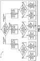
- Figure 1A is intended to provide an overview of the hardware and other operating components suitable for implementing at least certain embodiments of the invention described below, but is not intended to limit the applicable environment or any particular architecture or manner of interconnecting the components as such details are not germane to the present invention.
- PDAs personal digital assistants
- media players e.g. an iPod
- devices which combine aspects or functions of these devices (e.g.
- a media player combined with a PDA and a cellular telephone in one device an embedded processing device within another device, network computers, a peripheral device (e.g., a display device, a printer, a harddrive or other storage device, a network interface device such as a wireless router, etc.), a consumer electronic device, and other data processing systems which have fewer components or perhaps more components may also be used with or to implement one or more embodiments of the present invention.
- the data processing system of Figure 1A may, for example, be a Macintosh computer from Apple Inc.
- Figure 1A illustrates a data processing system, such as a computer system and the environment in which the embodiments of the method and system described herein may be implemented.
- the computer system 101 which is a form of a data processing system, includes a processor 103.
- Processor 103 may be configured to monitor the operative state of computer system 101 (e.g., active, low power, or standby). Although only one processor is shown, two or more microprocessors may be included in computer system 101.
- Memory 104 may be any form of memory known to those skilled in the art. Information is read from and written to mass storage 105. Mass storage 105 may be any kind of machine readable medium including, for example, magnetic media such as disk drives and magnetic tape; optical drives such as compact disk read only memory (CD-ROM) and readable and writeable compact disks (CD-RW); stick and card memory devices; ROM, RAM, flash memory devices and the like.
- Display 106 may be any display monitor known to those skilled in the art, including, for example, a cathode ray tube (CRT) display monitor and thin film transistor (TFT) display screen.
- Computer system 101 may also include an I/O controller 107, wherein input devices such as keyboard and mouse or output devices (e.g., printer, network interface device, etc.) may be coupled to the computer system 101.
- input devices such as keyboard and mouse or output devices (e.g., printer, network interface device, etc.) may be coupled to the computer system 101.
- the input devices may be any input device known to those skilled in the art and the output devices may be any output device known to those skilled in the art.
- Computer system 101 may comprise a bus 102 to facilitate connection between its various hardware components.
- Microprocessor 103, memory 104, Mass storage 105, display 106, and I/O controller 107 may be coupled to one another and communicate with one another over bus 102.
- Bus 102 may be any bus known to those skilled in the art. Although only one bus is shown, two or more buses may be included in computer system 101.
- Power can be provided to the computer system 101 by a power supply system which includes the AC input power supply 113 and the power control logic 125.
- AC input power supply 113 includes an input to receive AC mains power source 117 (e.g., 120V AC in the USA); this input provides an AC voltage to the AC-DC power converter 114 which converts (e.g., rectifies) the AC voltage (e.g. from a convention wall outlet) to a DC voltage which is applied on the voltage supply bus 110.
- the AC input power also includes a safety isolation circuit 115 and a feedback control circuit 116.
- the safety isolation circuit 115 isolates the feedback control circuit 116 (and controller 112) from the AC-DC power converter 114 so high voltage or current from the AC-DC power converter 114 do not affect the feedback control circuit 116 but allows the feedback control circuit 116 to provide a control signal, passed through the safety isolation circuit 115, to the AC-DC power converter 114 in order to adjust the DC voltage level of the DC voltage output of the AC-DC power converter 114.
- This control signal which controls the DC voltage level of the DC voltage output, is in turn controlled by an input signal received by the feedback control circuit 116 from the controller 112.
- the feedback control circuit 116 draws power from the voltage supply bus 110 as shown in Figure 1A . Two embodiments of the feedback control circuit 116 are shown in Figures 6A and 6B and are described further below in conjunction with those figures; it will be appreciated that alternative implementations of a feedback control circuit may also be used with embodiments of the invention.
- the power control logic 125 includes one or more DC to DC converter(s) 109, which provide a conversion (e.g., shift) from an input DC voltage to an output DC voltage which can be a regulated DC voltage, and an analog to digital (A/D) converter 111 and at least one controller 112.
- the DC to DC converter 109 receives its input DC voltage from the voltage supply bus 110 which is driven by the DC voltage output from the AC-DC power converter 114, and this input DC voltage is converted by the DC to DC converter 109 into the DC output voltage 121 shown as Vs which is used to provide DC power to various components in the system including microprocessor(s) 103, memory 104, mass storage 105 and controller 112.
- additional DC to DC converters may be included to provide a set of DC voltages (e.g. Vp, which may be the same as or different than Vs) to other components as shown in Figure 1A , and in certain embodiments the bidirectional connection between the controller 112 and the DC to DC converter(s) 109 can be used to control the DC to DC converter(s) 109 (e.g., to turn one or more of the converters off).
- Vp DC voltage
- the controller 112 receives power (Vs) from the DC to DC converter(s) 109, so the controller 112, the DC to DC converter(s) 109, the A/D converter 111 and the AC input power supply 113 will all be drawing power during all operative states (e.g., active power state, low power state, and standby power state) in at least certain embodiments.
- all operative states e.g., active power state, low power state, and standby power state
- This allows the system to respond to a user, even in standby power state, when the user activates a user control, such as the user control 126.
- the A/D converter 111 has an input coupled to the voltage supply bus 110 to receive the DC voltage output from the AC-DC power converter(s) 114, and the A/D converter 111 has an output, coupled to the controller 112, which provides a digital representation, of the analog DC voltage on the voltage supply bus 110 to the controller 112.
- the controller 112 may include an A/D converter and hence can provide its own A/D conversion.
- the controller 112 uses the digital representation of the analog DC voltage on the voltage supply bus 110 to monitor the DC voltage inputted to the DC to DC converter 109 and to adjust the DC voltage inputted to the DC to DC converter 109 depending on the operative state as described further in this disclosure.
- the controller 112 includes an output which provides a control signal to the feedback control 116; this control signal adjusts the feedback control 116 which in turn changes the DC voltage output from the AC-DC power converter.
- this DC voltage output By adjusting this DC voltage output, the controller 112 can change the input/output voltage ratio of the DC to DC converter 109 in order to improve efficiency (relative to a system which does not attempt to so control this input/output voltage ratio); in other words, the controller 112 can, in response to monitoring of the DC voltage output and in response to the operative state (e.g. active power state, low power state, or standby state), decrease the input/output voltage ratio (DC voltage input into the DC to DC converter divided by the DC voltage output from DC to DC converter) of the DC to DC converter.
- the operative state e.g. active power state, low power state, or standby state
- the controller 112 can decrease the DC voltage output of the AC-DC converter (which is the DC voltage input to DC to DC converter 109), while the DC voltage Vs from the DC to DC converter 109 remains substantially (typically within +/- 3%) unchanged. As long as the decrease of the DC voltage output keeps the DC voltage input to the DC to DC converter within an acceptable operating range of the DC to DC converter, then the controller 112 can improve the power efficiency of the whole system (relative to a system which does not attempt to so control the input/output voltage ratio of the DC to DC converter 109.
- the controller 112 may be a digital microcontroller which is configured to perform these operations by software (e.g. firmware) which is written to cause these operations; in other embodiments, the controller 112 may implement these operations through the use of hardware logic or a combination of hardware logic and software.
- the user controls 126 may be one or more buttons, switches, or other user interface input to the controller 112.
- the system can still respond to user input applied the user controls 126 even when the system is operating in low power state or standby state because power is supplied to the controller 112 in these states (as well as in an active power state.)
- FIG. 1B illustrates a system view of an implementation of a power supply system which can supply power to an apparatus such as a data processing system.
- the power management system 140 comprises of a power control logic 143, which comprises of a plurality of DC to DC converters, such as a system power converter 141 and a peripheral DC to DC converter 142.
- a DC to DC converter converts one DC voltage level to a second DC voltage level.
- the second DC voltage level may be a regulated DC voltage.
- the system power converter 141 provides an output DC voltage Vs which provides power to one or more components in the apparatus.
- the peripheral DC to DC to converter 143 provides power to one or more peripheral ports or devices (not shown here) such as USB hubs or ports, and may have one or more the peripheral voltage output(s) 157 (e.g.
- the analog to digital (A/D) converter 145 may be any A/D converter known to those skilled in the art that converts continuous analog signals to discrete digital signals.
- the system power converter 141, the peripheral DC to DC converter 142 and the A/D converter 145 are coupled to the voltage supply bus 144.
- a controller 147 remains active while the data processing system is in operative state and monitors the system to determine the state the apparatus is operating under (e.g., active, low power, or standby.) Controller 147 is similar to controller 112 and is coupled with the AC input power supply 149 to control the DC voltage level on the voltage supply bus 144.
- the AC input power supply 149 comprises of an AC to DC power converter 150, a feedback control 151 and a safety isolation 152; AC input power supply 149 is similar to AC input power supply 113.
- AC to DC power converter transforms AC power received from the AC mains power source 153 to DC power.
- the feedback control 151 and the safety isolation 152 are similar in function and operation to the feedback control 116 and the safety isolation 115, respectively, in Figure 1A .
- the power control logic 143 may also be coupled with user controls 154 and a host controller 155.
- the host controller 155 may also contain one or more voltage input(s) 160 to supply power to the host controller (in those embodiments in which the host controller is part of the apparatus which receives power from power management 140).
- the host controller may be in another apparatus; for example, if the apparatus receiving power from the power management system 140 is a display device (such as the display device shown in Figure 1C ), then the host controller is part of a computer (or other device with a display output to drive a display device), and this host controller drives and/or controls the driving of the display output signals to the display device.
- a display device such as the display device shown in Figure 1C
- this host controller drives and/or controls the driving of the display output signals to the display device.
- the controller 147 remains active when the system is operating.
- the controller 147 is configured to monitor the user controls 154 and the host state detection 159 to determine the operative state (e.g., active, low power, or standby) or a change in the operative state of the system.
- the controller 147 is further configured to determine the voltage level on the voltage supply bus 144. Based on the operative state of the system and the voltage level on the voltage supply bus 144, the controller 147 is configured to determine whether the voltage level on the voltage supply falls within a preset range of valid voltage level as determined the system's operative state. Typically, valid voltage levels range between, for example, 6 to 24V, depending on the system's design and operative state.
- the valid voltage level may be close to 24V when the apparatus is operating in active power state and close to 6V when the apparatus system is operating in standby state.
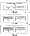
- the controller 147 determines that the voltage level on the voltage supply bus 144 is within the preset range, the system enters verified mode ( Figures 4A, 4B, and 4C ).
- verified mode the controller 147 is configured to turn on the peripheral DC to DC converter(s) 142 and the power switch(es) 146 when the system is operating in an active power state.
- the controller 147 is configured to turn on the peripheral DC to DC converter(s) 142 and turn off the power switches 146 when the system is operating in low power state.
- the controller 147 is configured to turn off the peripheral DC to DC converter(s) 142 and the power switches 146 when the system is operating in standby state. (See Figure 4C ).
- the controller 147 determines that the voltage level on the voltage supply bus 144 is not within the preset range, the system enters correction mode (See Figures 5A, 5B, and 5C ).
- the controller 147 is configured to turn off the power switch(es) 146 and the peripheral DC to DC converter(s) 142 and changes the DC output voltage of the AC input power supply 149 accordingly.
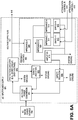
- FIG. 6A illustrates an implementation of the AC input power supply 601 (block 149 in Figure 1B ) coupled with the AC mains power source 602.
- AC input power supply 601 includes an AC to DC power conversion 603, which is similar to AC to DC converter 150, protection circuitry (e.g., short-circuit, over voltage) 604, and a safety isolation 605 and 606.
- the protection circuitry 604 is coupled with the power control logic (not shown here, block 143 of Figure 1B ) and the feedback control 607 through the voltage supply bus 617.
- the feedback control 607 comprises a plurality of impedance devices 608, 609, 611, and 612, and a plurality of switches 613 and 614.
- Feedback control 607 further comprises of amplifier 610.
- the voltage output 618 is controlled by a controller (not shown, block 147 in Figure 1B ).
- the output voltage 618 is directly related to the feedback attenuation in the AC input power supply 601.
- the controller sets the output voltage 618 at discrete levels. This may be achieved by using general purpose I/O lines on the controller 147 to drive attenuation controls 615 and 616.
- Switch 1 613 and switch N 614 can be turned on or off to increase or decrease voltage output 618.
- the DC output voltage of the AC input power system 149 in Figure 1B is adjusted linearly.
- Figure 6B illustrates an implementation of an AC input power supply 651 (block 149 in Figure 1B ).
- the AC Input power supply 651 includes an AC to DC power conversion 653, protection circuitry (e.g., short-circuit, over voltage) 654, and a safety isolation 655 and 656.
- the protection circuitry 654 is coupled with the power control logic (not shown here, block 143 in Figure 1B ) and the feedback control 657 through the voltage supply bus 667.
- the feedback control 657 comprises of impedance devices 658 and 659, an amplifier 660 and a voltage to current source 661.
- a controller (not shown, block 147 in Figure 1B ) is connected with the AC input power supply 651 to provide the attenuation control 665 as an input to the AC input power supply 651.
- the controller contains a digital to analog converter (DAC) (not shown), and uses the DAC to set the attenuation control 665, which in turn sets the DC output voltage of the AC input power supply 651 linearly.
- the controller is configured to reduce the output voltage of the DAC, which is fed into the feedback control 657. A decrease in the output voltage of the DAC will cause the voltage to current source 661 to reduce the current draw in the feedback control 657, which will cause the voltage on the voltage supply bus 617 to decrease by the attenuation control 665.
- Figure 1C shows another embodiment of the present invention.
- the power control logic 173 is further connected with a display panel 190 and one or more peripheral port(s) 187.
- the display panel 190 may comprise of a display lighting 193, a display LCD 192, and a host detection 178.
- the display lighting 193 is connected with power switches 176 which can turn the display lighting 193 (and the drivers which drive the lighting on or off).
- the display lighting 193 because the display lighting 193 receives voltage supply from the power switches 176, the display lighting 193 turns on and off when the power switches 176 are turned on or off when the system enters correction or validated mode. (See Figures 4A-C and 5A-C ).
- Figure 1C shows an example in which the apparatus, which receives power through an embodiment of the power management system of the invention is a display device.
- Figure 2 shows a generalized example of one embodiment of the present invention.
- the method of Figure 2 may begin operation in operation in 205, in which the operative state of the computer system is determined.
- the voltage level on the voltage supply bus (e.g. voltage supply bus 110, 144, 174, 618, or 668) is determined in 210.
- the voltage level on the voltage supply bus may be measured by sampling performed by the A/D converter (e.g., block 145 in Figure 1B ) several times and averaging the values to eliminate erroneous responses due to noise on the bus 210.
- the voltage level on the voltage supply bus is compared in the controller (e.g. controllers 112, 147, or 177) with a preset valid voltage range for the current power state.
- the system's current power state (e.g. active power, low power, or standby state) is known by the controller. If the voltage level determined on the voltage supply bus is within the valid voltage range, the controller causes the system to enter the verified mode for the corresponding power state in 220. If the voltage level determined on the voltage supply bus is not within the valid voltage range, the controller causes the system to enter the correction mode 215 for the corresponding power state.
- Figure 3 shows a detailed flow of actions as according to the embodiment of the method illustrated in Figure 2 (with the power management system shown in Figure 1B ).
- the method of Figure 3 may begin in operation in 305, in which the operative state of the system is determined.
- the voltage on the voltage supply bus e.g. voltage supply bus 110, 144, 174, 618, or 668 is determined.
- the voltage level on the voltage supply bus is compared with a preset valid voltage range for the current power state. If the system's operative state is active power state and the voltage level determined on the voltage supply bus is within a preset valid voltage range for active power state, the controller causes the system to enter the verified mode for active power state in 320.
- the controller causes the system to enter the correction mode for active power state in 325.
- the controller causes the system to enter verified mode for low power state 340 if the voltage level measured on the voltage bus is within a preset valid voltage range for low power state, and to enter correction mode for low power state 345 if the voltage level measured on the voltage bus is not within a preset valid voltage range for low power state.
- the controller causes the system to enter verified mode for standby power state 360 if the voltage level measured on the voltage bus is within a preset valid voltage for standby power state and correction mode for standby power state 365 if the voltage level is not within a preset valid voltage level for standby power state.
- method 301 loops back to block 305, and a new iteration of the method may be repeated.
- Figures 4A, 4B, and 4C illustrate exemplary embodiments of the present invention when the system enters the verified mode.
- verified mode for active power state 405 the peripheral power converter(s) is turned on in 410 and the power switch(es) is turned on in 415.
- verified mode for low power state 435 as shown in Figure 4B
- the peripheral power converter(s) is turned on in 440 and the power switch(es) is turned off in 445.
- verified mode for standby power state 465 as shown in Figure 4C
- the peripheral power converter(s) is turned off in 470 and the power switch(es) is turned off in 475.
- FIGS 5A, 5B, and 5C illustrate exemplary embodiments of the present invention when the system enters the correction mode.
- power converters e.g., system power converter 141 and peripheral DC to DC converter(s) 142 in Figure 1B
- the voltage supply bus voltage supply bus 144 in Figure 1B
- the controller decides if the power switches and peripheral power converters are turned off.
- the controller checks if the voltage supply bus is within the intermediate voltage range in 506.
- the intermediate voltage range is below the active power state range and above the low power state range. If the voltage supply bus is within the valid range, the peripheral power converter(s) is turned on and the power switch(es) is turned off in 508. Otherwise, the power converter(s) and power switch(es) are turned off in 510.
- the power switch(es) and peripheral power converter(s) are turned off in 540 for the excessive current draw reasons stated above and the AC input power supply feedback for low power state is adjusted in 545.
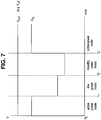
- Figure 7 is a graph of two voltages, Vout and Vin over time as a system, such as the system shown in Figures 1A or 1C , moves through different power states.
- the voltage Vout represents the DC voltage output from a DC to DC converter, such as the DC to DC converter(s) 109 in Figure 1A or the DC to DC converter 171 in Figure 1C
- the voltage Vin represents the DC input voltage which is inputted to that DC to DC converter.
- the voltage Vin is the voltage on the voltage supply bus (e.g. bus 110 in Figure 1A or bus 174 in Figure 1C ) which is controlled by a controller, such as controller 112 in Figure 1A or controller 177 in Figure 1C .
- the voltage Vout remains substantially the same over time in the different power states; it may vary slightly (for example, +/- 3%) in practice but this is considered substantially the same as the variation is within an acceptable range (of, for example, +/- 3%).
- the voltage Vin varies depending upon the operating state of the system.
- the graph in Figure 7 shows the ratio Vin/Vout in each state/mode and shows how the controller (e.g. controller 112) varies the ratio in the different states.
- the controller decreases Vin (by as much as 60%, for example, in one embodiment) while Vout remains substantially fixed; this change improves the power efficiency of the system (relative to a system which does not change the Vin/Vout ratio) as described above.
- the controller further decreases Vin (by as much as 75%, in one embodiment, relative to Vin during the active power state) to further improve the power efficiency of the system.
- the reduction of Vin also decreases the power consumption of the AC to DC converter regulation circuits, such as the protection circuitry (604 or 654 in Figures 6A or 6B ).
- the controller increases Vin back to its normal operating voltage during the active power state; this change may occur as a result of a user activating a user control or plugging in a USB Flash drive into the system or the reappearance (after a sleep or shutdown period) of a video signal being inputted into the system (in the case of the system of Figure 1C ), etc.
- the other changes occur in a typical use of the system.
- the system when in an active power mode, is normally being used by the user (e.g., the user is entering data or watching a video or reviewing a document displayed by the system).
- the system may automatically move (at time t 1 ) from the active power mode to the low power mode; in one embodiment in which the system is a display device (e.g. the system shown in Figure 1C ), the change at time t 1 may involve turning off the backlight for an LCD display (and turning off the power switches which provide the power to the backlight) while the rest of the system (e.g. the USB hub and ports) continues to receive power.
- the controller can be, in one embodiment, managing power by determining system inactivity. After a period of further inactivity (a continued period of time in which no user input has been received, the display's input has been off for an additional period of time, etc.), the system at time t 2 may, under control of the controller, move from the low power mode to the standby power mode in which only some circuits receive power (e.g. in the case of Figure 1C , only the AC input power supply, the controller 177, the A/D converter 175, the DC to DC converter 171, the user controls 184, and the Host state detection circuitry 178 receive power while the rest of the system does not receive power).
- the system at time t 2 may, under control of the controller, move from the low power mode to the standby power mode in which only some circuits receive power (e.g. in the case of Figure 1C , only the AC input power supply, the controller 177, the A/D converter 175, the DC to DC converter 171, the user controls 184, and the Host state detection
- the system while in the standby power mode can be awakened by, for example, the activation of a user control or the receipt of live display input data (e.g. the user has turned on a display driver in a computer or other apparatus); this awakening is recognized by the controller which causes the change, at time t 3 , from the standby power mode to the active power mode (in which all circuits in the system may receive power).
Landscapes
- Engineering & Computer Science (AREA)
- Power Engineering (AREA)
- Theoretical Computer Science (AREA)
- Physics & Mathematics (AREA)
- General Engineering & Computer Science (AREA)
- General Physics & Mathematics (AREA)
- Dc-Dc Converters (AREA)
- Power Sources (AREA)
- Direct Current Feeding And Distribution (AREA)
- Television Receiver Circuits (AREA)
- Rectifiers (AREA)
- Control Of Indicators Other Than Cathode Ray Tubes (AREA)
Description
- This disclosure relates generally to systems for managing power consumption, and in particular, in one embodiment, relates to systems for managing power consumption in various system states.
- Countries worldwide have adopted various programs to set standards for certifying efficient energy use of consumer products. Programs such as the Energy Star and the TCO label consumer products that are energy efficient. These programs specify levels of efficiency required for the certification of different categories of products. The programs certify products that are more efficient than a specified level of efficiency. Regarding the certification of data processing systems, the programs assess the efficiency of energy consumption based on three states of operation: active, low power, and standby.
- A data processing system operating in active state is in full operation in the system. A data processing system operating in low or standby state remains active to react to user controls or commands from a controller, but some or most of the components are turned off to reduce overall power consumption. To monitor user controls or commands, some of the circuitry of the data processing system must remain active while operating in these states. A system power converter regulates the output voltage and power level from the AC power supply. Currently, both the system power converter and the AC power supply operate at an efficiency level of 50% or less, while the data processing system is operating in low power or standby mode. Therefore, the net power efficiency level for the AC power supply and the system power converter is at 25% or less.
-
US 2004/0148531 A1 discloses a power supply system for an apparatus, the power supply system comprising: an AC to DC converter having an input to receive an AC voltage from an AC source and having a DC voltage output; a DC to DC converter having an input coupled to the DC voltage output for inputting a voltage value of the DC voltage output and having an output configured to provide a DC supply voltage to a first component of the apparatus. - The present invention relates to reducing the level of energy consumption and/or improving the level of efficiency for a data processing system that is operating in active, low energy, or standby states. While operating in these states, a controller remains active to determine which state the data processing system is operating in.
- In one aspect, system efficiency is achieved by decreasing the input voltage fed into one or more DC-to-DC converters, while maintaining the output. The efficiency of at least one power converters is inversely related to the input/output voltage ratio of the power converter. Therefore, efficiency is improved by decreasing the input voltage of a DC-to-DC converter, while maintaining the output voltage at a substantially fixed value or within a small range.
- In another aspect, system efficiency is achieved by controlling the ratio between the input and output voltage of a DC-to-DC converter(s). A controller may control the ratio between the input and output voltage of a DC to DC converter by adjusting the input voltage to the DC to DC converter while fixing the output voltage. The input voltage which is adjusted can be the DC output voltage from an AC to DC converter, which is controlled by the controller which receives power from the DC to DC converters.
- The present invention provides a power supply system for an apparatus according to
claim 1 and a corresponding method for operating a power supply for an apparatus according toclaim 11. Preferred embodiments are defined in the dependent claims. - The present invention is illustrated by way of example and not limitation in the figures of the accompanying drawings in which like references indicate similar elements.
-
Figure 1A illustrates a data processing system, such as a computer system, and the environment in which at least certain of the embodiments of the method and system described herein may be implemented. -
Figure 1B illustrates an embodiment of a power management system which can be used to manage power consumption of an apparatus receiving power from the power management system according to at least certain embodiments described herein. -
Figure 1C illustrates an embodiment of a display device according to certain aspects of the present invention. -
Figure 2 illustrates the flow of actions taken according to an embodiment of a method to improve power efficiency of a data processing system. -
Figure 3 illustrates a flow chart of actions according to the embodiment of a method as illustrated inFigure 2 . -
Figure 4A illustrates a flow chart of an embodiment of a method when a data processing system enters verified mode for active power state. -
Figure 4B illustrates a flow chart of an embodiment of a method when a data processing system enters verified mode for low power state. -
Figure 4C illustrates a flow chart of an embodiment of a method when a data processing system enters verified mode for standby power state. -
Figure 5A illustrates the flow of actions taken according to an embodiment of method when a computer system enters correction mode for active power state. -
Figure 5B illustrates the flow of actions taken according to an embodiment of a method when a computer system enters correction mode for low power state. -
Figure 5C illustrates the flow of actions taken according to an embodiment of a method when a computer system enters correction mode for standby power state. -
Figure 6A illustrates an AC input power supply unit according to one embodiment of the present invention. -
Figure 6B illustrates an AC input power supply unit according to another embodiment of the present invention. -
Figure 7 shows a graph of two voltages (Vout and Vin) over time. - Various embodiments and aspects of the inventions will be described with reference to details discussed below, and the accompanying drawings will illustrate the various embodiments. The following description and drawings are illustrative of the invention and are not to be construed as limiting the invention. Numerous specific details are described to provide a thorough understanding of various embodiments of the present invention. However, in certain instances, well-known or conventional details are not described in order to provide a concise discussion of embodiments of the present inventions.
- Reference in the specification to one embodiment or an embodiment means that a particular feature, structure, or characteristic described in connection with the embodiment is included in at least one embodiment of the invention. The appearance of the phrase "in one embodiment" in various places in the specification do not necessarily refer to the same embodiment.
- The invention described herein provides various embodiments of a method and system for reducing the level of energy consumption and for improving the level of efficiency for a data processing system. As many data operating systems operate at an efficiency level of less than 25% when the device is in low and standby power state, the various embodiments of the system and method described herein may be implemented as part of the data processing system to improve the consumption rate to reach a predetermined level of efficiency. The various embodiments of the system and method described herein may be incorporated as part of a data processing system.
- The following description of
Figure 1A is intended to provide an overview of the hardware and other operating components suitable for implementing at least certain embodiments of the invention described below, but is not intended to limit the applicable environment or any particular architecture or manner of interconnecting the components as such details are not germane to the present invention. One of skill in the art will appreciate that the invention can be practiced with other data processing configurations, including hand-held devices, cellular telephones, multiprocessor systems, microprocessor-based or programmable consumer electronics/appliances, and network PCs, minicomputers, mainframe computers, and the like. It will also be appreciated that personal digital assistants (PDAs), media players (e.g. an iPod), devices which combine aspects or functions of these devices (e.g. a media player combined with a PDA and a cellular telephone in one device), an embedded processing device within another device, network computers, a peripheral device (e.g., a display device, a printer, a harddrive or other storage device, a network interface device such as a wireless router, etc.), a consumer electronic device, and other data processing systems which have fewer components or perhaps more components may also be used with or to implement one or more embodiments of the present invention. The data processing system ofFigure 1A may, for example, be a Macintosh computer from Apple Inc. -
Figure 1A illustrates a data processing system, such as a computer system and the environment in which the embodiments of the method and system described herein may be implemented. - As shown in
Figure 1A , thecomputer system 101, which is a form of a data processing system, includes aprocessor 103.Processor 103 may be configured to monitor the operative state of computer system 101 (e.g., active, low power, or standby). Although only one processor is shown, two or more microprocessors may be included incomputer system 101.Memory 104 may be any form of memory known to those skilled in the art. Information is read from and written tomass storage 105.Mass storage 105 may be any kind of machine readable medium including, for example, magnetic media such as disk drives and magnetic tape; optical drives such as compact disk read only memory (CD-ROM) and readable and writeable compact disks (CD-RW); stick and card memory devices; ROM, RAM, flash memory devices and the like.Display 106 may be any display monitor known to those skilled in the art, including, for example, a cathode ray tube (CRT) display monitor and thin film transistor (TFT) display screen.Computer system 101 may also include an I/O controller 107, wherein input devices such as keyboard and mouse or output devices (e.g., printer, network interface device, etc.) may be coupled to thecomputer system 101. The input devices may be any input device known to those skilled in the art and the output devices may be any output device known to those skilled in the art. -
Computer system 101 may comprise a bus 102 to facilitate connection between its various hardware components.Microprocessor 103,memory 104,Mass storage 105,display 106, and I/O controller 107 may be coupled to one another and communicate with one another over bus 102. Bus 102 may be any bus known to those skilled in the art. Although only one bus is shown, two or more buses may be included incomputer system 101. - Power can be provided to the
computer system 101 by a power supply system which includes the ACinput power supply 113 and thepower control logic 125. ACinput power supply 113 includes an input to receive AC mains power source 117 (e.g., 120V AC in the USA); this input provides an AC voltage to the AC-DC power converter 114 which converts (e.g., rectifies) the AC voltage (e.g. from a convention wall outlet) to a DC voltage which is applied on the voltage supply bus 110. The AC input power also includes asafety isolation circuit 115 and afeedback control circuit 116. Thesafety isolation circuit 115 isolates the feedback control circuit 116 (and controller 112) from the AC-DC power converter 114 so high voltage or current from the AC-DC power converter 114 do not affect thefeedback control circuit 116 but allows thefeedback control circuit 116 to provide a control signal, passed through thesafety isolation circuit 115, to the AC-DC power converter 114 in order to adjust the DC voltage level of the DC voltage output of the AC-DC power converter 114. This control signal, which controls the DC voltage level of the DC voltage output, is in turn controlled by an input signal received by thefeedback control circuit 116 from thecontroller 112. Thefeedback control circuit 116 draws power from the voltage supply bus 110 as shown inFigure 1A . Two embodiments of thefeedback control circuit 116 are shown inFigures 6A and6B and are described further below in conjunction with those figures; it will be appreciated that alternative implementations of a feedback control circuit may also be used with embodiments of the invention. - The
power control logic 125 includes one or more DC to DC converter(s) 109, which provide a conversion (e.g., shift) from an input DC voltage to an output DC voltage which can be a regulated DC voltage, and an analog to digital (A/D)converter 111 and at least onecontroller 112. The DC toDC converter 109 receives its input DC voltage from the voltage supply bus 110 which is driven by the DC voltage output from the AC-DC power converter 114, and this input DC voltage is converted by the DC toDC converter 109 into theDC output voltage 121 shown as Vs which is used to provide DC power to various components in the system including microprocessor(s) 103,memory 104,mass storage 105 andcontroller 112. In certain embodiments, additional DC to DC converters may be included to provide a set of DC voltages (e.g. Vp, which may be the same as or different than Vs) to other components as shown inFigure 1A , and in certain embodiments the bidirectional connection between thecontroller 112 and the DC to DC converter(s) 109 can be used to control the DC to DC converter(s) 109 (e.g., to turn one or more of the converters off). In the example shown inFigure 1A , thecontroller 112 receives power (Vs) from the DC to DC converter(s) 109, so thecontroller 112, the DC to DC converter(s) 109, the A/D converter 111 and the ACinput power supply 113 will all be drawing power during all operative states (e.g., active power state, low power state, and standby power state) in at least certain embodiments. This allows the system to respond to a user, even in standby power state, when the user activates a user control, such as the user control 126. The A/D converter 111 has an input coupled to the voltage supply bus 110 to receive the DC voltage output from the AC-DC power converter(s) 114, and the A/D converter 111 has an output, coupled to thecontroller 112, which provides a digital representation, of the analog DC voltage on the voltage supply bus 110 to thecontroller 112. In an alternative embodiment, thecontroller 112 may include an A/D converter and hence can provide its own A/D conversion. Thecontroller 112 uses the digital representation of the analog DC voltage on the voltage supply bus 110 to monitor the DC voltage inputted to the DC toDC converter 109 and to adjust the DC voltage inputted to the DC toDC converter 109 depending on the operative state as described further in this disclosure. Thecontroller 112 includes an output which provides a control signal to thefeedback control 116; this control signal adjusts thefeedback control 116 which in turn changes the DC voltage output from the AC-DC power converter. By adjusting this DC voltage output, thecontroller 112 can change the input/output voltage ratio of the DC toDC converter 109 in order to improve efficiency (relative to a system which does not attempt to so control this input/output voltage ratio); in other words, thecontroller 112 can, in response to monitoring of the DC voltage output and in response to the operative state (e.g. active power state, low power state, or standby state), decrease the input/output voltage ratio (DC voltage input into the DC to DC converter divided by the DC voltage output from DC to DC converter) of the DC to DC converter. In the standby state, thecontroller 112 can decrease the DC voltage output of the AC-DC converter (which is the DC voltage input to DC to DC converter 109), while the DC voltage Vs from the DC toDC converter 109 remains substantially (typically within +/- 3%) unchanged. As long as the decrease of the DC voltage output keeps the DC voltage input to the DC to DC converter within an acceptable operating range of the DC to DC converter, then thecontroller 112 can improve the power efficiency of the whole system (relative to a system which does not attempt to so control the input/output voltage ratio of the DC toDC converter 109. Thecontroller 112 may be a digital microcontroller which is configured to perform these operations by software (e.g. firmware) which is written to cause these operations; in other embodiments, thecontroller 112 may implement these operations through the use of hardware logic or a combination of hardware logic and software. - The user controls 126 may be one or more buttons, switches, or other user interface input to the
controller 112. The system can still respond to user input applied the user controls 126 even when the system is operating in low power state or standby state because power is supplied to thecontroller 112 in these states (as well as in an active power state.) -
Figure 1B illustrates a system view of an implementation of a power supply system which can supply power to an apparatus such as a data processing system. Thepower management system 140 comprises of apower control logic 143, which comprises of a plurality of DC to DC converters, such as asystem power converter 141 and a peripheral DC toDC converter 142. A DC to DC converter converts one DC voltage level to a second DC voltage level. The second DC voltage level may be a regulated DC voltage. Thesystem power converter 141 provides an output DC voltage Vs which provides power to one or more components in the apparatus. The peripheral DC to DC toconverter 143 provides power to one or more peripheral ports or devices (not shown here) such as USB hubs or ports, and may have one or more the peripheral voltage output(s) 157 (e.g. Vp) coupled to it. The analog to digital (A/D)converter 145 may be any A/D converter known to those skilled in the art that converts continuous analog signals to discrete digital signals. Thesystem power converter 141, the peripheral DC toDC converter 142 and the A/D converter 145 are coupled to thevoltage supply bus 144. Acontroller 147 remains active while the data processing system is in operative state and monitors the system to determine the state the apparatus is operating under (e.g., active, low power, or standby.)Controller 147 is similar tocontroller 112 and is coupled with the ACinput power supply 149 to control the DC voltage level on thevoltage supply bus 144. The ACinput power supply 149 comprises of an AC toDC power converter 150, afeedback control 151 and asafety isolation 152; ACinput power supply 149 is similar to AC inputpower supply 113. AC to DC power converter transforms AC power received from the ACmains power source 153 to DC power. Thefeedback control 151 and thesafety isolation 152 are similar in function and operation to thefeedback control 116 and thesafety isolation 115, respectively, inFigure 1A . Thepower control logic 143 may also be coupled with user controls 154 and ahost controller 155. Thehost controller 155 may also contain one or more voltage input(s) 160 to supply power to the host controller (in those embodiments in which the host controller is part of the apparatus which receives power from power management 140). In certain embodiments, the host controller may be in another apparatus; for example, if the apparatus receiving power from thepower management system 140 is a display device (such as the display device shown inFigure 1C ), then the host controller is part of a computer (or other device with a display output to drive a display device), and this host controller drives and/or controls the driving of the display output signals to the display device. - In one embodiment, the
controller 147 remains active when the system is operating. Thecontroller 147 is configured to monitor the user controls 154 and thehost state detection 159 to determine the operative state (e.g., active, low power, or standby) or a change in the operative state of the system. Thecontroller 147 is further configured to determine the voltage level on thevoltage supply bus 144. Based on the operative state of the system and the voltage level on thevoltage supply bus 144, thecontroller 147 is configured to determine whether the voltage level on the voltage supply falls within a preset range of valid voltage level as determined the system's operative state. Typically, valid voltage levels range between, for example, 6 to 24V, depending on the system's design and operative state. The valid voltage level may be close to 24V when the apparatus is operating in active power state and close to 6V when the apparatus system is operating in standby state. If thecontroller 147 determines that the voltage level on thevoltage supply bus 144 is within the preset range, the system enters verified mode (Figures 4A, 4B, and 4C ). In verified mode, thecontroller 147 is configured to turn on the peripheral DC to DC converter(s) 142 and the power switch(es) 146 when the system is operating in an active power state. (SeeFigure 4A ). Thecontroller 147 is configured to turn on the peripheral DC to DC converter(s) 142 and turn off the power switches 146 when the system is operating in low power state. (SeeFigure 4B ). Thecontroller 147 is configured to turn off the peripheral DC to DC converter(s) 142 and the power switches 146 when the system is operating in standby state. (SeeFigure 4C ). - On the other hand, if the
controller 147 determines that the voltage level on thevoltage supply bus 144 is not within the preset range, the system enters correction mode (SeeFigures 5A, 5B, and 5C ). When a system is in correction mode, thecontroller 147 is configured to turn off the power switch(es) 146 and the peripheral DC to DC converter(s) 142 and changes the DC output voltage of the ACinput power supply 149 accordingly. - When the computer system is in an operative state, power converters that are coupled with the voltage supply bus 144 (e.g.,
system power converter 141 and peripheral DC to DC converter(s) 142.) draw constant power fromvoltage supply bus 144. Therefore, when thecontroller 147 decreases the output voltage of thefeedback control 151, which results in a decrease in the input voltage of the DC to DC converters coupled with thesystem voltage bus 144, the input current of the DC to DC converters increases to maintain constant power. To avoid excessive current draw by the DC to DC converters, thecontroller 147 shuts down power switch(es) 146 and peripheral DC to DC converter(s) 142 before adjusting the DC output voltage of the ACinput power supply 149 to transition to standby power state. To prevent excessive current draw, thecontroller 147 shuts down power switch(es) 146 before adjusting the DC output voltage of the ACinput power supply 149 to transition to low power state. - In one embodiment, the output signal from the
feedback control 151 is adjusted by a feedback attenuation signal from thecontroller 147.Figure 6A illustrates an implementation of the AC input power supply 601 (block 149 inFigure 1B ) coupled with the ACmains power source 602. ACinput power supply 601 includes an AC toDC power conversion 603, which is similar to AC toDC converter 150, protection circuitry (e.g., short-circuit, over voltage) 604, and asafety isolation protection circuitry 604 is coupled with the power control logic (not shown here, block 143 ofFigure 1B ) and thefeedback control 607 through the voltage supply bus 617. Thefeedback control 607 comprises a plurality ofimpedance devices switches Feedback control 607 further comprises ofamplifier 610. - In one embodiment, the
voltage output 618 is controlled by a controller (not shown, block 147 inFigure 1B ). In one implementation, theoutput voltage 618 is directly related to the feedback attenuation in the ACinput power supply 601. To decrease theoutput voltage 618, the controller sets theoutput voltage 618 at discrete levels. This may be achieved by using general purpose I/O lines on thecontroller 147 to drive attenuation controls 615 and 616.Switch 1 613 and switchN 614 can be turned on or off to increase or decreasevoltage output 618. - In another embodiment, the DC output voltage of the AC
input power system 149 inFigure 1B is adjusted linearly.Figure 6B illustrates an implementation of an AC input power supply 651 (block 149 inFigure 1B ). In this implementation, the ACInput power supply 651 includes an AC toDC power conversion 653, protection circuitry (e.g., short-circuit, over voltage) 654, and asafety isolation protection circuitry 654 is coupled with the power control logic (not shown here, block 143 inFigure 1B ) and thefeedback control 657 through the voltage supply bus 667. Thefeedback control 657 comprises ofimpedance devices amplifier 660 and a voltage tocurrent source 661. - In one embodiment, a controller (not shown, block 147 in
Figure 1B ) is connected with the ACinput power supply 651 to provide theattenuation control 665 as an input to the ACinput power supply 651. The controller contains a digital to analog converter (DAC) (not shown), and uses the DAC to set theattenuation control 665, which in turn sets the DC output voltage of the ACinput power supply 651 linearly. In one implementation, the controller is configured to reduce the output voltage of the DAC, which is fed into thefeedback control 657. A decrease in the output voltage of the DAC will cause the voltage tocurrent source 661 to reduce the current draw in thefeedback control 657, which will cause the voltage on the voltage supply bus 617 to decrease by theattenuation control 665. -
Figure 1C shows another embodiment of the present invention. In this implementation, thepower control logic 173 is further connected with adisplay panel 190 and one or more peripheral port(s) 187. Thedisplay panel 190 may comprise of adisplay lighting 193, adisplay LCD 192, and ahost detection 178. Thedisplay lighting 193 is connected withpower switches 176 which can turn the display lighting 193 (and the drivers which drive the lighting on or off). In this embodiment, because thedisplay lighting 193 receives voltage supply from the power switches 176, thedisplay lighting 193 turns on and off when the power switches 176 are turned on or off when the system enters correction or validated mode. (SeeFigures 4A-C and5A-C ).Figure 1C shows an example in which the apparatus, which receives power through an embodiment of the power management system of the invention is a display device. -
Figure 2 shows a generalized example of one embodiment of the present invention. The method ofFigure 2 may begin operation in operation in 205, in which the operative state of the computer system is determined. The voltage level on the voltage supply bus (e.g.voltage supply bus Figure 1B ) several times and averaging the values to eliminate erroneous responses due to noise on the bus 210. The voltage level on the voltage supply bus is compared in the controller (e.g. controllers correction mode 215 for the corresponding power state. -
Figure 3 shows a detailed flow of actions as according to the embodiment of the method illustrated inFigure 2 (with the power management system shown inFigure 1B ). The method ofFigure 3 may begin in operation in 305, in which the operative state of the system is determined. In 310, 330, and 350, the voltage on the voltage supply bus (e.g.voltage supply bus low power state 340 if the voltage level measured on the voltage bus is within a preset valid voltage range for low power state, and to enter correction mode forlow power state 345 if the voltage level measured on the voltage bus is not within a preset valid voltage range for low power state. Lastly, the controller causes the system to enter verified mode for standby power state 360 if the voltage level measured on the voltage bus is within a preset valid voltage for standby power state and correction mode forstandby power state 365 if the voltage level is not within a preset valid voltage level for standby power state. After the computer undergoes the respective verified or correction mode for the operative state of the computer system,method 301 loops back to block 305, and a new iteration of the method may be repeated. -
Figures 4A, 4B, and 4C illustrate exemplary embodiments of the present invention when the system enters the verified mode. In verified mode foractive power state 405, as shown inFigure 4A , the peripheral power converter(s) is turned on in 410 and the power switch(es) is turned on in 415. In verified mode forlow power state 435, as shown inFigure 4B , the peripheral power converter(s) is turned on in 440 and the power switch(es) is turned off in 445. Lastly, in verified mode forstandby power state 465, as shown inFigure 4C , the peripheral power converter(s) is turned off in 470 and the power switch(es) is turned off in 475. -
Figures 5A, 5B, and 5C illustrate exemplary embodiments of the present invention when the system enters the correction mode. When the system is in active operative mode, power converters (e.g.,system power converter 141 and peripheral DC to DC converter(s) 142 inFigure 1B ) coupled with the voltage supply bus (voltage supply bus 144 inFigure 1B ) draw constant power. When the input voltage that is fed into these converters decreases because the power supply feedback for active power state is adjusted in 515, the input current that is fed into the power converters increases to maintain constant power. To avoid the excessive current draw, the controller decides if the power switches and peripheral power converters are turned off. In correction mode foractive power state 505, as shown inFigure 5A , the controller checks if the voltage supply bus is within the intermediate voltage range in 506. The intermediate voltage range is below the active power state range and above the low power state range. If the voltage supply bus is within the valid range, the peripheral power converter(s) is turned on and the power switch(es) is turned off in 508. Otherwise, the power converter(s) and power switch(es) are turned off in 510. In correction mode forlow power state 530, as shown inFigure 5B , the power switch(es) and peripheral power converter(s) are turned off in 540 for the excessive current draw reasons stated above and the AC input power supply feedback for low power state is adjusted in 545. In correction mode forstandby power state 560, as shown inFigure 5C , the power switch(es) and peripheral power converter(s) are turned off in 570 for the excessive current draw reasons stated above and the AC input power supply feedback for active power state is adjusted in 575. -
Figure 7 is a graph of two voltages, Vout and Vin over time as a system, such as the system shown inFigures 1A or1C , moves through different power states. The voltage Vout represents the DC voltage output from a DC to DC converter, such as the DC to DC converter(s) 109 inFigure 1A or the DC toDC converter 171 inFigure 1C , and the voltage Vin represents the DC input voltage which is inputted to that DC to DC converter. The voltage Vin is the voltage on the voltage supply bus (e.g. bus 110 inFigure 1A orbus 174 inFigure 1C ) which is controlled by a controller, such ascontroller 112 inFigure 1A orcontroller 177 inFigure 1C . The voltage Vout remains substantially the same over time in the different power states; it may vary slightly (for example, +/- 3%) in practice but this is considered substantially the same as the variation is within an acceptable range (of, for example, +/- 3%). On the other hand, the voltage Vin varies depending upon the operating state of the system. The graph inFigure 7 shows the ratio Vin/Vout in each state/mode and shows how the controller (e.g. controller 112) varies the ratio in the different states. In particular, in the change from the active power state (during period t0 to t1) to the low power state (during period t1 to t2), the controller decreases Vin (by as much as 60%, for example, in one embodiment) while Vout remains substantially fixed; this change improves the power efficiency of the system (relative to a system which does not change the Vin/Vout ratio) as described above. In the change from the low power state, which exists from t1 to t2, to the standby state (which exists during period t2 to t3), the controller further decreases Vin (by as much as 75%, in one embodiment, relative to Vin during the active power state) to further improve the power efficiency of the system. The reduction of Vin also decreases the power consumption of the AC to DC converter regulation circuits, such as the protection circuitry (604 or 654 inFigures 6A or6B ). In the change from the standby power state, which exists during time t2 to t3, to the active power state, the controller increases Vin back to its normal operating voltage during the active power state; this change may occur as a result of a user activating a user control or plugging in a USB Flash drive into the system or the reappearance (after a sleep or shutdown period) of a video signal being inputted into the system (in the case of the system ofFigure 1C ), etc. The other changes occur in a typical use of the system. For example, the system, when in an active power mode, is normally being used by the user (e.g., the user is entering data or watching a video or reviewing a document displayed by the system). After a period of inactivity (no user input for over X minutes, the input display has not changed for X minutes, etc.), the system may automatically move (at time t1) from the active power mode to the low power mode; in one embodiment in which the system is a display device (e.g. the system shown inFigure 1C ), the change at time t1 may involve turning off the backlight for an LCD display (and turning off the power switches which provide the power to the backlight) while the rest of the system (e.g. the USB hub and ports) continues to receive power. The controller can be, in one embodiment, managing power by determining system inactivity. After a period of further inactivity (a continued period of time in which no user input has been received, the display's input has been off for an additional period of time, etc.), the system at time t2 may, under control of the controller, move from the low power mode to the standby power mode in which only some circuits receive power (e.g. in the case ofFigure 1C , only the AC input power supply, thecontroller 177, the A/D converter 175, the DC toDC converter 171, the user controls 184, and the Hoststate detection circuitry 178 receive power while the rest of the system does not receive power). The system, while in the standby power mode can be awakened by, for example, the activation of a user control or the receipt of live display input data (e.g. the user has turned on a display driver in a computer or other apparatus); this awakening is recognized by the controller which causes the change, at time t3, from the standby power mode to the active power mode (in which all circuits in the system may receive power). - The scope of the invention is to be determined entirely by the following claims.
Claims (20)
- A power supply system for an apparatus, the power supply system comprising:an AC (alternating current) to DC (direct current) converter (114,150,180) having an input to receive an AC voltage from an AC source (117,153,183) and having a DC voltage output and having a control input, the control input being configured to control a voltage (Vin) of the DC voltage output;a DC to DC converter (109,141,171) having an input coupled to the DC voltage output for inputting a voltage value (Vin) of the DC voltage output and having an output configured to provide a DC supply voltage (Vs,Vout,121,156,186) to a first component of the apparatus, the DC to DC converter being a step-up converter to maintain a substantially fixed voltage value of the DC supply voltage when the voltage value of the DC voltage output changes; anda controller (112,147,177) having a first input coupled to the DC voltage output and having an output coupled to the control input of the AC to DC converter, the controller being configured to adjust the voltage of the DC voltage output in accordance with an operating state of the apparatus detected by the power supply system for the apparatus, wherein when the operating state changes between different power modes, the controller adjusts the output of the controller to cause the AC to DC converter to change the voltage of the DC voltage output to a value within a valid range for the power mode, and wherein the voltage of the DC voltage output remains unchanged until the change of the operating state between the different power modes.
- The power supply system of claim 1 wherein the DC supply voltage of the DC to DC converter provides power to the controller.
- The power supply system of claim 1, further comprising an analog to digital (A/D) converter configured to convert an analog voltage value to a digital value representing the analog voltage value to allow the controller to monitor the voltage of the DC voltage output, and wherein the controller is coupled to the DC voltage output through the A/D converter.
- The power supply system of claim 3, wherein the A/D converter has an input coupled to the DC voltage output of the AC to DC converter and has an output coupled to the first input of the controller.
- The power supply system of claim 1, wherein the controller holds the voltage of the DC voltage output within an operating range of an input DC voltage at the input of the DC to DC converter.
- The power supply system of claim 1 wherein the power modes comprise an active power mode, and at least one of a low power mode and a standby power mode.
- The power supply system of claim 6 wherein reducing the voltage of the DC voltage output lowers power consumed by the apparatus during the standby mode.
- The power supply system of claim 6 further comprising:
a host controller (155,185) for driving and/or controlling the driving of output signals to a display device coupled to the apparatus, wherein the controller is connected to the host controller to change the operating state from the standby power mode to the active power mode when the controller detects that live display input data is received from the output of the host controller under the standby power mode. - The power supply system of claim 6, wherein when the operating state changes from the low power mode to the standby power mode, the controller turns off the DC to DC converter and when the operating state changes from the standby power mode to the active power mode, the controller turns on the DC to DC converter.
- The power supply system of claim 6, wherein when the operating state changes from the active power mode to the low power mode, the controller adjusts the output of the controller to reduce the voltage of the DC voltage output to a second value that is lower than a first value for the active power mode, when the operating state changes from the low voltage mode to a standby mode, the controller adjusts the output of the controller to reduce the voltage of the DC voltage output to a third value that is lower than the second value, and when the operating state changes from the standby power mode to the active power mode, the controller adjusts the output of the controller to increase the voltage of the DC voltage output from the third value to the first value.
- A method for operating a power supply for an apparatus, the power supply including an AC (alternating current) to DC (direct current) converter (114,150,180) having an input to receive an AC voltage from an AC source (117,153,183), J having a DC voltage output and having a control configured to control a voltage (Vin) of the DC voltage output, a DC to DC step-up converter (109,141,171) having an input coupled to the DC voltage output for inputting a voltage value (Vin) of the DC voltage output and having an output configured to provide a DC supply voltage (Vs,Vout,121,156,186) to a first component of the apparatus, the DC to DC step-up converter maintaining a substantially fixed voltage value of the DC supply voltage when the voltage value of the DC voltage output changes, and a controller having a first input coupled to the voltage of the DC voltage output of the AC to DC converter and having an output coupled to the control input of the AC to DC converter, the method comprising:monitoring, by the controller, an operating state of the apparatus detected by the power supply for the apparatus; andin response to detecting a change in the operating state between power modes, adjusting, by the controller, the voltage to change the voltage of the DC voltage output to a value within a valid range for the power mode, wherein the voltage of the DC voltage output remains unchanged until the change of the operating state between the different power modes.
- The method of claim 11, wherein the DC supply voltage of the DC to DC converter provides power to the controller.
- The method of claim 11, wherein the power supply further comprises an analog to digital (A/D) converter configured to convert an analog voltage value to a digital value representing the analog voltage value to allow the controller to monitor the voltage of the DC voltage output, and wherein the controller is coupled to the DC voltage output through the A/D converter.
- The method of claim 13, wherein the A/D converter has an input coupled to the DC voltage output of the AC to DC converter and has an output coupled to the first input of the controller.
- The method of claim 11, wherein the controller holds the voltage of the DC voltage output within an operating range of an input DC voltage at the input of the DC to DC converter.
- The method of claim 11, wherein the power modes comprise an active power mode, and at least one of a low power mode and a standby power mode.
- The method of claim 16, wherein reducing the voltage of the DC voltage output lowers power consumed by the apparatus during the standby power mode.
- The method of claim 16, wherein the power supply further comprises a host controller for driving and/or controlling the driving of display output signals to a display device coupled to the apparatus, wherein the controller is connected to the host controller to change the operating state from the standby power mode to the active power mode when the controller detects that live display input data is received from the output of the host controller under the standby power mode.
- The method of claim 16, wherein when the operating state changes from the low power mode to the standby power mode, the controller turns off the DC to DC converter and when the operating state changes from the standby power mode to the active power mode, the controller turns on the DC to DC converter.
- The method of claim 16, wherein when the operating state changes from the active power mode to the low power mode, the controller adjusts the output of the controller to reduce the voltage of the DC voltage output to a second value that is lower than a first value for the active power mode, when the operating state changes from the low voltage mode to a standby mode, the controller adjusts the output of the controller to reduce the voltage of the DC voltage output to a third value that is lower than the second value, and when the operating state changes from the standby power mode to the active power mode, the controller adjusts the output of the controller to increase the voltage of the DC voltage output from the third value to the first value.
Applications Claiming Priority (2)
| Application Number | Priority Date | Filing Date | Title |
|---|---|---|---|
| US12/250,522 US8599589B2 (en) | 2008-10-13 | 2008-10-13 | Methods and systems for reducing power consumption |
| PCT/US2009/060255 WO2010045126A1 (en) | 2008-10-13 | 2009-10-09 | Reducing power consumption in an ac powered data processing or display device |
Publications (2)
| Publication Number | Publication Date |
|---|---|
| EP2335345A1 EP2335345A1 (en) | 2011-06-22 |
| EP2335345B1 true EP2335345B1 (en) | 2019-01-02 |
Family
ID=41571298
Family Applications (1)
| Application Number | Title | Priority Date | Filing Date |
|---|---|---|---|
| EP09741096.3A Active EP2335345B1 (en) | 2008-10-13 | 2009-10-09 | Reducing power consumption in an ac powered data processing or display device |
Country Status (9)
| Country | Link |
|---|---|
| US (1) | US8599589B2 (en) |
| EP (1) | EP2335345B1 (en) |
| JP (2) | JP2012505631A (en) |
| KR (1) | KR101233513B1 (en) |
| CN (1) | CN102224666B (en) |
| GB (1) | GB2476430B (en) |
| HK (1) | HK1163382A1 (en) |
| TW (1) | TWI410790B (en) |
| WO (1) | WO2010045126A1 (en) |
Families Citing this family (29)
| Publication number | Priority date | Publication date | Assignee | Title |
|---|---|---|---|---|
| KR101264805B1 (en) * | 2008-11-20 | 2013-05-15 | 삼성전자주식회사 | Method and System for providing presence service |
| US8134848B2 (en) * | 2009-08-12 | 2012-03-13 | Alcatel Lucent | Closed-loop efficiency modulation for use in AC powered applications |
| US9130400B2 (en) * | 2009-09-24 | 2015-09-08 | Apple Inc. | Multiport power converter with load detection capabilities |
| US8896157B2 (en) * | 2009-11-24 | 2014-11-25 | Delta Electronics, Inc. | Power supply and power supplying system with remote power management function |
| WO2013012411A1 (en) * | 2011-07-18 | 2013-01-24 | Hewlett-Packard Development Company, L.P. | Power consumption limit associated with power over ethernet (poe) computing system |
| JP5915092B2 (en) * | 2011-11-02 | 2016-05-11 | 富士ゼロックス株式会社 | Information processing apparatus, information processing system, and information processing program |
| US9839967B2 (en) * | 2011-11-08 | 2017-12-12 | Lincoln Global, Inc. | System and method for real-time computation and reporting of welding machine performance and metrics |
| JP5829903B2 (en) * | 2011-12-22 | 2015-12-09 | ミネベア株式会社 | Power supply system, switching power supply apparatus, control parameter generation apparatus, and program |
| US20130197895A1 (en) * | 2012-01-31 | 2013-08-01 | Zhikui Wang | Real-time server management |
| JP2014021598A (en) * | 2012-07-13 | 2014-02-03 | Funai Electric Co Ltd | Electronic device, and video system |
| US20150048782A1 (en) * | 2013-08-17 | 2015-02-19 | Trevor Jason Back | Electric Power Supply Adapter Device for Club Car Golf Cars and Utility Vehicles |
| KR102300316B1 (en) * | 2014-03-06 | 2021-09-10 | 삼성디스플레이 주식회사 | Stand-by power controlling device, liquid crystal display device including the same, and method of controlling stand-by power |
| JP2015171289A (en) * | 2014-03-10 | 2015-09-28 | コニカミノルタ株式会社 | Power supply controller |
| TWI503645B (en) * | 2014-05-07 | 2015-10-11 | Nuvoton Technology Corp | Voltage regulator and voltage regulating method and chip using the same |
| US9621070B2 (en) * | 2014-09-17 | 2017-04-11 | Delta Electronics, Inc. | Power supply with multiple converters and averaged feedforward control |
| JP6107774B2 (en) | 2014-09-18 | 2017-04-05 | コニカミノルタ株式会社 | Power supply control apparatus, image forming apparatus, power supply control apparatus control method, and power supply control apparatus control program |
| US10545907B2 (en) | 2015-12-24 | 2020-01-28 | Intel Corporation | Adjustable power delivery scheme for universal serial bus |
| US20170187219A1 (en) * | 2015-12-24 | 2017-06-29 | Intel Corporation | Wireless charging system |
| US10481661B2 (en) | 2016-03-30 | 2019-11-19 | Intel Corporation | Power supply interface light load signal |
| KR101657593B1 (en) * | 2016-05-18 | 2016-09-19 | (주)이엠텍아이엔씨 | A method for monitoring the operating state of a computer system, and the power saving method utilizing the same |
| US10310038B2 (en) | 2016-05-24 | 2019-06-04 | General Electric Company | System and method for supplying electrical power to a gradient amplifier |
| WO2019212525A1 (en) | 2018-04-30 | 2019-11-07 | Hewlett-Packard Development Company, L.P. | Isolating electrical components |
| US11379030B2 (en) | 2018-05-01 | 2022-07-05 | Lenovo (Singapore) Pte. Ltd. | Controlling power efficiency of an information processing device |
| JP2019194762A (en) * | 2018-05-01 | 2019-11-07 | レノボ・シンガポール・プライベート・リミテッド | Information processing device and control method |
| CN108767840A (en) * | 2018-07-26 | 2018-11-06 | 深圳供电局有限公司 | Power supply and utilization equipment behavior management system and method |
| TWI683198B (en) | 2018-09-14 | 2020-01-21 | 威鋒電子股份有限公司 | Multi-port power supply apparatus and power suppling method thereof |
| US10983852B2 (en) | 2019-01-30 | 2021-04-20 | Micron Technology, Inc. | Power management component for memory sub-system voltage regulation |
| CN110289662B (en) * | 2019-02-13 | 2021-09-21 | 威锋电子股份有限公司 | Multi-port power supply device and operation method thereof |
| CN111711263B (en) * | 2020-06-29 | 2024-02-09 | 王军库 | Monitor power supply switching system |
Citations (1)
| Publication number | Priority date | Publication date | Assignee | Title |
|---|---|---|---|---|
| US20060120120A1 (en) * | 2004-12-03 | 2006-06-08 | Kun-Chi Lin | Energy efficient power supply device and operating method thereof |
Family Cites Families (29)
| Publication number | Priority date | Publication date | Assignee | Title |
|---|---|---|---|---|
| JPH04359676A (en) | 1991-06-05 | 1992-12-11 | Hitachi Ltd | Power supply control system |
| US5583457A (en) * | 1992-04-14 | 1996-12-10 | Hitachi, Ltd. | Semiconductor integrated circuit device having power reduction mechanism |
| US5680075A (en) * | 1995-05-31 | 1997-10-21 | Casio Phonemate, Inc. | Digital automatic gain control |
| JP3734063B2 (en) * | 1997-06-05 | 2006-01-11 | Tdk株式会社 | Switching power supply |
| JP3202695B2 (en) * | 1998-09-30 | 2001-08-27 | 米沢日本電気株式会社 | Electronics |
| JP2001318742A (en) | 2000-05-08 | 2001-11-16 | Mitsubishi Electric Corp | Computer system and computer readable recording medium |
| KR100344532B1 (en) | 2000-07-31 | 2002-07-24 | 삼성전자 주식회사 | A power-saving circuit in a AC/DC adapter used a mobile computer |
| JP2002218668A (en) * | 2001-01-19 | 2002-08-02 | Fujitsu Ltd | Portable information processor, and charging device and method |
| JP3737372B2 (en) * | 2001-02-26 | 2006-01-18 | 株式会社日立製作所 | Current transformer input type power supply |
| KR100413686B1 (en) * | 2001-07-14 | 2003-12-31 | 삼성전자주식회사 | Apparatus for saving power in monitor and method thereof |
| US6982984B1 (en) | 2001-08-28 | 2006-01-03 | Redback Networks Inc. | Method and apparatus for virtual private networks |
| US7133907B2 (en) | 2001-10-18 | 2006-11-07 | Sun Microsystems, Inc. | Method, system, and program for configuring system resources |
| JP3908077B2 (en) * | 2002-04-16 | 2007-04-25 | 株式会社日立製作所 | DC backup power supply and diagnosis method thereof |
| JP3974510B2 (en) | 2002-12-11 | 2007-09-12 | インターナショナル・ビジネス・マシーンズ・コーポレーション | Computer apparatus, power management method, and program |
| US6862194B2 (en) * | 2003-06-18 | 2005-03-01 | System General Corp. | Flyback power converter having a constant voltage and a constant current output under primary-side PWM control |
| US7406623B2 (en) * | 2003-09-29 | 2008-07-29 | Hitachi Computer Peripherals Co., Ltd. | DC backup power supply system and disk array using same |
| JP2006187159A (en) | 2004-12-28 | 2006-07-13 | Mitsumi Electric Co Ltd | Resonance switching power supply |
| TWI281105B (en) | 2005-02-18 | 2007-05-11 | Univ Nat Taiwan Science Tech | Resonant conversion control method and device with very low standby power loss |
| TWM277989U (en) | 2005-03-07 | 2005-10-11 | Acbel Polytech Inc | Power supply device capable of generating status message |
| US7359224B2 (en) * | 2005-04-28 | 2008-04-15 | International Rectifier Corporation | Digital implementation of power factor correction |
| US7370215B2 (en) * | 2005-06-27 | 2008-05-06 | Intel Corporation | Method and apparatus of self-powering down ATA devices |
| JP4736641B2 (en) * | 2005-09-05 | 2011-07-27 | ダイキン工業株式会社 | Voltage converter and control method thereof, hybrid system and control method thereof |
| TWI276028B (en) * | 2005-11-16 | 2007-03-11 | Amtran Technology Co Ltd | Power supply control circuit of display device |
| JP4804215B2 (en) * | 2006-04-25 | 2011-11-02 | キヤノン株式会社 | Image forming apparatus and control method thereof |
| JP2008061342A (en) * | 2006-08-30 | 2008-03-13 | Mitsumi Electric Co Ltd | Electronic system, electronic device, and power supply device |
| US7788531B2 (en) * | 2007-07-31 | 2010-08-31 | Cove Distribution, Inc. | Generation of backing electric current on the basis of a combination of components |
| JP4379516B2 (en) * | 2007-11-26 | 2009-12-09 | 日本電気株式会社 | Power control system, power control apparatus, power control method, and program |
| TWI393000B (en) * | 2008-04-03 | 2013-04-11 | Chimei Innolux Corp | Power supply circuit |
| US8032771B2 (en) * | 2008-08-27 | 2011-10-04 | Eldon Technology Limited | Systems and methods for controlling power consumption of power supply of electronic devices by switching between modes based on control signals |
-
2008
- 2008-10-13 US US12/250,522 patent/US8599589B2/en active Active
-
2009
- 2009-10-09 WO PCT/US2009/060255 patent/WO2010045126A1/en active Application Filing
- 2009-10-09 CN CN200980146928.8A patent/CN102224666B/en active Active
- 2009-10-09 JP JP2011531229A patent/JP2012505631A/en active Pending
- 2009-10-09 GB GB1106231.2A patent/GB2476430B/en active Active
- 2009-10-09 EP EP09741096.3A patent/EP2335345B1/en active Active
- 2009-10-09 KR KR1020117010972A patent/KR101233513B1/en active IP Right Grant
- 2009-10-12 TW TW098134533A patent/TWI410790B/en active
-
2012
- 2012-04-17 HK HK12103755.5A patent/HK1163382A1/en not_active IP Right Cessation
-
2015
- 2015-12-15 JP JP2015244023A patent/JP6155318B2/en active Active
Patent Citations (1)
| Publication number | Priority date | Publication date | Assignee | Title |
|---|---|---|---|---|
| US20060120120A1 (en) * | 2004-12-03 | 2006-06-08 | Kun-Chi Lin | Energy efficient power supply device and operating method thereof |
Also Published As
| Publication number | Publication date |
|---|---|
| KR20110069880A (en) | 2011-06-23 |
| JP6155318B2 (en) | 2017-06-28 |
| JP2016095860A (en) | 2016-05-26 |
| KR101233513B1 (en) | 2013-02-14 |
| CN102224666B (en) | 2014-07-09 |
| GB2476430B (en) | 2013-03-13 |
| GB2476430A (en) | 2011-06-22 |
| EP2335345A1 (en) | 2011-06-22 |
| WO2010045126A1 (en) | 2010-04-22 |
| US20100091531A1 (en) | 2010-04-15 |
| TWI410790B (en) | 2013-10-01 |
| HK1163382A1 (en) | 2012-09-07 |
| CN102224666A (en) | 2011-10-19 |
| US8599589B2 (en) | 2013-12-03 |
| JP2012505631A (en) | 2012-03-01 |
| TW201032037A (en) | 2010-09-01 |
| GB201106231D0 (en) | 2011-05-25 |
Similar Documents
| Publication | Publication Date | Title |
|---|---|---|
| EP2335345B1 (en) | Reducing power consumption in an ac powered data processing or display device | |
| US10248178B2 (en) | Power consumption limit associated with power over ethernet (POE) computing system | |
| EP2175550B1 (en) | Ultra-low-power power conversion controller and associated method | |
| US8698792B2 (en) | Low-power display control method and associated display controller | |
| US6975947B2 (en) | Power saving apparatus in an appliance | |
| EP0977112A2 (en) | Method and apparatus for controlling power of a computer system on a Lan (local area network) | |
| JP2010511367A (en) | Power supply control device | |
| US9172309B2 (en) | Switching mode power supply usable in an image forming apparatus, and image forming apparatus and method of supplying power by using the same | |
| US8612784B2 (en) | Image processing apparatus and control method thereof | |
| WO1993007557A1 (en) | Electronic appliance automatically controlling electric power consumed by components in response to operation time inputted by user | |
| US20110066870A1 (en) | Peripheral capable of connecting with a host and power control method thereof | |
| JP4388117B2 (en) | Information processing apparatus and power supply control method | |
| EP2434629B1 (en) | Power supply apparatus and display apparatus including the same | |
| KR102051949B1 (en) | A controling method of monitor apparatus for saving the power by controling Sync signals | |
| US8542001B2 (en) | Power circuit for reducing standby power consumption | |
| KR100726442B1 (en) | Apparatus for suppling power of av device and method thereof | |
| US9935555B2 (en) | Power supply apparatus and power supply method thereof | |
| KR20090049157A (en) | (a) circuit for revicing power of (an) image display device and of the same method | |
| KR20180094613A (en) | Monitors and power adapters that block wasted power and how to control them | |
| KR20070019314A (en) | The device and method for managing power of a video apparatus |
Legal Events
| Date | Code | Title | Description |
|---|---|---|---|
| PUAI | Public reference made under article 153(3) epc to a published international application that has entered the european phase |
Free format text: ORIGINAL CODE: 0009012 |
|
| 17P | Request for examination filed |
Effective date: 20110413 |
|
| AK | Designated contracting states |
Kind code of ref document: A1 Designated state(s): AT BE BG CH CY CZ DE DK EE ES FI FR GB GR HR HU IE IS IT LI LT LU LV MC MK MT NL NO PL PT RO SE SI SK SM TR |
|
| AX | Request for extension of the european patent |
Extension state: AL BA RS |
|
| DAX | Request for extension of the european patent (deleted) | ||
| REG | Reference to a national code |
Ref country code: HK Ref legal event code: DE Ref document number: 1159335 Country of ref document: HK |
|
| 17Q | First examination report despatched |
Effective date: 20161005 |
|
| STAA | Information on the status of an ep patent application or granted ep patent |
Free format text: STATUS: EXAMINATION IS IN PROGRESS |
|
| REG | Reference to a national code |
Ref country code: DE Ref legal event code: R079 Ref document number: 602009056509 Country of ref document: DE Free format text: PREVIOUS MAIN CLASS: H02M0007040000 Ipc: H02M0001000000 |
|
| GRAP | Despatch of communication of intention to grant a patent |
Free format text: ORIGINAL CODE: EPIDOSNIGR1 |
|
| STAA | Information on the status of an ep patent application or granted ep patent |
Free format text: STATUS: GRANT OF PATENT IS INTENDED |
|
| RAP1 | Party data changed (applicant data changed or rights of an application transferred) |
Owner name: APPLE INC. |
|
| RIC1 | Information provided on ipc code assigned before grant |
Ipc: H02M 1/00 20060101AFI20180627BHEP Ipc: H02M 7/04 20060101ALI20180627BHEP |
|
| INTG | Intention to grant announced |
Effective date: 20180718 |
|
| GRAS | Grant fee paid |
Free format text: ORIGINAL CODE: EPIDOSNIGR3 |
|
| GRAA | (expected) grant |
Free format text: ORIGINAL CODE: 0009210 |
|
| STAA | Information on the status of an ep patent application or granted ep patent |
Free format text: STATUS: THE PATENT HAS BEEN GRANTED |
|
| AK | Designated contracting states |
Kind code of ref document: B1 Designated state(s): AT BE BG CH CY CZ DE DK EE ES FI FR GB GR HR HU IE IS IT LI LT LU LV MC MK MT NL NO PL PT RO SE SI SK SM TR |
|
| REG | Reference to a national code |
Ref country code: GB Ref legal event code: FG4D |
|
| REG | Reference to a national code |
Ref country code: CH Ref legal event code: EP Ref country code: AT Ref legal event code: REF Ref document number: 1085667 Country of ref document: AT Kind code of ref document: T Effective date: 20190115 |
|
| REG | Reference to a national code |
Ref country code: IE Ref legal event code: FG4D |
|
| REG | Reference to a national code |
Ref country code: DE Ref legal event code: R096 Ref document number: 602009056509 Country of ref document: DE |
|
| REG | Reference to a national code |
Ref country code: NL Ref legal event code: MP Effective date: 20190102 |
|
| REG | Reference to a national code |
Ref country code: LT Ref legal event code: MG4D |
|
| REG | Reference to a national code |
Ref country code: AT Ref legal event code: MK05 Ref document number: 1085667 Country of ref document: AT Kind code of ref document: T Effective date: 20190102 |
|
| PG25 | Lapsed in a contracting state [announced via postgrant information from national office to epo] |
Ref country code: NL Free format text: LAPSE BECAUSE OF FAILURE TO SUBMIT A TRANSLATION OF THE DESCRIPTION OR TO PAY THE FEE WITHIN THE PRESCRIBED TIME-LIMIT Effective date: 20190102 |
|
| PG25 | Lapsed in a contracting state [announced via postgrant information from national office to epo] |
Ref country code: PT Free format text: LAPSE BECAUSE OF FAILURE TO SUBMIT A TRANSLATION OF THE DESCRIPTION OR TO PAY THE FEE WITHIN THE PRESCRIBED TIME-LIMIT Effective date: 20190502 Ref country code: SE Free format text: LAPSE BECAUSE OF FAILURE TO SUBMIT A TRANSLATION OF THE DESCRIPTION OR TO PAY THE FEE WITHIN THE PRESCRIBED TIME-LIMIT Effective date: 20190102 Ref country code: NO Free format text: LAPSE BECAUSE OF FAILURE TO SUBMIT A TRANSLATION OF THE DESCRIPTION OR TO PAY THE FEE WITHIN THE PRESCRIBED TIME-LIMIT Effective date: 20190402 Ref country code: ES Free format text: LAPSE BECAUSE OF FAILURE TO SUBMIT A TRANSLATION OF THE DESCRIPTION OR TO PAY THE FEE WITHIN THE PRESCRIBED TIME-LIMIT Effective date: 20190102 Ref country code: LT Free format text: LAPSE BECAUSE OF FAILURE TO SUBMIT A TRANSLATION OF THE DESCRIPTION OR TO PAY THE FEE WITHIN THE PRESCRIBED TIME-LIMIT Effective date: 20190102 Ref country code: PL Free format text: LAPSE BECAUSE OF FAILURE TO SUBMIT A TRANSLATION OF THE DESCRIPTION OR TO PAY THE FEE WITHIN THE PRESCRIBED TIME-LIMIT Effective date: 20190102 Ref country code: FI Free format text: LAPSE BECAUSE OF FAILURE TO SUBMIT A TRANSLATION OF THE DESCRIPTION OR TO PAY THE FEE WITHIN THE PRESCRIBED TIME-LIMIT Effective date: 20190102 |
|
| PG25 | Lapsed in a contracting state [announced via postgrant information from national office to epo] |
Ref country code: IS Free format text: LAPSE BECAUSE OF FAILURE TO SUBMIT A TRANSLATION OF THE DESCRIPTION OR TO PAY THE FEE WITHIN THE PRESCRIBED TIME-LIMIT Effective date: 20190502 Ref country code: BG Free format text: LAPSE BECAUSE OF FAILURE TO SUBMIT A TRANSLATION OF THE DESCRIPTION OR TO PAY THE FEE WITHIN THE PRESCRIBED TIME-LIMIT Effective date: 20190402 Ref country code: HR Free format text: LAPSE BECAUSE OF FAILURE TO SUBMIT A TRANSLATION OF THE DESCRIPTION OR TO PAY THE FEE WITHIN THE PRESCRIBED TIME-LIMIT Effective date: 20190102 Ref country code: LV Free format text: LAPSE BECAUSE OF FAILURE TO SUBMIT A TRANSLATION OF THE DESCRIPTION OR TO PAY THE FEE WITHIN THE PRESCRIBED TIME-LIMIT Effective date: 20190102 Ref country code: GR Free format text: LAPSE BECAUSE OF FAILURE TO SUBMIT A TRANSLATION OF THE DESCRIPTION OR TO PAY THE FEE WITHIN THE PRESCRIBED TIME-LIMIT Effective date: 20190403 |
|
| REG | Reference to a national code |
Ref country code: DE Ref legal event code: R097 Ref document number: 602009056509 Country of ref document: DE |
|
| PG25 | Lapsed in a contracting state [announced via postgrant information from national office to epo] |
Ref country code: IT Free format text: LAPSE BECAUSE OF FAILURE TO SUBMIT A TRANSLATION OF THE DESCRIPTION OR TO PAY THE FEE WITHIN THE PRESCRIBED TIME-LIMIT Effective date: 20190102 Ref country code: SK Free format text: LAPSE BECAUSE OF FAILURE TO SUBMIT A TRANSLATION OF THE DESCRIPTION OR TO PAY THE FEE WITHIN THE PRESCRIBED TIME-LIMIT Effective date: 20190102 Ref country code: EE Free format text: LAPSE BECAUSE OF FAILURE TO SUBMIT A TRANSLATION OF THE DESCRIPTION OR TO PAY THE FEE WITHIN THE PRESCRIBED TIME-LIMIT Effective date: 20190102 Ref country code: DK Free format text: LAPSE BECAUSE OF FAILURE TO SUBMIT A TRANSLATION OF THE DESCRIPTION OR TO PAY THE FEE WITHIN THE PRESCRIBED TIME-LIMIT Effective date: 20190102 Ref country code: AT Free format text: LAPSE BECAUSE OF FAILURE TO SUBMIT A TRANSLATION OF THE DESCRIPTION OR TO PAY THE FEE WITHIN THE PRESCRIBED TIME-LIMIT Effective date: 20190102 Ref country code: CZ Free format text: LAPSE BECAUSE OF FAILURE TO SUBMIT A TRANSLATION OF THE DESCRIPTION OR TO PAY THE FEE WITHIN THE PRESCRIBED TIME-LIMIT Effective date: 20190102 Ref country code: RO Free format text: LAPSE BECAUSE OF FAILURE TO SUBMIT A TRANSLATION OF THE DESCRIPTION OR TO PAY THE FEE WITHIN THE PRESCRIBED TIME-LIMIT Effective date: 20190102 |
|
| PLBE | No opposition filed within time limit |
Free format text: ORIGINAL CODE: 0009261 |
|
| STAA | Information on the status of an ep patent application or granted ep patent |
Free format text: STATUS: NO OPPOSITION FILED WITHIN TIME LIMIT |
|
| PG25 | Lapsed in a contracting state [announced via postgrant information from national office to epo] |
Ref country code: SM Free format text: LAPSE BECAUSE OF FAILURE TO SUBMIT A TRANSLATION OF THE DESCRIPTION OR TO PAY THE FEE WITHIN THE PRESCRIBED TIME-LIMIT Effective date: 20190102 |
|
| 26N | No opposition filed |
Effective date: 20191003 |
|
| PG25 | Lapsed in a contracting state [announced via postgrant information from national office to epo] |
Ref country code: SI Free format text: LAPSE BECAUSE OF FAILURE TO SUBMIT A TRANSLATION OF THE DESCRIPTION OR TO PAY THE FEE WITHIN THE PRESCRIBED TIME-LIMIT Effective date: 20190102 |
|
| PG25 | Lapsed in a contracting state [announced via postgrant information from national office to epo] |
Ref country code: TR Free format text: LAPSE BECAUSE OF FAILURE TO SUBMIT A TRANSLATION OF THE DESCRIPTION OR TO PAY THE FEE WITHIN THE PRESCRIBED TIME-LIMIT Effective date: 20190102 |
|
| PG25 | Lapsed in a contracting state [announced via postgrant information from national office to epo] |
Ref country code: MC Free format text: LAPSE BECAUSE OF FAILURE TO SUBMIT A TRANSLATION OF THE DESCRIPTION OR TO PAY THE FEE WITHIN THE PRESCRIBED TIME-LIMIT Effective date: 20190102 |
|
| REG | Reference to a national code |
Ref country code: CH Ref legal event code: PL |
|
| PG25 | Lapsed in a contracting state [announced via postgrant information from national office to epo] |
Ref country code: LI Free format text: LAPSE BECAUSE OF NON-PAYMENT OF DUE FEES Effective date: 20191031 Ref country code: LU Free format text: LAPSE BECAUSE OF NON-PAYMENT OF DUE FEES Effective date: 20191009 Ref country code: CH Free format text: LAPSE BECAUSE OF NON-PAYMENT OF DUE FEES Effective date: 20191031 |
|
| REG | Reference to a national code |
Ref country code: BE Ref legal event code: MM Effective date: 20191031 |
|
| PG25 | Lapsed in a contracting state [announced via postgrant information from national office to epo] |
Ref country code: BE Free format text: LAPSE BECAUSE OF NON-PAYMENT OF DUE FEES Effective date: 20191031 |
|
| PG25 | Lapsed in a contracting state [announced via postgrant information from national office to epo] |
Ref country code: IE Free format text: LAPSE BECAUSE OF NON-PAYMENT OF DUE FEES Effective date: 20191009 Ref country code: FR Free format text: LAPSE BECAUSE OF NON-PAYMENT OF DUE FEES Effective date: 20191031 |
|
| PG25 | Lapsed in a contracting state [announced via postgrant information from national office to epo] |
Ref country code: CY Free format text: LAPSE BECAUSE OF FAILURE TO SUBMIT A TRANSLATION OF THE DESCRIPTION OR TO PAY THE FEE WITHIN THE PRESCRIBED TIME-LIMIT Effective date: 20190102 |
|
| PG25 | Lapsed in a contracting state [announced via postgrant information from national office to epo] |
Ref country code: HU Free format text: LAPSE BECAUSE OF FAILURE TO SUBMIT A TRANSLATION OF THE DESCRIPTION OR TO PAY THE FEE WITHIN THE PRESCRIBED TIME-LIMIT; INVALID AB INITIO Effective date: 20091009 Ref country code: MT Free format text: LAPSE BECAUSE OF FAILURE TO SUBMIT A TRANSLATION OF THE DESCRIPTION OR TO PAY THE FEE WITHIN THE PRESCRIBED TIME-LIMIT Effective date: 20190102 |
|
| PG25 | Lapsed in a contracting state [announced via postgrant information from national office to epo] |
Ref country code: MK Free format text: LAPSE BECAUSE OF FAILURE TO SUBMIT A TRANSLATION OF THE DESCRIPTION OR TO PAY THE FEE WITHIN THE PRESCRIBED TIME-LIMIT Effective date: 20190102 |
|
| PGFP | Annual fee paid to national office [announced via postgrant information from national office to epo] |
Ref country code: GB Payment date: 20230831 Year of fee payment: 15 |
|
| PGFP | Annual fee paid to national office [announced via postgrant information from national office to epo] |
Ref country code: DE Payment date: 20230830 Year of fee payment: 15 |