EP2333822A2 - High voltage durability III-nitride semiconductor device - Google Patents
High voltage durability III-nitride semiconductor device Download PDFInfo
- Publication number
- EP2333822A2 EP2333822A2 EP10015287A EP10015287A EP2333822A2 EP 2333822 A2 EP2333822 A2 EP 2333822A2 EP 10015287 A EP10015287 A EP 10015287A EP 10015287 A EP10015287 A EP 10015287A EP 2333822 A2 EP2333822 A2 EP 2333822A2
- Authority
- EP
- European Patent Office
- Prior art keywords
- iii
- nitride semiconductor
- high voltage
- semiconductor device
- silicon
- Prior art date
- Legal status (The legal status is an assumption and is not a legal conclusion. Google has not performed a legal analysis and makes no representation as to the accuracy of the status listed.)
- Granted
Links
Images

Classifications
-
- H—ELECTRICITY
- H10—SEMICONDUCTOR DEVICES; ELECTRIC SOLID-STATE DEVICES NOT OTHERWISE PROVIDED FOR
- H10D—INORGANIC ELECTRIC SEMICONDUCTOR DEVICES
- H10D30/00—Field-effect transistors [FET]
- H10D30/40—FETs having zero-dimensional [0D], one-dimensional [1D] or two-dimensional [2D] charge carrier gas channels
- H10D30/47—FETs having zero-dimensional [0D], one-dimensional [1D] or two-dimensional [2D] charge carrier gas channels having two-dimensional [2D] charge carrier gas channels, e.g. nanoribbon FETs or high electron mobility transistors [HEMT]
-
- H—ELECTRICITY
- H10—SEMICONDUCTOR DEVICES; ELECTRIC SOLID-STATE DEVICES NOT OTHERWISE PROVIDED FOR
- H10D—INORGANIC ELECTRIC SEMICONDUCTOR DEVICES
- H10D30/00—Field-effect transistors [FET]
- H10D30/01—Manufacture or treatment
- H10D30/015—Manufacture or treatment of FETs having heterojunction interface channels or heterojunction gate electrodes, e.g. HEMT
-
- H—ELECTRICITY
- H10—SEMICONDUCTOR DEVICES; ELECTRIC SOLID-STATE DEVICES NOT OTHERWISE PROVIDED FOR
- H10D—INORGANIC ELECTRIC SEMICONDUCTOR DEVICES
- H10D30/00—Field-effect transistors [FET]
- H10D30/40—FETs having zero-dimensional [0D], one-dimensional [1D] or two-dimensional [2D] charge carrier gas channels
- H10D30/47—FETs having zero-dimensional [0D], one-dimensional [1D] or two-dimensional [2D] charge carrier gas channels having two-dimensional [2D] charge carrier gas channels, e.g. nanoribbon FETs or high electron mobility transistors [HEMT]
- H10D30/471—High electron mobility transistors [HEMT] or high hole mobility transistors [HHMT]
- H10D30/475—High electron mobility transistors [HEMT] or high hole mobility transistors [HHMT] having wider bandgap layer formed on top of lower bandgap active layer, e.g. undoped barrier HEMTs such as i-AlGaN/GaN HEMTs
-
- H—ELECTRICITY
- H10—SEMICONDUCTOR DEVICES; ELECTRIC SOLID-STATE DEVICES NOT OTHERWISE PROVIDED FOR
- H10D—INORGANIC ELECTRIC SEMICONDUCTOR DEVICES
- H10D30/00—Field-effect transistors [FET]
- H10D30/40—FETs having zero-dimensional [0D], one-dimensional [1D] or two-dimensional [2D] charge carrier gas channels
- H10D30/47—FETs having zero-dimensional [0D], one-dimensional [1D] or two-dimensional [2D] charge carrier gas channels having two-dimensional [2D] charge carrier gas channels, e.g. nanoribbon FETs or high electron mobility transistors [HEMT]
- H10D30/471—High electron mobility transistors [HEMT] or high hole mobility transistors [HHMT]
- H10D30/475—High electron mobility transistors [HEMT] or high hole mobility transistors [HHMT] having wider bandgap layer formed on top of lower bandgap active layer, e.g. undoped barrier HEMTs such as i-AlGaN/GaN HEMTs
- H10D30/4755—High electron mobility transistors [HEMT] or high hole mobility transistors [HHMT] having wider bandgap layer formed on top of lower bandgap active layer, e.g. undoped barrier HEMTs such as i-AlGaN/GaN HEMTs having wide bandgap charge-carrier supplying layers, e.g. modulation doped HEMTs such as n-AlGaAs/GaAs HEMTs
-
- H—ELECTRICITY
- H10—SEMICONDUCTOR DEVICES; ELECTRIC SOLID-STATE DEVICES NOT OTHERWISE PROVIDED FOR
- H10D—INORGANIC ELECTRIC SEMICONDUCTOR DEVICES
- H10D62/00—Semiconductor bodies, or regions thereof, of devices having potential barriers
- H10D62/40—Crystalline structures
- H10D62/405—Orientations of crystalline planes
-
- H—ELECTRICITY
- H10—SEMICONDUCTOR DEVICES; ELECTRIC SOLID-STATE DEVICES NOT OTHERWISE PROVIDED FOR
- H10D—INORGANIC ELECTRIC SEMICONDUCTOR DEVICES
- H10D62/00—Semiconductor bodies, or regions thereof, of devices having potential barriers
- H10D62/80—Semiconductor bodies, or regions thereof, of devices having potential barriers characterised by the materials
- H10D62/85—Semiconductor bodies, or regions thereof, of devices having potential barriers characterised by the materials being Group III-V materials, e.g. GaAs
- H10D62/8503—Nitride Group III-V materials, e.g. AlN or GaN
-
- H—ELECTRICITY
- H10—SEMICONDUCTOR DEVICES; ELECTRIC SOLID-STATE DEVICES NOT OTHERWISE PROVIDED FOR
- H10D—INORGANIC ELECTRIC SEMICONDUCTOR DEVICES
- H10D84/00—Integrated devices formed in or on semiconductor substrates that comprise only semiconducting layers, e.g. on Si wafers or on GaAs-on-Si wafers
- H10D84/01—Manufacture or treatment
- H10D84/02—Manufacture or treatment characterised by using material-based technologies
- H10D84/08—Manufacture or treatment characterised by using material-based technologies using combinations of technologies, e.g. using both Si and SiC technologies or using both Si and Group III-V technologies
Definitions
- group III-V semiconductor refers to a compound semiconductor that includes at least one group III element and at least one group V element, such as, but not limited to, gallium nitride (GaN), gallium arsenide (GaAs), indium aluminum gallium nitride (InAlGaN), indium gallium nitride (InGaN) and the like.
- group III-V semiconductor refers to a compound semiconductor that includes nitrogen and at least one group III element such as, but not limited to, GaN, AlGaN, InN, AlN, InGaN, InAlGaN and the like.
- the present invention is generally in the field of semiconductors. More specifically, the present invention is in the field of fabrication of compound semiconductors.
- HEMTs high electron mobility transistors
- 2DEG two-dimensional electron gas
- the 2DEG represents a very thin conduction layer of highly mobile and highly concentrated charge carriers free to move readily in the two dimensions of that conduction layer, but constrained from movement in a third dimension perpendicular to the conduction layer.
- a HEMT or any III-nitride semiconductor device, to perform reliably in the face of a high applied voltage (e.g. voltage greater than 600 volts)
- a high applied voltage e.g. voltage greater than 600 volts
- charge retention characteristics of the 2DEG or other type of conduction channel depends in part on the charge retention characteristics of the 2DEG or other type of conduction channel.
- charge carriers are insufficiently constrained from dispersing out of a desired conduction zone, for example by movement into a silicon substrate of the device, device performance may be less than optimal. More seriously, under applied voltages of even a few hundred volts, a HEMT may short through its silicon substrate, resulting in device failure.
- conventional approaches to III-nitride semiconductor device fabrication have failed to provide optimal charge carrier constraint within the conduction zone when high voltage is applied.
- III-nitride semiconductor device such as a HEMT
- HEMT high voltage durability
- a high voltage durability III-nitride semiconductor device substantially as shown in and/or described in connection with at least one of the figures, as set forth more completely in the claims.
- the present invention is directed to a high durability III-nitride semiconductor device.
- the principles of the invention, as defined by the claims appended herein, can obviously be applied beyond the specifically described embodiments of the invention described herein.
- certain details have been left out in order to not obscure the inventive aspects of the invention. The details left out are within the knowledge of a person of ordinary skill in the art.
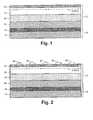
- Figure 1 shows a cross-sectional view of a semiconductor wafer, according to one embodiment of the present invention.
- Figure 1 shows support substrate 10 and III-nitride semiconductor body 12 formed over support substrate 10.
- support substrate 10 comprises first silicon body 14, insulator body 18 over first silicon body 14, and second silicon body 16 over insulator body 18.
- III-nitride semiconductor body 12 comprises III-nitride buffer layer 20, first III-nitride layer 22, and second III-nitride layer 24.
- First silicon body 14 may comprise a ⁇ 100> single crystal silicon
- second silicon body 16 may comprise a ⁇ 111> single crystal silicon, for example.
- both of first silicon body 14 and second silicon body 16 may comprise ⁇ 111> silicon.
- insulator body 18 may be silicon dioxide, for example, and may be implemented so as to electrically isolate first silicon body 14 from second silicon body 16.
- second silicon body 16 may comprise an epitaxially grown silicon layer.
- first silicon body 14 comprises ⁇ 100> silicon and second silicon body 16 comprises ⁇ 111> silicon
- a silicon on insulator (SOI) substrate may be utilized.
- a SOI substrate typically includes two silicon substrate layers bonded to one another by an insulator layer.
- both of first silicon body 14 and second silicon body 16 comprise silicon having the same crystal orientation, such as ⁇ 111>, may be implemented using a Separation-by-Implanted-Oxygen (SIMOX) process.
- SIMOX Separation-by-Implanted-Oxygen
- Insulator body 18 may have a thickness in the range of 0.1 microns to 2.0 microns, for example, such as a thickness of 0.5 microns.
- III-nitride semiconductor body 12 may be characterized by its majority charge carrier conductivity type.
- III-nitride semiconductor body 12 comprises a high electron mobility transistor (HEMT)
- III-nitride semiconductor body 12 may be characterized by the N type conductivity of the majority charge carriers (electrons) populating its two-dimensional electron gas (2DEG).
- HEMT high electron mobility transistor
- III-nitride semiconductor body 12 may comprise an n-channel metal-oxide-semiconductor field-effect transistor (NMOS) device and be characterized by its N type conductivity majority charge carriers (electrons).
- NMOS metal-oxide-semiconductor field-effect transistor
- III-nitride semiconductor body 12 comprises a p-channel metal-oxide-semiconductor field-effect transistor (PMOS) device
- III-nitride semiconductor body 12 may be characterized by the P type conductivity of its majority charge carriers (holes).
- III-nitride semiconductor body 12 may be implemented to comprise such a HEMT.
- III-nitride buffer layer 20 may comprise aluminum nitride (AlN), for example.
- respective first and second III nitride layers 22 and 24 may comprise different III-nitride alloys selected so as to produce a 2DEG near the heterojunction formed at their interface.
- III-nitride semiconductor body 12 may comprise a heterojunction formed at the interface of first III-nitride layer 22 comprising gallium nitride (GaN) and second III-nitride layer 24 comprising aluminum gallium nitride (AlGaN), where first III-nitride layer 22 is formed over second silicon body 16, and second III-nitride layer 24 is formed over first III-nitride layer 22.
- first III-nitride layer 22 and second III-nitride layer 24 may correspond to any suitable combination of one or more group III elements and nitrogen.
- Figure 2 shows a cross-sectional view of a high voltage durability III-nitride semiconductor device, according to one embodiment of the present invention.
- the device shown by Figure 2 may correspond to implementation of III-nitride semiconductor body 12 so as to comprise a HEMT, as described in relation to Figure 1 .
- a device may include first and second power electrodes 26 and 28 (e.g., source and drain electrodes) coupled to the 2DEG through second III-nitride layer 24, and gates 30 situated between respective first and second power electrodes 26 and 28.
- a gate, such as gate 30, may include an insulated gate electrode or a gate electrode that makes a Schottky contact to second III-nitride layer 24, for example.
- the 2DEG represented in Figures 1 and 2 corresponds to a very thin conduction channel populated by highly mobile and highly concentrated electrons that are free to move in the two dimensions of the 2DEG, but, ideally, are constrained from movement in a third dimension perpendicular to the 2DEG, for example, into second silicon body 16.
- application of a few hundred volts to, for example, first power electrode 26, may cause substantial charge leakage through and across second silicon body 16, producing a short between first power electrode 26 and second power electrode 28 through the substrate provided by second silicon body 16, thereby resulting in breakdown of the device.
- a III-nitride semiconductor device may be adapted as a high voltage durability device by ensuring that second silicon body 16 has a conductivity type opposite the majority charge carrier conductivity type of III-nitride semiconductor body 12.
- providing second silicon body 16 having P type conductivity enhances its resistance to breakdown under high applied voltages (e.g., voltages greater than 600 volts).
- a device such as that presently described by reference to Figure 2 can be used for high voltage applications because of the purposeful selection of a conductivity type for second silicon body 16 that is opposite that of the majority charge carrier conductivity type of III-nitride semiconductor body 12.
- such a high voltage durability semiconductor device may exhibit a breakdown voltage exceeding 800 volts, and in some embodiments, breakdown may be avoided up to approximately 1200 volts.
- an SOI substrate may be used in which second silicon body 16 may be doped with P type dopants.
- second silicon body 16 may be P++ doped, and III-nitride semiconductor body 12 capable of producing the 2DEG may be formed over second silicon body 16.
- a P type silicon body may be epitaxially grown over second silicon body 16, and III-nitride semiconductor body 12 may be formed over the P type epitaxial region.
- one side of a first silicon substrate may be implanted with P type dopants, followed by hydrogen implantation close to the final depth of the implanted region. Thereafter, the top surface of the P type region may be oxidized, and a second silicon substrate (e.g., a handle substrate) may be bonded to the oxidized surface.
- the P type region can be cleaved along the hydrogen implant region, and a III-nitride power semiconductor device can be fabricated over the P type region, which constitutes second silicon body 16.
- second silicon body 16 may be implemented to have N type conductivity, such as by being N++ doped, for example.
- various embodiments of the present invention have the further significant advantage of supporting monolithic vertical integration of one or more silicon devices with III-nitride semiconductor body 12.
- electrical isolation of first silicon body 14 and second silicon body 16 from one another, provided by insulator body 18, supports implementation of distinct device types using respective first and second silicon bodies 14 and 16 as independent substrates.
- Use of ⁇ 111> silicon for second silicon body 16 may advantageously support formation of III-nitride semiconductor body 12 using second silicon body 16 as a substrate, for instance.
- Concurrent use of ⁇ 100> silicon for first silicon body 14 may then render first silicon body 14 suitable for use as a substrate for formation of one or more silicon semiconductor devices, such as MOSFETs, on first silicon body 14.
- first and second silicon bodies 14 and 16 can render support substrate 10 capable of concurrently supporting operation of III-nitride power semiconductor devices, and lower power silicon devices.
- first silicon body 14 may be N-doped, N++ doped, P- doped, or P++ doped, for example.
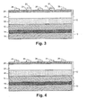
- Figure 3 shows a cross-sectional view of a high voltage durability III-nitride semiconductor device including an insulated gate, according to one embodiment of the present invention.
- Figure 3 shows gates comprising gate dielectric 29 (e.g. silicon dioxide or silicon nitride) situated between gate electrode 31 and second III-nitride layer 24.
- gate dielectric 29 e.g. silicon dioxide or silicon nitride
- Figure 4 shows a cross-sectional view of a high voltage durability III-nitride semiconductor device including a Schottky gate, according to one embodiment of the present invention.
- gate electrode 33 may be configured to make Schottky contact with second III-nitride layer 24.
- a high voltage durability III-nitride power semiconductor device may be an enhancement mode device (e.g., normally OFF when no gate voltage is applied to the gate electrode), or a depletion mode device (e.g., normally ON when no gate voltage is applied to the gate electrode).
- Figure 5 shows a cross-sectional view of an enhancement mode high voltage durability III-nitride semiconductor device including an insulated gate
- Figure 6 shows a cross-sectional view of an enhancement mode high voltage durability III-nitride semiconductor device including a Schottky gate, according to embodiments of the present invention.
- enhancement mode devices may have an interrupted 2DEG directly under the gate which can be restored to allow for current conduction upon application of an appropriate voltage (threshold voltage).
- an appropriate voltage threshold voltage
- Examples of various enhancement mode III-nitride power semiconductor devices can be found in U.S. Patent Application Publication No. 2006/0060871 , which is commonly assigned to the assignee of the present application.
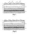
- Figure 7 shows a cross-sectional view of a depletion mode high voltage durability III-nitride semiconductor device including an insulated gate
- Figure 8 shows a cross-sectional view of a depletion mode high voltage durability III-nitride semiconductor device including a Schottky gate, according to embodiments of the present invention.
- depletion mode devices may have an uninterrupted 2DEG directly under the gate which can be interrupted to prevent current conduction upon application of a threshold voltage.
- An Example of a depletion mode III-nitride power semiconductor device is disclosed by U.S. Patent No. 5,192,987 to Khan et al.
- any of the III-nitride semiconductor structures shown by Figure 1 through Figure 8 may be implemented as a high voltage durability semiconductor structure by ensuring that second silicon body 16 has a conductivity type opposite that of type of the majority charge carriers of III-nitride semiconductor body 12.
- support substrate 10 may be utilized to achieve monolithic vertical integration of one or more silicon semiconductor devices with one or more III-nitride power semiconductor devices.
Landscapes
- Junction Field-Effect Transistors (AREA)
- Thin Film Transistor (AREA)
- Insulated Gate Type Field-Effect Transistor (AREA)
Abstract
Description
- The present application is a continuation-in-part of, and claims the benefit of and priority to a pending parent patent application entitled "III-Nitride Wafer and Devices Formed in a III-Nitride Wafer,"
Serial Number 12/324,119, filed on November 26, 2008 - In the present application, "group III-V semiconductor" refers to a compound semiconductor that includes at least one group III element and at least one group V element, such as, but not limited to, gallium nitride (GaN), gallium arsenide (GaAs), indium aluminum gallium nitride (InAlGaN), indium gallium nitride (InGaN) and the like. Analogously, "III-nitride" refers to a compound semiconductor that includes nitrogen and at least one group III element such as, but not limited to, GaN, AlGaN, InN, AlN, InGaN, InAlGaN and the like.
- The present invention is generally in the field of semiconductors. More specifically, the present invention is in the field of fabrication of compound semiconductors.
- Semiconductor based devices, circuits, and switches employed in various modern applications are often required to display greater power handling capabilities and tolerate higher applied voltages than ever before. One response to these increased device performance demands has been the development and implementation of III-nitride semiconductor devices, such as high electron mobility transistors (HEMTs). In a typical HEMT, for example, a two-dimensional electron gas (2DEG) is generated at a semiconductor heterojunction. The 2DEG represents a very thin conduction layer of highly mobile and highly concentrated charge carriers free to move readily in the two dimensions of that conduction layer, but constrained from movement in a third dimension perpendicular to the conduction layer.
- In practice, the ability of a HEMT, or any III-nitride semiconductor device, to perform reliably in the face of a high applied voltage (e.g. voltage greater than 600 volts), depends in part on the charge retention characteristics of the 2DEG or other type of conduction channel. In particular, where charge carriers are insufficiently constrained from dispersing out of a desired conduction zone, for example by movement into a silicon substrate of the device, device performance may be less than optimal. More seriously, under applied voltages of even a few hundred volts, a HEMT may short through its silicon substrate, resulting in device failure. Unfortunately, conventional approaches to III-nitride semiconductor device fabrication have failed to provide optimal charge carrier constraint within the conduction zone when high voltage is applied.
- Thus, there is a need to overcome the drawbacks and deficiencies in the art by providing a III-nitride semiconductor device, such as a HEMT, exhibiting high voltage durability. It would be of additional advantage if the proposed solution were to provide an implementation capable of supporting monolithic vertical integration of III-nitride power semiconductor devices and silicon devices.
- A high voltage durability III-nitride semiconductor device, substantially as shown in and/or described in connection with at least one of the figures, as set forth more completely in the claims.
-
-
Figure 1 shows a cross-sectional view of a semiconductor wafer, according to one embodiment of the present invention. -
Figure 2 shows a cross-sectional view of a high voltage durability III-nitride semiconductor device, according to one embodiment of the present invention. -
Figure 3 shows a cross-sectional view of a high voltage durability III-nitride semiconductor device including an insulated gate, according to one embodiment of the present invention. -
Figure 4 shows a cross-sectional view of a high voltage durability III-nitride semiconductor device including a Schottky gate, according to one embodiment of the present invention. -
Figure 5 shows a cross-sectional view of an enhancement mode high voltage durability III-nitride semiconductor device including an insulated gate, according to one embodiment of the present invention. -
Figure 6 shows a cross-sectional view of an enhancement mode high voltage durability III-nitride semiconductor device including a Schottky gate, according to one embodiment of the present invention. -
Figure 7 shows a cross-sectional view of a depletion mode high voltage durability III-nitride semiconductor device including an insulated gate, according to one embodiment of the present invention. -
Figure 8 shows a cross-sectional view of a depletion mode high voltage durability III-nitride semiconductor device including a Schottky gate, according to one embodiment of the present invention. - The present invention is directed to a high durability III-nitride semiconductor device. Although the invention is described with respect to specific embodiments, the principles of the invention, as defined by the claims appended herein, can obviously be applied beyond the specifically described embodiments of the invention described herein. Moreover, in the description of the present invention, certain details have been left out in order to not obscure the inventive aspects of the invention. The details left out are within the knowledge of a person of ordinary skill in the art.
- The drawings in the present application and their accompanying detailed description are directed to merely example embodiments of the invention. To maintain brevity, other embodiments of the invention, which use the principles of the present invention, are not specifically described in the present application and are not specifically illustrated by the present drawings. It should be borne in mind that, unless noted otherwise, like or corresponding elements among the figures may be indicated by like or corresponding reference numerals.
-
Figure 1 shows a cross-sectional view of a semiconductor wafer, according to one embodiment of the present invention.Figure 1 showssupport substrate 10 and III-nitride semiconductor body 12 formed oversupport substrate 10. According to the embodiment ofFigure 1 ,support substrate 10 comprisesfirst silicon body 14,insulator body 18 overfirst silicon body 14, andsecond silicon body 16 overinsulator body 18. As further shown byFigure 1 , III-nitride semiconductor body 12 comprises III-nitride buffer layer 20, first III-nitride layer 22, and second III-nitride layer 24. -
First silicon body 14 may comprise a <100> single crystal silicon, andsecond silicon body 16 may comprise a <111> single crystal silicon, for example. Alternatively, both offirst silicon body 14 andsecond silicon body 16 may comprise <111> silicon. In either instance,insulator body 18 may be silicon dioxide, for example, and may be implemented so as to electrically isolatefirst silicon body 14 fromsecond silicon body 16. It is noted that in some embodiments,second silicon body 16 may comprise an epitaxially grown silicon layer. - In embodiments in which
first silicon body 14 comprises <100> silicon andsecond silicon body 16 comprises <111> silicon, as well in those in which both offirst silicon body 14 andsecond silicon body 16 have the same silicon crystal orientation, a silicon on insulator (SOI) substrate may be utilized. A SOI substrate typically includes two silicon substrate layers bonded to one another by an insulator layer. Alternatively, embodiments in which both offirst silicon body 14 andsecond silicon body 16 comprise silicon having the same crystal orientation, such as <111>, may be implemented using a Separation-by-Implanted-Oxygen (SIMOX) process. For example, implantation of oxygen into a <111> silicon substrate followed by an annealing step would result ininsulator body 18 being formed betweenfirst silicon body 14 andsecond silicon body 16, as shown inFigure 1 .Insulator body 18 may have a thickness in the range of 0.1 microns to 2.0 microns, for example, such as a thickness of 0.5 microns. - III-
nitride semiconductor body 12 may be characterized by its majority charge carrier conductivity type. For example, as represented inFigure 1 , where III-nitride semiconductor body 12 comprises a high electron mobility transistor (HEMT), III-nitride semiconductor body 12 may be characterized by the N type conductivity of the majority charge carriers (electrons) populating its two-dimensional electron gas (2DEG). Similarly, in another embodiment, III-nitride semiconductor body 12 may comprise an n-channel metal-oxide-semiconductor field-effect transistor (NMOS) device and be characterized by its N type conductivity majority charge carriers (electrons). Analogously, where III-nitride semiconductor body 12 comprises a p-channel metal-oxide-semiconductor field-effect transistor (PMOS) device, III-nitride semiconductor body 12 may be characterized by the P type conductivity of its majority charge carriers (holes). - As shown by
Figure 1 , for example, in one embodiment, III-nitride semiconductor body 12 may be implemented to comprise such a HEMT. According to that embodiment, III-nitride buffer layer 20 may comprise aluminum nitride (AlN), for example. In addition, respective first and secondIII nitride layers nitride semiconductor body 12 may comprise a heterojunction formed at the interface of first III-nitride layer 22 comprising gallium nitride (GaN) and second III-nitride layer 24 comprising aluminum gallium nitride (AlGaN), where first III-nitride layer 22 is formed oversecond silicon body 16, and second III-nitride layer 24 is formed over first III-nitride layer 22. More generally, as set forth in the definition section above, first III-nitride layer 22 and second III-nitride layer 24 may correspond to any suitable combination of one or more group III elements and nitrogen. - Turning to
Figure 2, Figure 2 shows a cross-sectional view of a high voltage durability III-nitride semiconductor device, according to one embodiment of the present invention. The device shown byFigure 2 may correspond to implementation of III-nitride semiconductor body 12 so as to comprise a HEMT, as described in relation toFigure 1 . As shown inFigure 2 , such a device may include first andsecond power electrodes 26 and 28 (e.g., source and drain electrodes) coupled to the 2DEG through second III-nitride layer 24, andgates 30 situated between respective first andsecond power electrodes gate 30, may include an insulated gate electrode or a gate electrode that makes a Schottky contact to second III-nitride layer 24, for example. - The 2DEG represented in
Figures 1 and 2 corresponds to a very thin conduction channel populated by highly mobile and highly concentrated electrons that are free to move in the two dimensions of the 2DEG, but, ideally, are constrained from movement in a third dimension perpendicular to the 2DEG, for example, intosecond silicon body 16. In practice, however, application of a few hundred volts to, for example,first power electrode 26, may cause substantial charge leakage through and acrosssecond silicon body 16, producing a short betweenfirst power electrode 26 andsecond power electrode 28 through the substrate provided bysecond silicon body 16, thereby resulting in breakdown of the device. - As described herein, a III-nitride semiconductor device may be adapted as a high voltage durability device by ensuring that
second silicon body 16 has a conductivity type opposite the majority charge carrier conductivity type of III-nitride semiconductor body 12. Thus, in the presence of the 2DEG shown inFigure 2 , providingsecond silicon body 16 having P type conductivity enhances its resistance to breakdown under high applied voltages (e.g., voltages greater than 600 volts). A device such as that presently described by reference toFigure 2 can be used for high voltage applications because of the purposeful selection of a conductivity type forsecond silicon body 16 that is opposite that of the majority charge carrier conductivity type of III-nitride semiconductor body 12. In some embodiments, for instance, such a high voltage durability semiconductor device may exhibit a breakdown voltage exceeding 800 volts, and in some embodiments, breakdown may be avoided up to approximately 1200 volts. - In one embodiment, an SOI substrate may be used in which
second silicon body 16 may be doped with P type dopants. For example,second silicon body 16 may be P++ doped, and III-nitride semiconductor body 12 capable of producing the 2DEG may be formed oversecond silicon body 16. Alternatively, a P type silicon body may be epitaxially grown oversecond silicon body 16, and III-nitride semiconductor body 12 may be formed over the P type epitaxial region. - In another embodiment, one side of a first silicon substrate may be implanted with P type dopants, followed by hydrogen implantation close to the final depth of the implanted region. Thereafter, the top surface of the P type region may be oxidized, and a second silicon substrate (e.g., a handle substrate) may be bonded to the oxidized surface. The P type region can be cleaved along the hydrogen implant region, and a III-nitride power semiconductor device can be fabricated over the P type region, which constitutes
second silicon body 16. It is noted than when appropriate, such as when III-nitride semiconductor body 12 comprises a device having P type majority charge carriers,second silicon body 16 may be implemented to have N type conductivity, such as by being N++ doped, for example. - In addition to high voltage durability flowing from appropriate conductivity type selection for
second silicon body 16, various embodiments of the present invention have the further significant advantage of supporting monolithic vertical integration of one or more silicon devices with III-nitride semiconductor body 12. For example, electrical isolation offirst silicon body 14 andsecond silicon body 16 from one another, provided byinsulator body 18, supports implementation of distinct device types using respective first andsecond silicon bodies second silicon body 16 may advantageously support formation of III-nitride semiconductor body 12 usingsecond silicon body 16 as a substrate, for instance. Concurrent use of <100> silicon forfirst silicon body 14 may then renderfirst silicon body 14 suitable for use as a substrate for formation of one or more silicon semiconductor devices, such as MOSFETs, onfirst silicon body 14. - Thus, appropriate selection of silicon crystal orientations for respective first and
second silicon bodies support substrate 10 capable of concurrently supporting operation of III-nitride power semiconductor devices, and lower power silicon devices. Depending upon the desired implementation,first silicon body 14 may be N-doped, N++ doped, P- doped, or P++ doped, for example. - Referring now to
Figure 3, Figure 3 shows a cross-sectional view of a high voltage durability III-nitride semiconductor device including an insulated gate, according to one embodiment of the present invention.Figure 3 shows gates comprising gate dielectric 29 (e.g. silicon dioxide or silicon nitride) situated betweengate electrode 31 and second III-nitride layer 24. -
Figure 4 shows a cross-sectional view of a high voltage durability III-nitride semiconductor device including a Schottky gate, according to one embodiment of the present invention. As shown inFigure 4 , in this latter embodiment,gate electrode 33 may be configured to make Schottky contact with second III-nitride layer 24. - Moreover, a high voltage durability III-nitride power semiconductor device may be an enhancement mode device (e.g., normally OFF when no gate voltage is applied to the gate electrode), or a depletion mode device (e.g., normally ON when no gate voltage is applied to the gate electrode).
Figure 5 shows a cross-sectional view of an enhancement mode high voltage durability III-nitride semiconductor device including an insulated gate, whileFigure 6 shows a cross-sectional view of an enhancement mode high voltage durability III-nitride semiconductor device including a Schottky gate, according to embodiments of the present invention. As shown inFigures 5 and 6 , such enhancement mode devices may have an interrupted 2DEG directly under the gate which can be restored to allow for current conduction upon application of an appropriate voltage (threshold voltage). Examples of various enhancement mode III-nitride power semiconductor devices can be found inU.S. Patent Application Publication No. 2006/0060871 , which is commonly assigned to the assignee of the present application. -
Figure 7 shows a cross-sectional view of a depletion mode high voltage durability III-nitride semiconductor device including an insulated gate, whileFigure 8 shows a cross-sectional view of a depletion mode high voltage durability III-nitride semiconductor device including a Schottky gate, according to embodiments of the present invention. As shown inFigures 7 and 8 , such depletion mode devices may have an uninterrupted 2DEG directly under the gate which can be interrupted to prevent current conduction upon application of a threshold voltage. An Example of a depletion mode III-nitride power semiconductor device is disclosed byU.S. Patent No. 5,192,987 to Khan et al. - Thus, any of the III-nitride semiconductor structures shown by
Figure 1 through Figure 8 may be implemented as a high voltage durability semiconductor structure by ensuring thatsecond silicon body 16 has a conductivity type opposite that of type of the majority charge carriers of III-nitride semiconductor body 12. In addition, by utilizing <100> silicon forfirst silicon body 14,support substrate 10 may be utilized to achieve monolithic vertical integration of one or more silicon semiconductor devices with one or more III-nitride power semiconductor devices. - From the above description of the invention it is manifest that various techniques can be used for implementing the concepts of the present invention without departing from its scope. Moreover, while the invention has been described with specific reference to certain embodiments, a person of ordinary skill in the art would recognize that changes can be made in form and detail without departing from the spirit and the scope of the invention. The described embodiments are to be considered in all respects as illustrative and not restrictive. It should also be understood that the invention is not limited to the particular embodiments described herein, but is capable of many rearrangements, modifications, and substitutions without departing from the scope of the invention.
Claims (20)
- A high voltage durability III-nitride semiconductor device comprising:a support substrate including a first silicon body, an insulator body over said first silicon body, and a second silicon body over said insulator body;a III-nitride semiconductor body formed over said second silicon body, said III-nitride semiconductor body characterized by a majority charge carrier conductivity type;said second silicon body having a conductivity type opposite said majority charge carrier conductivity type.
- The high voltage durability III-nitride semiconductor device of claim 1, wherein a breakdown voltage of said high voltage durability III-nitride semiconductor device is greater than 800 volts.
- The high voltage durability III-nitride semiconductor device of claim 1, wherein said III-nitride semiconductor body comprises a heterojunction formed at an interface of a first III-nitride layer and a second III-nitride layer.
- The high voltage durability III-nitride semiconductor device of claim 3, wherein said first III-nitride layer comprises gallium nitride (GaN) and said second III-nitride layer comprises aluminum gallium nitride (AlGaN).
- The high voltage durability III-nitride semiconductor device of claim 1, wherein said III-nitride semiconductor body comprises a high electron mobility transistor (HEMT).
- The high voltage durability III-nitride semiconductor device of claim 1, wherein said second silicon body has P type conductivity.
- The high voltage durability III-nitride semiconductor device of claim 1, wherein said second silicon body comprises <111> silicon.
- The high voltage durability III-nitride semiconductor device of claim 1, wherein said first silicon body comprises <100> silicon.
- The high voltage durability III-nitride semiconductor device of claim 1, wherein said first silicon body is N- doped.
- The high voltage durability III-nitride semiconductor device of claim 1, wherein said first silicon body is P- doped.
- The high voltage durability III-nitride semiconductor device of claim 1, further comprising a silicon semiconductor device formed on said first silicon body.
- The high voltage durability III-nitride semiconductor device of claim 11, wherein said silicon semiconductor device comprises a metal-oxide-semiconductor field-effect transistor (MOSFET).
- The high voltage durability III-nitride semiconductor device of claim 1, wherein said III-nitride body comprises a PMOS device.
- The high voltage durability III-nitride semiconductor device of claim 13, wherein said second silicon body has N type conductivity.
- The high voltage durability III-nitride semiconductor device of claim 1, further comprising power electrodes formed over said III-nitride body.
- The high voltage durability III-nitride semiconductor device of claim 15, further comprising a gate situated between said power electrodes.
- The high voltage durability III-nitride semiconductor device of claim 16, wherein said gate comprises a gate dielectric and a gate electrode.
- The high voltage durability III-nitride semiconductor device of claim 16, wherein said III-nitride body includes a III-nitride heterojunction having a two-dimensional electron gas that includes an interrupted region under said gate.
- A high voltage durability, high electron mobility transistor (HEMT), said high voltage durability HEMT comprising:a support substrate including a <100> silicon layer, an insulator layer over said <100> silicon layer, and a P type conductivity <111> silicon layer over said insulator layer;a III-nitride semiconductor body formed over said P type conductivity <111> silicon layer, said III-nitride semiconductor body forming a heterojunction of said HEMT.
- The high voltage durability HEMT of claim 19, wherein a breakdown voltage of said HEMT is greater than 800 volts.
Applications Claiming Priority (1)
| Application Number | Priority Date | Filing Date | Title |
|---|---|---|---|
| US12/653,467 US7999288B2 (en) | 2007-11-26 | 2009-12-14 | High voltage durability III-nitride semiconductor device |
Publications (3)
| Publication Number | Publication Date |
|---|---|
| EP2333822A2 true EP2333822A2 (en) | 2011-06-15 |
| EP2333822A3 EP2333822A3 (en) | 2011-10-12 |
| EP2333822B1 EP2333822B1 (en) | 2019-01-30 |
Family
ID=43735846
Family Applications (1)
| Application Number | Title | Priority Date | Filing Date |
|---|---|---|---|
| EP10015287.5A Active EP2333822B1 (en) | 2009-12-14 | 2010-12-03 | High voltage durability III-nitride semiconductor device |
Country Status (3)
| Country | Link |
|---|---|
| US (3) | US7999288B2 (en) |
| EP (1) | EP2333822B1 (en) |
| JP (1) | JP2011124572A (en) |
Families Citing this family (30)
| Publication number | Priority date | Publication date | Assignee | Title |
|---|---|---|---|---|
| US7999288B2 (en) * | 2007-11-26 | 2011-08-16 | International Rectifier Corporation | High voltage durability III-nitride semiconductor device |
| US8159003B2 (en) * | 2007-11-26 | 2012-04-17 | International Rectifier Corporation | III-nitride wafer and devices formed in a III-nitride wafer |
| US8981380B2 (en) * | 2010-03-01 | 2015-03-17 | International Rectifier Corporation | Monolithic integration of silicon and group III-V devices |
| US9219058B2 (en) * | 2010-03-01 | 2015-12-22 | Infineon Technologies Americas Corp. | Efficient high voltage switching circuits and monolithic integration of same |
| US9647076B2 (en) | 2011-11-21 | 2017-05-09 | Sensor Electronic Technology, Inc. | Circuit including semiconductor device with multiple individually biased space-charge control electrodes |
| US9673285B2 (en) | 2011-11-21 | 2017-06-06 | Sensor Electronic Technology, Inc. | Semiconductor device with low-conducting buried and/or surface layers |
| KR101913387B1 (en) | 2012-03-23 | 2018-10-30 | 삼성전자주식회사 | Selective low-temperature ohmic contact formation method for ⅲ-nitride heterostructure device |
| JP6054620B2 (en) * | 2012-03-29 | 2016-12-27 | トランスフォーム・ジャパン株式会社 | Compound semiconductor device and manufacturing method thereof |
| US20140197461A1 (en) | 2013-01-14 | 2014-07-17 | International Rectifier Corporation | Semiconductor Structure Including A Spatially Confined Dielectric Region |
| US9978862B2 (en) | 2013-04-30 | 2018-05-22 | Infineon Technologies Austria Ag | Power transistor with at least partially integrated driver stage |
| US9799643B2 (en) * | 2013-05-23 | 2017-10-24 | Infineon Technologies Austria Ag | Gate voltage control for III-nitride transistors |
| US10312360B2 (en) | 2013-06-18 | 2019-06-04 | Stephen P. Barlow | Method for producing trench high electron mobility devices |
| US20150079738A1 (en) * | 2013-06-18 | 2015-03-19 | Stephen P. Barlow | Method for producing trench high electron mobility devices |
| US9245991B2 (en) | 2013-08-12 | 2016-01-26 | Taiwan Semiconductor Manufacturing Company, Ltd. | Semiconductor device, high electron mobility transistor (HEMT) and method of manufacturing |
| JP6133191B2 (en) * | 2013-10-18 | 2017-05-24 | 古河電気工業株式会社 | Nitride semiconductor device, diode, and field effect transistor |
| US20150162832A1 (en) | 2013-12-09 | 2015-06-11 | International Rectifier Corporation | Group III-V Voltage Converter with Monolithically Integrated Level Shifter, High Side Driver, and High Side Power Switch |
| WO2016100805A1 (en) * | 2014-12-19 | 2016-06-23 | Sensor Electronic Technology, Inc. | Semiconductor device with multiple space-charge control electrodes |
| WO2016154965A1 (en) | 2015-04-01 | 2016-10-06 | Xin Yingwei | Structured item organizing mechanism in e-commerce |
| US10002956B1 (en) * | 2017-08-31 | 2018-06-19 | Vanguard International Semiconductor Corporation | High electron mobility transistor |
| US10564356B2 (en) * | 2017-11-16 | 2020-02-18 | Samsung Electronics Co., Ltd. | Heterogeneous integrated circuit for short wavelengths |
| US11393765B2 (en) | 2017-11-16 | 2022-07-19 | Samsung Electronics Co., Ltd. | Heterogeneous integrated circuit for short wavelengths |
| US10644142B2 (en) | 2017-12-22 | 2020-05-05 | Nxp Usa, Inc. | Semiconductor devices with doped regions functioning as enhanced resistivity regions or diffusion barriers, and methods of fabrication therefor |
| US10103239B1 (en) * | 2017-12-28 | 2018-10-16 | Vanguard International Semiconductor Corporation | High electron mobility transistor structure |
| JP6863423B2 (en) * | 2019-08-06 | 2021-04-21 | 信越半導体株式会社 | Substrates for electronic devices and their manufacturing methods |
| JP6679036B1 (en) * | 2019-11-29 | 2020-04-15 | 株式会社パウデック | Diode, method of manufacturing diode, and electric device |
| CN113508467A (en) * | 2021-03-30 | 2021-10-15 | 英诺赛科(苏州)科技有限公司 | Group III nitride semiconductor devices on patterned substrates |
| US12218202B2 (en) * | 2021-09-16 | 2025-02-04 | Wolfspeed, Inc. | Semiconductor device incorporating a substrate recess |
| US12324179B2 (en) * | 2021-12-16 | 2025-06-03 | Wolfspeed, Inc. | Group III-nitride high-electron mobility transistors with a buried metallic conductive material layer and process for making the same |
| FR3131075B1 (en) * | 2021-12-16 | 2023-12-22 | Soitec Silicon On Insulator | GROUP III NITRIDE SEMICONDUCTOR STRUCTURE ON SILICON ON INSULATION AND ITS GROWTH METHOD |
| FR3161798B1 (en) * | 2024-04-29 | 2026-04-24 | Soitec Belgium | SEMICONDUCTIVE STRUCTURE AND MANUFACTURING METHOD FOR MONOLITHIC INTEGRATION OF FUNCTIONALITIES |
Citations (2)
| Publication number | Priority date | Publication date | Assignee | Title |
|---|---|---|---|---|
| US5192987A (en) | 1991-05-17 | 1993-03-09 | Apa Optics, Inc. | High electron mobility transistor with GaN/Alx Ga1-x N heterojunctions |
| US20060060871A1 (en) | 2004-01-23 | 2006-03-23 | International Rectifier Corp. | Enhancement mode III-nitride FET |
Family Cites Families (23)
| Publication number | Priority date | Publication date | Assignee | Title |
|---|---|---|---|---|
| US4774205A (en) | 1986-06-13 | 1988-09-27 | Massachusetts Institute Of Technology | Monolithic integration of silicon and gallium arsenide devices |
| US4940672A (en) | 1989-03-17 | 1990-07-10 | Kopin Corporation | Method of making monolithic integrated III-V type laser devices and silicon devices on silicon |
| US20040129200A1 (en) * | 2001-09-26 | 2004-07-08 | John Kouvetakis | Active electronic devices based on gallium nitride and its alloys grown on silicon substrates with buffer layers of SiCAIN |
| JP2003347523A (en) * | 2002-05-27 | 2003-12-05 | Denso Corp | Semiconductor device |
| JP4192009B2 (en) | 2003-02-24 | 2008-12-03 | 寛治 大塚 | Electronic circuit equipment |
| EP1634323A4 (en) * | 2003-06-13 | 2008-06-04 | Univ North Carolina State | COMPLEX OXIDES FOR USE IN SEMICONDUCTOR DEVICES AND ASSOCIATED METHODS |
| JP2007246289A (en) * | 2004-03-11 | 2007-09-27 | Nec Corp | Method for manufacturing gallium nitride based semiconductor substrate |
| US7361946B2 (en) * | 2004-06-28 | 2008-04-22 | Nitronex Corporation | Semiconductor device-based sensors |
| US7247889B2 (en) * | 2004-12-03 | 2007-07-24 | Nitronex Corporation | III-nitride material structures including silicon substrates |
| JP4645313B2 (en) * | 2005-06-14 | 2011-03-09 | 富士電機システムズ株式会社 | Semiconductor device |
| US8866190B2 (en) | 2005-06-14 | 2014-10-21 | International Rectifler Corporation | Methods of combining silicon and III-nitride material on a single wafer |
| DE112006001751B4 (en) | 2005-07-06 | 2010-04-08 | International Rectifier Corporation, El Segundo | Power semiconductor device and method for manufacturing a semiconductor device |
| CN101326646B (en) | 2005-11-01 | 2011-03-16 | 麻省理工学院 | Monolithically integrated semiconductor materials and devices |
| JP2008034411A (en) * | 2006-07-26 | 2008-02-14 | Toshiba Corp | Nitride semiconductor device |
| JP2008141187A (en) * | 2006-11-09 | 2008-06-19 | Matsushita Electric Ind Co Ltd | Nitride semiconductor laser device |
| FR2908925B1 (en) | 2006-11-17 | 2009-02-20 | St Microelectronics Sa | METHOD FOR INTEGRATING A III-N TYPE COMPONENT, SUCH AS GAS, ON A NOMINAL SILICON (001) SUBSTRATE |
| JP2008153330A (en) | 2006-12-15 | 2008-07-03 | Oki Electric Ind Co Ltd | Nitride semiconductor high electron mobility transistor |
| US20090050939A1 (en) * | 2007-07-17 | 2009-02-26 | Briere Michael A | Iii-nitride device |
| US7999288B2 (en) * | 2007-11-26 | 2011-08-16 | International Rectifier Corporation | High voltage durability III-nitride semiconductor device |
| US8159003B2 (en) * | 2007-11-26 | 2012-04-17 | International Rectifier Corporation | III-nitride wafer and devices formed in a III-nitride wafer |
| JP5470705B2 (en) * | 2007-12-28 | 2014-04-16 | サンケン電気株式会社 | Semiconductor device and manufacturing method thereof |
| US20090261346A1 (en) * | 2008-04-16 | 2009-10-22 | Ding-Yuan Chen | Integrating CMOS and Optical Devices on a Same Chip |
| US8703623B2 (en) * | 2009-06-01 | 2014-04-22 | Massachusetts Institute Of Technology | Fabrication technique for gallium nitride substrates |
-
2009
- 2009-12-14 US US12/653,467 patent/US7999288B2/en not_active Expired - Fee Related
-
2010
- 2010-12-03 EP EP10015287.5A patent/EP2333822B1/en active Active
- 2010-12-06 JP JP2010271293A patent/JP2011124572A/en active Pending
-
2011
- 2011-08-03 US US13/197,676 patent/US20110284869A1/en not_active Abandoned
-
2014
- 2014-08-14 US US14/459,726 patent/US9281387B2/en active Active
Patent Citations (2)
| Publication number | Priority date | Publication date | Assignee | Title |
|---|---|---|---|---|
| US5192987A (en) | 1991-05-17 | 1993-03-09 | Apa Optics, Inc. | High electron mobility transistor with GaN/Alx Ga1-x N heterojunctions |
| US20060060871A1 (en) | 2004-01-23 | 2006-03-23 | International Rectifier Corp. | Enhancement mode III-nitride FET |
Also Published As
| Publication number | Publication date |
|---|---|
| US7999288B2 (en) | 2011-08-16 |
| US20110284869A1 (en) | 2011-11-24 |
| US20100096668A1 (en) | 2010-04-22 |
| EP2333822A3 (en) | 2011-10-12 |
| US20140353723A1 (en) | 2014-12-04 |
| EP2333822B1 (en) | 2019-01-30 |
| US9281387B2 (en) | 2016-03-08 |
| JP2011124572A (en) | 2011-06-23 |
Similar Documents
| Publication | Publication Date | Title |
|---|---|---|
| EP2333822B1 (en) | High voltage durability III-nitride semiconductor device | |
| US8809909B2 (en) | High voltage III-nitride transistor | |
| US10411008B2 (en) | System and method for depletion mode and enhancement mode transistors | |
| US9570438B1 (en) | Avalanche-rugged quasi-vertical HEMT | |
| US9105499B1 (en) | Complementary field effect transistors using gallium polar and nitrogen polar III-nitride material | |
| US9343562B2 (en) | Dual-gated group III-V merged transistor | |
| US9793259B2 (en) | Integrated semiconductor device | |
| US8552471B2 (en) | Semiconductor apparatus having reverse blocking characteristics and method of manufacturing the same | |
| US8895993B2 (en) | Low gate-leakage structure and method for gallium nitride enhancement mode transistor | |
| US8969881B2 (en) | Power transistor having segmented gate | |
| US20120305987A1 (en) | Lateral trench mesfet | |
| US9059239B2 (en) | Bidirectional transistor with optimized high electron mobility current | |
| US10636899B2 (en) | High electron mobility transistor with graded back-barrier region | |
| WO2010042479A2 (en) | Enhancement-mode nitride transistor | |
| JP5526174B2 (en) | Composite semiconductor device with turn-on prevention | |
| KR100857683B1 (en) | Nitride semiconductor device and its manufacturing method | |
| US8698232B2 (en) | Semiconductor device including a voltage controlled termination structure and method for fabricating same | |
| US8637924B2 (en) | Lateral trench MESFET |
Legal Events
| Date | Code | Title | Description |
|---|---|---|---|
| PUAI | Public reference made under article 153(3) epc to a published international application that has entered the european phase |
Free format text: ORIGINAL CODE: 0009012 |
|
| AK | Designated contracting states |
Kind code of ref document: A2 Designated state(s): AL AT BE BG CH CY CZ DE DK EE ES FI FR GB GR HR HU IE IS IT LI LT LU LV MC MK MT NL NO PL PT RO RS SE SI SK SM TR |
|
| AX | Request for extension of the european patent |
Extension state: BA ME |
|
| PUAL | Search report despatched |
Free format text: ORIGINAL CODE: 0009013 |
|
| AK | Designated contracting states |
Kind code of ref document: A3 Designated state(s): AL AT BE BG CH CY CZ DE DK EE ES FI FR GB GR HR HU IE IS IT LI LT LU LV MC MK MT NL NO PL PT RO RS SE SI SK SM TR |
|
| AX | Request for extension of the european patent |
Extension state: BA ME |
|
| RIC1 | Information provided on ipc code assigned before grant |
Ipc: H01L 21/335 20060101AFI20110907BHEP Ipc: H01L 29/20 20060101ALI20110907BHEP Ipc: H01L 29/04 20060101ALI20110907BHEP Ipc: H01L 29/778 20060101ALI20110907BHEP |
|
| 17P | Request for examination filed |
Effective date: 20111028 |
|
| 17Q | First examination report despatched |
Effective date: 20130710 |
|
| STAA | Information on the status of an ep patent application or granted ep patent |
Free format text: STATUS: EXAMINATION IS IN PROGRESS |
|
| REG | Reference to a national code |
Ref country code: DE Ref legal event code: R079 Ref document number: 602010056834 Country of ref document: DE Free format text: PREVIOUS MAIN CLASS: H01L0021335000 Ipc: H01L0027060000 |
|
| GRAP | Despatch of communication of intention to grant a patent |
Free format text: ORIGINAL CODE: EPIDOSNIGR1 |
|
| STAA | Information on the status of an ep patent application or granted ep patent |
Free format text: STATUS: GRANT OF PATENT IS INTENDED |
|
| RIC1 | Information provided on ipc code assigned before grant |
Ipc: H01L 27/06 20060101AFI20180627BHEP Ipc: H01L 29/778 20060101ALI20180627BHEP |
|
| INTG | Intention to grant announced |
Effective date: 20180801 |
|
| RAP1 | Party data changed (applicant data changed or rights of an application transferred) |
Owner name: INFINEON TECHNOLOGIES AMERICAS CORP. |
|
| GRAS | Grant fee paid |
Free format text: ORIGINAL CODE: EPIDOSNIGR3 |
|
| GRAA | (expected) grant |
Free format text: ORIGINAL CODE: 0009210 |
|
| STAA | Information on the status of an ep patent application or granted ep patent |
Free format text: STATUS: THE PATENT HAS BEEN GRANTED |
|
| AK | Designated contracting states |
Kind code of ref document: B1 Designated state(s): AL AT BE BG CH CY CZ DE DK EE ES FI FR GB GR HR HU IE IS IT LI LT LU LV MC MK MT NL NO PL PT RO RS SE SI SK SM TR |
|
| REG | Reference to a national code |
Ref country code: GB Ref legal event code: FG4D |
|
| REG | Reference to a national code |
Ref country code: CH Ref legal event code: EP |
|
| REG | Reference to a national code |
Ref country code: AT Ref legal event code: REF Ref document number: 1093938 Country of ref document: AT Kind code of ref document: T Effective date: 20190215 |
|
| REG | Reference to a national code |
Ref country code: IE Ref legal event code: FG4D |
|
| REG | Reference to a national code |
Ref country code: DE Ref legal event code: R096 Ref document number: 602010056834 Country of ref document: DE |
|
| REG | Reference to a national code |
Ref country code: DE Ref legal event code: R082 Ref document number: 602010056834 Country of ref document: DE |
|
| REG | Reference to a national code |
Ref country code: LT Ref legal event code: MG4D |
|
| REG | Reference to a national code |
Ref country code: NL Ref legal event code: MP Effective date: 20190130 |
|
| PG25 | Lapsed in a contracting state [announced via postgrant information from national office to epo] |
Ref country code: NL Free format text: LAPSE BECAUSE OF FAILURE TO SUBMIT A TRANSLATION OF THE DESCRIPTION OR TO PAY THE FEE WITHIN THE PRESCRIBED TIME-LIMIT Effective date: 20190130 Ref country code: SE Free format text: LAPSE BECAUSE OF FAILURE TO SUBMIT A TRANSLATION OF THE DESCRIPTION OR TO PAY THE FEE WITHIN THE PRESCRIBED TIME-LIMIT Effective date: 20190130 Ref country code: PL Free format text: LAPSE BECAUSE OF FAILURE TO SUBMIT A TRANSLATION OF THE DESCRIPTION OR TO PAY THE FEE WITHIN THE PRESCRIBED TIME-LIMIT Effective date: 20190130 Ref country code: LT Free format text: LAPSE BECAUSE OF FAILURE TO SUBMIT A TRANSLATION OF THE DESCRIPTION OR TO PAY THE FEE WITHIN THE PRESCRIBED TIME-LIMIT Effective date: 20190130 Ref country code: ES Free format text: LAPSE BECAUSE OF FAILURE TO SUBMIT A TRANSLATION OF THE DESCRIPTION OR TO PAY THE FEE WITHIN THE PRESCRIBED TIME-LIMIT Effective date: 20190130 Ref country code: FI Free format text: LAPSE BECAUSE OF FAILURE TO SUBMIT A TRANSLATION OF THE DESCRIPTION OR TO PAY THE FEE WITHIN THE PRESCRIBED TIME-LIMIT Effective date: 20190130 Ref country code: PT Free format text: LAPSE BECAUSE OF FAILURE TO SUBMIT A TRANSLATION OF THE DESCRIPTION OR TO PAY THE FEE WITHIN THE PRESCRIBED TIME-LIMIT Effective date: 20190530 Ref country code: NO Free format text: LAPSE BECAUSE OF FAILURE TO SUBMIT A TRANSLATION OF THE DESCRIPTION OR TO PAY THE FEE WITHIN THE PRESCRIBED TIME-LIMIT Effective date: 20190430 |
|
| REG | Reference to a national code |
Ref country code: AT Ref legal event code: MK05 Ref document number: 1093938 Country of ref document: AT Kind code of ref document: T Effective date: 20190130 |
|
| PG25 | Lapsed in a contracting state [announced via postgrant information from national office to epo] |
Ref country code: BG Free format text: LAPSE BECAUSE OF FAILURE TO SUBMIT A TRANSLATION OF THE DESCRIPTION OR TO PAY THE FEE WITHIN THE PRESCRIBED TIME-LIMIT Effective date: 20190430 Ref country code: GR Free format text: LAPSE BECAUSE OF FAILURE TO SUBMIT A TRANSLATION OF THE DESCRIPTION OR TO PAY THE FEE WITHIN THE PRESCRIBED TIME-LIMIT Effective date: 20190501 Ref country code: IS Free format text: LAPSE BECAUSE OF FAILURE TO SUBMIT A TRANSLATION OF THE DESCRIPTION OR TO PAY THE FEE WITHIN THE PRESCRIBED TIME-LIMIT Effective date: 20190530 Ref country code: LV Free format text: LAPSE BECAUSE OF FAILURE TO SUBMIT A TRANSLATION OF THE DESCRIPTION OR TO PAY THE FEE WITHIN THE PRESCRIBED TIME-LIMIT Effective date: 20190130 Ref country code: HR Free format text: LAPSE BECAUSE OF FAILURE TO SUBMIT A TRANSLATION OF THE DESCRIPTION OR TO PAY THE FEE WITHIN THE PRESCRIBED TIME-LIMIT Effective date: 20190130 Ref country code: RS Free format text: LAPSE BECAUSE OF FAILURE TO SUBMIT A TRANSLATION OF THE DESCRIPTION OR TO PAY THE FEE WITHIN THE PRESCRIBED TIME-LIMIT Effective date: 20190130 |
|
| PG25 | Lapsed in a contracting state [announced via postgrant information from national office to epo] |
Ref country code: AL Free format text: LAPSE BECAUSE OF FAILURE TO SUBMIT A TRANSLATION OF THE DESCRIPTION OR TO PAY THE FEE WITHIN THE PRESCRIBED TIME-LIMIT Effective date: 20190130 Ref country code: RO Free format text: LAPSE BECAUSE OF FAILURE TO SUBMIT A TRANSLATION OF THE DESCRIPTION OR TO PAY THE FEE WITHIN THE PRESCRIBED TIME-LIMIT Effective date: 20190130 Ref country code: CZ Free format text: LAPSE BECAUSE OF FAILURE TO SUBMIT A TRANSLATION OF THE DESCRIPTION OR TO PAY THE FEE WITHIN THE PRESCRIBED TIME-LIMIT Effective date: 20190130 Ref country code: EE Free format text: LAPSE BECAUSE OF FAILURE TO SUBMIT A TRANSLATION OF THE DESCRIPTION OR TO PAY THE FEE WITHIN THE PRESCRIBED TIME-LIMIT Effective date: 20190130 Ref country code: SK Free format text: LAPSE BECAUSE OF FAILURE TO SUBMIT A TRANSLATION OF THE DESCRIPTION OR TO PAY THE FEE WITHIN THE PRESCRIBED TIME-LIMIT Effective date: 20190130 Ref country code: IT Free format text: LAPSE BECAUSE OF FAILURE TO SUBMIT A TRANSLATION OF THE DESCRIPTION OR TO PAY THE FEE WITHIN THE PRESCRIBED TIME-LIMIT Effective date: 20190130 Ref country code: DK Free format text: LAPSE BECAUSE OF FAILURE TO SUBMIT A TRANSLATION OF THE DESCRIPTION OR TO PAY THE FEE WITHIN THE PRESCRIBED TIME-LIMIT Effective date: 20190130 |
|
| REG | Reference to a national code |
Ref country code: DE Ref legal event code: R097 Ref document number: 602010056834 Country of ref document: DE |
|
| PG25 | Lapsed in a contracting state [announced via postgrant information from national office to epo] |
Ref country code: SM Free format text: LAPSE BECAUSE OF FAILURE TO SUBMIT A TRANSLATION OF THE DESCRIPTION OR TO PAY THE FEE WITHIN THE PRESCRIBED TIME-LIMIT Effective date: 20190130 |
|
| PLBE | No opposition filed within time limit |
Free format text: ORIGINAL CODE: 0009261 |
|
| STAA | Information on the status of an ep patent application or granted ep patent |
Free format text: STATUS: NO OPPOSITION FILED WITHIN TIME LIMIT |
|
| PG25 | Lapsed in a contracting state [announced via postgrant information from national office to epo] |
Ref country code: AT Free format text: LAPSE BECAUSE OF FAILURE TO SUBMIT A TRANSLATION OF THE DESCRIPTION OR TO PAY THE FEE WITHIN THE PRESCRIBED TIME-LIMIT Effective date: 20190130 |
|
| 26N | No opposition filed |
Effective date: 20191031 |
|
| PG25 | Lapsed in a contracting state [announced via postgrant information from national office to epo] |
Ref country code: SI Free format text: LAPSE BECAUSE OF FAILURE TO SUBMIT A TRANSLATION OF THE DESCRIPTION OR TO PAY THE FEE WITHIN THE PRESCRIBED TIME-LIMIT Effective date: 20190130 |
|
| PG25 | Lapsed in a contracting state [announced via postgrant information from national office to epo] |
Ref country code: TR Free format text: LAPSE BECAUSE OF FAILURE TO SUBMIT A TRANSLATION OF THE DESCRIPTION OR TO PAY THE FEE WITHIN THE PRESCRIBED TIME-LIMIT Effective date: 20190130 |
|
| REG | Reference to a national code |
Ref country code: CH Ref legal event code: PL |
|
| REG | Reference to a national code |
Ref country code: BE Ref legal event code: MM Effective date: 20191231 |
|
| PG25 | Lapsed in a contracting state [announced via postgrant information from national office to epo] |
Ref country code: MC Free format text: LAPSE BECAUSE OF FAILURE TO SUBMIT A TRANSLATION OF THE DESCRIPTION OR TO PAY THE FEE WITHIN THE PRESCRIBED TIME-LIMIT Effective date: 20190130 |
|
| GBPC | Gb: european patent ceased through non-payment of renewal fee |
Effective date: 20191203 |
|
| PG25 | Lapsed in a contracting state [announced via postgrant information from national office to epo] |
Ref country code: IE Free format text: LAPSE BECAUSE OF NON-PAYMENT OF DUE FEES Effective date: 20191203 Ref country code: LU Free format text: LAPSE BECAUSE OF NON-PAYMENT OF DUE FEES Effective date: 20191203 Ref country code: GB Free format text: LAPSE BECAUSE OF NON-PAYMENT OF DUE FEES Effective date: 20191203 Ref country code: FR Free format text: LAPSE BECAUSE OF NON-PAYMENT OF DUE FEES Effective date: 20191231 |
|
| PG25 | Lapsed in a contracting state [announced via postgrant information from national office to epo] |
Ref country code: LI Free format text: LAPSE BECAUSE OF NON-PAYMENT OF DUE FEES Effective date: 20191231 Ref country code: CH Free format text: LAPSE BECAUSE OF NON-PAYMENT OF DUE FEES Effective date: 20191231 Ref country code: BE Free format text: LAPSE BECAUSE OF NON-PAYMENT OF DUE FEES Effective date: 20191231 |
|
| PG25 | Lapsed in a contracting state [announced via postgrant information from national office to epo] |
Ref country code: CY Free format text: LAPSE BECAUSE OF FAILURE TO SUBMIT A TRANSLATION OF THE DESCRIPTION OR TO PAY THE FEE WITHIN THE PRESCRIBED TIME-LIMIT Effective date: 20190130 |
|
| PG25 | Lapsed in a contracting state [announced via postgrant information from national office to epo] |
Ref country code: MT Free format text: LAPSE BECAUSE OF FAILURE TO SUBMIT A TRANSLATION OF THE DESCRIPTION OR TO PAY THE FEE WITHIN THE PRESCRIBED TIME-LIMIT Effective date: 20190130 Ref country code: HU Free format text: LAPSE BECAUSE OF FAILURE TO SUBMIT A TRANSLATION OF THE DESCRIPTION OR TO PAY THE FEE WITHIN THE PRESCRIBED TIME-LIMIT; INVALID AB INITIO Effective date: 20101203 |
|
| PG25 | Lapsed in a contracting state [announced via postgrant information from national office to epo] |
Ref country code: MK Free format text: LAPSE BECAUSE OF FAILURE TO SUBMIT A TRANSLATION OF THE DESCRIPTION OR TO PAY THE FEE WITHIN THE PRESCRIBED TIME-LIMIT Effective date: 20190130 |
|
| P01 | Opt-out of the competence of the unified patent court (upc) registered |
Effective date: 20230528 |
|
| REG | Reference to a national code |
Ref country code: DE Ref legal event code: R079 Ref document number: 602010056834 Country of ref document: DE Free format text: PREVIOUS MAIN CLASS: H01L0027060000 Ipc: H10D0084000000 |
|
| PGFP | Annual fee paid to national office [announced via postgrant information from national office to epo] |
Ref country code: DE Payment date: 20250221 Year of fee payment: 15 |