EP2333605A1 - Liquid crystal module and electronic device - Google Patents
Liquid crystal module and electronic device Download PDFInfo
- Publication number
- EP2333605A1 EP2333605A1 EP10167415A EP10167415A EP2333605A1 EP 2333605 A1 EP2333605 A1 EP 2333605A1 EP 10167415 A EP10167415 A EP 10167415A EP 10167415 A EP10167415 A EP 10167415A EP 2333605 A1 EP2333605 A1 EP 2333605A1
- Authority
- EP
- European Patent Office
- Prior art keywords
- light
- section
- liquid crystal
- display
- light source
- Prior art date
- Legal status (The legal status is an assumption and is not a legal conclusion. Google has not performed a legal analysis and makes no representation as to the accuracy of the status listed.)
- Withdrawn
Links
- 239000004973 liquid crystal related substance Substances 0.000 title claims abstract description 28
- 238000009792 diffusion process Methods 0.000 claims abstract description 29
- 230000007246 mechanism Effects 0.000 claims abstract description 16
- 239000004983 Polymer Dispersed Liquid Crystal Substances 0.000 claims 1
- 238000010586 diagram Methods 0.000 description 29
- 230000004048 modification Effects 0.000 description 9
- 238000012986 modification Methods 0.000 description 9
- 238000000034 method Methods 0.000 description 6
- 229920000642 polymer Polymers 0.000 description 5
- 239000000463 material Substances 0.000 description 3
- -1 acryl Chemical group 0.000 description 2
- 230000004075 alteration Effects 0.000 description 2
- 230000000903 blocking effect Effects 0.000 description 2
- 238000004590 computer program Methods 0.000 description 2
- 230000003287 optical effect Effects 0.000 description 2
- 230000005540 biological transmission Effects 0.000 description 1
- 239000003086 colorant Substances 0.000 description 1
- 239000002131 composite material Substances 0.000 description 1
- 230000000593 degrading effect Effects 0.000 description 1
- 230000001419 dependent effect Effects 0.000 description 1
- 239000004744 fabric Substances 0.000 description 1
- 230000002349 favourable effect Effects 0.000 description 1
- 239000011521 glass Substances 0.000 description 1
- 238000005286 illumination Methods 0.000 description 1
- 239000010985 leather Substances 0.000 description 1
- 230000008569 process Effects 0.000 description 1
- 230000009467 reduction Effects 0.000 description 1
- 239000011435 rock Substances 0.000 description 1
- 239000004576 sand Substances 0.000 description 1
- 239000007787 solid Substances 0.000 description 1
- 238000004381 surface treatment Methods 0.000 description 1
- 229920003002 synthetic resin Polymers 0.000 description 1
- 239000000057 synthetic resin Substances 0.000 description 1
- 239000012780 transparent material Substances 0.000 description 1
- 230000000007 visual effect Effects 0.000 description 1
Images







Classifications
-
- G—PHYSICS
- G02—OPTICS
- G02F—OPTICAL DEVICES OR ARRANGEMENTS FOR THE CONTROL OF LIGHT BY MODIFICATION OF THE OPTICAL PROPERTIES OF THE MEDIA OF THE ELEMENTS INVOLVED THEREIN; NON-LINEAR OPTICS; FREQUENCY-CHANGING OF LIGHT; OPTICAL LOGIC ELEMENTS; OPTICAL ANALOGUE/DIGITAL CONVERTERS
- G02F1/00—Devices or arrangements for the control of the intensity, colour, phase, polarisation or direction of light arriving from an independent light source, e.g. switching, gating or modulating; Non-linear optics
- G02F1/01—Devices or arrangements for the control of the intensity, colour, phase, polarisation or direction of light arriving from an independent light source, e.g. switching, gating or modulating; Non-linear optics for the control of the intensity, phase, polarisation or colour
- G02F1/13—Devices or arrangements for the control of the intensity, colour, phase, polarisation or direction of light arriving from an independent light source, e.g. switching, gating or modulating; Non-linear optics for the control of the intensity, phase, polarisation or colour based on liquid crystals, e.g. single liquid crystal display cells
- G02F1/133—Constructional arrangements; Operation of liquid crystal cells; Circuit arrangements
- G02F1/1333—Constructional arrangements; Manufacturing methods
- G02F1/1335—Structural association of cells with optical devices, e.g. polarisers or reflectors
- G02F1/1336—Illuminating devices
- G02F1/133615—Edge-illuminating devices, i.e. illuminating from the side
-
- G—PHYSICS
- G02—OPTICS
- G02B—OPTICAL ELEMENTS, SYSTEMS OR APPARATUS
- G02B6/00—Light guides; Structural details of arrangements comprising light guides and other optical elements, e.g. couplings
- G02B6/0001—Light guides; Structural details of arrangements comprising light guides and other optical elements, e.g. couplings specially adapted for lighting devices or systems
- G02B6/0011—Light guides; Structural details of arrangements comprising light guides and other optical elements, e.g. couplings specially adapted for lighting devices or systems the light guides being planar or of plate-like form
- G02B6/0013—Means for improving the coupling-in of light from the light source into the light guide
- G02B6/0015—Means for improving the coupling-in of light from the light source into the light guide provided on the surface of the light guide or in the bulk of it
- G02B6/002—Means for improving the coupling-in of light from the light source into the light guide provided on the surface of the light guide or in the bulk of it by shaping at least a portion of the light guide, e.g. with collimating, focussing or diverging surfaces
- G02B6/0021—Means for improving the coupling-in of light from the light source into the light guide provided on the surface of the light guide or in the bulk of it by shaping at least a portion of the light guide, e.g. with collimating, focussing or diverging surfaces for housing at least a part of the light source, e.g. by forming holes or recesses
-
- G—PHYSICS
- G02—OPTICS
- G02B—OPTICAL ELEMENTS, SYSTEMS OR APPARATUS
- G02B6/00—Light guides; Structural details of arrangements comprising light guides and other optical elements, e.g. couplings
- G02B6/0001—Light guides; Structural details of arrangements comprising light guides and other optical elements, e.g. couplings specially adapted for lighting devices or systems
- G02B6/0011—Light guides; Structural details of arrangements comprising light guides and other optical elements, e.g. couplings specially adapted for lighting devices or systems the light guides being planar or of plate-like form
- G02B6/0013—Means for improving the coupling-in of light from the light source into the light guide
- G02B6/0023—Means for improving the coupling-in of light from the light source into the light guide provided by one optical element, or plurality thereof, placed between the light guide and the light source, or around the light source
- G02B6/0028—Light guide, e.g. taper
-
- G—PHYSICS
- G02—OPTICS
- G02B—OPTICAL ELEMENTS, SYSTEMS OR APPARATUS
- G02B6/00—Light guides; Structural details of arrangements comprising light guides and other optical elements, e.g. couplings
- G02B6/0001—Light guides; Structural details of arrangements comprising light guides and other optical elements, e.g. couplings specially adapted for lighting devices or systems
- G02B6/0011—Light guides; Structural details of arrangements comprising light guides and other optical elements, e.g. couplings specially adapted for lighting devices or systems the light guides being planar or of plate-like form
- G02B6/0013—Means for improving the coupling-in of light from the light source into the light guide
- G02B6/0023—Means for improving the coupling-in of light from the light source into the light guide provided by one optical element, or plurality thereof, placed between the light guide and the light source, or around the light source
- G02B6/003—Lens or lenticular sheet or layer
-
- G—PHYSICS
- G02—OPTICS
- G02B—OPTICAL ELEMENTS, SYSTEMS OR APPARATUS
- G02B6/00—Light guides; Structural details of arrangements comprising light guides and other optical elements, e.g. couplings
- G02B6/0001—Light guides; Structural details of arrangements comprising light guides and other optical elements, e.g. couplings specially adapted for lighting devices or systems
- G02B6/0011—Light guides; Structural details of arrangements comprising light guides and other optical elements, e.g. couplings specially adapted for lighting devices or systems the light guides being planar or of plate-like form
- G02B6/0066—Light guides; Structural details of arrangements comprising light guides and other optical elements, e.g. couplings specially adapted for lighting devices or systems the light guides being planar or of plate-like form characterised by the light source being coupled to the light guide
- G02B6/0073—Light emitting diode [LED]
-
- G—PHYSICS
- G02—OPTICS
- G02F—OPTICAL DEVICES OR ARRANGEMENTS FOR THE CONTROL OF LIGHT BY MODIFICATION OF THE OPTICAL PROPERTIES OF THE MEDIA OF THE ELEMENTS INVOLVED THEREIN; NON-LINEAR OPTICS; FREQUENCY-CHANGING OF LIGHT; OPTICAL LOGIC ELEMENTS; OPTICAL ANALOGUE/DIGITAL CONVERTERS
- G02F1/00—Devices or arrangements for the control of the intensity, colour, phase, polarisation or direction of light arriving from an independent light source, e.g. switching, gating or modulating; Non-linear optics
- G02F1/01—Devices or arrangements for the control of the intensity, colour, phase, polarisation or direction of light arriving from an independent light source, e.g. switching, gating or modulating; Non-linear optics for the control of the intensity, phase, polarisation or colour
- G02F1/13—Devices or arrangements for the control of the intensity, colour, phase, polarisation or direction of light arriving from an independent light source, e.g. switching, gating or modulating; Non-linear optics for the control of the intensity, phase, polarisation or colour based on liquid crystals, e.g. single liquid crystal display cells
- G02F1/133—Constructional arrangements; Operation of liquid crystal cells; Circuit arrangements
- G02F1/1333—Constructional arrangements; Manufacturing methods
- G02F1/133342—Constructional arrangements; Manufacturing methods for double-sided displays
-
- G—PHYSICS
- G02—OPTICS
- G02F—OPTICAL DEVICES OR ARRANGEMENTS FOR THE CONTROL OF LIGHT BY MODIFICATION OF THE OPTICAL PROPERTIES OF THE MEDIA OF THE ELEMENTS INVOLVED THEREIN; NON-LINEAR OPTICS; FREQUENCY-CHANGING OF LIGHT; OPTICAL LOGIC ELEMENTS; OPTICAL ANALOGUE/DIGITAL CONVERTERS
- G02F1/00—Devices or arrangements for the control of the intensity, colour, phase, polarisation or direction of light arriving from an independent light source, e.g. switching, gating or modulating; Non-linear optics
- G02F1/01—Devices or arrangements for the control of the intensity, colour, phase, polarisation or direction of light arriving from an independent light source, e.g. switching, gating or modulating; Non-linear optics for the control of the intensity, phase, polarisation or colour
- G02F1/13—Devices or arrangements for the control of the intensity, colour, phase, polarisation or direction of light arriving from an independent light source, e.g. switching, gating or modulating; Non-linear optics for the control of the intensity, phase, polarisation or colour based on liquid crystals, e.g. single liquid crystal display cells
- G02F1/133—Constructional arrangements; Operation of liquid crystal cells; Circuit arrangements
- G02F1/1333—Constructional arrangements; Manufacturing methods
- G02F1/1334—Constructional arrangements; Manufacturing methods based on polymer dispersed liquid crystals, e.g. microencapsulated liquid crystals
-
- G—PHYSICS
- G02—OPTICS
- G02F—OPTICAL DEVICES OR ARRANGEMENTS FOR THE CONTROL OF LIGHT BY MODIFICATION OF THE OPTICAL PROPERTIES OF THE MEDIA OF THE ELEMENTS INVOLVED THEREIN; NON-LINEAR OPTICS; FREQUENCY-CHANGING OF LIGHT; OPTICAL LOGIC ELEMENTS; OPTICAL ANALOGUE/DIGITAL CONVERTERS
- G02F1/00—Devices or arrangements for the control of the intensity, colour, phase, polarisation or direction of light arriving from an independent light source, e.g. switching, gating or modulating; Non-linear optics
- G02F1/01—Devices or arrangements for the control of the intensity, colour, phase, polarisation or direction of light arriving from an independent light source, e.g. switching, gating or modulating; Non-linear optics for the control of the intensity, phase, polarisation or colour
- G02F1/13—Devices or arrangements for the control of the intensity, colour, phase, polarisation or direction of light arriving from an independent light source, e.g. switching, gating or modulating; Non-linear optics for the control of the intensity, phase, polarisation or colour based on liquid crystals, e.g. single liquid crystal display cells
- G02F1/133—Constructional arrangements; Operation of liquid crystal cells; Circuit arrangements
- G02F1/1333—Constructional arrangements; Manufacturing methods
- G02F1/1335—Structural association of cells with optical devices, e.g. polarisers or reflectors
- G02F1/1336—Illuminating devices
- G02F1/133616—Front illuminating devices
Definitions
- the present invention relates to a liquid crystal module and an electronic device using the same.
- LC liquid crystal display
- LC liquid crystal
- the LC panel performs display by partially blocking or transmitting light from a light source or external light by the use of LC composites.
- the light from the light source is guided to an opaque light diffusion plate disposed on its rear face, whereby the light can be diffused and uniformly illuminate the whole display device from the rear face (refer to Japanese Patent Application Publication No. H5-100118 which is an example of related art).
- This opaque diffusion plate can effectively diffuse the light and therefore prevent a light unevenness, for example, only the light source is seen bright, or only a portion of the display device is bright or dark.
- a so-called transparent display in which information is displayed on a display device at the time of display-ON, and a rear face of the display device is seen through at the time of display-OFF.
- polymer dispersed LC polymer network LC
- the polymer dispersed LC has characteristics that incident light is scattered in the state where a voltage is not applied thereto, and the incident light is passed as it is in the state where a voltage is applied thereto.
- the information is intended to be seen easily even in a dark environment in the transparent display using the polymer dispersed LC, it can be achieved by illumination using the typical backlight as described above or a front light.
- the opaque diffusion plate is arranged in the rear face of the display, the transparent display may not be implemented.
- the opaque diffusion plate may not be used in either the front face or the rear face of the display device.
- a liquid crystal module includes a liquid crystal panel, a transparent panel member configured to include a display section constituting a display image plane while overlapping the liquid crystal panel, and a step section connected to the display section and lower than an image plane position by one step; at least one light source disposed in the step section of the transparent panel member; and a diffusion mechanism provided in a part other than the display image plane of the display section and a face opposite thereto, and diffusing light from the light source.
- the light source When the light source is disposed in the step section lower than the image plane by one step, it is convenient to arrange members for hiding the light source. A light unevenness caused by this step section is reduced by light diffusion owing to the diffusion mechanism.
- This diffusion mechanism is provided at places other than the display image plane of the display section and the face opposite thereto, and thus, at the time of working as the transparent display, its functions are not damaged.
- An electronic device adopts the liquid crystal module as a display device, wherein a rear face area of the housing corresponding to the display section is transparent or empty.
- the functions of the transparent display are not damaged by principally considering a surface state or a shape of the light guide plate, and thus a light unevenness of the image plane due to the light source can be reduced.
- the liquid crystal module constitutes a so called transparent display
- Fig. 1 shows an appearance of a portable telephone terminal 100 which is an example of an electronic device according to an embodiment of the present invention.
- Fig. 1A is a perspective view where a front face side is seen
- Fig. 1B is a perspective view where a rear face side is seen.
- the portable telephone terminal (hereinafter, simply referred to as a "terminal") 100 is a so-called straight type terminal, and is provided with a liquid crystal (“LC") module 10 in the front face side of a housing 30 and an operation section 20 in its lower part.
- a material of the light guide plate 12 may adopt, for example, synthetic resin such as acryl, or glass, or the like.
- the light guide plate 12 includes a step section 13 (hidden in the back of the operation section 20 in Fig. 1 ). This step section 13 is connected to the display section 11, and has a surface which is lower than an image plane position by one step.
- This light guide plate 12 guides light emitted from a light source described later, to the whole image plane, in this embodiment.
- the LC panel of the terminal 100 has a transparent window section 40 in the rear face area of the housing corresponding to the display section 11. Thereby, there is a constitution of the transparent display which can make the other side seen through by passing through the display image plane, according to the display state of the LC panel placed in the back of the light guide plate 12.
- the LC panel in this embodiment uses a polymer dispersed LC.
- the window section 40 may be empty, or may be constituted by a transparent panel member like the light guide plate 12.
- the image displayed on the display section 1 placed on the surface side of the terminal 100 can be seen as a bilaterally symmetric mirror image from the window section 40 in the rear side.
- Fig. 3 is a diagram illustrating a transverse unevenness as a kind of light unevenness in the transparent display.
- a diffusion plate or the like which overlaps the display image plane may not be used in the transparent display. For this reason, if the entire display image plane performs, for example, a white solid display with the same brightness, even when the entire image plane of the display section 11 is uniformly illuminated by the light from the light source in the light guide plate 12, the transverse unevenness is generated as shown in the figure.
- a factor of the generation of this transverse unevenness lies in that since the light guide plate 12 has a remarkably different structure, a part where the light is collected and a part where the light is not collected based on the reflection of light are generated.
- An element 21 shown in Fig. 3 represents a flexible printed circuit board which gives signals for driving the LC panel.
- Fig. 4 shows a schematic light guide state in the light guide plate 12, which is thought as the factor of the transverse unevenness.
- This light guide plate 12 is shown schematically for description, and shapes of its detailed parts or ratios of the respective parts are different from those in an actual one.
- the LC panel 14 is disposed in the back of the light guide plate 12 of the LC module 10.
- the light guide plate 12 constituting a portion of the LC module 10, as described above, is connected to the display section 11, and has the step section 13 lower than the image plane position by one step.
- a light source 15 is arranged inside the step section 13.
- LEDs light emitting diodes
- the light illuminated to the display section 11 side from the light source 15 inside the step section 13 includes a direct light which directly reaches the surface of the display section 11 in the light guide plate 12, and a reflected light which reaches the surface through one or more reflections on the inner surfaces of the light guide plate.
- the amount of light is different in the position of the longitudinal direction of the display image plane. This is estimated as the factor of the transverse unevenness described above.
- the lower end part of the light guide plate surface close to the light source is not reached by the direct light from the light source but by the reflected light only, and thus is dark.
- a part which is reached by both the reflected light and the direct light is brighter than a part which is reached by the reflected light only.
- a part is also bright which is reached by the direct light and a light reflected from the upper end surface of the light guide plate.
- An intensity of the reflected light is varied by the surface treatment of the upper end surface in the part which is reached by the direct light and the reflected light from the upper end surface of the light guide plate, and the part may be thereby brighter or darker than the part which is reached by both the reflected light and the direct light in the step section 13.
- the step difference in the light guide plate 12 is believed to be a prime factor.
- Fig. 5 is a diagram illustrating a longitudinal line as another light unevenness in the transparent display.
- This longitudinal line is thought to be generated by the light, emitted from the respective light sources 15 (in this example, four light sources), directly reaching the surface of the light guide plate 12. That is to say, the light emitted from the light sources may not be sufficiently diffused, and, in this state, the light travels in the light guide plate 12, so this causes the longitudinal lines.
- the light guide plate 12 itself is transparent, and thus is not really contribute to the diffusion of the light. For this reason, as shown in Fig. 5 , the light paths are seen as they are, and these form the light unevenness of the longitudinal lines.
- Fig. 6 is a diagram illustrating a source light unevenness as another light unevenness in the transparent display.
- This figure shows a side view of the LC module 10.
- the light guide plate 12 overlapping the LC panel 14 includes an outer magnifying section 12a and an inner installing section 12b.
- the magnifying section 12a is a part which constitutes the display image plane.
- the installing section 12b is a part for installing the housing 30 (that is, a housing part in the rear face side).
- the magnifying section 12a and the installing section 12b are formed as a single body and are made of the same transparent material.
- the lower end side of the installing section 12b extends downwards further than the magnifying section 12a so as to form the step section 13.
- a factor of the source light unevenness is substantially the same as that of the longitudinal line described above. In other words, it is the factor for the light emitted from the light source to be directly seen in the lateral end surface without the sufficient diffusion of the light from the light source in the light guide plate 12. If the lateral end surface of the light guide plate 12 can be hidden, the light unevenness is not problematic any longer; however, like this embodiment, there is a case where the end surface of the light guide plate 12 may not be hidden in terms of design.
- the light unevenness is problematic in this case.
- the light unevenness caused by various factors has much influence on the visual quality of the LCD, and it is needless to say that the entire image plane with uniform brightness is preferable.
- Methods that the transparent display is implemented and the light unevenness is reduced include a method that an optical analysis is made and patterns for diffusing light are added to the light guide plate which protects the LCD, and the like.
- the optical analysis costs a lot, and furthermore the transparency of the display device is much influenced by light diffusion.
- Planarization of the light guide plate 12 by removal of the step from the light guide plate 12 can solve the transverse unevenness.
- the cabinet the upper end of the member constituting the operation section in this example
- a step happens oppositely in appearance of the terminal.
- a method or the like is considered that the step of the light guide plate 12 is removed, and a place desired to be hidden under the light guide plate 12 is not hidden in the cabinet but is only colored. In this case, however, in terms of cost, or the necessity of accordance of colors with other parts, the method may be difficult to actually implement.
- Fig. 7 is a diagram illustrating a first embodiment of the present invention.
- Fig. 7B is a diagram where the step section 13 side of the light guide plate 12 is seen from the rear face
- Fig. 7A is a sectional view seen from the arrow VIIA-VIIA therein.
- an LED as the light source 15 is disposed in a concave section 16 provided in the step section 13 of the light guide plate 12, and at least an inner wall surface 17 on which the light is incident undergoes a surface texturing.
- the surface texturing refers to a processing where patterns are added to surfaces of processed materials, for example, a processing for adding minute asperity such as a leather pattern, tree texture, rock texture, sand texture, pearskin finish, cloth texture, geometric pattern or the like.
- a method can be also considered that a diffusion plate is attached to the associated wall surface. However, in consideration of cost of the diffusion plate, or misalignment at the time of the attachment, it is favorable to directly process a surface of a material such as acryl or the like so as to be formed with the member as a single body.
- the light emitted from the light source 15 is incident on the wall surface where the surface texturing is performed, and thereby the incident light can be diffused.
- the concave section 16 is formed in the rear face side of the light guide plate 12 in this embodiment, it may be formed in the front face side thereof. Alternatively, a through-hole which penetrates through the light guide plate from the front face side to the rear face side is also good. In the case of the concave section 16 formed in the front face side, or the through-hole, a light blocking component is independently formed in the front face side.
- Figs. 8A and 8B show modifications of the first embodiment when there is a plurality of light sources.
- the example in Fig. 8A shows that a plurality of concave sections 16 are formed one to one with respect to the plurality of light sources 15 (four light sources in this example).
- the example in Fig. 8B shows that a single concave portion 16 is shared with the plurality of light sources 15.
- Fig. 9 is a diagram illustrating a second embodiment of the present invention this example, an LED as the light source 15 is disposed in a concave section 16 provided in the step section 13 of the transparent panel member 12, and at least an inner wall surface 18 on which the light is incident is curved with a shape protruding toward the light source 15. Alternatively, it may be curved with a shape retreating from the light source 15. The light emitted from the light source 15 is incident on this curved wall surface, and thus the incident light can be diffused.
- Fig. 10 shows a modification of the second embodiment when there is a plurality of light sources.
- a plurality of concave sections 16 are formed one to one with respect to a plurality of light sources 15.
- Fig. 11 is a diagram illustrating a third embodiment of the present invention.
- Fig. 11B is a diagram where the step section 13 side of the light guide plate 12 is seen from the rear face
- Fig. 11A is a sectional view seen from the arrow XIA-XIA therein.
- a cylindrical cavity 19 forming a cylindrical boundary face is arranged in front of the concave section 16 of the step section 13, in a direction of the light emitted from the light source 15 disposed therein. The light from the light source 15 is incident on this cylindrical boundary face, and thus the incident light can be diffused.
- Fig. 12 shows a modification of the third embodiment when there is a plurality of light sources.
- the cylindrical cavities 19 are arranged in front of the plurality of light sources 15, respectively.
- Fig. 13 is a diagram illustrating a fourth embodiment of the present invention.
- a plurality of light sources 15 are disposed in a plurality of concave sections 16 provided in the step section, respectively, and directions of light emitted from the plurality of light sources 15 are different from each other. Thereby, the light from the light sources 15 can be diffused. Also, in this configuration, the directions of the light emitted from the plurality of light sources 15 are directions other than a direction directing to the display section.
- the arrangement of the plurality of light sources 15 and the emitted directions of the light are bilaterally symmetric.
- two inner light sources 15 are tilted outwards by 90 degrees, and two outer light sources 15 are tilted inwards by 135 degrees.
- the brightness in the transverse direction can be balanced as well as the light from the light sources 15 can be diffused.
- an opaque diffusion plate may not be sufficiently used in implementing the transparent display, and thus the light unevenness is reduced at the expense of the amount of light to some degree.
- Fig. 14 is a diagram illustrating a fifth embodiment of the present invention.
- an R section 11a as a diffusion mechanism is formed through an R processing at a place where the step section 13 of the light guide plate 12 begins to erect toward the display section 11.
- the length L1 of the display section 11 in the longitudinal direction and the length L2 from the light source 15 to the erecting edge are the same as those of the case where the R section 11a is not present.
- This configuration enables the light from the light source 15 to be easily guided to the lower end part 25 of the display section 11. Thereby, the transverse unevenness described in Fig. 3 is improved.
- the light source 15 is arranged so as to be close to the display section 11, resulting in increasing the amount of light reaching the lower part of the image plane. However, if the light source 15 is not to be directly seen from the appearance surface (display image plane), the length L2 may be more than a certain distance. Therefore, a position of the light source 15 may be preferably defined in consideration of both conditions.
- an R section 11b is also formed at a place where the step section 13 of the light guide plate 12 finishes erecting toward the display section 11.
- Fig. 15 is a diagram illustrating a sixth embodiment of the present invention.
- the above-described surface texturing is performed for the inner wall of the concave section where the light source is disposed; however, it may be performed for parts other than the display section surface of the light guide plate 12 and its back (that is, parts causing no difficulty in displaying as the transparent display). These parts may include, for example, the upper end surfaces U1 and U2 of the light guide plate 12, its lateral end surfaces S1 and S2, and its lower end surfaces B1 and B2.
- the light from the light source is diffused by these diffusion mechanisms, and thereby the above-described various kinds of light unevenness can be reduced.
- the surface texturing may be performed for the curved section 18 shown in Fig. 9 , or for the wall surface of the cylindrical cavity 19 shown in Fig. 11 .
- the cylindrical cavity 19 shown in Fig. 11 may be provided in the display section side of the concave sections 16 in Figs. 7 and 9 .
- the R section shown in Fig. 14 may be used along with all the other embodiments.
- the configuration shown in Fig. 15 may be also used along with all the other embodiments.
- the portable telephone terminal has been exemplified by the so-called straight type only; however, the present invention is applicable to a folder type or a slide type terminal constituted by an upper housing and a lower housing.
- one housing for example, the upper housing
- the transparent display may be provided with the transparent display.
Landscapes
- Physics & Mathematics (AREA)
- Nonlinear Science (AREA)
- General Physics & Mathematics (AREA)
- Optics & Photonics (AREA)
- Mathematical Physics (AREA)
- Chemical & Material Sciences (AREA)
- Crystallography & Structural Chemistry (AREA)
- Planar Illumination Modules (AREA)
- Liquid Crystal (AREA)
Abstract

Description
- The present invention relates to a liquid crystal module and an electronic device using the same.
- In recent years, a liquid crystal display (LCD) using a liquid crystal ("LC") panel has been widely used as a flat panel type display device. The LC panel performs display by partially blocking or transmitting light from a light source or external light by the use of LC composites.
- When a backlight is used as a light source for illuminating the display device, the light from the light source is guided to an opaque light diffusion plate disposed on its rear face, whereby the light can be diffused and uniformly illuminate the whole display device from the rear face (refer to Japanese Patent Application Publication No.
H5-100118 - Meanwhile, in recent years, a so-called transparent display has been developed in which information is displayed on a display device at the time of display-ON, and a rear face of the display device is seen through at the time of display-OFF. Of these transparent displays, one using polymer dispersed LC (polymer network LC) is practically put to use. The polymer dispersed LC has characteristics that incident light is scattered in the state where a voltage is not applied thereto, and the incident light is passed as it is in the state where a voltage is applied thereto.
- In this transparent display, its display is easily seen since incident light is easily significantly scattered at a place such as outdoors or the like where an external light is strong. However, a light diffusion is not sufficiently made in the transparent display, and thus a light unevenness easily happens. Especially, an incident light is seldom scattered in a dark environment, and thereby there is a problem that it is difficult to see information displayed on its screen.
- If the information is intended to be seen easily even in a dark environment in the transparent display using the polymer dispersed LC, it can be achieved by illumination using the typical backlight as described above or a front light. However, if the opaque diffusion plate is arranged in the rear face of the display, the transparent display may not be implemented.
- For this reason, the opaque diffusion plate may not be used in either the front face or the rear face of the display device.
- It is desirable to provide reduction of a light unevenness of an image plane due to a light source, using a relatively simple means, without degrading functions of the transparent display.
- A liquid crystal module according to an embodiment of the present invention includes a liquid crystal panel, a transparent panel member configured to include a display section constituting a display image plane while overlapping the liquid crystal panel, and a step section connected to the display section and lower than an image plane position by one step; at least one light source disposed in the step section of the transparent panel member; and a diffusion mechanism provided in a part other than the display image plane of the display section and a face opposite thereto, and diffusing light from the light source.
- When the light source is disposed in the step section lower than the image plane by one step, it is convenient to arrange members for hiding the light source. A light unevenness caused by this step section is reduced by light diffusion owing to the diffusion mechanism. This diffusion mechanism is provided at places other than the display image plane of the display section and the face opposite thereto, and thus, at the time of working as the transparent display, its functions are not damaged.
- Detailed examples of the diffusion mechanism are described in the following embodiments.
- An electronic device according to an embodiment of the present invention adopts the liquid crystal module as a display device, wherein a rear face area of the housing corresponding to the display section is transparent or empty.
- According to the present invention, the functions of the transparent display are not damaged by principally considering a surface state or a shape of the light guide plate, and thus a light unevenness of the image plane due to the light source can be reduced.
- Preferably, the liquid crystal module constitutes a so called transparent display
- Various respective aspects and features of the invention are defined in the appended claims. Combinations of features from the dependent claims may be combined with features of the independent claims as appropriate and not merely as explicitly set out in the claims.
- Embodiments of the invention will now be described with reference to the accompanying drawings, throughout which like parts are referred to by like references, and in which:
-
Fig. 1 is a diagram illustrating an appearance of a portable telephone terminal which is an example of an electronic device according to an embodiment of the present invention, in whichFig. 1A is a perspective view where a front face side is seen, andFig. 1B is a perspective view where a rear face side is seen. -
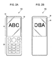
Fig. 2 is a diagram illustrating a transparent display, in whichFig. 2A is a front view of the terminal, andFig. 2B is a rear view thereof. -
Fig. 3 is a diagram illustrating a transverse unevenness as a light unevenness in the transparent display. -
Fig. 4 is a schematic diagram illustrating a light guide state in a light guide plate, which is thought as a factor of the transverse unevenness. -
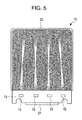
Fig. 5 is a diagram illustrating a longitudinal line as a light unevenness in the transparent display. -
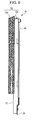
Fig. 6 is a diagram illustrating a light source unevenness as another light unevenness in the transparent display. -
Fig. 7 is a diagram illustrating a first embodiment of the present invention, in whichFig. 7A is a sectional view seen from the arrow VIIA-VIIA inFig. 7B, and Fig. 7B is a diagram where the step section side of the light guide plate is seen from the rear face. -
Figs. 8A and Fig. 8B are diagrams illustrating modifications of the first embodiment when there is a plurality of light sources. -
Fig. 9 is a diagram illustrating a second embodiment of the present invention, in whichFig. 9A is a sectional view seen from the arrow IXA-IXA inFig. 9B, and Fig. 9B is a diagram where the step section side of the light guide plate is seen from the rear face. -
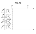
Fig. 10 is a diagram illustrating a modification of the second embodiment when there is a plurality of light sources. -
Fig. 11 is a diagram illustrating a third embodiment of the present invention, in whichFig. 11A is a sectional view seen from the arrow XIA-XIA inFig. 11B, and Fig. 11B is a diagram where the step section side of the light guide plate is seen from the rear face. -
Fig. 12 is a diagram illustrating a modification of the third embodiment when there is a plurality of light sources. -
Figs. 13A and Fig. 13B are diagrams illustrating a fourth embodiment of the present invention. -
Fig. 14A and Fig. 14B are diagrams illustrating a fifth embodiment of the present invention. -
Fig. 15 is a diagram illustrating a sixth embodiment of the present invention. - Exemplary embodiments of the present invention will now be described in detail with reference to the drawings.
-
Fig. 1 shows an appearance of aportable telephone terminal 100 which is an example of an electronic device according to an embodiment of the present invention.Fig. 1A is a perspective view where a front face side is seen, andFig. 1B is a perspective view where a rear face side is seen. - The portable telephone terminal (hereinafter, simply referred to as a "terminal") 100is a so-called straight type terminal, and is provided with a liquid crystal ("LC")
module 10 in the front face side of ahousing 30 and anoperation section 20 in its lower part. Alight guide plate 12, constituting a portion of theLC module 10, which is a transparent panel member, includes adisplay section 11 which constitutes a display image plane while overlapping an LC panel (not shown inFig. 1 ) placed in the back thereof. A material of thelight guide plate 12 may adopt, for example, synthetic resin such as acryl, or glass, or the like. Thelight guide plate 12 includes a step section 13 (hidden in the back of theoperation section 20 inFig. 1 ). Thisstep section 13 is connected to thedisplay section 11, and has a surface which is lower than an image plane position by one step. Thislight guide plate 12 guides light emitted from a light source described later, to the whole image plane, in this embodiment. - The LC panel of the terminal 100 has a
transparent window section 40 in the rear face area of the housing corresponding to thedisplay section 11. Thereby, there is a constitution of the transparent display which can make the other side seen through by passing through the display image plane, according to the display state of the LC panel placed in the back of thelight guide plate 12. The LC panel in this embodiment uses a polymer dispersed LC. Thewindow section 40 may be empty, or may be constituted by a transparent panel member like thelight guide plate 12. Although not shown in the figure, for example, when the image plane is seen in the state where a palm or fingers are put behind the terminal and the terminal is supported, the palm or the fingers are seen through gaps between images. - Also, as shown in
Figs. 2A and 2B , the image displayed on thedisplay section 1 placed on the surface side of the terminal 100 can be seen as a bilaterally symmetric mirror image from thewindow section 40 in the rear side. - Description of this embodiment will be made following description ol' various kinds of light unevenness, that is, a transverse unevenness, a longitudinal line, and a source light unevenness. This embodiment will be described in the premise of front light which illuminates the LC panel from the front face side of the LC panel. However, the present invention is also applicable to a case of a backlight which illuminates the LC panel from the rear face side of the LC panel.
-
Fig. 3 is a diagram illustrating a transverse unevenness as a kind of light unevenness in the transparent display. - As described above, a diffusion plate or the like which overlaps the display image plane may not be used in the transparent display. For this reason, if the entire display image plane performs, for example, a white solid display with the same brightness, even when the entire image plane of the
display section 11 is uniformly illuminated by the light from the light source in thelight guide plate 12, the transverse unevenness is generated as shown in the figure. A factor of the generation of this transverse unevenness lies in that since thelight guide plate 12 has a remarkably different structure, a part where the light is collected and a part where the light is not collected based on the reflection of light are generated. - An
element 21 shown inFig. 3 represents a flexible printed circuit board which gives signals for driving the LC panel. -
Fig. 4 shows a schematic light guide state in thelight guide plate 12, which is thought as the factor of the transverse unevenness. Thislight guide plate 12 is shown schematically for description, and shapes of its detailed parts or ratios of the respective parts are different from those in an actual one. As described above, theLC panel 14 is disposed in the back of thelight guide plate 12 of theLC module 10. Thelight guide plate 12 constituting a portion of theLC module 10, as described above, is connected to thedisplay section 11, and has thestep section 13 lower than the image plane position by one step. Alight source 15 is arranged inside thestep section 13. - In this embodiment, one or more light emitting diodes (LEDs) are used as the
light source 15. - As can be seen from
Fig. 4 , the light illuminated to thedisplay section 11 side from thelight source 15 inside thestep section 13 includes a direct light which directly reaches the surface of thedisplay section 11 in thelight guide plate 12, and a reflected light which reaches the surface through one or more reflections on the inner surfaces of the light guide plate. Thereby, as shown inFig. 3 , the amount of light is different in the position of the longitudinal direction of the display image plane. This is estimated as the factor of the transverse unevenness described above. - For example, the lower end part of the light guide plate surface close to the light source is not reached by the direct light from the light source but by the reflected light only, and thus is dark. In the
step section 13, a part which is reached by both the reflected light and the direct light is brighter than a part which is reached by the reflected light only. A part is also bright which is reached by the direct light and a light reflected from the upper end surface of the light guide plate. - An intensity of the reflected light is varied by the surface treatment of the upper end surface in the part which is reached by the direct light and the reflected light from the upper end surface of the light guide plate, and the part may be thereby brighter or darker than the part which is reached by both the reflected light and the direct light in the
step section 13. Actually, there are many light paths which undergo reflections several times, so it is not as simple as the above description. Anyway, as the factor of the transverse unevenness which is an issue of the present invention, the step difference in thelight guide plate 12 is believed to be a prime factor. -
Fig. 5 is a diagram illustrating a longitudinal line as another light unevenness in the transparent display. This longitudinal line is thought to be generated by the light, emitted from the respective light sources 15 (in this example, four light sources), directly reaching the surface of thelight guide plate 12. That is to say, the light emitted from the light sources may not be sufficiently diffused, and, in this state, the light travels in thelight guide plate 12, so this causes the longitudinal lines. Thelight guide plate 12 itself is transparent, and thus is not really contribute to the diffusion of the light. For this reason, as shown inFig. 5 , the light paths are seen as they are, and these form the light unevenness of the longitudinal lines. -
Fig. 6 is a diagram illustrating a source light unevenness as another light unevenness in the transparent display. This figure shows a side view of theLC module 10. Thelight guide plate 12 overlapping theLC panel 14 includes anouter magnifying section 12a and aninner installing section 12b. Themagnifying section 12a is a part which constitutes the display image plane. The installingsection 12b is a part for installing the housing 30 (that is, a housing part in the rear face side). In this embodiment, themagnifying section 12a and theinstalling section 12b are formed as a single body and are made of the same transparent material. The lower end side of theinstalling section 12b extends downwards further than the magnifyingsection 12a so as to form thestep section 13. - A factor of the source light unevenness is substantially the same as that of the longitudinal line described above. In other words, it is the factor for the light emitted from the light source to be directly seen in the lateral end surface without the sufficient diffusion of the light from the light source in the
light guide plate 12. If the lateral end surface of thelight guide plate 12 can be hidden, the light unevenness is not problematic any longer; however, like this embodiment, there is a case where the end surface of thelight guide plate 12 may not be hidden in terms of design. - The light unevenness is problematic in this case.
- As above, the light unevenness caused by various factors has much influence on the visual quality of the LCD, and it is needless to say that the entire image plane with uniform brightness is preferable.
- Methods that the transparent display is implemented and the light unevenness is reduced include a method that an optical analysis is made and patterns for diffusing light are added to the light guide plate which protects the LCD, and the like. The optical analysis costs a lot, and furthermore the transparency of the display device is much influenced by light diffusion.
- Planarization of the
light guide plate 12 by removal of the step from thelight guide plate 12 can solve the transverse unevenness. However, if the step difference is removed from thelight guide plate 12, the cabinet (the upper end of the member constituting the operation section in this example) for hiding the light source arranged in thestep section 13 protrudes forward further than the display surface, and thus a step happens oppositely in appearance of the terminal. - In addition, a method or the like is considered that the step of the
light guide plate 12 is removed, and a place desired to be hidden under thelight guide plate 12 is not hidden in the cabinet but is only colored. In this case, however, in terms of cost, or the necessity of accordance of colors with other parts, the method may be difficult to actually implement. - Hereinafter, diffusion mechanisms which diffuse light from the light source for improving the light unevenness will be described.
-
Fig. 7 is a diagram illustrating a first embodiment of the present invention.Fig. 7B is a diagram where thestep section 13 side of thelight guide plate 12 is seen from the rear face, andFig. 7A is a sectional view seen from the arrow VIIA-VIIA therein. In the example in the figure, an LED as thelight source 15 is disposed in aconcave section 16 provided in thestep section 13 of thelight guide plate 12, and at least aninner wall surface 17 on which the light is incident undergoes a surface texturing. The surface texturing refers to a processing where patterns are added to surfaces of processed materials, for example, a processing for adding minute asperity such as a leather pattern, tree texture, rock texture, sand texture, pearskin finish, cloth texture, geometric pattern or the like. A method can be also considered that a diffusion plate is attached to the associated wall surface. However, in consideration of cost of the diffusion plate, or misalignment at the time of the attachment, it is favorable to directly process a surface of a material such as acryl or the like so as to be formed with the member as a single body. The light emitted from thelight source 15 is incident on the wall surface where the surface texturing is performed, and thereby the incident light can be diffused. Although theconcave section 16 is formed in the rear face side of thelight guide plate 12 in this embodiment, it may be formed in the front face side thereof. Alternatively, a through-hole which penetrates through the light guide plate from the front face side to the rear face side is also good. In the case of theconcave section 16 formed in the front face side, or the through-hole, a light blocking component is independently formed in the front face side. -
Figs. 8A and 8B show modifications of the first embodiment when there is a plurality of light sources. The example inFig. 8A shows that a plurality ofconcave sections 16 are formed one to one with respect to the plurality of light sources 15 (four light sources in this example). The example inFig. 8B shows that a singleconcave portion 16 is shared with the plurality oflight sources 15. -
Fig. 9 is a diagram illustrating a second embodiment of the present invention this example, an LED as thelight source 15 is disposed in aconcave section 16 provided in thestep section 13 of thetransparent panel member 12, and at least aninner wall surface 18 on which the light is incident is curved with a shape protruding toward thelight source 15. Alternatively, it may be curved with a shape retreating from thelight source 15. The light emitted from thelight source 15 is incident on this curved wall surface, and thus the incident light can be diffused. -
Fig. 10 shows a modification of the second embodiment when there is a plurality of light sources. In this example, a plurality ofconcave sections 16 are formed one to one with respect to a plurality oflight sources 15. -
Fig. 11 is a diagram illustrating a third embodiment of the present invention.Fig. 11B is a diagram where thestep section 13 side of thelight guide plate 12 is seen from the rear face, andFig. 11A is a sectional view seen from the arrow XIA-XIA therein. In this example, acylindrical cavity 19 forming a cylindrical boundary face is arranged in front of theconcave section 16 of thestep section 13, in a direction of the light emitted from thelight source 15 disposed therein. The light from thelight source 15 is incident on this cylindrical boundary face, and thus the incident light can be diffused. -
Fig. 12 shows a modification of the third embodiment when there is a plurality of light sources. In this example, thecylindrical cavities 19 are arranged in front of the plurality oflight sources 15, respectively. -
Fig. 13 is a diagram illustrating a fourth embodiment of the present invention. In this embodiment, a plurality oflight sources 15 are disposed in a plurality ofconcave sections 16 provided in the step section, respectively, and directions of light emitted from the plurality oflight sources 15 are different from each other. Thereby, the light from thelight sources 15 can be diffused. Also, in this configuration, the directions of the light emitted from the plurality oflight sources 15 are directions other than a direction directing to the display section. The arrangement of the plurality oflight sources 15 and the emitted directions of the light are bilaterally symmetric. For example, if a direction originally directing to thedisplay section 11 is taken as a reference (0 degrees), of fourlight sources 15 in this embodiment, twoinner light sources 15 are tilted outwards by 90 degrees, and two outerlight sources 15 are tilted inwards by 135 degrees. - Thereby, it can be achieved that the brightness in the transverse direction can be balanced as well as the light from the
light sources 15 can be diffused. - In this configuration, an opaque diffusion plate may not be sufficiently used in implementing the transparent display, and thus the light unevenness is reduced at the expense of the amount of light to some degree.
-
Fig. 14 is a diagram illustrating a fifth embodiment of the present invention. In the example shown inFig. 14A , anR section 11a as a diffusion mechanism is formed through an R processing at a place where thestep section 13 of thelight guide plate 12 begins to erect toward thedisplay section 11. The length L1 of thedisplay section 11 in the longitudinal direction and the length L2 from thelight source 15 to the erecting edge are the same as those of the case where theR section 11a is not present. This configuration enables the light from thelight source 15 to be easily guided to thelower end part 25 of thedisplay section 11. Thereby, the transverse unevenness described inFig. 3 is improved. Thelight source 15 is arranged so as to be close to thedisplay section 11, resulting in increasing the amount of light reaching the lower part of the image plane. However, if thelight source 15 is not to be directly seen from the appearance surface (display image plane), the length L2 may be more than a certain distance. Therefore, a position of thelight source 15 may be preferably defined in consideration of both conditions. - In the example shown in
Fig. 14B , in addition to theR section 11a anR section 11b is also formed at a place where thestep section 13 of thelight guide plate 12 finishes erecting toward thedisplay section 11. -
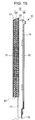
Fig. 15 is a diagram illustrating a sixth embodiment of the present invention. The above-described surface texturing is performed for the inner wall of the concave section where the light source is disposed; however, it may be performed for parts other than the display section surface of thelight guide plate 12 and its back (that is, parts causing no difficulty in displaying as the transparent display). These parts may include, for example, the upper end surfaces U1 and U2 of thelight guide plate 12, its lateral end surfaces S1 and S2, and its lower end surfaces B1 and B2. - The light from the light source is diffused by these diffusion mechanisms, and thereby the above-described various kinds of light unevenness can be reduced.
- As such, although the preferred embodiments of the present invention have been described, various modifications and alterations are possible in addition to the embodiments described above. For example, the above-described embodiments and modifications may adopt possible combinations of two or more arbitrary ones. For example, the surface texturing may be performed for the
curved section 18 shown inFig. 9 , or for the wall surface of thecylindrical cavity 19 shown inFig. 11 . Thecylindrical cavity 19 shown inFig. 11 may be provided in the display section side of theconcave sections 16 inFigs. 7 and9 . The R section shown inFig. 14 may be used along with all the other embodiments. The configuration shown inFig. 15 may be also used along with all the other embodiments. - Although, in only the configuration of the
concave section 16, its whole periphery has been surrounded by the inner wall, a portion thereof may be open to outside. - The portable telephone terminal has been exemplified by the so-called straight type only; however, the present invention is applicable to a folder type or a slide type terminal constituted by an upper housing and a lower housing. In this case, one housing (for example, the upper housing) may be provided with the transparent display.
- The present application contains subject matter related to that disclosed in Japanese Priority Patent Application
JP 2009-259506 - It should be understood by those skilled in the art that various modifications, combinations, sub-combinations and alterations may occur depending on design requirements and other factors insofar as they are within the scope of the appended claims.
- In so far as the embodiments of the invention described above are implemented, at least in part, using software-controlled data processing apparatus, it will be appreciated that a computer program providing such software control and a transmission, storage or other medium by which such a computer program is provided are envisaged as aspects of the present invention.
Claims (12)
- A liquid crystal module, comprising:a liquid crystal panel;a transparent panel member configured to include a display section constituting a display image plane while overlapping the liquid crystal panel, and a step section connected to the display section and lower than an image plane position by one step;at least one light source disposed in the step section of the transparent panel member; anda diffusion mechanism provided in a part other than the display image plane of the display section and a face opposite thereto, and diffusing light from the light source.
- The liquid crystal module according to Claim 1, wherein the light source is disposed in a concave section provided in the step section, and the diffusion mechanism includes that a surface texturing is performed for at least a face of the concave section where light from the light source is incident.
- The liquid crystal module according to Claim 1 or 2, wherein the light source is disposed in a concave section provided in the step section, and the diffusion mechanism includes that at least a face of the concave section where light from the light source is incident is curved.
- The liquid crystal module according to any one of Claims 1 to 3, wherein the diffusion mechanism includes that the surface texturing is performed for at least one lateral face of the display section of the transparent panel member.
- The liquid crystal module, according to any one of Claims 1 to 4, wherein a plurality of light sources as the light source is disposed in a plurality of concave sections provided in the step section, respectively, and, the diffusion mechanism includes that directions of light emitted from the plurality of light sources are different from each other.
- The liquid crystal module according to Claim 5, wherein the directions of light emitted from the plurality of light sources are directions other than a direction directing to the display section.
- The liquid crystal module according to Claim 5 or 6, wherein the arrangement of the plurality of light sources and the emitted directions of light are bilaterally symmetric.
- The liquid crystal module according to any one of Claims 1 to 7, wherein the light source is disposed in a concave section provided in the step section, and the diffusion mechanism includes that at least a cylindrical boundary face is formed in front of the concave section in at least a direction of light emitted from the light source.
- The liquid crystal module according to any one of Claims 1 to 8, wherein the diffusion mechanism includes that an R section is formed at a place where the step section of the transparent panel member begins to erect toward the display section.
- The liquid crystal module according to Claim 9, wherein the diffusion mechanism further includes that an R section is formed at a place where the step section of the transparent panel member finishes erecting toward the display section.
- The liquid crystal module according to any one of Claims 1 to 10, wherein the liquid crystal panel adopts a polymer dispersed liquid crystal.
- An electronic device using the liquid crystal module as a display device according to any one of Claims 1 to 11, comprising a rear face area of a housing, corresponding to the display section, transparent or empty.
Applications Claiming Priority (1)
| Application Number | Priority Date | Filing Date | Title |
|---|---|---|---|
| JP2009259506A JP2011107229A (en) | 2009-11-13 | 2009-11-13 | Liquid crystal module and electronic equipment |
Publications (1)
| Publication Number | Publication Date |
|---|---|
| EP2333605A1 true EP2333605A1 (en) | 2011-06-15 |
Family
ID=43477999
Family Applications (1)
| Application Number | Title | Priority Date | Filing Date |
|---|---|---|---|
| EP10167415A Withdrawn EP2333605A1 (en) | 2009-11-13 | 2010-06-25 | Liquid crystal module and electronic device |
Country Status (3)
| Country | Link |
|---|---|
| US (1) | US8279373B2 (en) |
| EP (1) | EP2333605A1 (en) |
| JP (1) | JP2011107229A (en) |
Families Citing this family (10)
| Publication number | Priority date | Publication date | Assignee | Title |
|---|---|---|---|---|
| KR101824036B1 (en) * | 2011-06-30 | 2018-03-14 | 엘지이노텍 주식회사 | backlight unit and display apparatus using the same |
| JP6089271B2 (en) * | 2012-12-13 | 2017-03-08 | パナソニックIpマネジメント株式会社 | Lighting device |
| WO2016021442A1 (en) * | 2014-08-06 | 2016-02-11 | 国立大学法人東京農工大学 | Display device |
| US10637977B1 (en) * | 2016-08-31 | 2020-04-28 | Apple Inc. | Illumination systems for items with leather |
| KR102487190B1 (en) * | 2017-12-12 | 2023-01-10 | 현대자동차 주식회사 | Light spreading complex lens |
| JP7467688B2 (en) | 2021-01-21 | 2024-04-15 | 株式会社ジャパンディスプレイ | Display device |
| JP7505044B2 (en) | 2021-01-21 | 2024-06-24 | 株式会社ジャパンディスプレイ | Display device |
| JP7566689B2 (en) | 2021-05-11 | 2024-10-15 | 株式会社ジャパンディスプレイ | Display device |
| JP2024078136A (en) | 2022-11-29 | 2024-06-10 | 株式会社ジャパンディスプレイ | Display device and cover glass |
| JP2024077811A (en) | 2022-11-29 | 2024-06-10 | 株式会社ジャパンディスプレイ | Display device |
Citations (7)
| Publication number | Priority date | Publication date | Assignee | Title |
|---|---|---|---|---|
| JPH05100118A (en) | 1991-10-04 | 1993-04-23 | Kimoto & Co Ltd | Light transmission plate for planar light source |
| US20030063235A1 (en) * | 2001-09-07 | 2003-04-03 | Rohm Co., Ltd. | Liquid crystal display with lighting unit for uniform irradiation of liquid crystal panel |
| US20030099116A1 (en) * | 2001-11-26 | 2003-05-29 | Nokia Corporation | Illumination system for an electronic device |
| US20040212981A1 (en) * | 2003-04-28 | 2004-10-28 | Toppoly Optoelectronics Corp. | LED lighting module |
| EP1510994A1 (en) * | 2003-08-21 | 2005-03-02 | Pioneer Corporation | Display system and electronic appliance including the display |
| EP1832806A1 (en) * | 2004-12-27 | 2007-09-12 | Nichia Corporation | Light guide and surface emitting device using same |
| US20090256996A1 (en) * | 2008-04-11 | 2009-10-15 | Sony Corporation | Light guide plate, display device, and electronic apparatus with display |
-
2009
- 2009-11-13 JP JP2009259506A patent/JP2011107229A/en not_active Withdrawn
-
2010
- 2010-06-23 US US12/821,474 patent/US8279373B2/en not_active Expired - Fee Related
- 2010-06-25 EP EP10167415A patent/EP2333605A1/en not_active Withdrawn
Patent Citations (7)
| Publication number | Priority date | Publication date | Assignee | Title |
|---|---|---|---|---|
| JPH05100118A (en) | 1991-10-04 | 1993-04-23 | Kimoto & Co Ltd | Light transmission plate for planar light source |
| US20030063235A1 (en) * | 2001-09-07 | 2003-04-03 | Rohm Co., Ltd. | Liquid crystal display with lighting unit for uniform irradiation of liquid crystal panel |
| US20030099116A1 (en) * | 2001-11-26 | 2003-05-29 | Nokia Corporation | Illumination system for an electronic device |
| US20040212981A1 (en) * | 2003-04-28 | 2004-10-28 | Toppoly Optoelectronics Corp. | LED lighting module |
| EP1510994A1 (en) * | 2003-08-21 | 2005-03-02 | Pioneer Corporation | Display system and electronic appliance including the display |
| EP1832806A1 (en) * | 2004-12-27 | 2007-09-12 | Nichia Corporation | Light guide and surface emitting device using same |
| US20090256996A1 (en) * | 2008-04-11 | 2009-10-15 | Sony Corporation | Light guide plate, display device, and electronic apparatus with display |
Also Published As
| Publication number | Publication date |
|---|---|
| US20110116013A1 (en) | 2011-05-19 |
| US8279373B2 (en) | 2012-10-02 |
| JP2011107229A (en) | 2011-06-02 |
Similar Documents
| Publication | Publication Date | Title |
|---|---|---|
| US8279373B2 (en) | Liquid crystal module and electronic device | |
| CN103293764B (en) | There is the electronic equipment of the sign structure being illuminated | |
| US8287370B2 (en) | Liquid crystal display unit, game device and display method for use in liquid crystal display unit | |
| JP4870364B2 (en) | Backlight device for wrist watch information display element | |
| CN209690674U (en) | Direct-lit backlight module and display device | |
| KR101400285B1 (en) | Front light unit and flat display apparatus employing the same | |
| US9927567B2 (en) | Display with additional lighting effects | |
| KR20100097515A (en) | Backlight unit for liquid crystal display device module | |
| EP2388513A1 (en) | Light module | |
| CN108388048B (en) | Backlight module and display device | |
| KR20040014367A (en) | Liquid crystal display device | |
| US20050185422A1 (en) | Backlighting device for an information display element of a portable object | |
| KR20190104852A (en) | A Edge-emitting type display device and game device having the same | |
| CN103732973A (en) | Lighting device and display device provided with same | |
| JP5600998B2 (en) | Laminated sheet for information display panel, information display panel, and information display device | |
| CN208421475U (en) | Backlight module, liquid crystal display die set and electronic device | |
| WO2012115993A1 (en) | Display front lighting device | |
| CN208421474U (en) | Backlight module, liquid crystal display die set and electronic device | |
| EP4470838A1 (en) | Lighting system for a vehicle | |
| CN103339476A (en) | monitor | |
| EP3745692B1 (en) | Led light source mechanism, telephone set, and method for forming led light source | |
| CN121634605A (en) | Display device | |
| KR20190043909A (en) | Display apparatus | |
| CN107577007B (en) | Display device for vehicle | |
| KR102068139B1 (en) | Prism sheet, back light unit and display device comprising the same |
Legal Events
| Date | Code | Title | Description |
|---|---|---|---|
| PUAI | Public reference made under article 153(3) epc to a published international application that has entered the european phase |
Free format text: ORIGINAL CODE: 0009012 |
|
| AK | Designated contracting states |
Kind code of ref document: A1 Designated state(s): AL AT BE BG CH CY CZ DE DK EE ES FI FR GB GR HR HU IE IS IT LI LT LU LV MC MK MT NL NO PL PT RO SE SI SK SM TR |
|
| AX | Request for extension of the european patent |
Extension state: BA ME RS |
|
| 17P | Request for examination filed |
Effective date: 20100629 |
|
| RAP1 | Party data changed (applicant data changed or rights of an application transferred) |
Owner name: SONY MOBILE COMMUNICATIONS AB |
|
| 17Q | First examination report despatched |
Effective date: 20160203 |
|
| STAA | Information on the status of an ep patent application or granted ep patent |
Free format text: STATUS: EXAMINATION IS IN PROGRESS |
|
| STAA | Information on the status of an ep patent application or granted ep patent |
Free format text: STATUS: THE APPLICATION IS DEEMED TO BE WITHDRAWN |
|
| 18D | Application deemed to be withdrawn |
Effective date: 20180905 |