EP2330497A1 - Flat panel display integrated with touch screen panel - Google Patents
Flat panel display integrated with touch screen panel Download PDFInfo
- Publication number
- EP2330497A1 EP2330497A1 EP10177766A EP10177766A EP2330497A1 EP 2330497 A1 EP2330497 A1 EP 2330497A1 EP 10177766 A EP10177766 A EP 10177766A EP 10177766 A EP10177766 A EP 10177766A EP 2330497 A1 EP2330497 A1 EP 2330497A1
- Authority
- EP
- European Patent Office
- Prior art keywords
- upper substrate
- transparent conductive
- region
- sealing material
- flat panel
- Prior art date
- Legal status (The legal status is an assumption and is not a legal conclusion. Google has not performed a legal analysis and makes no representation as to the accuracy of the status listed.)
- Granted
Links
Images

Classifications
-
- G—PHYSICS
- G06—COMPUTING OR CALCULATING; COUNTING
- G06F—ELECTRIC DIGITAL DATA PROCESSING
- G06F3/00—Input arrangements for transferring data to be processed into a form capable of being handled by the computer; Output arrangements for transferring data from processing unit to output unit, e.g. interface arrangements
- G06F3/01—Input arrangements or combined input and output arrangements for interaction between user and computer
- G06F3/03—Arrangements for converting the position or the displacement of a member into a coded form
- G06F3/041—Digitisers, e.g. for touch screens or touch pads, characterised by the transducing means
- G06F3/044—Digitisers, e.g. for touch screens or touch pads, characterised by the transducing means by capacitive means
-
- G—PHYSICS
- G06—COMPUTING OR CALCULATING; COUNTING
- G06F—ELECTRIC DIGITAL DATA PROCESSING
- G06F3/00—Input arrangements for transferring data to be processed into a form capable of being handled by the computer; Output arrangements for transferring data from processing unit to output unit, e.g. interface arrangements
- G06F3/01—Input arrangements or combined input and output arrangements for interaction between user and computer
- G06F3/03—Arrangements for converting the position or the displacement of a member into a coded form
- G06F3/041—Digitisers, e.g. for touch screens or touch pads, characterised by the transducing means
- G06F3/0412—Digitisers structurally integrated in a display
-
- G—PHYSICS
- G06—COMPUTING OR CALCULATING; COUNTING
- G06F—ELECTRIC DIGITAL DATA PROCESSING
- G06F3/00—Input arrangements for transferring data to be processed into a form capable of being handled by the computer; Output arrangements for transferring data from processing unit to output unit, e.g. interface arrangements
- G06F3/01—Input arrangements or combined input and output arrangements for interaction between user and computer
- G06F3/03—Arrangements for converting the position or the displacement of a member into a coded form
- G06F3/041—Digitisers, e.g. for touch screens or touch pads, characterised by the transducing means
- G06F3/044—Digitisers, e.g. for touch screens or touch pads, characterised by the transducing means by capacitive means
- G06F3/0446—Digitisers, e.g. for touch screens or touch pads, characterised by the transducing means by capacitive means using a grid-like structure of electrodes in at least two directions, e.g. using row and column electrodes
-
- G—PHYSICS
- G06—COMPUTING OR CALCULATING; COUNTING
- G06F—ELECTRIC DIGITAL DATA PROCESSING
- G06F2203/00—Indexing scheme relating to G06F3/00 - G06F3/048
- G06F2203/041—Indexing scheme relating to G06F3/041 - G06F3/045
- G06F2203/04103—Manufacturing, i.e. details related to manufacturing processes specially suited for touch sensitive devices
-
- G—PHYSICS
- G06—COMPUTING OR CALCULATING; COUNTING
- G06F—ELECTRIC DIGITAL DATA PROCESSING
- G06F2203/00—Indexing scheme relating to G06F3/00 - G06F3/048
- G06F2203/041—Indexing scheme relating to G06F3/041 - G06F3/045
- G06F2203/04111—Cross over in capacitive digitiser, i.e. details of structures for connecting electrodes of the sensing pattern where the connections cross each other, e.g. bridge structures comprising an insulating layer, or vias through substrate
Definitions
- Example embodiments relate to a flat panel display (FPD). More particularly, example embodiments relate to an FPD integrated with a touch screen panel.
- FPD flat panel display
- a touch screen panel is an input device on a screen, e.g., on an image display device, for selecting instruction/command content, e.g., by a human hand or an object, of a user.
- a conventional touch screen panel may be provided on a front surface of the image display device to convert a contact position, e.g., of a human hand or an object, into an electrical signal. Therefore, the instruction content selected by the contact position may be received by the image display device as an input signal.
- the touch screen panel may replace an additional input device coupled to the image display device, e.g., to operate a keyboard and/or a mouse.
- the touch screen panel may be realized by several methods, e.g., a resistance layer method, an optical sensing method, and an electrostatic capacitance method.
- a touch screen panel realized by the electrostatic capacitance method may sense a change in the electrostatic capacitance formed by a conductive sensing pattern and a peripheral sensing pattern or a ground electrode, when the touch screen panel is contacted to generate the electrical signal.
- the touch screen panel may be attached to a front surface of a FPD, e.g., a liquid crystal display (LCD), an organic light emitting diode (OLED) display, etc.
- a FPD liquid crystal display
- OLED organic light emitting diode
- Embodiments are directed to a FPD integrated with a touch screen panel, which substantially overcome one or more of the problems due to the limitations and disadvantages of the related art.
- FPC flexible printed circuit
- a FPD integrated with a touch screen panel including an upper substrate and a lower substrate facing each other, the upper substrate including a display region and first and second non-display regions surrounding the display region, a plurality of sensing patterns on the display region of the upper substrate, a plurality of sensing lines on the first non-display region of the upper substrate, a sealing material on the second non-display region of the upper substrate, the sealing material connecting the upper and lower substrates, and a flexible printed circuit (FPC) bonding pad unit on the second non-display region of the upper substrate, the FPC bonding pad unit including a plurality of bonding pads coupled to the plurality of sensing lines, the bonding pads including a transparent conductive material in regions overlapping the sealing material.
- FPC flexible printed circuit
- a transparent conductive material in the sense of the present invention is preferably a material having a maximum optical transmittance (ratio of intensity of light transmitted through the transparent conductive material and intensity of light irradiated onto the transparent conductive material for a thickness of the transparent conductive material being equal to the thickness of the bonding pad) for visible light of preferably more than 20%, more preferably more than 30%, more preferably more than 40%, more preferably more than 50%, more preferably more than 60%, more preferably more than 70%, more preferably more than 80% and still more preferably more than 90%.
- a maximum optical transmittance ratio of intensity of light transmitted through the transparent conductive material and intensity of light irradiated onto the transparent conductive material for a thickness of the transparent conductive material being equal to the thickness of the bonding pad
- the upper substrate has a maximum optical transmittance (ratio of intensity of light transmitted through the upper substrate and intensity of light irradiated onto the upper substrate) for visible light of preferably more than 50%, more preferably more than 60%, more preferably more than 70%, more preferably more than 80%, more preferably more than 90% and still more preferably more than 95%.
- a maximum optical transmittance ratio of intensity of light transmitted through the upper substrate and intensity of light irradiated onto the upper substrate for visible light of preferably more than 50%, more preferably more than 60%, more preferably more than 70%, more preferably more than 80%, more preferably more than 90% and still more preferably more than 95%.
- a transparent conductive material in the sense of the present invention is preferably a material having an electrical conductivity of preferably more than 10 2 S/m, more preferably of more than 10 3 S/m, more preferably of more than 10 4 S/m, more preferably of more than 10 5 S/m an still more preferably of more than 10 6 S/m.
- the electrical conductivity transparent conductive material is smaller than 80*10 6 S/m, more preferably smaller than 60*10 6 S/m, more preferably smaller than 40*10 6 S/m an still more preferably smaller than 20*10 6 S/m.
- the electrical conductivity transparent conductive material is selected from the group consisting of ITO, AlZnO, IZnO, GaZnO, PEDOT:PSS (Polyethylenedioxythiophene-Polystyrenesulfonate),
- the bonding pads of the FPC bonding pad unit may include a first region that overlaps the sealing material and a second region that does not overlap the sealing material, the structures of the first region and the second region being different from each other.
- the first region of the bonding pad may include a first insulating layer formed on the second non-display region of the upper substrate so that a predetermined region is opened, a transparent conductive pattern formed to include the opened region, and a second insulating layer in which a region that overlaps the transparent conductive pattern is opened so that the transparent conductive pattern is exposed.
- the transparent conductive pattern and the sensing patterns include a substantially same material.
- the FPD further comprises island-shaped opaque metal patterns under the transparent conductive pattern.
- the FPD further comprises slit-shaped opaque metal patterns under the transparent conductive pattern.
- the second region of the bonding pad may include an opaque metal pattern formed on the second non-display region of the upper substrate, a first insulating layer in which a region that overlaps the opaque metal pattern is opened so that the opaque metal pattern is exposed, a transparent conductive pattern formed in a region that overlaps the exposed opaque metal pattern, and a second insulating layer in which a region that overlaps the transparent conductive pattern is opened so that the transparent conductive pattern is exposed.
- the opaque metal pattern is made of the same material as the sensing lines.
- the opaque metal pattern has a maximum optical transmittance (ratio of intensity of light transmitted through the opaque metal pattern and intensity of light irradiated onto the opaque metal pattern) for visible light of preferably less than 50%, more preferably less than 40%, more preferably less than 30%, more preferably less than 20%, more preferably less than 10% and still more preferably less than 5%.
- a maximum optical transmittance ratio of intensity of light transmitted through the opaque metal pattern and intensity of light irradiated onto the opaque metal pattern for visible light of preferably less than 50%, more preferably less than 40%, more preferably less than 30%, more preferably less than 20%, more preferably less than 10% and still more preferably less than 5%.
- the opaque metal pattern may be separated from the sealing material by a predetermined distance.
- the predetermined distance ranges between 20 to 200 ⁇ m, more preferably between 40 to 160 ⁇ m, more preferably between 60 to 140 ⁇ m and still more preferably between 80 to 120 ⁇ m. Still more preferably, the predetermined distance may be 100 ⁇ m. According to the ranges of the preferred predetermined distance it is possible to ensure sufficient conductivity on the one hand and to simultaneously ensure sufficient transmission of the laser radiation for hardening the sealing on the other hand.
- Island-shaped opaque metal patterns may be further formed under the transparent conductive pattern.
- Slit-shaped opaque metal patterns may be further formed under the transparent conductive pattern.
- ratio of the surface area covered by the island-shaped opaque metal patterns/ slit-shaped opaque metal patterns and the surface area covered by transparent conductive pattern (in the first region) ranges from 0.05 to 0.95, more preferably from 0.10 to 0.90, more preferably from 0.15 to 0.85, more preferably from 0.20 to 0.80, more preferably from 0.25 to 0.75, more preferably from 0.30 to 0.70, more preferably from 0.35 to 0.65, more preferably from 0.40 to 0.60 and still more preferably from 0.45 to 0.55.
- the ranges of the preferred ratio of the surface area covered by the island-shaped opaque metal patterns/ slit-shaped opaque metal patterns and the surface area covered by transparent conductive pattern it is possible to ensure sufficient conductivity on the one hand and to simultaneously ensure sufficient transmission of the laser radiation for hardening the sealing on the other hand.
- Portions of the bonding pads overlapping the sealing material may include only the transparent conductive material.
- the sensing lines may be coupled to the bonding pads via opaque metal patterns, the metal patterns being positioned not to overlap the sealing material.
- the sensing lines may be coupled to the bonding pads via metal patterns, the bonding pads extending along a first direction, and the metal patterns being spaced apart from the sealing material along the first direction. Portions of the bonding pads overlapping the sealing material and including the transparent conductive material may be directly on the upper substrate.
- the sensing patterns may include X sensing patterns and Y sensing patterns formed in different layers.
- the X sensing patterns may be patterned to be coupled to each other in a first direction and the Y sensing patterns may be patterned to be coupled to each other in a second direction that intersects the first direction.
- the transparent conductive material of the bonding pads is configured to transmit laser light irradiation therethrough toward the sealing material.
- the transparent conductive material of the bonding pads may be configured to transmit laser light irradiation therethrough, so the sealing material may be melted by radiating laser light, and the melted sealing material may be hardened so that the upper substrate and the lower substrate are attached to each other.
- a method for manufacturing a flat panel display comprising: providing a flat panel display as disclosed in the present invention, providing sealing material between the upper substrate and the lower substrate, irradiating laser light onto the second non-display region through the upper substrate to harden the sealing material thereby attaching the upper substrate and the lower substrate to each other.
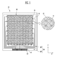
- FIG. 1 illustrates a plan view of an upper substrate of a FPD according to an embodiment
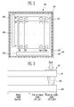
- FIG. 2 illustrates a plan view of a lower substrate of the FPD of FIG. 1 ;
- FIG. 3 illustrates a cross-sectional view of a partial region of a FPD according to an embodiment
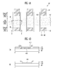
- FIG. 4A illustrates an enlarged plan view of a FPC bonding pad unit according to an embodiment
- FIG. 4B illustrates cross-sectional views along lines I-I' and II-II' of FIG. 4A ;
- FIGS. 5A and 5B illustrate enlarged plan views of a FPC bonding pad unit according to other embodiments.
- FIG. 1 illustrates a plan view of an upper substrate of a FPD according to an embodiment
- FIG. 2 illustrates a plan view of a lower substrate of the FPD in FIG. 1
- FIG. 3 illustrates a partial cross-sectional view of a connection between the upper and lower substrates of the FPD in FIG. 1 .
- a FPD may include a lower substrate 100 and an upper substrate 10 connected to each other via a sealing material 140.
- a touch screen panel may be formed on, e.g., directly on, the upper substrate 10 of the FPD.
- the FPD may be, e.g., an OLED display or a LCD.
- the upper substrate 10 may be an encapsulation substrate of the OLED display, and may be made of a transparent material, e.g., a glass substrate.
- the touch screen panel may include a plurality of sensing patterns 12 and 14 on the upper substrate 10, i.e., the encapsulation substrate. As further illustrated in FIG. 1 , the touch screen panel may include metal pads 15 electrically coupled to the sensing patterns 12 and 14, and sensing lines 16.
- the touch screen panel may be attached to the upper substrate 10 to overlap a display region 20 of the upper substrate 10. That is, the plurality of sensing patterns 12 and 14 may be formed on the display region 20 of the upper substrate 10, i.e., a region in which an image is displayed to detect a touch position.
- the metal pads 15 and the sensing lines 16 electrically coupled to the sensing patterns 12 and 14 may be formed in a non-display region 30 of the upper substrate 10.
- the non-display region 30 may be peripheral to the display region 20, e.g., the non-display region 30 may surround the display region 20.
- the non-display region 30 may be divided into a first non-display region 30', i.e., a region in which the metal pads 15 and the sensing lines 16 are formed, and a second non-display region 30", i.e., a region in which a FPC bonding pad unit 40 is formed.
- the second non-display region 30" may surround, e.g., completely surround, the first non-display region 30', so the first non-display region 30' may be between the display region 20 and the second non-display region 30".
- the FPC bonding pad unit 40 in the second non-display unit 30" may include a plurality of bonding pads 42 coupled to the sensing lines 16, and will be described in more detail below with reference to FIGS. 4A and 4B .
- the second non-display region 30" of the upper substrate 10 may be coated with the sealing material 140 ( FIG. 3 ), so the sealing material 140 may be formed between the upper substrate 10 and the lower substrate 100 in order to attach the upper substrate 10 and the lower substrate 100 of the FPD to each other.
- Laser light may be irradiated onto the second non-display region 30", so that the sealing material 140 may be hardened to attach the upper substrate 10 and the lower substrate 100 to each other.
- the plurality of sensing patterns 12 and 14 formed in the display region 20 may be alternately arranged to include X sensing patterns 12 and Y sensing patterns 14 coupled to each other. That is, the X sensing patterns 12 may be connected in units of columns having the same X coordinates, and the Y sensing patterns 14 may be connected in units of rows having the same Y coordinates. It is noted that “sensing patterns 12 and 14" and “X and Y sensing patterns 12 and 14" will be used hereinafter interchangeably.
- the X sensing patterns 12 may include a plurality of patterns arranged in columns, so the patterns within each column may have the same X coordinate and may be coupled to each other in a first direction (column direction).
- the Y sensing patterns 14 may include a plurality of patterns arranged in rows, so the patterns in each row may have the same Y coordinate and may be coupled to each other in a second direction (row direction).
- the X and Y sensing patterns 12 and 14 may be formed in different layers with an insulating layer (not shown) interposed therebetween.
- the X sensing patterns 12 may be patterned to be coupled to each other in the first direction
- the Y sensing patterns 14 may be patterned to be coupled to each other in the second direction. Therefore, a process of forming additional contact holes and coupling patterns may be omitted, so that the number of masks may be reduced and processes may be simplified.
- Example embodiments are not limited to the above.
- the X and Y sensing patterns 12 and 14 may be formed in the same layer, e.g., both the X and Y sensing patterns 12 and 14 may be formed directly on the upper substrate 10.
- a first portion of the X and Y sensing patterns 12 and 14 may be coupled to each other in a first direction in the patterning process, and a second portion of the X and Y sensing patterns 12 and 14, i.e., the remaining sensing patterns, may be coupled to each other in the second direction.
- the metal pads 15 of the touch screen panel may be arranged at an edge of the display region 20 where the X and Y sensing patterns 12 and 14 are formed. That is, the metal pads 15 may be at an inner edge of the first non-display region 30', e.g., at a boundary line between the display region 20 and the first non-display region 30', to couple the X and Y sensing patterns 12 and 14 to the plurality of sensing lines 16 formed on the first non-display region 30'.
- the metal pads 15 may electrically couple the X and Y sensing patterns 12 and 14 in units of one column or row to the sensing lines 16, so that a contact sensing signal may be supplied to a driving circuit for driving the touch screen panel.
- the metal pads 15 may electrically couple the X sensing patterns 12 in units of one column to the sensing lines 16, and may electrically couple the Y sensing patterns 14 in units of one row to the sensing lines 16.
- the sensing lines 16 may be coupled to the X and Y sensing patterns 12 and 14 through the metal pads 15 to couple the X and Y sensing patterns 12 and 14 to a driving circuit (not shown).
- the metal pads 15 and the sensing lines 16 may be made of a low resistance opaque metal material.
- the touch screen panel may be coupled to a FPC (not shown), on which an external driving circuit (not shown) may be mounted through the FPC bonding pad unit 40.
- the sensing lines 16 may be coupled between the FPC bonding pad unit 40 and the sensing patterns 12 and 14.
- a change in the electrostatic capacitance in accordance with the contact position may be transmitted from the X and Y sensing patterns 12 and 14 to the driving circuit via the metal pads 15 and the sensing lines 16. Then, a change in the electrostatic capacitance may be converted into an electrical signal by X and Y input processing circuits (not shown), so that the contact position may be detected and/or registered.
- the lower substrate 100 corresponding to the upper substrate 10 may include a display region 110 with pixels 112 and a non-display region 120.
- Each of the pixels 112 in the display region 110 may include an OLED having a first electrode, at least one organic layer, and a second electrode.
- the non-display region 120 may be formed to surround the display region 110.
- the non-display region 120 may be divided into a first non-display region 120', i.e., a region including a data driving circuit 132 and a scan driving circuit 130 for driving the plurality of pixels 112, formed on the display region 110 and a second non-display region 120" surrounding the first non-display region 120', i.e., a region including the sealing material 140 for attaching the lower substrate 100 to the upper substrate 10.
- the display region 110 and the first and second non-display regions 120' and 120" of the lower substrate 100 may correspond to, e.g., overlap with, or have the same size as, the display region 20 and the first and second non-display regions 30' and 30" of the upper substrate 10, respectively.
- the display region 110 may include a plurality of scan lines S1 to Sn arranged in a row direction, and a plurality of data lines D1 to Dm arranged in a column direction.
- each of the plurality of pixels 112 receiving signals from the scan and data driving circuits 130 and 132 may be formed to be connected to a respective scan line of the scan lines S1 to Sn and a respective data line of the data lines D1 to Dm.
- the scan and data driving circuits 130 and 132 may be formed. Further, metal wiring lines electrically coupled to the scan lines S 1 to Sn and the data lines D1 to Dm of the display region 110 may be formed. It is noted that “driving circuits” may refer to the data driving circuit 132 and the scan driving circuit 130.
- the sealing material 140 may be formed in the second non-display region 120".
- the sealing material 140 may be formed between the upper substrate 10 and the lower substrate 100, and may seal the display region 110 so that air and/or moisture may not penetrate into a region between the upper and lower substrates 10 and 110.
- the sealing material 140 may include, e.g., a solid frit.
- a solid frit In order to manufacture frit, heat may be applied to a glass material, followed by rapid temperature reduction to generate glass powder type frit.
- the glass powder type frit may be mixed with an oxide powder, and an organic material may be added to the frit/oxide powder mix to form a gel state paste.
- the resultant material may be annealed at a temperature between about 300 °C to about 500 °C to remove the organic material and to harden the gel state paste in order to finalize the solid frit.
- the sealing material 140 e.g., the solid frit
- laser light may be irradiated onto the sealing material 140, e.g., through the upper substrate 10. Laser light irradiation may melt the sealing material 140, followed by hardening of the melted sealing material 140 in order to attach the upper substrate 10 and the lower substrate 100 to each other.
- the FPC bonding pad unit 40 may include bonding pads 42 with transparent conductive portions in regions overlapping the sealing material 140 in order to improve laser light irradiation therethrough.
- the FPC bonding pad unit may not transmit the laser light therethrough. That is, portions of the sealing material 140 that overlap regions of the conventional opaque bonding pads of the conventional FPC bonding pad unit may not undergo the melting and hardening processes. As such, the sealing material in the conventional display may not be completely hardened, so that the sealing material may peel off to expose an interior of the display to contaminants.
- the FPC bonding pad unit 40 includes bonding pads with transparent conductive portions in regions overlapping the sealing material 140, it may be possible to prevent the sealing material from peeling.
- FIG. 4A illustrates an enlarged plan view of the FPC bonding pad unit 40 according to an embodiment
- FIG. 4B illustrates cross-sectional views along lines I-I' and II-II' (respective parts I and II of FIG. 4B ) of FIG. 4A .
- the FPC bonding pad unit 40 may include the plurality of bonding pads 42.
- the plurality of bonding pads 42 may be positioned in the second non-display region 30" in parallel to each other.
- the longitudinal axes of the bonding pads 42 may be arranged perpendicularly to the longitudinal axis of the sealing material 140 which is preferably formed of four stripe-like shaped portions forming a rectangular frame.
- the bonding pads 42 thereabove may extend perpendicularly to the first direction, e.g., from an outermost edge of the second non-display region 30" toward a boundary line between the first and second non-display regions 30' and 30".
- the bonding pads 42 may be divided into a first region 300, i.e., a region that overlaps the sealing material 140, and a second region 310, i.e., a region that does not overlap the sealing material 140.
- the structures of the first and second regions 300 and 310 of the bonding pads 42 are different from each other.
- the first regions 300 of the bonding pads 42 may include only transparent material, e.g., no opaque metal may overlap the sealing material 140, while the second regions 310 of the bonding pads 42 may include opaque portions.
- the bonding pads 42 may include transparent conductive patterns 410, e.g., each bonding pad 42 may include one transparent conductive pattern 410.
- the transparent conductive patterns 410 may extend along a direction substantially perpendicular to the first direction, and may overlap the first and second regions 300 and 310.
- the transparent conductive patterns 410 may, e.g., completely, overlap the sealing material 140, so laser light irradiated through the transparent conductive patterns 410 may reach the sealing material 140 for melting, and subsequent hardening, thereof.
- FIG. 4A the bonding pads 42 may include transparent conductive patterns 410, e.g., each bonding pad 42 may include one transparent conductive pattern 410.
- the transparent conductive patterns 410 may extend along a direction substantially perpendicular to the first direction, and may overlap the first and second regions 300 and 310.
- the transparent conductive patterns 410 may, e.g., completely, overlap the sealing material 140, so laser light irradiated through the transparent conductive patterns 410 may reach the
- the sensing lines 16 connecting the touch screen panel to the bonding pads 42 may include opaque metal patterns 420.
- the opaque metal pattern 420 may connect the sensing line 16 to the second region 310 of a respective bonding pad 42. That is, the opaque metal pattern 420 may be only in the second region 310 of the bonding pad 42, i.e., the opaque metal pattern 420 may not overlap any portion of the first region 300 of the bonding pad 42, so that the opaque metal pattern 420 and the sealing material 140 may not overlap.
- the opaque metal pattern 420 positioned in the second region 310 may be separated from the sealing material 140 by a predetermined distance d not to overlap the sealing material 140.
- the distance d may be about 100 ⁇ m or more in order to secure an alignment margin during manufacturing processes.
- the opaque metal patterns 420 may be coupled to the sensing lines 16 to transmit a change in the electrostatic capacitance sensed by the X and Y sensing patterns 12 and 14 to the driving circuit (not shown) mounted on the FPC (not shown).
- the opaque metal pattern 420 i.e., a low resistance material, may be formed under the transparent conductive pattern 410 in order to reduce the high resistance value of the transparent conductive patterns 410 of the bonding pads 42.
- the transparent conductive patterns 410 may be formed on, e.g., directly on, the upper substrate 10.
- the opaque metal pattern 420 may be formed between the transparent conductive pattern 410 and the upper substrate 10.
- the upper substrate 10 may be positioned between the FPC bonding pad unit 40, i.e., the transparent conductive pattern 410, and the sealing material 140 in the first non-display region 30".
- the opaque metal pattern 420 may be formed on the upper substrate 10, and a first insulating layer 402 may be formed on the opaque metal pattern 420.
- the first insulating layer 402 may be removed in a region that overlaps the opaque metal pattern 420, so that the opaque metal pattern 420 may be exposed.
- the transparent conductive pattern 410 may be formed in the region that overlaps the exposed opaque metal pattern 420, and a second insulating layer 404 may be formed on the transparent conductive pattern 410.
- the opaque metal pattern 420 may be formed of the same material as the sensing lines 16, e.g., on the same layer through the same process as the sensing lines 16.
- the transparent conductive pattern 410 may be formed of the same material as the X and Y sensing patterns 12 and 14, e.g., on the same layer through the same process as the X and Y sensing patterns 12 and 14.
- the second insulating layer 404 may be removed in the region that overlaps the transparent conductive pattern 410, so that the transparent conductive pattern 410 may be exposed.
- the exposed transparent conductive pattern 410 may electrically contact the FPC on which the external driving circuit is mounted.
- the opaque metal pattern 420 may not be formed on the upper substrate 10. That is, the first insulating layer 402 having a predetermined exposed region may be formed on, e.g., directly on, the upper substrate 10, so the transparent conductive pattern 410 may be formed in the exposed region of the second insulating layer 402.
- the second insulating layer 404 may be formed on the transparent conductive pattern 410.
- the second insulating layer 404 may be removed in the region that overlaps the transparent conductive pattern 410, so that the transparent conductive pattern 410 may be exposed.
- the exposed transparent conductive pattern 410 may electrically contact the FPC on which the external driving circuit is mounted.
- a region of the bonding pads 42 overlapping the sealing material 140 is made of a transparent conductive material to transmit laser light that melts and hardens the sealing material 140. Therefore, it may be possible to prevent or substantially minimize peeling of the sealing material 140.
- the low resistance opaque metal pattern 420 may be formed under the transparent conductive pattern 410, so that the resistance value of the bonding pads 42 made of high resistance transparent conductive material may be reduced.
- FIGS. 5A and 5B illustrate enlarged plan views of a FPC bonding pad unit according to other embodiments.
- the FPC bonding pad unit in FIG. 5A is substantially the same as that in FIG. 4A , with the exception of including island-shaped opaque metal pattern 422 under the transparent conductive pattern 410 in the first region 300.
- the FPC bonding pad unit in FIG. 5B is substantially the same as that in FIG. 4A , with the exception of including a slit-shaped opaque metal pattern 424 under the transparent conductive pattern 410 in the first region 300.
- a plurality of island-shaped ( FIG. 5A ) opaque metal patterns 422 or slip-shaped ( FIG. 5B ) opaque metal patterns 424 may be formed under the transparent conductive pattern 410 to transmit laser light and reduce resistance in the region. That is, the plurality of opaque metal patterns 422 and 424 made of a low resistance material may be provided so that the resistance value of the bonding pad 42 may be reduced, while transmittance in the first region 300 that overlaps the sealing material 140 may be secured.
- the first region 300 may transmit laser light to melt and harden the sealing material 140 formed under the region.
- the opaque metal patterns 422 and 424 formed in the first region 300 may be island-shaped and slit-shaped.
- the opaque metal patterns 422 and 424 may have any suitable shapes capable of transmitting laser light irradiation.
- the FPC bonding pad unit 40 of the touch screen panel directly formed on the upper substrate 10 of the FPD may include bonding pads 42 formed of a transparent conductive material capable of transmitting laser light irradiation. Therefore, the sealing material 140 formed in the region that overlaps the FPC bonding pad unit 40 may be sufficiently hardened by radiating the laser light, and it may be possible to prevent the sealing material from peeling in the region.
Landscapes
- Engineering & Computer Science (AREA)
- General Engineering & Computer Science (AREA)
- Theoretical Computer Science (AREA)
- Human Computer Interaction (AREA)
- Physics & Mathematics (AREA)
- General Physics & Mathematics (AREA)
- Devices For Indicating Variable Information By Combining Individual Elements (AREA)
- Position Input By Displaying (AREA)
- Electroluminescent Light Sources (AREA)
Abstract
Description
- Example embodiments relate to a flat panel display (FPD). More particularly, example embodiments relate to an FPD integrated with a touch screen panel.
- A touch screen panel is an input device on a screen, e.g., on an image display device, for selecting instruction/command content, e.g., by a human hand or an object, of a user. For example, a conventional touch screen panel may be provided on a front surface of the image display device to convert a contact position, e.g., of a human hand or an object, into an electrical signal. Therefore, the instruction content selected by the contact position may be received by the image display device as an input signal. The touch screen panel may replace an additional input device coupled to the image display device, e.g., to operate a keyboard and/or a mouse.
- The touch screen panel may be realized by several methods, e.g., a resistance layer method, an optical sensing method, and an electrostatic capacitance method. For example, a touch screen panel realized by the electrostatic capacitance method may sense a change in the electrostatic capacitance formed by a conductive sensing pattern and a peripheral sensing pattern or a ground electrode, when the touch screen panel is contacted to generate the electrical signal.
- The touch screen panel may be attached to a front surface of a FPD, e.g., a liquid crystal display (LCD), an organic light emitting diode (OLED) display, etc. When the conventional touch screen panel is attached to the FPD, an entire thickness of a product may increase, so that manufacturing cost may increase.
- Embodiments are directed to a FPD integrated with a touch screen panel, which substantially overcome one or more of the problems due to the limitations and disadvantages of the related art.
- It is therefore a feature of an embodiment to provide a FPD with a touch screen panel directly on an upper substrate thereof, so that a flexible printed circuit (FPC) bonding pad unit of the touch screen panel overlapping a sealing material between the upper and lower substrates of the FPD is transparent.
- At least one of the above and other features and advantages may be realized by providing a FPD integrated with a touch screen panel, including an upper substrate and a lower substrate facing each other, the upper substrate including a display region and first and second non-display regions surrounding the display region, a plurality of sensing patterns on the display region of the upper substrate, a plurality of sensing lines on the first non-display region of the upper substrate, a sealing material on the second non-display region of the upper substrate, the sealing material connecting the upper and lower substrates, and a flexible printed circuit (FPC) bonding pad unit on the second non-display region of the upper substrate, the FPC bonding pad unit including a plurality of bonding pads coupled to the plurality of sensing lines, the bonding pads including a transparent conductive material in regions overlapping the sealing material.
- A transparent conductive material in the sense of the present invention is preferably a material having a maximum optical transmittance (ratio of intensity of light transmitted through the transparent conductive material and intensity of light irradiated onto the transparent conductive material for a thickness of the transparent conductive material being equal to the thickness of the bonding pad) for visible light of preferably more than 20%, more preferably more than 30%, more preferably more than 40%, more preferably more than 50%, more preferably more than 60%, more preferably more than 70%, more preferably more than 80% and still more preferably more than 90%.
- Preferably, the upper substrate has a maximum optical transmittance (ratio of intensity of light transmitted through the upper substrate and intensity of light irradiated onto the upper substrate) for visible light of preferably more than 50%, more preferably more than 60%, more preferably more than 70%, more preferably more than 80%, more preferably more than 90% and still more preferably more than 95%.
- A transparent conductive material in the sense of the present invention is preferably a material having an electrical conductivity of preferably more than 102 S/m, more preferably of more than 103 S/m, more preferably of more than 104 S/m, more preferably of more than 105 S/m an still more preferably of more than 106 S/m. Preferably the electrical conductivity transparent conductive material is smaller than 80*106 S/m, more preferably smaller than 60*106 S/m, more preferably smaller than 40*106 S/m an still more preferably smaller than 20*106 S/m.
- Preferably the electrical conductivity transparent conductive material is selected from the group consisting of ITO, AlZnO, IZnO, GaZnO, PEDOT:PSS (Polyethylenedioxythiophene-Polystyrenesulfonate),
- The bonding pads of the FPC bonding pad unit may include a first region that overlaps the sealing material and a second region that does not overlap the sealing material, the structures of the first region and the second region being different from each other.
- The first region of the bonding pad may include a first insulating layer formed on the second non-display region of the upper substrate so that a predetermined region is opened, a transparent conductive pattern formed to include the opened region, and a second insulating layer in which a region that overlaps the transparent conductive pattern is opened so that the transparent conductive pattern is exposed.
- Preferably, the transparent conductive pattern and the sensing patterns include a substantially same material. Preferably, the FPD further comprises island-shaped opaque metal patterns under the transparent conductive pattern. Preferably, the FPD further comprises slit-shaped opaque metal patterns under the transparent conductive pattern.
- The second region of the bonding pad may include an opaque metal pattern formed on the second non-display region of the upper substrate, a first insulating layer in which a region that overlaps the opaque metal pattern is opened so that the opaque metal pattern is exposed, a transparent conductive pattern formed in a region that overlaps the exposed opaque metal pattern, and a second insulating layer in which a region that overlaps the transparent conductive pattern is opened so that the transparent conductive pattern is exposed. The opaque metal pattern is made of the same material as the sensing lines.
- Preferably, the opaque metal pattern has a maximum optical transmittance (ratio of intensity of light transmitted through the opaque metal pattern and intensity of light irradiated onto the opaque metal pattern) for visible light of preferably less than 50%, more preferably less than 40%, more preferably less than 30%, more preferably less than 20%, more preferably less than 10% and still more preferably less than 5%.
- The opaque metal pattern may be separated from the sealing material by a predetermined distance. Preferably, the predetermined distance ranges between 20 to 200 µm, more preferably between 40 to 160 µm, more preferably between 60 to 140 µm and still more preferably between 80 to 120 µm. Still more preferably, the predetermined distance may be 100 µm. According to the ranges of the preferred predetermined distance it is possible to ensure sufficient conductivity on the one hand and to simultaneously ensure sufficient transmission of the laser radiation for hardening the sealing on the other hand.
- Island-shaped opaque metal patterns may be further formed under the transparent conductive pattern. Slit-shaped opaque metal patterns may be further formed under the transparent conductive pattern. Preferably, ratio of the surface area covered by the island-shaped opaque metal patterns/ slit-shaped opaque metal patterns and the surface area covered by transparent conductive pattern (in the first region) ranges from 0.05 to 0.95, more preferably from 0.10 to 0.90, more preferably from 0.15 to 0.85, more preferably from 0.20 to 0.80, more preferably from 0.25 to 0.75, more preferably from 0.30 to 0.70, more preferably from 0.35 to 0.65, more preferably from 0.40 to 0.60 and still more preferably from 0.45 to 0.55. According to the ranges of the preferred ratio of the surface area covered by the island-shaped opaque metal patterns/ slit-shaped opaque metal patterns and the surface area covered by transparent conductive pattern it is possible to ensure sufficient conductivity on the one hand and to simultaneously ensure sufficient transmission of the laser radiation for hardening the sealing on the other hand.
- Portions of the bonding pads overlapping the sealing material may include only the transparent conductive material. The sensing lines may be coupled to the bonding pads via opaque metal patterns, the metal patterns being positioned not to overlap the sealing material. The sensing lines may be coupled to the bonding pads via metal patterns, the bonding pads extending along a first direction, and the metal patterns being spaced apart from the sealing material along the first direction. Portions of the bonding pads overlapping the sealing material and including the transparent conductive material may be directly on the upper substrate.
- The sensing patterns may include X sensing patterns and Y sensing patterns formed in different layers. The X sensing patterns may be patterned to be coupled to each other in a first direction and the Y sensing patterns may be patterned to be coupled to each other in a second direction that intersects the first direction.
- Preferably, the transparent conductive material of the bonding pads is configured to transmit laser light irradiation therethrough toward the sealing material. The transparent conductive material of the bonding pads may be configured to transmit laser light irradiation therethrough, so the sealing material may be melted by radiating laser light, and the melted sealing material may be hardened so that the upper substrate and the lower substrate are attached to each other.
- According to another aspect of the invention, a method for manufacturing a flat panel display is disclosed, the method comprising: providing a flat panel display as disclosed in the present invention, providing sealing material between the upper substrate and the lower substrate, irradiating laser light onto the second non-display region through the upper substrate to harden the sealing material thereby attaching the upper substrate and the lower substrate to each other.
- The above and other features and advantages will become more apparent to those of ordinary skill in the art by describing in detail exemplary embodiments with reference to the attached drawings, in which:
-
FIG. 1 illustrates a plan view of an upper substrate of a FPD according to an embodiment; -
FIG. 2 illustrates a plan view of a lower substrate of the FPD ofFIG. 1 ; -
FIG. 3 illustrates a cross-sectional view of a partial region of a FPD according to an embodiment; -
FIG. 4A illustrates an enlarged plan view of a FPC bonding pad unit according to an embodiment; -
FIG. 4B illustrates cross-sectional views along lines I-I' and II-II' ofFIG. 4A ; and -
FIGS. 5A and 5B illustrate enlarged plan views of a FPC bonding pad unit according to other embodiments. - Korean Patent Application No.
10-2009-0119204, filed on December 3, 2009 - Example embodiments will now be described more fully hereinafter with reference to the accompanying drawings; however, they may be embodied in different forms and should not be construed as limited to the embodiments set forth herein. Rather, these embodiments are provided so that this disclosure will be thorough and complete, and will fully convey the scope of the invention to those skilled in the art.
- In the drawing figures, the dimensions of layers and regions may be exaggerated for clarity of illustration. It will also be understood that when a layer or element is referred to as being "on" another layer or substrate, it can be directly on the other layer or substrate, or intervening layers may also be present. Further, it will also be understood that when an element is referred to as being "between" two elements, it can be the only element between the two elements, or one or more intervening elements may also be present. In addition, it will be understood that when an element is referred to as being "connected to" or "coupled to" another element, it can be directly connected or coupled to the element or one or more intervening elements may be interposed therebetween. Like reference numerals refer to like elements throughout.
- Hereinafter, a FPD according to embodiments will be described in detail with reference to
FIGS. 1-3 .FIG. 1 illustrates a plan view of an upper substrate of a FPD according to an embodiment,FIG. 2 illustrates a plan view of a lower substrate of the FPD inFIG. 1 , andFIG. 3 illustrates a partial cross-sectional view of a connection between the upper and lower substrates of the FPD inFIG. 1 . - Referring to
FIGS. 1-3 , a FPD according to embodiments may include alower substrate 100 and anupper substrate 10 connected to each other via a sealingmaterial 140. A touch screen panel may be formed on, e.g., directly on, theupper substrate 10 of the FPD. The FPD may be, e.g., an OLED display or a LCD. For example, if the FPD is an OLED display, theupper substrate 10 may be an encapsulation substrate of the OLED display, and may be made of a transparent material, e.g., a glass substrate. - Referring to
FIG. 1 , the touch screen panel according to embodiments may include a plurality ofsensing patterns upper substrate 10, i.e., the encapsulation substrate. As further illustrated inFIG. 1 , the touch screen panel may includemetal pads 15 electrically coupled to thesensing patterns - The touch screen panel may be attached to the
upper substrate 10 to overlap adisplay region 20 of theupper substrate 10. That is, the plurality ofsensing patterns display region 20 of theupper substrate 10, i.e., a region in which an image is displayed to detect a touch position. Themetal pads 15 and thesensing lines 16 electrically coupled to thesensing patterns non-display region 30 of theupper substrate 10. - As illustrated in
FIG. 1 , thenon-display region 30 may be peripheral to thedisplay region 20, e.g., thenon-display region 30 may surround thedisplay region 20. As further illustrated inFIG. 1 , thenon-display region 30 may be divided into a first non-display region 30', i.e., a region in which themetal pads 15 and thesensing lines 16 are formed, and a secondnon-display region 30", i.e., a region in which a FPCbonding pad unit 40 is formed. The secondnon-display region 30" may surround, e.g., completely surround, the first non-display region 30', so the first non-display region 30' may be between thedisplay region 20 and the secondnon-display region 30". It is noted that the FPCbonding pad unit 40 in the secondnon-display unit 30" may include a plurality ofbonding pads 42 coupled to thesensing lines 16, and will be described in more detail below with reference toFIGS. 4A and 4B . - The second
non-display region 30" of theupper substrate 10 may be coated with the sealing material 140 (FIG. 3 ), so the sealingmaterial 140 may be formed between theupper substrate 10 and thelower substrate 100 in order to attach theupper substrate 10 and thelower substrate 100 of the FPD to each other. Laser light may be irradiated onto the secondnon-display region 30", so that the sealingmaterial 140 may be hardened to attach theupper substrate 10 and thelower substrate 100 to each other. - As illustrated in
FIG. 1 , the plurality ofsensing patterns display region 20 may be alternately arranged to includeX sensing patterns 12 andY sensing patterns 14 coupled to each other. That is, theX sensing patterns 12 may be connected in units of columns having the same X coordinates, and theY sensing patterns 14 may be connected in units of rows having the same Y coordinates. It is noted that "sensing patterns Y sensing patterns - For example, the
X sensing patterns 12 may include a plurality of patterns arranged in columns, so the patterns within each column may have the same X coordinate and may be coupled to each other in a first direction (column direction). Similarly, theY sensing patterns 14 may include a plurality of patterns arranged in rows, so the patterns in each row may have the same Y coordinate and may be coupled to each other in a second direction (row direction). - The X and
Y sensing patterns X sensing patterns 12 may be patterned to be coupled to each other in the first direction, and theY sensing patterns 14 may be patterned to be coupled to each other in the second direction. Therefore, a process of forming additional contact holes and coupling patterns may be omitted, so that the number of masks may be reduced and processes may be simplified. Example embodiments are not limited to the above. - For example, the X and
Y sensing patterns Y sensing patterns upper substrate 10. In this case, a first portion of the X andY sensing patterns Y sensing patterns - As illustrated in
FIG. 1 , themetal pads 15 of the touch screen panel may be arranged at an edge of thedisplay region 20 where the X andY sensing patterns metal pads 15 may be at an inner edge of the first non-display region 30', e.g., at a boundary line between thedisplay region 20 and the first non-display region 30', to couple the X andY sensing patterns sensing lines 16 formed on the first non-display region 30'. For example, themetal pads 15 may electrically couple the X andY sensing patterns sensing lines 16, so that a contact sensing signal may be supplied to a driving circuit for driving the touch screen panel. - For example, the
metal pads 15 may electrically couple theX sensing patterns 12 in units of one column to thesensing lines 16, and may electrically couple theY sensing patterns 14 in units of one row to the sensing lines 16. The sensing lines 16 may be coupled to the X andY sensing patterns metal pads 15 to couple the X andY sensing patterns metal pads 15 and thesensing lines 16 may be made of a low resistance opaque metal material. - The touch screen panel may be coupled to a FPC (not shown), on which an external driving circuit (not shown) may be mounted through the FPC
bonding pad unit 40. The sensing lines 16 may be coupled between the FPCbonding pad unit 40 and thesensing patterns - When the touch screen panel realized by an electrostatic capacitance method is contacted by an object, e.g., a human hand or a touch stick, a change in the electrostatic capacitance in accordance with the contact position may be transmitted from the X and
Y sensing patterns metal pads 15 and the sensing lines 16. Then, a change in the electrostatic capacitance may be converted into an electrical signal by X and Y input processing circuits (not shown), so that the contact position may be detected and/or registered. - Referring to
FIG. 2 , thelower substrate 100 corresponding to theupper substrate 10 may include adisplay region 110 withpixels 112 and anon-display region 120. Each of thepixels 112 in thedisplay region 110 may include an OLED having a first electrode, at least one organic layer, and a second electrode. Thenon-display region 120 may be formed to surround thedisplay region 110. - In the
display region 110, a predetermined image may be displayed due to the light emitted from the OLEDs. Thenon-display region 120 may be divided into a first non-display region 120', i.e., a region including adata driving circuit 132 and ascan driving circuit 130 for driving the plurality ofpixels 112, formed on thedisplay region 110 and a secondnon-display region 120" surrounding the first non-display region 120', i.e., a region including the sealingmaterial 140 for attaching thelower substrate 100 to theupper substrate 10. Thedisplay region 110 and the first and secondnon-display regions 120' and 120" of thelower substrate 100 may correspond to, e.g., overlap with, or have the same size as, thedisplay region 20 and the first and secondnon-display regions 30' and 30" of theupper substrate 10, respectively. - The
display region 110 may include a plurality of scan lines S1 to Sn arranged in a row direction, and a plurality of data lines D1 to Dm arranged in a column direction. In thedisplay region 110, each of the plurality ofpixels 112 receiving signals from the scan anddata driving circuits - In the first non-display region 120', the scan and
data driving circuits display region 110 may be formed. It is noted that "driving circuits" may refer to thedata driving circuit 132 and thescan driving circuit 130. - The sealing
material 140 may be formed in the secondnon-display region 120". The sealingmaterial 140 may be formed between theupper substrate 10 and thelower substrate 100, and may seal thedisplay region 110 so that air and/or moisture may not penetrate into a region between the upper andlower substrates - The sealing
material 140 may include, e.g., a solid frit. In order to manufacture frit, heat may be applied to a glass material, followed by rapid temperature reduction to generate glass powder type frit. The glass powder type frit may be mixed with an oxide powder, and an organic material may be added to the frit/oxide powder mix to form a gel state paste. The resultant material may be annealed at a temperature between about 300 °C to about 500 °C to remove the organic material and to harden the gel state paste in order to finalize the solid frit. - As illustrated in
FIG. 3 , when the sealingmaterial 140, e.g., the solid frit, is coated on the secondnon-display regions 30" and 120" of the respective upper andlower substrates material 140, e.g., through theupper substrate 10. Laser light irradiation may melt the sealingmaterial 140, followed by hardening of the meltedsealing material 140 in order to attach theupper substrate 10 and thelower substrate 100 to each other. - According to embodiments, the FPC
bonding pad unit 40 may includebonding pads 42 with transparent conductive portions in regions overlapping the sealingmaterial 140 in order to improve laser light irradiation therethrough. In contrast, when bonding pads of a conventional FPC bonding pad unit that overlap the sealing material are made of an opaque metal, the FPC bonding pad unit may not transmit the laser light therethrough. That is, portions of the sealingmaterial 140 that overlap regions of the conventional opaque bonding pads of the conventional FPC bonding pad unit may not undergo the melting and hardening processes. As such, the sealing material in the conventional display may not be completely hardened, so that the sealing material may peel off to expose an interior of the display to contaminants. As the FPCbonding pad unit 40 according to embodiments includes bonding pads with transparent conductive portions in regions overlapping the sealingmaterial 140, it may be possible to prevent the sealing material from peeling. - Hereinafter, a structure of the FPC
bonding pad unit 40 according to embodiments will be described in more detail with reference toFIGS. 4A and 4B. FIG. 4A illustrates an enlarged plan view of the FPCbonding pad unit 40 according to an embodiment, andFIG. 4B illustrates cross-sectional views along lines I-I' and II-II' (respective parts I and II ofFIG. 4B ) ofFIG. 4A . - Referring to
FIGS. 1 and4A , the FPCbonding pad unit 40 may include the plurality ofbonding pads 42. The plurality ofbonding pads 42 may be positioned in the secondnon-display region 30" in parallel to each other. The longitudinal axes of thebonding pads 42 may be arranged perpendicularly to the longitudinal axis of the sealingmaterial 140 which is preferably formed of four stripe-like shaped portions forming a rectangular frame. That is, if a longitudinal direction of the sealingmaterial 140 extends along a first direction in parallel to edges of the first andsecond substrates bonding pads 42 thereabove may extend perpendicularly to the first direction, e.g., from an outermost edge of the secondnon-display region 30" toward a boundary line between the first and secondnon-display regions 30' and 30". - As illustrated in
FIG. 4A , thebonding pads 42 may be divided into afirst region 300, i.e., a region that overlaps the sealingmaterial 140, and asecond region 310, i.e., a region that does not overlap the sealingmaterial 140. The structures of the first andsecond regions bonding pads 42 are different from each other. For example, thefirst regions 300 of thebonding pads 42 may include only transparent material, e.g., no opaque metal may overlap the sealingmaterial 140, while thesecond regions 310 of thebonding pads 42 may include opaque portions. - In detail, as illustrated in
FIG. 4A , thebonding pads 42 may include transparentconductive patterns 410, e.g., eachbonding pad 42 may include one transparentconductive pattern 410. The transparentconductive patterns 410 may extend along a direction substantially perpendicular to the first direction, and may overlap the first andsecond regions conductive patterns 410 may, e.g., completely, overlap the sealingmaterial 140, so laser light irradiated through the transparentconductive patterns 410 may reach the sealingmaterial 140 for melting, and subsequent hardening, thereof. For example, as illustrated inFIG. 3 , when laser light is irradiated through the FPCbonding pad unit 40, i.e., through the transparentconductive patterns 410 of thebonding pads 42, and through the glassupper substrate 10, sufficient heat from the laser light may be transmitted to reach the sealingmaterial 140 for melting and hardening, so that it may be possible to prevent the sealingmaterial 140 from peeling. - As further illustrated in
FIG. 4A , thesensing lines 16 connecting the touch screen panel to thebonding pads 42 may includeopaque metal patterns 420. Theopaque metal pattern 420 may connect thesensing line 16 to thesecond region 310 of arespective bonding pad 42. That is, theopaque metal pattern 420 may be only in thesecond region 310 of thebonding pad 42, i.e., theopaque metal pattern 420 may not overlap any portion of thefirst region 300 of thebonding pad 42, so that theopaque metal pattern 420 and the sealingmaterial 140 may not overlap. For example, as illustrated inFIG. 4A , theopaque metal pattern 420 positioned in thesecond region 310 may be separated from the sealingmaterial 140 by a predetermined distance d not to overlap the sealingmaterial 140. For example, the distance d may be about 100 µm or more in order to secure an alignment margin during manufacturing processes. Theopaque metal patterns 420 may be coupled to thesensing lines 16 to transmit a change in the electrostatic capacitance sensed by the X andY sensing patterns - As illustrated in part (II) of
FIG. 4B , in thesecond region 310, theopaque metal pattern 420, i.e., a low resistance material, may be formed under the transparentconductive pattern 410 in order to reduce the high resistance value of the transparentconductive patterns 410 of thebonding pads 42. Referring toFIGS. 3 and4B , in thefirst region 300, the transparentconductive patterns 410 may be formed on, e.g., directly on, theupper substrate 10. In thesecond regions 310, theopaque metal pattern 420 may be formed between the transparentconductive pattern 410 and theupper substrate 10. Theupper substrate 10 may be positioned between the FPCbonding pad unit 40, i.e., the transparentconductive pattern 410, and the sealingmaterial 140 in the firstnon-display region 30". - As further illustrated in part (II) of
FIG. 4B with respect to thesecond region 310, theopaque metal pattern 420 may be formed on theupper substrate 10, and a first insulatinglayer 402 may be formed on theopaque metal pattern 420. The first insulatinglayer 402 may be removed in a region that overlaps theopaque metal pattern 420, so that theopaque metal pattern 420 may be exposed. The transparentconductive pattern 410 may be formed in the region that overlaps the exposedopaque metal pattern 420, and a second insulatinglayer 404 may be formed on the transparentconductive pattern 410. - For example, the
opaque metal pattern 420 may be formed of the same material as thesensing lines 16, e.g., on the same layer through the same process as the sensing lines 16. The transparentconductive pattern 410 may be formed of the same material as the X andY sensing patterns Y sensing patterns layer 404 may be removed in the region that overlaps the transparentconductive pattern 410, so that the transparentconductive pattern 410 may be exposed. The exposed transparentconductive pattern 410 may electrically contact the FPC on which the external driving circuit is mounted. - As illustrated in part (I) of
FIG. 4B with respect to thefirst region 300, as compared with thesecond region 310, theopaque metal pattern 420 may not be formed on theupper substrate 10. That is, the first insulatinglayer 402 having a predetermined exposed region may be formed on, e.g., directly on, theupper substrate 10, so the transparentconductive pattern 410 may be formed in the exposed region of the second insulatinglayer 402. The secondinsulating layer 404 may be formed on the transparentconductive pattern 410. The secondinsulating layer 404 may be removed in the region that overlaps the transparentconductive pattern 410, so that the transparentconductive pattern 410 may be exposed. The exposed transparentconductive pattern 410 may electrically contact the FPC on which the external driving circuit is mounted. - In the FPC
bonding pad unit 40 according to embodiments, when a touch screen panel is integrally formed on theupper substrate 10 of the FPD, a region of thebonding pads 42 overlapping the sealingmaterial 140 is made of a transparent conductive material to transmit laser light that melts and hardens the sealingmaterial 140. Therefore, it may be possible to prevent or substantially minimize peeling of the sealingmaterial 140. In addition, in thesecond region 310, the low resistanceopaque metal pattern 420 may be formed under the transparentconductive pattern 410, so that the resistance value of thebonding pads 42 made of high resistance transparent conductive material may be reduced. -
FIGS. 5A and 5B illustrate enlarged plan views of a FPC bonding pad unit according to other embodiments. The FPC bonding pad unit inFIG. 5A is substantially the same as that inFIG. 4A , with the exception of including island-shapedopaque metal pattern 422 under the transparentconductive pattern 410 in thefirst region 300. The FPC bonding pad unit inFIG. 5B is substantially the same as that inFIG. 4A , with the exception of including a slit-shapedopaque metal pattern 424 under the transparentconductive pattern 410 in thefirst region 300. - According to the embodiment of
FIGS. 5A and 5B , in thefirst region 300 that overlaps the sealingmaterial 140, a plurality of island-shaped (FIG. 5A )opaque metal patterns 422 or slip-shaped (FIG. 5B )opaque metal patterns 424 may be formed under the transparentconductive pattern 410 to transmit laser light and reduce resistance in the region. That is, the plurality ofopaque metal patterns bonding pad 42 may be reduced, while transmittance in thefirst region 300 that overlaps the sealingmaterial 140 may be secured. Thefirst region 300 may transmit laser light to melt and harden the sealingmaterial 140 formed under the region. - In
FIGS. 5A and 5B , theopaque metal patterns first region 300 may be island-shaped and slit-shaped. However, theopaque metal patterns - As described above, according to embodiments, the FPC
bonding pad unit 40 of the touch screen panel directly formed on theupper substrate 10 of the FPD may includebonding pads 42 formed of a transparent conductive material capable of transmitting laser light irradiation. Therefore, the sealingmaterial 140 formed in the region that overlaps the FPCbonding pad unit 40 may be sufficiently hardened by radiating the laser light, and it may be possible to prevent the sealing material from peeling in the region. - Exemplary embodiments have been disclosed herein, and although specific terms are employed, they are used and are to be interpreted in a generic and descriptive sense only and not for purpose of limitation. Accordingly, it will be understood by those of ordinary skill in the art that various changes in form and details may be made without departing from the scope of the present invention as set forth in the following claims.
Claims (15)
- A flat panel display with an integrated touch screen panel, comprising:an upper substrate (10) and a lower substrate (100) facing each other, the upper substrate (100) comprising a display region (20), a first non-display region (30') and a second non-display region (30") surrounding the display region (20);a plurality of sensing patterns (12, 14) arranged on the display region (20) of the upper substrate (10);a plurality of sensing lines (16) arranged on the first non-display region (30') of the upper substrate (10);a sealing material (140) arranged on the second non-display region (30") of the upper substrate (10), the sealing material (140) connecting the upper substrate (10) and lower substrate (110); anda flexible printed circuit bonding pad unit (40) arranged on the second non-display region (30") of the upper substrate (10), the flexible printed circuit bonding pad unit (40) comprising a plurality of bonding pads (42) coupled to the plurality of sensing lines (16),
characterized in that
each of the bonding pads (42) comprises a transparent conductive material (410) in a region overlapping the sealing material (140). - The flat panel display as claimed in claim 1, wherein each of the bonding pads (42) comprises a first region (300) that overlaps the sealing material (140) and a second region (310) that does not overlap the sealing material (140), wherein the layer structure of the bonding pad (42) in the first is different from the layer structure of the bonding pad (42) in the second region.
- The flat panel display as claimed in claim 2, wherein the first region (300) of the bonding pad (42) comprises:a first insulating layer (402) arranged on the second non-display region (30 ") of the upper substrate (10), the first insulating layer (402) including an opening;a transparent conductive pattern (410) formed of a transparent conductive material in the opening of the first insulating layer (402); anda second insulating layer (404) arranged on the first insulating layer (402) and exposing the transparent conductive pattern (410).
- The flat panel display according to any one of the preceding claims,
wherein the transparent conductive material (410) is the same as the material of the sensing patterns (12, 14). - The flat panel display according to any one of claims 3 and 4, further comprising island-shaped opaque metal patterns (422) or slit-shaped opaque metal patterns (424) arranged under the transparent conductive pattern (410).
- The flat panel display according to any one of claims 2 to 5, wherein the second region (310) of the bonding pad (42) comprises:an opaque metal pattern (420) formed of an opaque metal and arranged on the second non-display region (30") of the upper substrate (10);a first insulating layer (402) arranged on the second non-display region (30 ") of the upper substrate (10), the first insulating layer (402) exposing the opaque metal pattern (420);a transparent conductive pattern (410) formed of a transparent conductive material and arranged on the exposed opaque metal pattern (420); anda second insulating layer (404) arranged on the first insulating layer (402) and exposing the transparent conductive pattern (410).
- The flat panel display as claimed in claim 6, wherein the material of the opaque metal is the same as the material of the sensing lines (16).
- The flat panel display according to any one of claims 6 and 7, wherein a projection of the opaque metal pattern (420) onto the upper substrate (10) along a first axis is separated from a projection of the sealing material (140) onto the upper substrate (10) along the first axis by a predetermined distance (d), wherein the first axis is parallel to the normal vector of the upper substrate.
- The flat panel display as claimed in claim 8, wherein the predetermined distance (d) ranges from 50 to 150 µm
- The flat panel display according to any one of the preceding claims,
wherein portions of the bonding pads (42) overlapping the sealing material (140) completely consist of the transparent conductive material (410). - The flat panel display according to any one of the preceding claims,
wherein the sensing lines (16) are coupled to the bonding pads (42) via opaque metal patterns (420), the metal patterns (420) being positioned not to overlap the sealing material (140) along an axis being parallel to the normal vector of the upper substrate (10). - The flat panel display according to any one of the preceding claims,
wherein portions of the bonding pads (42) overlapping the sealing material (140) along an axis being parallel to the normal vector of the upper substrate (10) and comprising the transparent conductive material (410) are formed directly on the upper substrate(10). - The flat panel display according to any one of the preceding claims,
wherein the sensing patterns (12, 14) include first sensing patterns (12) and second sensing patterns (14) arranged in different layers. - The flat panel display as claimed in claim 13, wherein the first sensing patterns (12) are coupled to each other in a first direction, and the second sensing patterns (14) are coupled to each other in a second direction that intersects the first direction.
- The flat panel display according to any one of the preceding claims,
wherein the transparent conductive material of the bonding pads (42) is configured to transmit laser light irradiation therethrough toward the sealing material (140).
Applications Claiming Priority (1)
| Application Number | Priority Date | Filing Date | Title |
|---|---|---|---|
| KR1020090119204A KR101082162B1 (en) | 2009-12-03 | 2009-12-03 | flat panel display integrated touch screen panel |
Publications (2)
| Publication Number | Publication Date |
|---|---|
| EP2330497A1 true EP2330497A1 (en) | 2011-06-08 |
| EP2330497B1 EP2330497B1 (en) | 2012-08-22 |
Family
ID=43085768
Family Applications (1)
| Application Number | Title | Priority Date | Filing Date |
|---|---|---|---|
| EP10177766A Active EP2330497B1 (en) | 2009-12-03 | 2010-09-21 | Flat panel display integrated with touch screen panel |
Country Status (6)
| Country | Link |
|---|---|
| US (1) | US9323372B2 (en) |
| EP (1) | EP2330497B1 (en) |
| JP (1) | JP5005057B2 (en) |
| KR (1) | KR101082162B1 (en) |
| CN (1) | CN102087432B (en) |
| TW (1) | TWI469110B (en) |
Families Citing this family (63)
| Publication number | Priority date | Publication date | Assignee | Title |
|---|---|---|---|---|
| KR101309862B1 (en) * | 2009-12-10 | 2013-09-16 | 엘지디스플레이 주식회사 | Liquid Crystal Display Device Including Touch Panel |
| KR101744784B1 (en) | 2010-11-18 | 2017-06-09 | 삼성디스플레이 주식회사 | flat panel display integrated touch screen panel |
| KR101293179B1 (en) * | 2011-06-13 | 2013-08-16 | 엘지이노텍 주식회사 | Liquid crystal display combined touch screen |
| TWI472003B (en) * | 2011-08-15 | 2015-02-01 | Au Optronics Corp | Display panel |
| CN102981664B (en) * | 2011-09-07 | 2016-10-05 | 宸鸿科技(厦门)有限公司 | Touch electrode structure and the contact panel of application thereof |
| KR20130096050A (en) | 2012-02-21 | 2013-08-29 | 삼성디스플레이 주식회사 | Display device |
| KR101410414B1 (en) | 2012-06-04 | 2014-06-20 | 크루셜텍 (주) | Touch screen panel having function of sensing motion |
| WO2013183916A1 (en) * | 2012-06-04 | 2013-12-12 | 크루셜텍 주식회사 | Touch detection device for improving visibility |
| KR20140013482A (en) | 2012-07-24 | 2014-02-05 | 삼성디스플레이 주식회사 | Display device integrated touch screen panel |
| KR101871773B1 (en) * | 2012-07-25 | 2018-06-27 | 엘지디스플레이 주식회사 | Plastic panel and flat panel display device using the same |
| KR101941255B1 (en) * | 2012-07-30 | 2019-01-23 | 삼성디스플레이 주식회사 | touch screen panel |
| US10817096B2 (en) | 2014-02-06 | 2020-10-27 | Apple Inc. | Force sensor incorporated into display |
| CN103293750B (en) * | 2012-12-14 | 2016-05-11 | 上海天马微电子有限公司 | Embedded touch screen color film substrate and manufacturing method thereof |
| KR102154813B1 (en) | 2013-01-17 | 2020-09-11 | 삼성디스플레이 주식회사 | display device integrated touch screen panel |
| CN105190495A (en) * | 2013-02-08 | 2015-12-23 | 苹果公司 | Force determination based on capacitive sensing |
| KR102056929B1 (en) * | 2013-03-08 | 2019-12-18 | 삼성디스플레이 주식회사 | Display Device Integrated Touch Screen Panel |
| KR20180133562A (en) * | 2013-04-15 | 2018-12-14 | 가부시키가이샤 한도오따이 에네루기 켄큐쇼 | Light-emitting device |
| US9231588B2 (en) * | 2013-04-30 | 2016-01-05 | Atmel Corporation | Touchscreen routing flow for single layer pattern |
| US9268447B2 (en) * | 2013-05-13 | 2016-02-23 | Himax Technologies Limited | Touch display panel, touch display device and driving method thereof |
| CN104238784B (en) * | 2013-06-08 | 2018-03-02 | 宸鸿科技(厦门)有限公司 | Contact panel |
| US9671889B1 (en) | 2013-07-25 | 2017-06-06 | Apple Inc. | Input member with capacitive sensor |
| JP6253923B2 (en) * | 2013-08-30 | 2017-12-27 | 株式会社ジャパンディスプレイ | Organic electroluminescence device with built-in touch sensor |
| CN103488338A (en) * | 2013-08-30 | 2014-01-01 | 江西合力泰科技股份有限公司 | Method for improving bonding of touch screen |
| KR102144084B1 (en) | 2013-11-19 | 2020-08-14 | 삼성디스플레이 주식회사 | display device integrated touch screen panel |
| KR102162912B1 (en) * | 2013-12-06 | 2020-10-07 | 엘지디스플레이 주식회사 | Organic electroluminescent device having touch panel and method for fabricating the same |
| US9282645B2 (en) | 2013-12-16 | 2016-03-08 | Industrial Technology Research Institute | Laser patterning of frame wire area on touch panel |
| CN104765481B (en) * | 2014-01-06 | 2019-05-28 | 宸鸿科技(厦门)有限公司 | Touch panel and preparation method thereof |
| WO2015123322A1 (en) | 2014-02-12 | 2015-08-20 | Apple Inc. | Force determination employing sheet sensor and capacitive array |
| KR102197935B1 (en) | 2014-02-21 | 2021-01-05 | 삼성디스플레이 주식회사 | Organic light emitting display device and method of manufacturing the same |
| KR102250042B1 (en) | 2014-03-17 | 2021-05-11 | 삼성디스플레이 주식회사 | Display device |
| KR102377905B1 (en) * | 2014-04-08 | 2022-03-23 | 삼성디스플레이 주식회사 | Flat panel display |
| KR102237859B1 (en) * | 2014-05-14 | 2021-04-09 | 엘지이노텍 주식회사 | Touch panel and touch device with the same |
| KR102223676B1 (en) | 2014-06-24 | 2021-03-08 | 삼성디스플레이 주식회사 | Display device |
| KR20160006861A (en) | 2014-07-09 | 2016-01-20 | 삼성디스플레이 주식회사 | display device |
| KR20160015479A (en) * | 2014-07-30 | 2016-02-15 | 삼성디스플레이 주식회사 | Display panel and display device having the same |
| KR102260263B1 (en) * | 2014-10-14 | 2021-06-02 | 엘지디스플레이 주식회사 | Touch panel and touch panel integrated organic light emitting display device |
| WO2016059514A1 (en) | 2014-10-17 | 2016-04-21 | Semiconductor Energy Laboratory Co., Ltd. | Electronic device |
| CN104503617B (en) * | 2014-12-26 | 2017-10-13 | 合肥鑫晟光电科技有限公司 | Border structure and its manufacture method, the touch-screen and display device of touch-screen |
| CN104602450A (en) * | 2014-12-31 | 2015-05-06 | 京东方科技集团股份有限公司 | Circuit board, circuit board manufacturing method, and display device |
| KR102381428B1 (en) | 2015-03-02 | 2022-04-01 | 삼성디스플레이 주식회사 | Display apparatus |
| US10006937B2 (en) | 2015-03-06 | 2018-06-26 | Apple Inc. | Capacitive sensors for electronic devices and methods of forming the same |
| KR102369089B1 (en) * | 2015-04-17 | 2022-03-02 | 삼성디스플레이 주식회사 | Flexible display device |
| KR102439308B1 (en) * | 2015-10-06 | 2022-09-02 | 삼성디스플레이 주식회사 | display |
| JP6539214B2 (en) | 2016-01-19 | 2019-07-03 | 株式会社ジャパンディスプレイ | Display with sensor |
| KR102146272B1 (en) | 2016-02-19 | 2020-08-20 | 동우 화인켐 주식회사 | Touch sensor and manufacturing method therof |
| US10007343B2 (en) | 2016-03-31 | 2018-06-26 | Apple Inc. | Force sensor in an input device |
| KR102637068B1 (en) * | 2016-06-01 | 2024-02-16 | 삼성디스플레이 주식회사 | Display apparatus and fabricating method of the same |
| CN106125991B (en) * | 2016-08-12 | 2019-09-20 | 上海天马微电子有限公司 | Touch display panel and touch display device |
| CN106775065A (en) * | 2016-11-28 | 2017-05-31 | 昆山国显光电有限公司 | A kind of contact panel |
| CN107562301B (en) * | 2017-10-30 | 2024-01-30 | 深圳市盛迪瑞科技有限公司 | Large-size capacitive touch screen, and fixed connection method and connection piece between inner screen and outer screen of large-size capacitive touch screen |
| KR102409433B1 (en) | 2017-11-03 | 2022-06-16 | 삼성디스플레이 주식회사 | Display device |
| KR102469090B1 (en) * | 2018-04-26 | 2022-11-23 | 삼성디스플레이 주식회사 | Display device |
| KR102558339B1 (en) | 2018-07-25 | 2023-07-21 | 삼성디스플레이 주식회사 | Display device and manufacturing method thereof |
| US10866683B2 (en) | 2018-08-27 | 2020-12-15 | Apple Inc. | Force or touch sensing on a mobile device using capacitive or pressure sensing |
| KR102846212B1 (en) * | 2018-09-21 | 2025-08-14 | 삼성디스플레이 주식회사 | Display device |
| CN109459895B (en) * | 2018-12-13 | 2021-05-14 | 厦门天马微电子有限公司 | Display panel and display device |
| KR102769474B1 (en) | 2019-01-11 | 2025-02-20 | 삼성디스플레이 주식회사 | Display device |
| US11003270B2 (en) * | 2019-02-13 | 2021-05-11 | Electronics And Telecommunications Research Institute | Touch screen panel |
| TWI705364B (en) * | 2019-08-02 | 2020-09-21 | 恆顥科技股份有限公司 | Touch panel |
| KR102938432B1 (en) * | 2019-10-31 | 2026-03-12 | 삼성디스플레이 주식회사 | Touch sensor and display device including the same |
| KR102522364B1 (en) | 2021-02-17 | 2023-04-17 | 고려대학교 산학협력단 | Touch sensor and display device including the same |
| KR20220139535A (en) | 2021-04-08 | 2022-10-17 | 고려대학교 산학협력단 | Touch sensor and display device including the same |
| CN116300238B (en) * | 2023-03-24 | 2025-01-24 | 光羿智能科技(苏州)有限公司 | Electrochromic device and rearview mirror |
Citations (3)
| Publication number | Priority date | Publication date | Assignee | Title |
|---|---|---|---|---|
| US20080062140A1 (en) * | 2006-06-09 | 2008-03-13 | Apple Inc. | Touch screen liquid crystal display |
| US20080224971A1 (en) * | 2007-03-13 | 2008-09-18 | Seiko Epson Corporation | Liquid crystal device, electronic apparatus and position identification method |
| US20090195516A1 (en) * | 2008-02-05 | 2009-08-06 | Au Optronics Corp. | Sensing Structure of a Display |
Family Cites Families (26)
| Publication number | Priority date | Publication date | Assignee | Title |
|---|---|---|---|---|
| EP1026652B1 (en) * | 1998-07-27 | 2005-01-26 | Seiko Epson Corporation | Arrangement of spacer beads in the seal of an electro-optic display to prevent damage to underlying conductors |
| US6179679B1 (en) | 1999-10-22 | 2001-01-30 | International Business Machines Corporation | Method and system for curing ultra violet curable sealant that is shadowed by metallization |
| KR100545021B1 (en) | 1999-12-31 | 2006-01-24 | 엘지.필립스 엘시디 주식회사 | LCD and its manufacturing method |
| KR100685946B1 (en) * | 2001-03-02 | 2007-02-23 | 엘지.필립스 엘시디 주식회사 | Liquid crystal display panel and manufacturing method thereof |
| US7187367B2 (en) * | 2003-05-22 | 2007-03-06 | Meng-Ju Chuang | Touch panel |
| JP2004355292A (en) * | 2003-05-28 | 2004-12-16 | Kawaguchiko Seimitsu Co Ltd | Touch panel and its manufacturing method, and screen-input type display device equipped therewith |
| JP4547202B2 (en) * | 2003-07-30 | 2010-09-22 | シチズン電子株式会社 | Touch panel and screen input type display device having the same |
| JP2005107655A (en) * | 2003-09-29 | 2005-04-21 | Kawaguchiko Seimitsu Co Ltd | Touch panel and manufacturing method thereof |
| KR100970958B1 (en) * | 2003-11-04 | 2010-07-20 | 삼성전자주식회사 | Liquid crystal display device having a touch screen function and manufacturing method thereof |
| CA2551595C (en) * | 2003-12-26 | 2011-02-08 | Nissha Printing Co., Ltd. | Electronic device with protection panel, protection panel, and method offabricating protection panels |
| JP4445332B2 (en) * | 2004-05-27 | 2010-04-07 | シチズン電子株式会社 | Touch panel and manufacturing method thereof |
| US7733441B2 (en) * | 2004-06-03 | 2010-06-08 | Semiconductor Energy Labortory Co., Ltd. | Organic electroluminescent lighting system provided with an insulating layer containing fluorescent material |
| TWI278690B (en) * | 2004-06-25 | 2007-04-11 | Hannstar Display Corp | Input-sensor-integrated liquid crystal display panel |
| KR100671638B1 (en) * | 2006-01-26 | 2007-01-19 | 삼성에스디아이 주식회사 | Organic electroluminescent display |
| JP4187015B2 (en) | 2006-06-15 | 2008-11-26 | エプソンイメージングデバイス株式会社 | LCD panel |
| JP2008040290A (en) * | 2006-08-09 | 2008-02-21 | Seiko Epson Corp | Electrooptical device and electronic equipment |
| KR20080043414A (en) | 2006-11-14 | 2008-05-19 | 이피네트시스템즈 주식회사 | touch screen |
| TWI348636B (en) * | 2007-08-03 | 2011-09-11 | High Tech Comp Corp | Handheld electronic apparatus and touch panel thereof |
| US8022939B2 (en) * | 2007-10-12 | 2011-09-20 | Epson Imaging Devices Corporation | Touch panel, electro optical device, and electronic apparatus |
| JP2009104841A (en) * | 2007-10-22 | 2009-05-14 | Toshiba Corp | SEALING APPARATUS, SEALING METHOD, ELECTRONIC DEVICE, AND ELECTRONIC DEVICE MANUFACTURING METHOD |
| JP2009103780A (en) * | 2007-10-22 | 2009-05-14 | Seiko Epson Corp | Electro-optic device |
| JP4616324B2 (en) * | 2007-11-16 | 2011-01-19 | Smk株式会社 | Touch sensor |
| TWI380071B (en) * | 2008-02-04 | 2012-12-21 | Au Optronics Corp | Sensing structure of a liquid crystal display |
| KR100902211B1 (en) | 2008-03-13 | 2009-06-11 | 삼성모바일디스플레이주식회사 | Touch panel integrated organic light emitting display device |
| TWI367442B (en) * | 2008-08-27 | 2012-07-01 | Au Optronics Corp | Touch panel |
| JP2010205610A (en) * | 2009-03-04 | 2010-09-16 | Casio Computer Co Ltd | Touch panel |
-
2009
- 2009-12-03 KR KR1020090119204A patent/KR101082162B1/en active Active
-
2010
- 2010-03-15 JP JP2010057406A patent/JP5005057B2/en active Active
- 2010-06-17 TW TW99119608A patent/TWI469110B/en active
- 2010-06-25 US US12/801,795 patent/US9323372B2/en active Active
- 2010-07-05 CN CN201010222026.2A patent/CN102087432B/en active Active
- 2010-09-21 EP EP10177766A patent/EP2330497B1/en active Active
Patent Citations (3)
| Publication number | Priority date | Publication date | Assignee | Title |
|---|---|---|---|---|
| US20080062140A1 (en) * | 2006-06-09 | 2008-03-13 | Apple Inc. | Touch screen liquid crystal display |
| US20080224971A1 (en) * | 2007-03-13 | 2008-09-18 | Seiko Epson Corporation | Liquid crystal device, electronic apparatus and position identification method |
| US20090195516A1 (en) * | 2008-02-05 | 2009-08-06 | Au Optronics Corp. | Sensing Structure of a Display |
Also Published As
| Publication number | Publication date |
|---|---|
| KR101082162B1 (en) | 2011-11-09 |
| TWI469110B (en) | 2015-01-11 |
| US9323372B2 (en) | 2016-04-26 |
| US20110134056A1 (en) | 2011-06-09 |
| JP5005057B2 (en) | 2012-08-22 |
| EP2330497B1 (en) | 2012-08-22 |
| KR20110062469A (en) | 2011-06-10 |
| TW201120838A (en) | 2011-06-16 |
| CN102087432A (en) | 2011-06-08 |
| CN102087432B (en) | 2014-04-02 |
| JP2011118331A (en) | 2011-06-16 |
Similar Documents
| Publication | Publication Date | Title |
|---|---|---|
| EP2330497B1 (en) | Flat panel display integrated with touch screen panel | |
| US8531415B2 (en) | Flat panel display integrated with touch screen panel | |
| US8648824B2 (en) | Flat panel display integrated touch screen panel | |
| JP5744562B2 (en) | Touch screen panel and manufacturing method thereof | |
| KR102708773B1 (en) | Flexible display device | |
| KR102590307B1 (en) | Flexible display device and method of manufacturing the same | |
| US9019232B2 (en) | Touch screen panel | |
| US9256096B2 (en) | Liquid crystal display with embedded touch panel and method of manufacturing the same | |
| TWI476656B (en) | Touch panel and method of manufacturing same | |
| US20120127095A1 (en) | Flat panel display with an integrated touch screen panel | |
| US20160117008A1 (en) | Touch screen panel and fabricating method thereof | |
| EP3291071B1 (en) | Touch panel and display device including the same | |
| EP3220192B1 (en) | Display device | |
| US20130277197A1 (en) | Dual-substrate capacitive touch panel | |
| KR102602681B1 (en) | Flexible display device and method of manufacturing the same | |
| KR20230167003A (en) | Flexible display device | |
| US9077344B2 (en) | Substrate for electrical component and method | |
| KR20140015937A (en) | Touch screen panel and its manufacturing method | |
| KR20190024326A (en) | Flexible display device | |
| KR20170097893A (en) | Touch sensor and manufacturing method therof | |
| KR102251876B1 (en) | Touch window |
Legal Events
| Date | Code | Title | Description |
|---|---|---|---|
| PUAI | Public reference made under article 153(3) epc to a published international application that has entered the european phase |
Free format text: ORIGINAL CODE: 0009012 |
|
| 17P | Request for examination filed |
Effective date: 20100921 |
|
| AK | Designated contracting states |
Kind code of ref document: A1 Designated state(s): AL AT BE BG CH CY CZ DE DK EE ES FI FR GB GR HR HU IE IS IT LI LT LU LV MC MK MT NL NO PL PT RO SE SI SK SM TR |
|
| AX | Request for extension of the european patent |
Extension state: BA ME RS |
|
| 17Q | First examination report despatched |
Effective date: 20110708 |
|
| RAP1 | Party data changed (applicant data changed or rights of an application transferred) |
Owner name: SAMSUNG MOBILE DISPLAY CO., LTD. |
|
| GRAP | Despatch of communication of intention to grant a patent |
Free format text: ORIGINAL CODE: EPIDOSNIGR1 |
|
| GRAS | Grant fee paid |
Free format text: ORIGINAL CODE: EPIDOSNIGR3 |
|
| GRAA | (expected) grant |
Free format text: ORIGINAL CODE: 0009210 |
|
| AK | Designated contracting states |
Kind code of ref document: B1 Designated state(s): AL AT BE BG CH CY CZ DE DK EE ES FI FR GB GR HR HU IE IS IT LI LT LU LV MC MK MT NL NO PL PT RO SE SI SK SM TR |
|
| REG | Reference to a national code |
Ref country code: GB Ref legal event code: FG4D |
|
| REG | Reference to a national code |
Ref country code: CH Ref legal event code: EP |
|
| REG | Reference to a national code |
Ref country code: IE Ref legal event code: FG4D |
|
| REG | Reference to a national code |
Ref country code: AT Ref legal event code: REF Ref document number: 572280 Country of ref document: AT Kind code of ref document: T Effective date: 20120915 |
|
| RAP2 | Party data changed (patent owner data changed or rights of a patent transferred) |
Owner name: SAMSUNG DISPLAY CO., LTD. |
|
| REG | Reference to a national code |
Ref country code: DE Ref legal event code: R096 Ref document number: 602010002442 Country of ref document: DE Effective date: 20121018 |
|
| REG | Reference to a national code |
Ref country code: DE Ref legal event code: R082 Ref document number: 602010002442 Country of ref document: DE Representative=s name: GULDE HENGELHAUPT ZIEBIG & SCHNEIDER, DE |
|
| REG | Reference to a national code |
Ref country code: NL Ref legal event code: VDEP Effective date: 20120822 Ref country code: DE Ref legal event code: R081 Ref document number: 602010002442 Country of ref document: DE Owner name: SAMSUNG DISPLAY CO., LTD., KR Free format text: FORMER OWNER: SAMSUNG MOBILE DISPLAY CO., LTD., YONGIN, KR Effective date: 20121107 Ref country code: DE Ref legal event code: R082 Ref document number: 602010002442 Country of ref document: DE Representative=s name: GULDE HENGELHAUPT ZIEBIG & SCHNEIDER, DE Effective date: 20121107 Ref country code: DE Ref legal event code: R081 Ref document number: 602010002442 Country of ref document: DE Owner name: SAMSUNG DISPLAY CO., LTD., YONGIN-CITY, KR Free format text: FORMER OWNER: SAMSUNG MOBILE DISPLAY CO., LTD., YONGIN, KYONGGI, KR Effective date: 20121107 Ref country code: DE Ref legal event code: R082 Ref document number: 602010002442 Country of ref document: DE Representative=s name: GULDE & PARTNER PATENT- UND RECHTSANWALTSKANZL, DE Effective date: 20121107 |
|
| REG | Reference to a national code |
Ref country code: AT Ref legal event code: MK05 Ref document number: 572280 Country of ref document: AT Kind code of ref document: T Effective date: 20120822 |
|
| REG | Reference to a national code |
Ref country code: LT Ref legal event code: MG4D Effective date: 20120822 |
|
| PG25 | Lapsed in a contracting state [announced via postgrant information from national office to epo] |
Ref country code: IS Free format text: LAPSE BECAUSE OF FAILURE TO SUBMIT A TRANSLATION OF THE DESCRIPTION OR TO PAY THE FEE WITHIN THE PRESCRIBED TIME-LIMIT Effective date: 20121222 Ref country code: LT Free format text: LAPSE BECAUSE OF FAILURE TO SUBMIT A TRANSLATION OF THE DESCRIPTION OR TO PAY THE FEE WITHIN THE PRESCRIBED TIME-LIMIT Effective date: 20120822 Ref country code: AT Free format text: LAPSE BECAUSE OF FAILURE TO SUBMIT A TRANSLATION OF THE DESCRIPTION OR TO PAY THE FEE WITHIN THE PRESCRIBED TIME-LIMIT Effective date: 20120822 Ref country code: NO Free format text: LAPSE BECAUSE OF FAILURE TO SUBMIT A TRANSLATION OF THE DESCRIPTION OR TO PAY THE FEE WITHIN THE PRESCRIBED TIME-LIMIT Effective date: 20121122 Ref country code: FI Free format text: LAPSE BECAUSE OF FAILURE TO SUBMIT A TRANSLATION OF THE DESCRIPTION OR TO PAY THE FEE WITHIN THE PRESCRIBED TIME-LIMIT Effective date: 20120822 Ref country code: HR Free format text: LAPSE BECAUSE OF FAILURE TO SUBMIT A TRANSLATION OF THE DESCRIPTION OR TO PAY THE FEE WITHIN THE PRESCRIBED TIME-LIMIT Effective date: 20120822 |
|
| REG | Reference to a national code |
Ref country code: GB Ref legal event code: 732E Free format text: REGISTERED BETWEEN 20130124 AND 20130130 |
|
| PG25 | Lapsed in a contracting state [announced via postgrant information from national office to epo] |
Ref country code: SI Free format text: LAPSE BECAUSE OF FAILURE TO SUBMIT A TRANSLATION OF THE DESCRIPTION OR TO PAY THE FEE WITHIN THE PRESCRIBED TIME-LIMIT Effective date: 20120822 Ref country code: PT Free format text: LAPSE BECAUSE OF FAILURE TO SUBMIT A TRANSLATION OF THE DESCRIPTION OR TO PAY THE FEE WITHIN THE PRESCRIBED TIME-LIMIT Effective date: 20121224 Ref country code: GR Free format text: LAPSE BECAUSE OF FAILURE TO SUBMIT A TRANSLATION OF THE DESCRIPTION OR TO PAY THE FEE WITHIN THE PRESCRIBED TIME-LIMIT Effective date: 20121123 Ref country code: BE Free format text: LAPSE BECAUSE OF FAILURE TO SUBMIT A TRANSLATION OF THE DESCRIPTION OR TO PAY THE FEE WITHIN THE PRESCRIBED TIME-LIMIT Effective date: 20120822 Ref country code: LV Free format text: LAPSE BECAUSE OF FAILURE TO SUBMIT A TRANSLATION OF THE DESCRIPTION OR TO PAY THE FEE WITHIN THE PRESCRIBED TIME-LIMIT Effective date: 20120822 Ref country code: SE Free format text: LAPSE BECAUSE OF FAILURE TO SUBMIT A TRANSLATION OF THE DESCRIPTION OR TO PAY THE FEE WITHIN THE PRESCRIBED TIME-LIMIT Effective date: 20120822 |
|
| PG25 | Lapsed in a contracting state [announced via postgrant information from national office to epo] |
Ref country code: NL Free format text: LAPSE BECAUSE OF FAILURE TO SUBMIT A TRANSLATION OF THE DESCRIPTION OR TO PAY THE FEE WITHIN THE PRESCRIBED TIME-LIMIT Effective date: 20120822 |
|
| PG25 | Lapsed in a contracting state [announced via postgrant information from national office to epo] |
Ref country code: CZ Free format text: LAPSE BECAUSE OF FAILURE TO SUBMIT A TRANSLATION OF THE DESCRIPTION OR TO PAY THE FEE WITHIN THE PRESCRIBED TIME-LIMIT Effective date: 20120822 Ref country code: DK Free format text: LAPSE BECAUSE OF FAILURE TO SUBMIT A TRANSLATION OF THE DESCRIPTION OR TO PAY THE FEE WITHIN THE PRESCRIBED TIME-LIMIT Effective date: 20120822 Ref country code: EE Free format text: LAPSE BECAUSE OF FAILURE TO SUBMIT A TRANSLATION OF THE DESCRIPTION OR TO PAY THE FEE WITHIN THE PRESCRIBED TIME-LIMIT Effective date: 20120822 Ref country code: RO Free format text: LAPSE BECAUSE OF FAILURE TO SUBMIT A TRANSLATION OF THE DESCRIPTION OR TO PAY THE FEE WITHIN THE PRESCRIBED TIME-LIMIT Effective date: 20120822 Ref country code: ES Free format text: LAPSE BECAUSE OF FAILURE TO SUBMIT A TRANSLATION OF THE DESCRIPTION OR TO PAY THE FEE WITHIN THE PRESCRIBED TIME-LIMIT Effective date: 20121203 Ref country code: MC Free format text: LAPSE BECAUSE OF NON-PAYMENT OF DUE FEES Effective date: 20120930 |
|
| PG25 | Lapsed in a contracting state [announced via postgrant information from national office to epo] |
Ref country code: SK Free format text: LAPSE BECAUSE OF FAILURE TO SUBMIT A TRANSLATION OF THE DESCRIPTION OR TO PAY THE FEE WITHIN THE PRESCRIBED TIME-LIMIT Effective date: 20120822 Ref country code: IT Free format text: LAPSE BECAUSE OF FAILURE TO SUBMIT A TRANSLATION OF THE DESCRIPTION OR TO PAY THE FEE WITHIN THE PRESCRIBED TIME-LIMIT Effective date: 20120822 Ref country code: PL Free format text: LAPSE BECAUSE OF FAILURE TO SUBMIT A TRANSLATION OF THE DESCRIPTION OR TO PAY THE FEE WITHIN THE PRESCRIBED TIME-LIMIT Effective date: 20120822 |
|
| REG | Reference to a national code |
Ref country code: IE Ref legal event code: MM4A |
|
| PLBE | No opposition filed within time limit |
Free format text: ORIGINAL CODE: 0009261 |
|
| STAA | Information on the status of an ep patent application or granted ep patent |
Free format text: STATUS: NO OPPOSITION FILED WITHIN TIME LIMIT |
|
| 26N | No opposition filed |
Effective date: 20130523 |
|
| PG25 | Lapsed in a contracting state [announced via postgrant information from national office to epo] |
Ref country code: BG Free format text: LAPSE BECAUSE OF FAILURE TO SUBMIT A TRANSLATION OF THE DESCRIPTION OR TO PAY THE FEE WITHIN THE PRESCRIBED TIME-LIMIT Effective date: 20121122 Ref country code: IE Free format text: LAPSE BECAUSE OF NON-PAYMENT OF DUE FEES Effective date: 20120921 |
|
| REG | Reference to a national code |
Ref country code: DE Ref legal event code: R097 Ref document number: 602010002442 Country of ref document: DE Effective date: 20130523 |
|
| PG25 | Lapsed in a contracting state [announced via postgrant information from national office to epo] |
Ref country code: MT Free format text: LAPSE BECAUSE OF FAILURE TO SUBMIT A TRANSLATION OF THE DESCRIPTION OR TO PAY THE FEE WITHIN THE PRESCRIBED TIME-LIMIT Effective date: 20120822 Ref country code: CY Free format text: LAPSE BECAUSE OF FAILURE TO SUBMIT A TRANSLATION OF THE DESCRIPTION OR TO PAY THE FEE WITHIN THE PRESCRIBED TIME-LIMIT Effective date: 20120822 Ref country code: AL Free format text: LAPSE BECAUSE OF FAILURE TO SUBMIT A TRANSLATION OF THE DESCRIPTION OR TO PAY THE FEE WITHIN THE PRESCRIBED TIME-LIMIT Effective date: 20120822 |
|
| PG25 | Lapsed in a contracting state [announced via postgrant information from national office to epo] |
Ref country code: TR Free format text: LAPSE BECAUSE OF FAILURE TO SUBMIT A TRANSLATION OF THE DESCRIPTION OR TO PAY THE FEE WITHIN THE PRESCRIBED TIME-LIMIT Effective date: 20120822 |
|
| PG25 | Lapsed in a contracting state [announced via postgrant information from national office to epo] |
Ref country code: SM Free format text: LAPSE BECAUSE OF FAILURE TO SUBMIT A TRANSLATION OF THE DESCRIPTION OR TO PAY THE FEE WITHIN THE PRESCRIBED TIME-LIMIT Effective date: 20120822 Ref country code: LU Free format text: LAPSE BECAUSE OF NON-PAYMENT OF DUE FEES Effective date: 20120921 |
|
| PG25 | Lapsed in a contracting state [announced via postgrant information from national office to epo] |
Ref country code: HU Free format text: LAPSE BECAUSE OF FAILURE TO SUBMIT A TRANSLATION OF THE DESCRIPTION OR TO PAY THE FEE WITHIN THE PRESCRIBED TIME-LIMIT Effective date: 20100921 |
|
| REG | Reference to a national code |
Ref country code: CH Ref legal event code: PL |
|
| PG25 | Lapsed in a contracting state [announced via postgrant information from national office to epo] |
Ref country code: LI Free format text: LAPSE BECAUSE OF NON-PAYMENT OF DUE FEES Effective date: 20140930 Ref country code: CH Free format text: LAPSE BECAUSE OF NON-PAYMENT OF DUE FEES Effective date: 20140930 Ref country code: MK Free format text: LAPSE BECAUSE OF FAILURE TO SUBMIT A TRANSLATION OF THE DESCRIPTION OR TO PAY THE FEE WITHIN THE PRESCRIBED TIME-LIMIT Effective date: 20120822 |
|
| REG | Reference to a national code |
Ref country code: FR Ref legal event code: PLFP Year of fee payment: 7 |
|
| REG | Reference to a national code |
Ref country code: FR Ref legal event code: PLFP Year of fee payment: 8 |
|
| REG | Reference to a national code |
Ref country code: FR Ref legal event code: PLFP Year of fee payment: 9 |
|
| P01 | Opt-out of the competence of the unified patent court (upc) registered |
Effective date: 20230515 |
|
| PGFP | Annual fee paid to national office [announced via postgrant information from national office to epo] |
Ref country code: DE Payment date: 20250820 Year of fee payment: 16 |
|
| PGFP | Annual fee paid to national office [announced via postgrant information from national office to epo] |
Ref country code: GB Payment date: 20250820 Year of fee payment: 16 |
|
| PGFP | Annual fee paid to national office [announced via postgrant information from national office to epo] |
Ref country code: FR Payment date: 20250821 Year of fee payment: 16 |