EP2330460B1 - Dust removing device and dust removing method - Google Patents
Dust removing device and dust removing method Download PDFInfo
- Publication number
- EP2330460B1 EP2330460B1 EP10014921A EP10014921A EP2330460B1 EP 2330460 B1 EP2330460 B1 EP 2330460B1 EP 10014921 A EP10014921 A EP 10014921A EP 10014921 A EP10014921 A EP 10014921A EP 2330460 B1 EP2330460 B1 EP 2330460B1
- Authority
- EP
- European Patent Office
- Prior art keywords
- piezoelectric
- dust removing
- vibrating plate
- removing device
- piezoelectric device
- Prior art date
- Legal status (The legal status is an assumption and is not a legal conclusion. Google has not performed a legal analysis and makes no representation as to the accuracy of the status listed.)
- Not-in-force
Links
- 239000000428 dust Substances 0.000 title claims description 212
- 238000000034 method Methods 0.000 title claims description 26
- 239000000463 material Substances 0.000 claims description 95
- 230000010287 polarization Effects 0.000 claims description 53
- 239000007787 solid Substances 0.000 claims description 42
- 239000000919 ceramic Substances 0.000 claims description 33
- 230000003287 optical effect Effects 0.000 claims description 15
- 229910002113 barium titanate Inorganic materials 0.000 claims description 8
- JRPBQTZRNDNNOP-UHFFFAOYSA-N barium titanate Chemical compound [Ba+2].[Ba+2].[O-][Ti]([O-])([O-])[O-] JRPBQTZRNDNNOP-UHFFFAOYSA-N 0.000 claims description 7
- 230000000694 effects Effects 0.000 description 31
- 238000006073 displacement reaction Methods 0.000 description 26
- 238000004519 manufacturing process Methods 0.000 description 18
- 238000004364 calculation method Methods 0.000 description 17
- 230000000052 comparative effect Effects 0.000 description 15
- 239000011324 bead Substances 0.000 description 12
- 230000005684 electric field Effects 0.000 description 12
- 229910052451 lead zirconate titanate Inorganic materials 0.000 description 12
- 230000006870 function Effects 0.000 description 11
- 238000003825 pressing Methods 0.000 description 9
- 239000000203 mixture Substances 0.000 description 8
- 239000000843 powder Substances 0.000 description 6
- 230000004044 response Effects 0.000 description 6
- 239000002245 particle Substances 0.000 description 5
- 239000000853 adhesive Substances 0.000 description 4
- 230000001070 adhesive effect Effects 0.000 description 4
- 239000003921 oil Substances 0.000 description 4
- 238000012545 processing Methods 0.000 description 4
- 239000004372 Polyvinyl alcohol Substances 0.000 description 3
- 239000003822 epoxy resin Substances 0.000 description 3
- 239000011521 glass Substances 0.000 description 3
- HFGPZNIAWCZYJU-UHFFFAOYSA-N lead zirconate titanate Chemical compound [O-2].[O-2].[O-2].[O-2].[O-2].[Ti+4].[Zr+4].[Pb+2] HFGPZNIAWCZYJU-UHFFFAOYSA-N 0.000 description 3
- 239000011572 manganese Substances 0.000 description 3
- 230000028161 membrane depolarization Effects 0.000 description 3
- 229920000647 polyepoxide Polymers 0.000 description 3
- 229920002451 polyvinyl alcohol Polymers 0.000 description 3
- 230000008569 process Effects 0.000 description 3
- 238000010008 shearing Methods 0.000 description 3
- PWHULOQIROXLJO-UHFFFAOYSA-N Manganese Chemical compound [Mn] PWHULOQIROXLJO-UHFFFAOYSA-N 0.000 description 2
- VYPSYNLAJGMNEJ-UHFFFAOYSA-N Silicium dioxide Chemical compound O=[Si]=O VYPSYNLAJGMNEJ-UHFFFAOYSA-N 0.000 description 2
- XUIMIQQOPSSXEZ-UHFFFAOYSA-N Silicon Chemical compound [Si] XUIMIQQOPSSXEZ-UHFFFAOYSA-N 0.000 description 2
- BQCADISMDOOEFD-UHFFFAOYSA-N Silver Chemical compound [Ag] BQCADISMDOOEFD-UHFFFAOYSA-N 0.000 description 2
- 238000003916 acid precipitation Methods 0.000 description 2
- 239000007864 aqueous solution Substances 0.000 description 2
- 230000015572 biosynthetic process Effects 0.000 description 2
- 239000006059 cover glass Substances 0.000 description 2
- 230000000593 degrading effect Effects 0.000 description 2
- 238000010586 diagram Methods 0.000 description 2
- 239000002270 dispersing agent Substances 0.000 description 2
- 238000005516 engineering process Methods 0.000 description 2
- 238000001755 magnetron sputter deposition Methods 0.000 description 2
- 229910052748 manganese Inorganic materials 0.000 description 2
- UOGMEBQRZBEZQT-UHFFFAOYSA-L manganese(2+);diacetate Chemical compound [Mn+2].CC([O-])=O.CC([O-])=O UOGMEBQRZBEZQT-UHFFFAOYSA-L 0.000 description 2
- 229910052710 silicon Inorganic materials 0.000 description 2
- 239000010703 silicon Substances 0.000 description 2
- 229910052709 silver Inorganic materials 0.000 description 2
- 239000004332 silver Substances 0.000 description 2
- 206010027146 Melanoderma Diseases 0.000 description 1
- 239000004793 Polystyrene Substances 0.000 description 1
- 238000012356 Product development Methods 0.000 description 1
- 239000000654 additive Substances 0.000 description 1
- 230000000996 additive effect Effects 0.000 description 1
- 230000002411 adverse Effects 0.000 description 1
- 230000005540 biological transmission Effects 0.000 description 1
- 230000000903 blocking effect Effects 0.000 description 1
- 230000015556 catabolic process Effects 0.000 description 1
- 238000006243 chemical reaction Methods 0.000 description 1
- 239000003795 chemical substances by application Substances 0.000 description 1
- 230000000295 complement effect Effects 0.000 description 1
- 239000004020 conductor Substances 0.000 description 1
- 239000013078 crystal Substances 0.000 description 1
- 238000006731 degradation reaction Methods 0.000 description 1
- 230000001627 detrimental effect Effects 0.000 description 1
- 238000002474 experimental method Methods 0.000 description 1
- 230000004907 flux Effects 0.000 description 1
- 238000009616 inductively coupled plasma Methods 0.000 description 1
- 229940071125 manganese acetate Drugs 0.000 description 1
- 238000004949 mass spectrometry Methods 0.000 description 1
- 239000011159 matrix material Substances 0.000 description 1
- 229910052751 metal Inorganic materials 0.000 description 1
- 239000002184 metal Substances 0.000 description 1
- 229910044991 metal oxide Inorganic materials 0.000 description 1
- 150000004706 metal oxides Chemical class 0.000 description 1
- 238000012986 modification Methods 0.000 description 1
- 230000004048 modification Effects 0.000 description 1
- 239000004570 mortar (masonry) Substances 0.000 description 1
- 230000002093 peripheral effect Effects 0.000 description 1
- 229920003023 plastic Polymers 0.000 description 1
- 239000004033 plastic Substances 0.000 description 1
- 238000007747 plating Methods 0.000 description 1
- 229920003229 poly(methyl methacrylate) Polymers 0.000 description 1
- 239000004926 polymethyl methacrylate Substances 0.000 description 1
- 229920002223 polystyrene Polymers 0.000 description 1
- 230000011514 reflex Effects 0.000 description 1
- 239000004065 semiconductor Substances 0.000 description 1
- 239000000377 silicon dioxide Substances 0.000 description 1
- 238000005245 sintering Methods 0.000 description 1
- 239000002689 soil Substances 0.000 description 1
- 239000007921 spray Substances 0.000 description 1
- 238000004544 sputter deposition Methods 0.000 description 1
- 229910001220 stainless steel Inorganic materials 0.000 description 1
- 239000010935 stainless steel Substances 0.000 description 1
- 239000000126 substance Substances 0.000 description 1
- 238000002834 transmittance Methods 0.000 description 1
Images


Classifications
-
- G—PHYSICS
- G02—OPTICS
- G02B—OPTICAL ELEMENTS, SYSTEMS OR APPARATUS
- G02B27/00—Optical systems or apparatus not provided for by any of the groups G02B1/00 - G02B26/00, G02B30/00
- G02B27/0006—Optical systems or apparatus not provided for by any of the groups G02B1/00 - G02B26/00, G02B30/00 with means to keep optical surfaces clean, e.g. by preventing or removing dirt, stains, contamination, condensation
-
- B—PERFORMING OPERATIONS; TRANSPORTING
- B06—GENERATING OR TRANSMITTING MECHANICAL VIBRATIONS IN GENERAL
- B06B—METHODS OR APPARATUS FOR GENERATING OR TRANSMITTING MECHANICAL VIBRATIONS OF INFRASONIC, SONIC, OR ULTRASONIC FREQUENCY, e.g. FOR PERFORMING MECHANICAL WORK IN GENERAL
- B06B1/00—Methods or apparatus for generating mechanical vibrations of infrasonic, sonic, or ultrasonic frequency
- B06B1/02—Methods or apparatus for generating mechanical vibrations of infrasonic, sonic, or ultrasonic frequency making use of electrical energy
- B06B1/06—Methods or apparatus for generating mechanical vibrations of infrasonic, sonic, or ultrasonic frequency making use of electrical energy operating with piezoelectric effect or with electrostriction
- B06B1/0644—Methods or apparatus for generating mechanical vibrations of infrasonic, sonic, or ultrasonic frequency making use of electrical energy operating with piezoelectric effect or with electrostriction using a single piezoelectric element
- B06B1/0648—Methods or apparatus for generating mechanical vibrations of infrasonic, sonic, or ultrasonic frequency making use of electrical energy operating with piezoelectric effect or with electrostriction using a single piezoelectric element of rectangular shape
-
- B—PERFORMING OPERATIONS; TRANSPORTING
- B08—CLEANING
- B08B—CLEANING IN GENERAL; PREVENTION OF FOULING IN GENERAL
- B08B7/00—Cleaning by methods not provided for in a single other subclass or a single group in this subclass
- B08B7/02—Cleaning by methods not provided for in a single other subclass or a single group in this subclass by distortion, beating, or vibration of the surface to be cleaned
-
- G—PHYSICS
- G03—PHOTOGRAPHY; CINEMATOGRAPHY; ANALOGOUS TECHNIQUES USING WAVES OTHER THAN OPTICAL WAVES; ELECTROGRAPHY; HOLOGRAPHY
- G03B—APPARATUS OR ARRANGEMENTS FOR TAKING PHOTOGRAPHS OR FOR PROJECTING OR VIEWING THEM; APPARATUS OR ARRANGEMENTS EMPLOYING ANALOGOUS TECHNIQUES USING WAVES OTHER THAN OPTICAL WAVES; ACCESSORIES THEREFOR
- G03B11/00—Filters or other obturators specially adapted for photographic purposes
-
- G—PHYSICS
- G03—PHOTOGRAPHY; CINEMATOGRAPHY; ANALOGOUS TECHNIQUES USING WAVES OTHER THAN OPTICAL WAVES; ELECTROGRAPHY; HOLOGRAPHY
- G03B—APPARATUS OR ARRANGEMENTS FOR TAKING PHOTOGRAPHS OR FOR PROJECTING OR VIEWING THEM; APPARATUS OR ARRANGEMENTS EMPLOYING ANALOGOUS TECHNIQUES USING WAVES OTHER THAN OPTICAL WAVES; ACCESSORIES THEREFOR
- G03B17/00—Details of cameras or camera bodies; Accessories therefor
- G03B17/02—Bodies
- G03B17/12—Bodies with means for supporting objectives, supplementary lenses, filters, masks, or turrets
- G03B17/14—Bodies with means for supporting objectives, supplementary lenses, filters, masks, or turrets interchangeably
-
- H—ELECTRICITY
- H04—ELECTRIC COMMUNICATION TECHNIQUE
- H04N—PICTORIAL COMMUNICATION, e.g. TELEVISION
- H04N23/00—Cameras or camera modules comprising electronic image sensors; Control thereof
- H04N23/50—Constructional details
- H04N23/52—Elements optimising image sensor operation, e.g. for electromagnetic interference [EMI] protection or temperature control by heat transfer or cooling elements
-
- H—ELECTRICITY
- H04—ELECTRIC COMMUNICATION TECHNIQUE
- H04N—PICTORIAL COMMUNICATION, e.g. TELEVISION
- H04N23/00—Cameras or camera modules comprising electronic image sensors; Control thereof
- H04N23/80—Camera processing pipelines; Components thereof
- H04N23/81—Camera processing pipelines; Components thereof for suppressing or minimising disturbance in the image signal generation
- H04N23/811—Camera processing pipelines; Components thereof for suppressing or minimising disturbance in the image signal generation by dust removal, e.g. from surfaces of the image sensor or processing of the image signal output by the electronic image sensor
Landscapes
- Physics & Mathematics (AREA)
- General Physics & Mathematics (AREA)
- Engineering & Computer Science (AREA)
- Multimedia (AREA)
- Signal Processing (AREA)
- Optics & Photonics (AREA)
- Mechanical Engineering (AREA)
- Electromagnetism (AREA)
- Cleaning In General (AREA)
- Studio Devices (AREA)
- Camera Bodies And Camera Details Or Accessories (AREA)
- Blocking Light For Cameras (AREA)
Description
- The present invention relates to a technology of removing dust adhering to a surface of an image pickup device such as a digital camera and an optical component incorporated in the image pickup device, and more particularly, to a dust removing device and a dust removing method for removing dust through application of vibration.
- In an image pickup device such as a digital camera for picking up an image by converting an image signal into an electric signal, a photographing light flux is received by an image pickup element such as a charge coupled device (CCD) or a complementary metal oxide semiconductor (CMOS). Then, a photoelectric conversion signal output from the image pickup element is converted into image data, and the image data is recorded on a recording medium such as a memory card. In such an image pickup device, an optical low-pass filter and an infrared cut filter are disposed in front (on a subject side) of the image pickup element.
- In the image pickup device of this type, when dust adheres to a surface of a cover glass of the image pickup element or to surfaces of those filters, the dust comes out as a black spot in the picked-up image. In particular, in a single-lens reflex digital camera which includes an interchangeable lens, dust may enter the digital camera main body through the opening of the lens mount when the lens is being changed, and may adhere to the surfaces of the cover glass of the image pickup element or of the filters.
- In view of the above, there has been proposed a digital camera which includes a dust removing device for removing dust adhering to the surface by using a vibration of a piezoelectric device (see, for example, Japanese Patent Application Laid-Open Nos.
2003-348403 2008-228074 - In the dust removing device included in the digital camera disclosed in each of Japanese Patent Application Laid-Open Nos.
2003-348403 2008-228074 - In the above-mentioned configuration, according to Japanese Patent Application Laid-Open No.
2003-348403 - Similarly, according to Japanese Patent Application Laid-Open No.
2008-228074 - Further, the piezoelectric device is in the form of a plate having a ring shape or a rectangular shape, and includes a piezoelectric material and a pair of electrodes opposed to each other. The pair of electrodes include a first electrode and a second electrode which are disposed on plate surfaces of the piezoelectric material. The first electrode is also called lower electrode, and the second electrode is also called upper electrode. Here, a stretching strain is generated in the piezoelectric material by an electric field applied between the electrodes, which generates an elastic vibration (hereinafter, defined as length vibration) for causing a displacement of the piezoelectric device in a direction perpendicular to the optical axis of the vibrating plate, that is, in a direction (hereinafter, defined as length direction) perpendicular to the thickness direction of the piezoelectric device. Due to the length vibration of the piezoelectric device, a stress is generated between the piezoelectric device and the vibrating plate fixedly bonded to the piezoelectric device, to thereby generate a flexural vibration in the vibrating plate.
- In the vibrating plate, a voltage to be applied to the piezoelectric device is controlled in frequency or phase, so that the flexural vibration of the vibrating plate may generate a standing wave of multiple orders, which is called vibration modes, having multiple nodes and antinodes, or a carrier wave which has nodes and antinodes and moves in a length direction of the vibration plate with respect to time. For example, in the dust removing device included in the digital camera disclosed in Japanese Patent Application Laid-Open No.
2008-228074 - Here, the dust removing device of Japanese Patent Application Laid-Open Nos.
2003-348403 2008-228074 - Further, the magnitude of the length vibration of the piezoelectric device is closely related to a magnitude of the piezoelectric displacement resulting from the piezoelectric transverse effect of the piezoelectric ceramics.
- Meanwhile, the piezoelectric device which is currently used in various devices uses a piezoelectric material containing a large amount of lead, such as lead zirconate titanate (PZT: PbZr1-xTixO3) containing lead. However, it has been pointed out that such a piezoelectric material made of PZT containing a large amount of lead can be detrimental to ecosystems because the lead component in the piezoelectric material seeps into soil when the piezoelectric material is once discarded to be exposed to acid rain, for example. In view of this, in recent years, with consideration given to the environment and to comply with laws restricting the use of lead in various products, a piezoelectric material (lead-free piezoelectric material) containing no lead or a minimum amount of lead and product development therefor are under study and consideration. However, a lead-free material having various properties equivalent to those of PZT has not been realized, and there are still only a few examples of commercialized devices using a lead-free piezoelectric material which is equivalent in quality to PZT.
- As described above, in the dust removing device included in the digital camera disclosed in Japanese Patent Application Laid-Open Nos.
2003-348403 2008-228074 - However, the vibration to be generated in the piezoelectric device is a length vibration, and hence the dust removing device cannot be directly fixed to the image pickup element or to the digital camera main body. Accordingly, in order to fixedly hold the dust removing device, a pressing member or a holding member needs to be provided for generating a biased force. However, the vibrating plate is subjected to the flexural vibration and the piezoelectric device itself is subjected to the length vibration, the dust removing device cannot be held without inevitably hindering the vibration of the vibrating plate, no matter where the dust removing device is held by the pressing member or the holding member. Accordingly, according to the conventional configuration of the dust removing device, there has been a problem that the dust removal performance is degraded when the dust removing device is held and fixed to an image pickup element or a digital camera main body.
- Further, the conventional configuration of the dust removing device requires a pressing member and a holding member for fixing the dust removing device to an image pickup element or a digital camera main body, but the pressing member and the holding member are not essential to the dust removing device in the first place.
- Further, a magnitude of the length vibration of the piezoelectric device is closely related to a magnitude of the piezoelectric displacement resulting from the piezoelectric transverse effect of the piezoelectric ceramics. The piezoelectric effects of the piezoelectric ceramics include, other than the piezoelectric transverse effect, a piezoelectric longitudinal effect, and a piezoelectric thickness-shear effect. Here, the piezoelectric transverse effect refers to a strain to be generated in the piezoelectric ceramics when an electric field is applied in the same direction as the polarization axis direction, in a direction perpendicular to the polarization axis direction and the electric field application direction. The piezoelectric longitudinal effect refers to a strain to be generated in the piezoelectric ceramics when an electric field is applied in the same direction as the polarization axis direction, in the same direction. The piezoelectric thickness-shear effect refers to shearing strain to be generated in the piezoelectric ceramics when an electric field is applied in a direction perpendicular to the polarization axis direction.
- The relation of the magnitudes of the piezoelectric displacements resulting from the piezoelectric effects are defined as follows: piezoelectric thickness-shear piezoelectric longitudinal piezoelectric transverse effect. For example, in the case of lead zirconate titanate (PZT: PbZr1_XTixO3) and barium titanate (BTO: BaTiO3), which are representative examples of piezoelectric ceramics, a magnitude of the piezoelectric displacement resulting from the piezoelectric thickness-shear effect is more than twice as large as the piezoelectric displacement resulting from the piezoelectric transverse effect. In other words, in the conventional dust removing device using the length vibration of the piezoelectric device, there has been a problem that the displacement capability inherent in the piezoelectric device cannot be used effectively.
- Further, in the dust removing device included in the digital camera of Japanese Patent Application Laid-Open No.
2008-228074 - The present invention has been made in view of the above, and therefore has an object to provide a dust removing device which is easy to fix and a dust removing method, which are capable of efficiently utilizing a displacement capability inherent in a piezoelectric device and achieving high dust removal performance.
- In order to solve the above-mentioned problem, there is provided a dust removing device to be set on a base, including; a piezoelectric device in a form of a plate including a piezoelectric material in a form of a plate and a pair of electrodes being disposed to be opposed to each other on plate surfaces of the piezoelectric material; and a vibrating plate, in which the piezoelectric device has a first electrode plane fixedly bonded to a plate surface of the vibrating plate, in which the piezoelectric material is polarized in parallel with the first electrode plane, and in which the dust removing device is fixed to the base through a second electrode plane of the piezoelectric device.
- In order to solve the above-mentioned problem, there is also provided a dust removing method of removing dust adhering to a vibrating plate installed on a base via a piezoelectric device in a form of a plate, which includes a piezoelectric material in a form of a plate and a pair of electrodes disposed to be opposed to each other on plate surfaces of the piezoelectric material, the dust removing method including; fixedly bonding a first electrode plane of the piezoelectric device to a plate surface of the vibrating plate, fixing a second electrode plane of the piezoelectric device to the base, and driving and vibrating the piezoelectric device after polarizing the piezoelectric material in parallel with the first electrode plane; and generating a vibration in the vibrating plate by the vibration of the piezoelectric device to thereby remove dust adhering to a surface of the vibrating plate.
- According to the present invention, there may be provided a dust removing device which is easy to fix and a dust removing method, which are capable of efficiently utilizing a displacement capability inherent in the piezoelectric device and achieving high dust removal performance.
- In particular, in a case where the piezoelectric device is in a rectangular solid shape, the wavefront of the flexural vibration generated in the vibrating plate may be easily formed with an equal amplitude, and hence there may be provided a dust removing device and a dust removing method having a higher dust removal performance.
- Further features of the present invention will become apparent from the following description of exemplary embodiments with reference to the attached drawings.
-
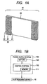
FIG. 1A illustrates an example of a dust removing device according to the present invention. -
FIG. 1B is a circuit block diagram of the dust removing device according to the present invention. -
FIG. 2 illustrates another example of the dust removing device according to the present invention. -
FIGS. 3A, 3B and 3C illustrate an example of a piezoelectric device according to the present invention. -
FIGS. 4A and 4B are schematic views illustrating a vibration principle of the piezoelectric device according to the present invention. -
FIGS. 5A and 5B illustrate a vibration principle of a conventional piezoelectric device. -
FIGS. 6A and 6B are schematic views illustrating a vibration principle of the dust removing device according to the present invention. -
FIGS. 7A and 7B are schematic views illustrating a vibration principle of a conventional dust removing device. -
FIGS. 8A and 8B are schematic views illustrating the vibration principle of the dust removing device according to the present invention. -
FIG. 9A is a schematic view illustrating a waveform to be formed on a vibrating plate of the dust removing device according to the present invention. -
FIG. 9B is a schematic view illustrating a waveform to be formed on a vibrating plate of the conventional dust removing device. -
FIGS. 10A and 10B are schematic views each illustrating an embodiment of the dust removing device according to the present invention. -
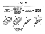
FIG. 11 is a schematic view illustrating a process of manufacturing the piezoelectric device according to the present invention. -
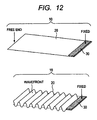
FIG. 12 is view illustrating a calculation model for a vibration of a dust removing device according to Example 1. -
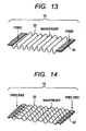
FIG. 13 is view illustrating a calculation model for a vibration of a dust removing device according to Example 2. -
FIG. 14 is view illustrating a calculation model for a vibration of the dust removing device according to Comparative Example 2. -
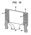
FIG. 15 is a schematic view of the dust removing device according to the present invention, to which flexible wiring cables are connected. - Preferred embodiments of the present invention will now be described in detail in accordance with the accompanying drawings.
- In the following, an embodiment for carrying out the present invention is described.
- A dust removing device according to the present invention is a dust removing device to be installed on a base, which includes a piezoelectric device in the form of a plate at least including a piezoelectric material in the form of a plate and a pair of electrodes being disposed to be opposed to each other on plate surfaces of the piezoelectric material, and a vibrating plate. The dust removing device has features in that the piezoelectric device has a first electrode plane fixedly bonded to a plate surface of the vibrating plate, the piezoelectric material is polarized in parallel with the first electrode plane, and the dust removing device is fixed to the base through a second electrode plane of the piezoelectric device.
- A dust removing method according to the present invention is a method of removing dust adhering to a vibrating plate installed on a base via a piezoelectric device in a form of a plate, which at least includes a piezoelectric material in a form of a plate and a pair of electrodes disposed to be opposed to each other on plate surfaces of the piezoelectric material. The method is featured by including: fixedly bonding a first electrode plane of the piezoelectric device to a plate surface of the vibrating plate, fixing a second electrode plane of the piezoelectric device to the base, and driving and vibrating the piezoelectric device after polarizing the piezoelectric material in parallel with the first electrode plane; and generating a vibration in the vibrating plate by the vibration of the piezoelectric device to thereby remove dust adhering to a surface of the vibrating plate.
-
FIGS. 1A, 1B , and2 are schematic views each illustrating an example of the dust removing device of the present invention. For illustration, in the schematic views, components such as a power supply line from a power supply system are omitted from the drawings. - Referring to
FIG. 1A , thedust removing device 10 includes apiezoelectric device 30 in the form of a plate and a vibratingplate 20. - With reference to a block diagram of
FIG. 1B , a configuration of the dust removing device according to the present invention is described. Apower supply system 100 includes acontrol portion 110 including amemory 111, and abattery 120. Thedust removing device 10 is connected to thecontrol portion 110 in thepower supply system 100 via, for example, a flexible cable. Thecontrol portion 110 is configured to control thedust removing device 10 based on an alternating voltage generated from power supplied by thebattery 120. - The
piezoelectric device 30 is formed of, as illustrated inFIGS. 3A to 3C , apiezoelectric material 31, afirst electrode 32, and asecond electrode 33. Thefirst electrode 32 and thesecond electrode 33 are each disposed to be opposed to plate surfaces of thepiezoelectric material 31. One surface of thepiezoelectric material 31 is defined as afirst electrode plane 36, on which thefirst electrode 32 ofFIG. 3C on the right in front of thepiezoelectric device 30 is formed. Another surface of thepiezoelectric material 31 is defined as asecond electrode plane 37, on which thesecond electrode 33 ofFIG. 3A on the left in front of thepiezoelectric device 30 is formed. Here, the electrode plane in this embodiment refers to a surface of the piezoelectric device on which an electrode is formed, and, as illustrated inFIGS. 3A and 3B , for example, thefirst electrode 32 may be extended to come around to thesecond electrode plane 37. - As illustrated in
FIG. 2 , thepiezoelectric device 30 is fixedly bonded to a plate surface of the vibratingplate 20 through thefirst electrode plane 36 of thepiezoelectric device 30. When thepiezoelectric device 30 is driven, a stress is generated between thepiezoelectric device 30 and the vibratingplate 20, to thereby generate a flexural vibration in the vibratingplate 20. Thedust removing device 10 according to the present invention removes dust adhering to a surface of the vibratingplate 20 through application of the flexural vibration thus generated in the vibratingplate 20. The flexural vibration refers to an elastic vibration for causing a displacement of the vibratingplate 20 in an optical axis direction, that is, in a thickness direction of the vibratingplate 20. - In the following, the difference between the
piezoelectric device 30 according to the present invention and apiezoelectric device 40 of a conventional example is described in detail. -
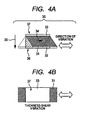
FIGS. 4A and 4B are schematic views illustrating a vibration principle of thepiezoelectric device 30 according to the present invention.FIG. 4A is a schematic view illustrating in section thepiezoelectric device 30 in the form of a plate, andFIG. 4B is a schematic view illustrating from above thesecond electrode plane 37 of thepiezoelectric device 30 in the form of a plate. As illustrated inFIGS. 4A and 4B , in thepiezoelectric device 30 of the present invention, thepiezoelectric material 31 is polarized in advance in parallel with thefirst electrode plane 36 so that thefirst electrode 32 and thesecond electrode 33 may be applied with a high-frequency voltage by, for example, a drive power supply of the digital camera main body. - In the
piezoelectric device 30 according to the present invention, an alternating electric field generated in a direction of thearrow 35 ofFIG. 4A causes a shearing strain to occur in thepiezoelectric material 31. The shearing strain causes an elastic vibration (hereinafter, defined as thickness-shear vibration) for displacing thefirst electrode plane 36 and thesecond electrode plane 37 from each other in the length direction of thepiezoelectric device 30. As illustrated inFIGS. 4A and 4B , in the thickness-shear vibration, thepiezoelectric material 31 is polarized in parallel with the first electrode plane 36 (in a direction of thearrow 34 ofFIG. 4A ), and the electric field is applied in the thickness direction of thepiezoelectric device 30. At this time, a direction of vibration of thepiezoelectric device 30 permissible in the length direction is only in a direction parallel to apolarization axis direction 34 of thepiezoelectric material 31. A magnitude of the thickness-shear vibration in thepiezoelectric device 30 is closely related to a magnitude of the piezoelectric displacement resulting from the piezoelectric thickness-shear effect of the piezoelectric ceramics. - Meanwhile,
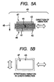
FIGS. 5A and 5B are schematic views illustrating a vibration principle of the conventionalpiezoelectric device 40.FIG. 5A is a schematic view illustrating in section thepiezoelectric device 40 in the form of a plate, andFIG. 5B is a schematic view illustrating from above asecond electrode plane 47 of thepiezoelectric device 40 in the form of a plate. As illustrated inFIGS. 5A and 5B , in thepiezoelectric device 40 of the conventional example, apiezoelectric material 41 is polarized in advance in parallel with afirst electrode plane 46 so that afirst electrode 42 and asecond electrode 43 may be applied with a high-frequency voltage by, for example, a drive power supply of the digital camera main body. - In the
piezoelectric device 40 of the conventional example, an alternating electric field generated in a direction (electric field direction) of thearrow 45 ofFIG. 5A causes a stretching strain to occur in thepiezoelectric material 41. The stretching strain causes the length vibration of thepiezoelectric device 40. As illustrated inFIGS. 5A and 5B , in the length vibration, thepiezoelectric material 41 is polarized perpendicularly to the first electrode plane 46 (in a direction of the arrow 44), and the electric field is applied in the thickness direction of thepiezoelectric device 40. At this time, a direction of vibration of thepiezoelectric device 40 permissible in the length direction is any direction perpendicular to apolarization axis direction 44 of thepiezoelectric material 41, without depending on the shape, such as a rectangular shape or a cylindrical shape, of thepiezoelectric device 40. A magnitude of the length vibration in thepiezoelectric device 40 is closely related to a magnitude of the piezoelectric displacement resulting from the piezoelectric transverse effect of the piezoelectric ceramics. - By the way, in the
piezoelectric device 30 according to the present invention, even when one of thefirst electrode plane 36 and thesecond electrode plane 37 of thepiezoelectric device 30 is completely fixed, thepiezoelectric device 30 itself still can generate the thickness-shear vibration. For example, as illustrated inFIGS. 4A and 4B , when thepiezoelectric device 30 of the present invention is driven under a state in which thesecond electrode plane 37 of thepiezoelectric device 30 is fixed to the base, thesecond electrode plane 37 of thepiezoelectric device 30 does not vibrate due to the fixation, whereas thepiezoelectric device 30 of the present invention is driven in the thickness-shear vibration, and hence thefirst electrode plane 36 of thepiezoelectric device 30 can vibrate in the length direction of thepiezoelectric device 30. Here, when thesecond electrode plane 37 of thepiezoelectric device 30 is fixed to the base, the movement of thesecond electrode plane 37 of thepiezoelectric device 30 is completely locked at least in the length direction with respect to the base. Here, the base according to the present invention collectively means at least one member capable of completely locking the movement of thesecond electrode plane 37 of thepiezoelectric device 30 at least in the length direction with respect to the base, and refers to a member having sufficient mass and rigidity capable of generating the flexural vibration in the vibratingplate 20 through thepiezoelectric device 30. - On the other hand, in the conventional
piezoelectric device 40, when one of thefirst electrode plane 46 and thesecond electrode plane 47 of thepiezoelectric device 40 is fixed, thepiezoelectric device 40 itself is hindered to generate the length vibration. For example, as illustrated inFIGS. 5A and 5B , when the conventionalpiezoelectric device 40 is driven under a state in which thesecond electrode plane 47 of thepiezoelectric device 40 is fixed to the base, thepiezoelectric device 40 itself fails to vibrate almost completely in all directions under the constraint of the fixedsecond electrode plane 47 because thepiezoelectric device 40 is driven in the length vibration. The hindrance to thepiezoelectric device 40 becomes more noticeable as thepiezoelectric device 40 is reduced in thickness, and thepiezoelectric device 40 in a conventional shape fails to vibrate almost completely. - Unlike the
piezoelectric device 40 according to the conventional technology, thepiezoelectric device 30 of the present invention has a feature that thepiezoelectric device 30 is capable of generating a desired piezoelectric vibration even when thesecond electrode plane 37 of thepiezoelectric device 30 is fixed to the base. - A magnitude of the thickness-shear vibration of the
piezoelectric device 30 of the present invention is closely related to a magnitude of the piezoelectric displacement resulting from the piezoelectric thickness-shear effect of the piezoelectric ceramics. On the other hand, in the conventionalpiezoelectric device 40, a magnitude of the length vibration in thepiezoelectric device 40 is closely related to a magnitude of the piezoelectric displacement resulting from the piezoelectric transverse effect of the piezoelectric ceramics. - As described above, the magnitude of the piezoelectric displacement resulting from the piezoelectric thickness-shear effect of the piezoelectric ceramics is equal to or more than twice as large as the magnitude of the piezoelectric displacement resulting from the piezoelectric transverse effect. In other words, the
piezoelectric device 30 of the present invention has a larger displacement function, as compared to the conventionalpiezoelectric device 40, even when the same piezoelectric material is used. Conversely, it can be said that thepiezoelectric device 30 of the present invention has a displacement function equal to that of the conventionalpiezoelectric device 40, even when a piezoelectric material with a smaller piezoelectric constant is used. - Next, the difference between the
dust removing device 10 of the present invention and the conventional dust removing device is described in detail. -
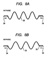
FIGS. 6A and 6B are schematic views illustrating the vibration principle of thedust removing device 10 according to the present invention.FIG. 6A illustrates a state in which a pair of thepiezoelectric devices 30 on the right and left are applied with alternating voltages in the same phase to generate the flexural vibration in the vibratingplate 20. The pair of thepiezoelectric devices 30 on the right and left face each other with thepiezoelectric materials 31 being opposed to each other in polarization, and thedust removing device 10 is driven in a seventh order vibration mode.FIG. 6B illustrates a state in which a pair of thepiezoelectric devices 30 on the right and left are applied with alternating voltages in a reversed phase, which are opposite in phase by 180 degrees, to generate the flexural vibration in the vibratingplate 20. The pair of thepiezoelectric devices 30 on the right and left face each other with thepiezoelectric materials 31 being opposed to each other in polarization, and thedust removing device 10 is driven in a sixth order vibration mode. In thedust removing device 10 of the present invention, at least two vibration modes are selectively used effectively as described above, to thereby remove dust adhering to the surface of the vibratingplate 20 with efficiency. - On the other hand,
FIGS. 7A and 7B are schematic views illustrating a vibration principle of a conventionaldust removing device 15.FIG. 7A illustrates a state in which a pair of thepiezoelectric devices 40 on the right and left are applied with alternating voltages in the same phase to generate the flexural vibration in a vibratingplate 25. In the pair of thepiezoelectric devices 40 on the right and left, thepiezoelectric materials 41 are polarized in the same direction in the thickness direction of thepiezoelectric devices 40, and thedust removing device 15 is driven in a seventh order vibration mode.FIG. 7B illustrates a state in which the pair of thepiezoelectric devices 40 on the right and left are applied with alternating voltages in a reversed phase, which are opposite in phase by 180 degrees, to generate the flexural vibration in the vibratingplate 25. In the pair of thepiezoelectric devices 40 on the right and left, thepiezoelectric materials 41 are polarized in the same direction in the thickness direction of thepiezoelectric devices 40, and thedust removing device 15 is driven in a sixth order vibration mode. In the conventionaldust removing device 15, similarly to thedust removing device 10 of the present invention, at least two vibration modes are selectively used effectively, to thereby remove dust adhering to the surface of the vibrating plate with efficiency. - In the
dust removing device 10 of the present invention, thepiezoelectric device 30 is fixed to the base through thesecond electrode plane 37, and the vibratingplate 20 does not generate the flexural vibration in a part on which thepiezoelectric device 30 is disposed. On the other hand, in the conventionaldust removing device 15, the vibratingplate 25 generates the flexural vibration even in a part on which thepiezoelectric device 40 is disposed. Accordingly, one of thepiezoelectric devices 40 and at least in part of both of the plate surfaces of the vibratingplate 25 need to be held by a certain holding member so as to be fixed to the base by means of the holding member. However, the vibratingplate 25 generates the flexural vibration, and hence, if thedust removing device 15 is held by a pressing member or a holding member, the pressing member or the holding member cannot hold the vibratingplate 25 without affecting the vibration thereof, no matter where the vibratingplate 25 is held. Therefore, according to a configuration of the conventionaldust removing device 15, the dust removal performance is degraded when thedust removing device 15 is held to be fixed to the base. On the other hand, in thedust removing device 10 of the present invention, there is no need to hold the vibratingplate 20 to be fixed to the base, and the vibratingplate 20 can be fixed to the base without degrading the dust removal performance. - In the example illustrated in
FIGS. 6A and 6B , the pair of thepiezoelectric devices 30 on the right and left face each other with polarizations thereof being opposed to each other. However, the polarizations need not be opposed to each other as long as the polarization axes are parallel to each other, and the pair of thepiezoelectric devices 30 may face each other as illustrated inFIG. 8B . In this case, when the pair of thepiezoelectric devices 30 are applied with alternating voltages in the same phase, the vibration mode in the reversed phase as illustrated inFIG. 6B may be obtained. - In the above, the
dust removing device 10 of the present invention is described, which includes, as illustrated inFIGS. 1A and2 , the pair of the plate-likepiezoelectric devices 30 each in a rectangular solid shape and the vibratingplate 20 in a rectangular solid shape. As described above, thedust removing device 10, according to a most preferred configuration of thedust removing device 10 of the present invention, includes at least a pair of the plate-likepiezoelectric devices 30 each in a rectangular solid shape, which are disposed on end portions of the vibratingplate 20 in a rectangular solid shape to be opposed to each other across a central region of the vibratingplate 20, in which thepolarization axis direction 34 is parallel to a direction in which the pair of thepiezoelectric devices 30 are opposed to each other. - However, the
dust removing device 10 of the present invention is not necessarily limited to the above-mentioned configuration. Thedust removing device 10 according to the present invention may be thedust removing device 10 to be installed on a base, which includes thepiezoelectric device 30 in the form of a plate at least including at least thepiezoelectric material 31 in the form of a plate and a pair of opposed electrodes each being disposed on a plate surface of thepiezoelectric material 31 and the vibratingplate 20. In thedust removing device 10, thefirst electrode plane 36 of thepiezoelectric device 30 may be fixedly bonded to a plate surface of the vibratingplate 20, thepiezoelectric material 31 may be polarized in a direction parallel to thefirst electrode plane 36, and thepiezoelectric device 30 may be driven by the thickness-shear vibration with thesecond electrode plane 37 being a reference plane. Here, the reference plane refers to a plane serving as a reference of the vibration of thepiezoelectric device 30. When thepiezoelectric device 30 vibrates with reference to thesecond electrode plane 37 as a reference plane, the vibration of thefirst electrode plane 36 of thepiezoelectric device 30 in the length direction reaches a maximum. Accordingly, in the above-mentioned configuration, the flexural vibration of the vibratingplate 20 fixedly bonded to thepiezoelectric device 30 through thefirst electrode plane 36 reaches a maximum. - For example, when the
dust removing device 10 of the present invention is fixed to the base through the reference surface, a desired piezoelectric vibration may be generated in thedust removing device 10. Accordingly, in thedust removing device 10 of the present invention, the vibratingplate 20 does not need to be held to be fixed, and hence can be fixed to the base without degrading the dust removal performance. At the same time, thedust removing device 10 of the present invention is fixed to the base through the reference plane, which offers a feature that the flexural vibration of the vibratingplate 20 reaches a maximum. In other words, thedust removing device 10 of the present invention is most preferred to be fixed to the base through the reference plane. Further, in thedust removing device 10 of the present invention using the same piezoelectric material as that of the conventionaldust removing device 15, thepiezoelectric device 30 has a larger displacement capability. In other words, the present invention may provide thedust removing device 10, which is capable of utilizing the displacement capability inherent in thepiezoelectric device 30 and achieving high dust removal performance, and easy to fix. - The
piezoelectric material 31 forming thedust removing device 10 of the present invention is polarized in a direction parallel to thefirst electrode plane 36. However, the polarization direction may not necessarily be in complete parallel with thefirst electrode plane 36. For example, even when thepolarization axis direction 34 is at an angle of 5 degrees from a complete parallel with respect to thefirst electrode plane 36, the effect of the displacement capability of thepiezoelectric device 30 is reduced by 0.5%, which is 1.5% with the angle of 10 degrees. Accordingly, the polarization axis may be allowed to be at an angle of 10 degrees at maximum. Further, in thedust removing device 10 of the present invention, thepiezoelectric device 30 has thefirst electrode plane 36 fixedly bonded to the plate surface of the vibratingplate 20. Here, when thepiezoelectric device 30 is fixedly bonded to the vibratingplate 20 according to the present invention, thepiezoelectric device 30 is restrained in a manner that a stress is generated at least between thepiezoelectric device 30 and the vibratingplate 20 so that the flexural vibration is generated in the vibratingplate 20. - In the
dust removing device 10 of the present invention, thepiezoelectric device 30 and the vibratingplate 20 may contact each other across an area smaller than 1/2 of an area of the vibratingplate 20. In a case where thepiezoelectric device 30 and the vibratingplate 20 contact with each other across an area larger than 1/2 of an area of the vibratingplate 20, the vibratingplate 20 does not vibrate in an area larger than the half of the entire area of the vibratingplate 20, which leads to degradation of dust removal performance. - Further, in the
dust removing device 10 of the present invention, thepiezoelectric device 30 may be preferred to be in a rectangular solid shape, with being polarized in a direction parallel to any one of the sides of the rectangular solid shape. The reason is as follows. - In the dust removing device of the present invention and in the conventional dust removing device, the flexural vibration generated in the vibrating plate forms a wavefront on the vibrating plate. The wavefront formed on the vibrating plate is parallel to the length direction of the piezoelectric device in a rectangular solid shape. In other words, the wavefront has a cross section in the length direction illustrated in each of
FIGS. 6A to 8B . Here,FIGS. 6A to 8B each illustrate a certain section in the length direction of the wavefront. However, the dust removing device of the present invention or the conventional dust removing device is preferred to be capable of forming the wavefront illustrated in each ofFIGS. 6A to 8B in the same shape, in a frontward direction and in a backward direction on the paper plane. -
FIG. 9A illustrates a wavefront formed on the vibratingplate 20 of the dust removing device of the present invention. InFIG. 9A , thepolarization axis direction 34 is parallel to a direction of a short side (hereinafter, referred to as lateral direction) which is orthogonal to the length direction of thepiezoelectric device 30 in a rectangular solid shape, and the wavefront on the vibratingplate 20 is parallel to a direction of a long side (hereinafter, referred to as longitudinal direction) which is parallel to the length direction of thepiezoelectric device 30 in a rectangular solid shape. Here, the same wavefront on the vibratingplate 20 may be formed with substantially equal amplitude in the longitudinal direction of thepiezoelectric device 30 in a rectangular solid shape. The reason is that thepiezoelectric device 30 of the present invention generates a thickness-shear vibration. As illustrated inFIG. 9A , thepiezoelectric device 30 of the present invention vibrates only in a direction parallel to the polarization direction, and does not vibrate in any other length direction which is not parallel to the polarization direction. Accordingly, in thedust removing device 10 of the present invention, the wavefronts as illustrated inFIGS. 6A to 8B may be formed in a similar shape in a frontward direction and in a backward direction on the paper plane, that is, in the longitudinal direction of thepiezoelectric device 30 in a rectangular solid shape, to thereby uniformly deliver dust removal performance across the entire area of the vibratingplate 20. - On the other hand,
FIG. 9B illustrates a wavefront formed on the vibratingplate 25 of the conventional dust removing device. InFIG. 9B , thepolarization axis direction 44 is parallel to the thickness direction of thepiezoelectric device 40 in a rectangular solid shape, and the wavefront on the vibratingplate 25 is parallel to a longitudinal direction of thepiezoelectric device 40 in a rectangular solid shape. However, the same wavefront on the vibratingplate 25 may be difficult to be formed with substantially equal amplitude in the longitudinal direction of thepiezoelectric device 40 in a rectangular solid shape. The reason is that the conventionalpiezoelectric device 40 generates a length vibration. As illustrated inFIG. 9B , the conventionalpiezoelectric device 40 vibrates omnidirectionally in the length direction of thepiezoelectric device 40. In particular, in the case where thepiezoelectric device 40 is in a rectangular solid shape, the wavefront on the vibratingplate 25 is to be formed by a combined vibration which is greatly affected by the vibrations in the lateral direction and in the longitudinal direction of thepiezoelectric device 40 in a rectangular solid shape. Accordingly, in the conventionaldust removing device 15, the wavefronts illustrated inFIGS. 6A to 8B may not be formed in a similar shape in the longitudinal direction of thepiezoelectric device 40 in a rectangular solid shape, and hence the dust removal performance greatly varies depending on the area on the vibratingplate 25. - Due to the difference as described above, the
dust removing device 10 of the present invention, in which thepiezoelectric device 30 is in a rectangular solid shape and thepolarization axis direction 34 is in parallel with any one of the sides of the rectangular solid shape, offers dust removal performance superior to that of the conventionaldust removing device 15. According to the present invention, the shape of the vibratingplate 20 of thedust removing device 10 is not specifically limited, but the wavefront of the vibratingplate 20 formed on the vibratingplate 20 is also influenced by the shape of the vibratingplate 20. Further, the amplitude of the flexural vibration generated in the vibratingplate 20 is influenced by the material and the thickness of the vibratingplate 20. Accordingly, the vibratingplate 20 may be preferred to be in plate-like rectangular solid shape. In particular, the vibratingplate 20 is preferred to have a minimum thickness and hardness capable of fulfilling the function of the vibratingplate 20 while ensuring adequate strength therefor. - In the
dust removing device 10 of the present invention, thepiezoelectric device 30 is preferred to be disposed on an end portion on the plate surface of the vibratingplate 20. When thepiezoelectric device 30 is disposed on the end portion on the plate surface of the vibratingplate 20, the vibration of thepiezoelectric device 30 may be efficiently transmitted across the entire surface of the vibratingplate 20, to thereby efficiently deliver dust removal performance. Here, thepiezoelectric device 30 does not necessarily need to be in complete contact with the end portion on the plate surface of the vibratingplate 20. For example, thedust removing device 10 may be disposed in a periphery close to the end portion of the vibratingplate 20, as long as thedust removing device 10 is disposed in a peripheral portion in which there is no practical need to remove dust. - Further, when multiple
piezoelectric devices 30 are provided, the multiplepiezoelectric devices 30 may be effectively controlled, to thereby form a desired wavefront across the entire surface of the vibratingplate 20. In particular, in thedust removing device 10 of the present invention, at least a pair of thepiezoelectric devices 30 may be preferred to be disposed across a central region of the vibratingplate 20, and thepolarization axis direction 34 may be preferred to be parallel to a direction in which the pair of thepiezoelectric devices 30 are opposed to each other. - The
dust removing device 10 of the present invention configured as described above offers excellent dust removal performance. The configuration is illustrated inFIGS. 10A and 10B . Thepiezoelectric devices 30 do not need to be opposed to each other as long as the polarization axes 34 thereof are parallel to each other. Further, as illustrated inFIG. 10B , the polarization direction of each of the multiple portions of thepiezoelectric devices 30 is not specifically limited, as long as each pair of the multiple portions of thepiezoelectric devices 30 have thepolarization axis directions 34 parallel to the direction in which the pair of the multiple portions of thepiezoelectric devices 30 are opposed to each other. - In the
dust removing device 10 of the present invention, thepiezoelectric device 30 may be preferred to be formed of a material having a lead (Pb) content of 1,000 ppm or less, and may be preferred to be formed of piezoelectric ceramics containing, for example, barium titanate as a major component. When the Pb content is 1,000 ppm or less, the lead component in the piezoelectric material is less likely to adversely affect the environment even when the dust removing device is discarded to receive acid rain and be exposed to a harsh environment. - The lead-free piezoelectric ceramics as described above are inferior in various properties to piezoelectric ceramics of lead zirconate titanate (PZT) under the present circumstances. However, for example, when the lead-free piezoelectric ceramics contain barium titanate as a major component, the magnitude of the piezoelectric displacement due to the piezoelectric thickness-shear effect is larger than the magnitude of the piezoelectric displacement due to the piezoelectric transverse effect, and even larger than the magnitude of the piezoelectric displacement due to the piezoelectric transverse effect of PZT, which is mainly used in the conventional
dust removing device 15. In other words, in thedust removing device 10 according to the present invention, even when the piezoelectric ceramics as described above are used for thepiezoelectric material 31, a dust removal effect equal to or larger than that of the conventionaldust removing device 15 may be offered. Here, for example, in a case where the lead-free piezoelectric ceramics are piezoelectric ceramics containing barium titanate as a major component, the piezoelectric ceramics may include, as an accessory component, an element forming Pb or PZT, and in this case, the Pb content is preferred to be 1,000 ppm or less. - Further, the
piezoelectric material 31 is preferred to have a large mechanical quality factor Qm. For example, in the case where the lead-free piezoelectric ceramics contain barium titanate as a major component, Qm may be increased to be equal to that of PZT through the addition of, for example, manganese (Mn), and accordingly thedust removing device 10 of the present invention may further be improved in dust removal performance. - The
dust removing device 10 of the present invention has a feature that the vibratingplate 20 is formed of an optical material. The optical material according to the present invention refers to a material having an optical function with respect to incident light. Examples of the optical function include transmittance, refraction, interference, reflection, and scattering. The vibratingplate 20 may have, in addition to the function as the vibrating plate, an optical function to serve as, for example, an infrared cut filter or an optical low-pass filter. Here, the infrared cut filter is an optical member for blocking the transmission of near-infrared light (IR) while allowing visible light to pass therethrough, and is formed of, for example, glass. Further, the optical low-pass filter is an optical member for separating transmitted light into an ordinary beam and an extraordinary beam in order to eliminate high spatial frequency component of the light, and includes, for example, a multilayer of birefringent plates and phase plates which are made of crystal. - The dust removing device of the present invention is mounted on the base including, for example, an image pickup device such as a digital camera, and an image reading device such as a scanner.
- Further, the vibrating
plate 20 may be coated with a conductive material or the like in order to prevent dust from electrically adhering thereto. Further, the vibratingplate 20 may include multiple members separately having the above-mentioned different functions. In this case, for the vibratingplate 20, a member having a largest possible mechanical quality factor may be preferred to be selected as long as the member is capable of attaining the necessary functions as the vibratingplate 20. - Next, a method of manufacturing the
dust removing device 10 of the present invention is described with reference to thedust removing device 10 illustrated inFIGS. 1A and2 , in which at least a pair of thepiezoelectric devices 30 each in a plate-like rectangular solid shape are disposed on both end portions of the vibratingplate 20 in a rectangular solid shape to be opposed to each other across a central region of the vibratingplate 20, and thepolarization axis direction 34 is parallel to a direction in which the pair of thepiezoelectric devices 30 are opposed to each other. - According to the method of manufacturing the
piezoelectric device 30 of the present invention, first, a piezoelectric ceramics powder which is adjusted to have a desired composition is added with a sintering agent such as a dispersant, and then is pressed into a shape with a pressure necessary for forming a high-density sintered body, to thereby manufacture a piezoelectric ceramics compact. Here, in a case where the necessary pressure cannot be obtained merely by the press forming, a desired pressure may be applied through, for example, cold isostatic press (CIP). Alternatively, without performing press forming, a compact ingot of piezoelectric ceramics may be formed through CIP or the like from the beginning. Next, the piezoelectric ceramics compact is baked, to thereby manufacture a piezoelectric ceramics sintered body. Any baking method appropriate for desired piezoelectric ceramics may be selected. Note that, if necessary, the piezoelectric ceramics compact may be processed into a desired shape before baking. - Next, the piezoelectric ceramics sintered body thus manufactured is subjected to grinding processing, to thereby manufacture piezoelectric ceramics in a rectangular solid shape having a desired dimension. Here, the piezoelectric ceramics after being baked serve as the
piezoelectric material 31 of the present invention. However, the piezoelectric ceramics do not necessarily need to be processed to have a dimension of thepiezoelectric device 30, or do not necessarily be in a rectangular solid shape. - The
piezoelectric material 31 of the present invention is subjected to polarization treatment, generally at a temperature lower than the Curie temperature or the depolarization temperature of thepiezoelectric material 31, for 5 minutes to 10 hours, in the air or in an incombustible oil such as a silicon oil, through application of an electric field of 0.5 to 5.0 kV/mm. In thepiezoelectric material 31 of the present invention, thepolarization axis direction 34 is eventually formed in the length direction of the plate-likepiezoelectric material 31. Accordingly, thepiezoelectric material 31 in a rectangular solid shape may be preferred to be equal to or smaller than 30 mm at a maximum in length in thepolarization axis direction 34. In a case where thepiezoelectric material 31 has a length larger than 30 mm, a power supply capable of applying a significantly large voltage becomes necessary when subjecting thepiezoelectric material 31 to the polarization treatment. - The
piezoelectric device 30 of the present invention is generally 0.1 mm to 10 mm in thickness. Accordingly, formation of an electrode, which is to be used for subjecting thepiezoelectric material 31 to the polarization treatment, on a surface of the piezoelectric material in a rectangular solid shape, the surface being in parallel with the thickness direction of thepiezoelectric material 31, and application of a desired voltage necessary for the polarization treatment are difficult. In view of this, as illustrated in, for example, a schematic view ofFIG. 11 illustrating a process of manufacturing thepiezoelectric device 30, thepiezoelectric material 31 in a rectangular solid shape may be formed thick when performing the polarization treatment, and the electrode for the polarization treatment may be formed on a wide surface. After that, the rectangular solid shape after being subjected to the polarization treatment may be subjected to grinding processing so that the rectangular solid shape may be ground into a desired dimension of thepiezoelectric device 30, and then thefirst electrode 32 and thesecond electrode 33 are formed as illustrated inFIG. 3 , to thereby manufacture thepiezoelectric device 30 of the present invention. At this time, in order to prevent thefirst electrode 32 and thesecond electrode 33 from being short-circuited, the electrode for the polarization treatment may be preferred to be removed through grinding processing after the polarization treatment. The electrode for the polarization treatment, thefirst electrode 32, and thesecond electrode 33 may be formed through, for example, printing of a silver paste, Au sputtering, or Au plating. However, after the polarization treatment, the device needs to be manufactured at a temperature lower than the Curie temperature or the depolarization temperature of thepiezoelectric material 31, and hence the device may be preferred to be manufactured by a method which can be performed without increasing the formation temperature. Further,FIG. 11 illustrates an example in which onepiezoelectric device 30 is formed from onepiezoelectric material 31 in a rectangular solid shape which has been subjected to polarization treatment. However, the number of thepiezoelectric devices 30 is not necessarily limited to one, and multiplepiezoelectric devices 30 may be formed from onepiezoelectric material 31 in a rectangular solid shape. - As described above, the
piezoelectric material 31 of the present invention may be preferred to be subjected to polarization treatment in advance in the process of manufacturing thepiezoelectric device 30, which is, however, not an absolute necessity. For example, thefirst electrode 32 and thesecond electrode 33 may be formed in part on an end portion diagonal to thefirst electrode plane 36 and thesecond electrode plane 37 of thepiezoelectric device 30 which has been ground to a desired dimension of thepiezoelectric device 30. After polarization treatment is performed by using those electrodes, the rest of thefirst electrode 32 and thesecond electrode 33 may be formed, to thereby manufacture thepiezoelectric device 30. In this case, when the ratio of the thickness of thepiezoelectric device 30 with respect to a distance between thefirst electrode 32 and thesecond electrode 33 each being disposed on the diagonal end portion is equal to or smaller than 17 to 100, thepolarization axis direction 34 of thepiezoelectric material 31 may be formed at an angle equal to or smaller than 10 degrees from a complete parallel with respect to thefirst electrode plane 36. - Next, as illustrated in
FIGS. 1A and2 , the twopiezoelectric devices 30 are fixedly bonded to the vibratingplate 20 formed into a desired dimension. At this time, thepiezoelectric devices 30 each may be disposed so as to have thefirst electrode plane 36 of thepiezoelectric device 30 disposed on an end portion on a plate surface of the vibratingplate 20. Thepiezoelectric devices 30 and the vibrating plate may be fixedly bonded to each other through, for example, an epoxy resin adhesive. An adhesive that may not degrade adhesiveness in the operating temperature range of thedust removing device 10 or the mechanical quality factor Qm of thedust removing device 10 may be preferred to be selected. Further, thepiezoelectric device 30 has already been subjected to polarization treatment, and hence the bonding temperature may be preferred to be smaller than the Curie temperature or the depolarization temperature of thepiezoelectric material 31. - In the above, the method of manufacturing the
dust removing device 10 of the present invention is described in detail with reference to thedust removing device 10 illustrated inFIGS. 1A and2 , in which at least a pair of thepiezoelectric devices 30 each in a plate-like rectangular solid shape are disposed on both end portions of the vibratingplate 20 in a rectangular solid shape to be opposed to each other across a central region of the vibratingplate 20, and thepolarization axis direction 34 is parallel to a direction in which the pair of thepiezoelectric devices 30 are opposed to each other. Thedust removing device 10 of the present invention may not necessarily have the above-mentioned configuration. In such a case, an optimal manufacturing method may be selected as appropriate. - Example 1
- In the following, the dust removing device of the present invention is specifically described with reference to Examples. However, the present invention is not limited by the following Examples.
- First, a method of manufacturing the piezoelectric device of the present invention is described. Barium titanate particles with an average particle diameter of 100 nm (manufactured by Sakai Chemical Industry Co., Ltd., BT-03 as a trade name) were coated with manganese acetate (II) by using a spray dryer. According to inductively coupled plasma (ICP) mass spectrometry, the powder mix had a manganese content of 0.12% by mass.
- Next, the powder mix was added with a polyvinyl alcohol aqueous solution at a concentration of 5% by mass, as a dispersant. The additive amount was determined so that polyvinyl alcohol in the polyvinyl alcohol aqueous solution was 3% by mass with respect to the powder mix. The mixture was mixed in a mortar, to thereby manufacture a granulated powder mix. The granulated powder mix was charged by 5.0 g into a mold in a size of 45.0×7.0 mm, and subjected uniaxial press forming under a pressure of 200 MPa. Next, the compact was baked in an electric furnace at 1,380°C in an air atmosphere for two hours. The rate of temperature increase was 10°C per minute, and the temperature was held at 600°C for three hours during the increase, to thereby manufacture the piezoelectric material of the present invention. The piezoelectric material thus obtained had dimensions of 36.4x5.75x4 mm.
- Next, polarization treatment electrodes were formed by using a silver paste on two surfaces each being in a size of 5.75x4 mm of the piezoelectric material, and the piezoelectric material was subjected to polarization treatment in a silicon oil by using a direct power supply. The temperature of the oil was 100°C, the applied electric field was 1 kV/mm, and the voltage was applied for 30 minutes at 100°C. Next, the piezoelectric material after the polarization treatment was subjected to grinding processing to be ground to be in a size of 36.4x5.75xO.25 mm, and the first electrode and the second electrode were pattern-formed in thicknesses of 30 nm and 380 nm, respectively, on two surfaces each being in a size of 36.4x5.75 mm of the piezoelectric material through DC magnetron sputtering in order of Ti to Au. Next, the piezoelectric material in a size of 36.4×5.75×0.25 mm was cut into a size of 33.3x4.0x0.25 mm, and then a diffraction electrode was pattern-formed through the above-mentioned DC magnetron sputtering in order of Ti to Au, so that the first electrode on the first electrode plane and the first electrode on the second electrode plane were short-circuited via one of the surfaces in a size of 4.0x0.25 mm of the piezoelectric material. At this time, it was confirmed that the first electrode and the second electrode were not short-circuited, to thereby manufacture the piezoelectric device of the present invention as illustrated in
FIG. 3 . Here, the polarization axis direction of the piezoelectric device was in a direction parallel to the side of 4 mm of the piezoelectric material in a rectangular solid shape. - Further, the piezoelectric device of the present invention was bonded through an epoxy resin adhesive along one side of 33.7 mm of the surface of a glass plate in a size of 50.8x33.7x0.3 mm serving as an infrared cut filter, to thereby manufacture the dust removing device according to Example 1 of the present invention.
- In order to confirm the effect of Example 1, frequency response calculation based on a finite element method was performed. This calculation was performed by using a finite element method packaged software ANSYS (manufactured by ANSYS Inc.). The dust removing device used as a model included the vibrating plate in a size of 50.8×33.7×0.3 mm, and the piezoelectric device in a size of 33.3×4.0×0.25 mm. The input values were an elastic coefficient, a density, and a Poisson ratio of the vibrating plate, and a dielectric constant, a piezoelectric constant, a flexibility matrix, and a density of the piezoelectric device. As the piezoelectric constant, values indicating magnitudes of piezoelectric displacements due to a piezoelectric transverse effect, a piezoelectric longitudinal effect, and a piezoelectric thickness-shear effect were input. The element count was provided sufficiently large. The restraint conditions were that (1) the second electrode plane of the piezoelectric device was fixed, and (2) the piezoelectric device was applied with a voltage of 10 V across the upper surface and the bottom surface. On the above-mentioned conditions, the frequency response calculation was performed in a range from 100 kHz to 120 kHz.
- As a result of the calculation, a 17th order vibration mode illustrated in
FIG. 12 was confirmed at 102.65 kHz. As illustrated inFIG. 12 , though the second electrode plane of the piezoelectric device was fixed, across the entire surface of the vibrating plate except for the portion where the piezoelectric device is in contact with, a wavefront was formed with substantially equal amplitude in the longitudinal direction of the piezoelectric device in a rectangular solid shape. In other words, it was confirmed that the dust removing device of Example 1 is capable of providing dust removal performance substantially the same across the entire area of the vibrating plate. - (Comparative Example 1)
- By using a method similar to that of Example 1, the dust removing device of Comparative Example 1 was manufactured similarly to Example 1, except in that the polarization axis direction was parallel to the film thickness direction of the piezoelectric material. In order to confirm the effect of Comparative Example 1, frequency response calculation based on a finite element method was performed in a range from 50 kHz to 400 kHz, on conditions similar to those of Example 1.
- As a result of the calculation, no vibration mode was confirmed in the dust removing device of Comparative Example 1.
- Example 2
- By using a method similar to that of Example 1, the dust removing device of Example 2 of the present invention was formed similarly to Example 1, except in that the two piezoelectric devices of the present invention were further provided, as illustrated in
FIG. 1A , along both sides of 33.7 mm of a glass plate having a function of an infrared cut filter. The two piezoelectric devices were disposed so that the polarization directions were opposed to each other. - In order to confirm the effect of Example 2, frequency response calculation based on a finite element method was performed in a range from 125 kHz to 145 kHz, on conditions similar to those of Example 1, except in that the restraint conditions were provided as (1) the second electrode planes of the two piezoelectric devices were fixed, (2) the piezoelectric device was applied with a voltage of 10 V across the upper surface and the lower surface, and (3) the two piezoelectric devices were applied with voltages in the same phase across the upper surface and the lower surface.
- As a result of the calculation, a 17th order vibration mode illustrated in
FIG. 13 was confirmed at 126.0 kHz. As illustrated inFIG. 13 , though the second electrode plane of the piezoelectric device is fixed, across the entire surface of the vibrating plate except for the portions being in contact with the piezoelectric devices, a wavefront was formed with an equal amplitude in the longitudinal direction of each of the piezoelectric devices in a rectangular solid shape. In other words, it was confirmed that the dust removing device of Example 2 is capable of providing dust removal performance the same across the entire area of the vibrating plate. - (Comparative Example 2)
- In order to compare the dust removing device of Example 2 and the conventional dust removing device through frequency response calculation based on a finite element method, a calculation model of the dust removing device was manufactured, which is similar to that of Example 2, except in that the polarization axis direction of each of the two piezoelectric devices was parallel to the film thickness direction of the piezoelectric material.
- In order to confirm the effect of Comparative Example 2, frequency response calculation was performed in a range from 90 kHz to 120 kHz on conditions similar to those of Example 2, except in that the restraint conditions were provided as (1) the second electrode planes of the two piezoelectric devices were free ends, (2) the piezoelectric devices were each applied with a voltage of 10 V across the upper surface and the lower surface, and (3) the two piezoelectric devices were applied with voltages in the same phase across the upper surface and the lower surface.
- As a result of the calculation, an 18th order vibration mode illustrated in
FIG. 14 was confirmed at 115 kHz. In the dust removing device according to Comparative Example 2, as illustrated inFIG. 14 , the second electrode planes of the piezoelectric devices are not fixed, and hence the waveform is formed across an entire surface of the vibrating plate including a portion being in contact with the piezoelectric devices. However, the waveform on the vibrating plate is formed by a combined vibration significantly affected by the vibration in the lateral direction and the longitudinal direction of the piezoelectric device in a rectangular solid shape, and hence, unlike in the dust removing device of Example 2, a waveform with an equal amplitude in the longitudinal direction of each of the piezoelectric devices is not formed. Accordingly, in the dust removing device according to Comparative Example 2, the dust removal performance greatly varies depending on the area on the vibrating plate. - Further, as understood from Comparative Example 2, the dust removing device of Comparative Example 2 is not fixed at any position on the device. Accordingly, the dust removing device needs to be fixed by using a certain method. However, the dust removing device of Comparative Example 2 may not be held without affecting the vibration of the vibrating plate, no matter where the dust removing device of Comparative example 2 is held by a pressing member or a holding member. Accordingly, in the dust removing device of Comparative Example 2, even if the result of the calculation shows the vibration of an equal amplitude as the dust removing device of Example 2, the dust removal performance of Comparative Example 2 may become lower than the result of the calculation.
- Example 3
- As illustrated in
FIG. 15 , aflexible wiring cable 90 was bonded through a conductive epoxy resin adhesive to a part of the second electrode plane of the piezoelectric device forming the dust removing device of Example 2, so as to allow a voltage to be applied thereto from a power supply via theflexible wiring cable 90. Next, the dust removing device configured as described above was fixed, through the second electrode plane of the piezoelectric device, to a stainless-steel support member, along with the portion of the flexible wiring cable being in contact with the piezoelectric device. Further, an alternating voltage of 15 Vpp was applied to the first electrode and the second electrode of the piezoelectric device via the flexible wiring cable from a power supply, to thereby manufacture a dust removing device unit capable of repeatedly vibrating in a 17th order vibration mode and in an 18th order vibration mode. Various plastic beads for evaluating the dust removal rate were sprayed on a surface of the vibrating plate of the dust removing device unit, and the dust removal rate on the vibrating plate was evaluated after a lapse of a predetermined period of time. - Table 1 shows the results of the experiment. The results proved that the dust removing device of the present invention exhibits a high dust removal rate even when a voltage is applied from a power supply included in, for example, a digital camera main body.
Table 1 Beads 1 Beads 2 Beads 3 Beads 4 Dust removal rate 99% 1 98% 99% 98% (Note)
beads 1: polystyrene of 30 µm in average particle diameter
beads 2: polymethylmethacrylate of 30 µm in average particle diameter
beads 3: silica of 30 µm in average particle diameter
beads 4: a mixture of the beads 1, the beads 2, and the beads 3 - The dust removing device of the present invention is capable of excellently removing dust adhering to a surface, and hence may be applied to various image pickup devices such as an image pickup element, a digital camera main body, a video digital camera, a copying machine, a facsimile machine, and a scanner.
- While the present invention has been described with reference to exemplary embodiments, it is to be understood that the invention is not limited to the disclosed exemplary embodiments. The scope of the following claims is to be accorded the broadest interpretation so as to encompass all such modifications and equivalent structures and functions.
Claims (12)
- A dust removing device (10) to be set on a base, comprising:a piezoelectric device (30) in a form of a plate including a member of a piezoelectric material (31) in a form of a plate and a pair of electrodes (32, 33) being disposed to be opposed to each other on surfaces of the member of the piezoelectric material; anda vibrating plate (20),wherein the piezoelectric device has a first electrode plane (36) fixedly bonded to a surface of the vibrating plate (20),characterized in that the member of the piezoelectric material is polarized in a direction which is parallel with the first electrode plane (36) or deviates by not more than 10° from being parallel with the first electrode plane, andwherein the dust removing device is fixed to the base through a second electrode plane (37) of the piezoelectric device.
- The dust removing device according to claim 1, wherein the piezoelectric device generates a thickness-shear vibration with the second electrode plane being a reference plane.
- The dust removing device according to claim 1, wherein the piezoelectric device and the vibrating plate contact each other across an area smaller than 1/2 of an area of the vibrating plate.
- The dust removing device according to claim 1,
wherein the piezoelectric device is in a rectangular solid shape, and
wherein the member of the piezoelectric material has a polarization axis direction parallel to any one of sides of the rectangular solid shape. - The dust removing device according to claim 1, wherein the piezoelectric device is disposed on an end portion of the surface of the vibrating plate.
- The dust removing device according to claim 1, wherein the piezoelectric device is provided in plurality.
- The dust removing device according to claim 6, wherein at least a pair of the piezoelectric devices are disposed to be opposed to each other across a central region of the vibrating plate, and the members of the piezoelectric material each have a polarization axis direction which is parallel to a direction in which the pair of the piezoelectric devices are opposed to each other.
- The dust removing device according to claim 1, wherein the member of the piezoelectric material has a lead (Pb) content equal to or less than 1,000 ppm.
- The dust removing device according to claim 1, wherein the member of the piezoelectric material comprises piezoelectric ceramics containing barium titanate as a major component.
- The dust removing device according to claim 1, wherein the vibrating plate is formed of an optical material.
- A dust removing method of removing dust adhering to a vibrating plate (20) installed on a base via a piezoelectric device (30) in a form of a plate, which includes a member of a piezoelectric material (31) in a form of a plate and a pair of electrodes (32, 33) disposed to be opposed to each other on surfaces of the member of the piezoelectric material, the dust removing method comprising:fixedly bonding a first electrode plane (36) of the piezoelectric device to a surface of the vibrating plate, fixing a second electrode plane (37) of the piezoelectric device to the base, and driving and vibrating the piezoelectric device after polarizing the member of the piezoelectric material in a direction which is parallel with the first electrode plane or deviates by not more than 10° from being parallel with the first electrode plane; andgenerating a vibration in the vibrating plate by the vibration of the piezoelectric device to thereby remove dust adhering to a surface of the vibrating plate.
- The dust removing method according to claim 11, wherein the piezoelectric device generates a thickness-shear vibration with the second electrode plane being a reference plane.
Applications Claiming Priority (1)
| Application Number | Priority Date | Filing Date | Title |
|---|---|---|---|
| JP2009269316A JP5430367B2 (en) | 2009-11-26 | 2009-11-26 | Dust removing device and dust removing method |
Publications (2)
| Publication Number | Publication Date |
|---|---|
| EP2330460A1 EP2330460A1 (en) | 2011-06-08 |
| EP2330460B1 true EP2330460B1 (en) | 2013-01-09 |
Family
ID=43608124
Family Applications (1)
| Application Number | Title | Priority Date | Filing Date |
|---|---|---|---|
| EP10014921A Not-in-force EP2330460B1 (en) | 2009-11-26 | 2010-11-23 | Dust removing device and dust removing method |
Country Status (4)
| Country | Link |
|---|---|
| US (3) | US8966704B2 (en) |
| EP (1) | EP2330460B1 (en) |
| JP (1) | JP5430367B2 (en) |
| CN (1) | CN102107199B (en) |
Cited By (1)
| Publication number | Priority date | Publication date | Assignee | Title |
|---|---|---|---|---|
| WO2014116219A1 (en) * | 2013-01-24 | 2014-07-31 | Hewlett-Packard Development Company, | Methods and apparatus to remove dust from an optical waveguide assembly |
Families Citing this family (22)
| Publication number | Priority date | Publication date | Assignee | Title |
|---|---|---|---|---|
| US8899761B2 (en) | 2011-03-23 | 2014-12-02 | Gentex Corporation | Lens cleaning apparatus |
| DE102011111818A1 (en) * | 2011-08-27 | 2013-02-28 | Mtu Aero Engines Gmbh | Method and device for the generative production of a component |
| JP2013218259A (en) * | 2012-03-16 | 2013-10-24 | Canon Inc | Dust removing device and imaging device |
| JP5885552B2 (en) * | 2012-03-21 | 2016-03-15 | キヤノン株式会社 | Vibration device, drive device having the vibration device, and optical apparatus |
| JP5968052B2 (en) * | 2012-04-26 | 2016-08-10 | キヤノン株式会社 | Dust removing device and imaging device |
| CN102688873A (en) * | 2012-05-10 | 2012-09-26 | 胡俊辉 | Method for removing dust from solar panel |
| US9436005B2 (en) | 2012-08-02 | 2016-09-06 | Gentex Corporation | Amplified piezoelectric camera lens cleaner |
| JP2014127998A (en) * | 2012-12-27 | 2014-07-07 | Olympus Imaging Corp | Vibratory device and image apparatus including the same |
| US10012530B2 (en) | 2013-03-14 | 2018-07-03 | Gentex Corporation | Light sensing device |
| JP5984736B2 (en) * | 2013-04-25 | 2016-09-06 | キヤノン株式会社 | Dust removing device, manufacturing method thereof and imaging device |
| CN104104324B (en) * | 2014-07-28 | 2016-06-22 | 东南大学 | A kind of can the device of solar generating of automatic snow dedusting |
| CN104588211B (en) * | 2015-01-28 | 2016-08-03 | 张文明 | Self power generation haze air filter |
| US10906244B2 (en) * | 2015-04-02 | 2021-02-02 | Xerox Corporation | Ultrasonic removal methods of three-dimensionally printed parts |
| CN105381993A (en) * | 2015-12-08 | 2016-03-09 | 河海大学常州校区 | Solar photovoltaic board cleaning device based on acoustic surface waves and high-speed airflow and solar photovoltaic board cleaning method |
| US10473925B2 (en) | 2017-01-25 | 2019-11-12 | GM Global Technology Operations LLC | System and method for utilizing inertial force for water displacement |
| EP3660414A4 (en) * | 2017-08-04 | 2021-01-20 | Bolymedia Holdings Co. Ltd. | Vertical solar apparatus |
| JP6620914B2 (en) * | 2017-08-09 | 2019-12-18 | 株式会社村田製作所 | Driving method of vibration device and vibration device |
| US11272080B2 (en) * | 2018-02-06 | 2022-03-08 | Canon Kabushiki Kaisha | Vibration device for dust removal and imaging device |
| US10551611B2 (en) | 2018-04-18 | 2020-02-04 | Microsoft Technology Licensing, Llc | Techniques for removing particulate from an optical surface |
| JP6943341B2 (en) * | 2018-06-28 | 2021-09-29 | 株式会社村田製作所 | Vibration device and optical detection device |
| CN112439746B (en) * | 2020-10-20 | 2022-05-31 | 惠州市德赛西威智能交通技术研究院有限公司 | Camera cleaning device and cleaning system |
| DE102022117608A1 (en) | 2022-07-14 | 2024-01-25 | Webasto SE | See-through arrangement for an environmental sensor of a motor vehicle |
Family Cites Families (57)
| Publication number | Priority date | Publication date | Assignee | Title |
|---|---|---|---|---|
| USRE23813E (en) * | 1947-12-26 | 1954-04-20 | Piezoelectric transducer and method for producing same | |
| US3219850A (en) * | 1957-09-16 | 1965-11-23 | Clevite Corp | Electromechanical transducers |
| US3115588A (en) * | 1958-02-05 | 1963-12-24 | Raytheon Co | Electroacoustical apparatus |
| NL294583A (en) * | 1962-06-27 | |||
| US3325743A (en) * | 1965-12-23 | 1967-06-13 | Zenith Radio Corp | Bimorph flexural acoustic amplifier |
| IT1203175B (en) * | 1978-03-22 | 1989-02-15 | Cantelli Paolo | APPARATUS FOR THE NEUTRALIZATION OF ELECTROSTATIC CHARGES AND FOR THE REMOVAL OF POWDER FROM VARIOUS OBJECTS |
| JPS55145046A (en) * | 1979-04-28 | 1980-11-12 | Yasuhiro Kaneda | Device and method to remove rain drop on vehicle window |
| US4387973A (en) * | 1981-04-30 | 1983-06-14 | The Foxboro Company | Apparatus for maintaining clean optical surfaces in process environments |
| JPH0761701B2 (en) * | 1987-06-16 | 1995-07-05 | サイエツクス株式会社 | Water droplet adhesion prevention sheet |
| JP2572988B2 (en) | 1987-07-09 | 1997-01-16 | 日本特殊陶業株式会社 | Vertical / torsion-coupled bolt tightening vibrator |
| US5025187A (en) * | 1988-05-30 | 1991-06-18 | Aisin Seiki Kabushiki Kaisha | Actuator and control system for cleaning of mirror-like objects |
| JPH027057U (en) * | 1988-06-23 | 1990-01-17 | ||
| FR2640455B1 (en) | 1988-07-08 | 1991-05-17 | Thomson Csf | ELECTROACOUSTIC TRANSDUCER, USABLE IN PARTICULAR AS A SOURCE OF ACOUSTIC WAVES FOR UNDERWATER APPLICATIONS |
| JPH0241949A (en) * | 1988-07-30 | 1990-02-13 | Aisin Seiki Co Ltd | Automobile mirror cleaning device |
| JPH0295947A (en) * | 1988-09-30 | 1990-04-06 | Aisin Seiki Co Ltd | Water drop removing device |
| US5013888A (en) * | 1988-09-27 | 1991-05-07 | Aisin Seiki Kabushiki Kaisha | Self-cleaning plate shaped device |
| US5170288A (en) * | 1988-11-09 | 1992-12-08 | Aisin Seiki Kabushiki Kaisha | Self-cleaning apparatus for removal of foreign substances from a plate-like device |
| US5132840A (en) * | 1989-01-12 | 1992-07-21 | Aisin Seiki Kabushiki Kaisha | Cleaning apparatus for automotive rear view mirror |
| US5148312A (en) * | 1989-02-09 | 1992-09-15 | Aisin Seiki Kabushiki Kaisha | Cleaning apparatus for removing foreign substances from a surface variously including a curved member, expanding-contracting vibrator means, and spacer means including a through hole or a depressed region |
| US5155625A (en) * | 1989-03-24 | 1992-10-13 | Murakami Kaimeido Co., Ltd. | Water-drop-repellent mirror including a vibration plate and heating means |
| JPH02310149A (en) * | 1989-05-23 | 1990-12-25 | Aisin Seiki Co Ltd | Piezoelectric oscillator and water drop removing device using it |
| JPH035262A (en) * | 1989-05-31 | 1991-01-11 | Aisin Seiki Co Ltd | Cleaning device of mirror for vehicle |
| JPH0342348A (en) * | 1989-07-11 | 1991-02-22 | Aisin Seiki Co Ltd | Mirror for vehicle |
| JP2541320B2 (en) * | 1989-09-09 | 1996-10-09 | 株式会社村田製作所 | Chip type piezoelectric resonance component |
| US5386726A (en) * | 1989-10-03 | 1995-02-07 | Akai Electric Co., Ltd. | Vibratory gyroscope |
| JP2879155B2 (en) * | 1989-11-16 | 1999-04-05 | 耕司 戸田 | Water drop removal device |
| JPH03200455A (en) * | 1989-12-28 | 1991-09-02 | Aisin Seiki Co Ltd | Water droplet removing device |
| US5638209A (en) * | 1994-02-14 | 1997-06-10 | Aisin Seiki Kabushiki Kaisha | Mirror apparatus |
| JPH0924615A (en) * | 1995-07-11 | 1997-01-28 | Minolta Co Ltd | Manufacture of tubular piezoelectric body used in ink jet recording device |
| EP0802628B1 (en) * | 1996-04-16 | 2003-07-02 | Matsushita Electric Industrial Co., Ltd. | Piezoelectric resonator and method for fabricating the same |
| JPH09323621A (en) * | 1996-06-04 | 1997-12-16 | Toyota Central Res & Dev Lab Inc | Wiping device |
| JPH1085690A (en) * | 1996-07-26 | 1998-04-07 | Hokukan:Kk | Washing device for surface to be washed and washing method therefor |
| US6114797A (en) * | 1997-05-27 | 2000-09-05 | Face International Corp. | Ignition circuit with piezoelectric transformer |
| JP4282226B2 (en) * | 2000-12-28 | 2009-06-17 | オリンパス株式会社 | camera |
| US7324148B2 (en) * | 2002-04-26 | 2008-01-29 | Olympus Optical Co., Ltd. | Camera and image pickup device unit used therefor having a sealing structure between a dust proofing member and an image pick up device |
| JP3927074B2 (en) | 2002-05-27 | 2007-06-06 | オリンパス株式会社 | Camera and image sensor unit used therefor |
| US7492408B2 (en) * | 2002-05-17 | 2009-02-17 | Olympus Corporation | Electronic imaging apparatus with anti-dust function |
| JP4129737B2 (en) * | 2003-03-11 | 2008-08-06 | セイコーエプソン株式会社 | Vibration element using piezoelectric material, ultrasonic generator using the same, and ultrasonic generation method |
| US7095160B2 (en) * | 2003-05-27 | 2006-08-22 | The Penn State Research Foundation | Piezoelectric motor and method of exciting an ultrasonic traveling wave to drive the motor |
| JP2007082062A (en) * | 2005-09-16 | 2007-03-29 | Denso Corp | Water drop removing apparatus |
| JP4552916B2 (en) * | 2005-12-21 | 2010-09-29 | 株式会社大真空 | Piezoelectric vibration device |
| US7787031B2 (en) * | 2006-04-11 | 2010-08-31 | Canon Kabushiki Kaisha | Image-pickup apparatus for dust prevention |
| CN101138766B (en) * | 2006-09-06 | 2010-05-12 | 比亚迪股份有限公司 | Cam lens module cleaning method |
| JP5109412B2 (en) * | 2007-03-02 | 2012-12-26 | セイコーエプソン株式会社 | Dust-proof substrate and electro-optical device using the same |
| JP4719705B2 (en) | 2007-03-14 | 2011-07-06 | キヤノン株式会社 | Imaging device and imaging unit |
| CN101274326A (en) * | 2007-03-29 | 2008-10-01 | 鸿富锦精密工业(深圳)有限公司 | Optical lens surface dust cleaning apparatus and dust collection method |
| JP2009130661A (en) * | 2007-11-26 | 2009-06-11 | Nec Tokin Corp | Piezoelectric actuator |
| JP5100367B2 (en) | 2007-12-27 | 2012-12-19 | キヤノン株式会社 | Imaging device |
| US8125120B2 (en) * | 2008-02-15 | 2012-02-28 | Nikon Corporation | Vibration device, antidust device, camera, vibration device inspection method, method for manufacturing vibration device and vibration method |
| JP5115341B2 (en) * | 2008-06-09 | 2013-01-09 | 株式会社ニコン | Optical components and optical equipment |
| US8011837B2 (en) * | 2008-11-19 | 2011-09-06 | Olympus Imaging Corp. | Vibrating device and image equipment having the same |
| JP4790056B2 (en) * | 2009-03-11 | 2011-10-12 | オリンパスイメージング株式会社 | Vibrating device and imaging device using the same |
| US8299688B2 (en) * | 2009-03-12 | 2012-10-30 | Canon Kabushiki Kaisha | Piezoelectric material, method of manufacturing the same, and piezoelectric device |
| JP4983831B2 (en) * | 2009-03-25 | 2012-07-25 | ブラザー工業株式会社 | Recording device |
| JP4849151B2 (en) * | 2009-04-15 | 2012-01-11 | セイコーエプソン株式会社 | Piezoelectric generator |
| JP5693081B2 (en) * | 2010-08-06 | 2015-04-01 | キヤノン株式会社 | Vibration generating device, driving method thereof, foreign matter removing device, and optical device |
| US9252685B2 (en) * | 2011-10-20 | 2016-02-02 | Canon Kabushiki Kaisha | Dust removing device and imaging device |
-
2009
- 2009-11-26 JP JP2009269316A patent/JP5430367B2/en active Active
-
2010
- 2010-11-12 US US12/945,523 patent/US8966704B2/en not_active Expired - Fee Related
- 2010-11-23 EP EP10014921A patent/EP2330460B1/en not_active Not-in-force
- 2010-11-23 CN CN2010105596588A patent/CN102107199B/en not_active Expired - Fee Related
-
2013
- 2013-03-14 US US13/803,661 patent/US8980010B2/en not_active Expired - Fee Related
-
2015
- 2015-01-21 US US14/601,309 patent/US9571709B2/en active Active
Cited By (1)
| Publication number | Priority date | Publication date | Assignee | Title |
|---|---|---|---|---|
| WO2014116219A1 (en) * | 2013-01-24 | 2014-07-31 | Hewlett-Packard Development Company, | Methods and apparatus to remove dust from an optical waveguide assembly |
Also Published As
| Publication number | Publication date |
|---|---|
| US20150172523A1 (en) | 2015-06-18 |
| US20110120494A1 (en) | 2011-05-26 |
| US9571709B2 (en) | 2017-02-14 |
| JP5430367B2 (en) | 2014-02-26 |
| EP2330460A1 (en) | 2011-06-08 |
| JP2011114587A (en) | 2011-06-09 |
| CN102107199B (en) | 2013-12-25 |
| US8980010B2 (en) | 2015-03-17 |
| CN102107199A (en) | 2011-06-29 |
| US8966704B2 (en) | 2015-03-03 |
| US20130206164A1 (en) | 2013-08-15 |
Similar Documents
| Publication | Publication Date | Title |
|---|---|---|
| EP2330460B1 (en) | Dust removing device and dust removing method | |
| US9252685B2 (en) | Dust removing device and imaging device | |
| US8075143B2 (en) | Foreign substance removing apparatus | |
| EP2933996B1 (en) | Dust removal apparatus and image pickup apparatus | |
| JP6677847B2 (en) | Dust removal device and imaging device | |
| JP5675137B2 (en) | Piezoelectric element used in vibration device, vibration device, and dust removing device having vibration device | |
| EP2989784B1 (en) | Dust removing device, manufacturing method for same, and image pickup apparatus | |
| CN110121018B (en) | Vibration device for removing dust and image forming apparatus |
Legal Events
| Date | Code | Title | Description |
|---|---|---|---|
| PUAI | Public reference made under article 153(3) epc to a published international application that has entered the european phase |
Free format text: ORIGINAL CODE: 0009012 |
|
| AK | Designated contracting states |
Kind code of ref document: A1 Designated state(s): AL AT BE BG CH CY CZ DE DK EE ES FI FR GB GR HR HU IE IS IT LI LT LU LV MC MK MT NL NO PL PT RO RS SE SI SK SM TR |
|
| AX | Request for extension of the european patent |
Extension state: BA ME |
|
| 17P | Request for examination filed |
Effective date: 20111208 |
|
| GRAP | Despatch of communication of intention to grant a patent |
Free format text: ORIGINAL CODE: EPIDOSNIGR1 |
|
| RIC1 | Information provided on ipc code assigned before grant |
Ipc: H04N 5/225 20060101ALI20111223BHEP Ipc: B06B 1/06 20060101ALI20111223BHEP Ipc: G03B 11/00 20060101AFI20111223BHEP Ipc: H01L 41/09 20060101ALI20111223BHEP Ipc: G03B 17/14 20060101ALI20111223BHEP Ipc: G03B 17/02 20060101ALI20111223BHEP Ipc: G02B 27/00 20060101ALI20111223BHEP |
|
| GRAS | Grant fee paid |
Free format text: ORIGINAL CODE: EPIDOSNIGR3 |
|
| GRAA | (expected) grant |
Free format text: ORIGINAL CODE: 0009210 |
|
| AK | Designated contracting states |
Kind code of ref document: B1 Designated state(s): AL AT BE BG CH CY CZ DE DK EE ES FI FR GB GR HR HU IE IS IT LI LT LU LV MC MK MT NL NO PL PT RO RS SE SI SK SM TR |
|
| REG | Reference to a national code |
Ref country code: GB Ref legal event code: FG4D |
|
| REG | Reference to a national code |
Ref country code: AT Ref legal event code: REF Ref document number: 593085 Country of ref document: AT Kind code of ref document: T Effective date: 20130115 Ref country code: CH Ref legal event code: EP |
|
| REG | Reference to a national code |
Ref country code: IE Ref legal event code: FG4D |
|
| REG | Reference to a national code |
Ref country code: DE Ref legal event code: R082 Ref document number: 602010004469 Country of ref document: DE Representative=s name: WESER & KOLLEGEN, DE |
|
| REG | Reference to a national code |
Ref country code: DE Ref legal event code: R096 Ref document number: 602010004469 Country of ref document: DE Effective date: 20130307 |
|
| PG25 | Lapsed in a contracting state [announced via postgrant information from national office to epo] |
Ref country code: SI Free format text: LAPSE BECAUSE OF FAILURE TO SUBMIT A TRANSLATION OF THE DESCRIPTION OR TO PAY THE FEE WITHIN THE PRESCRIBED TIME-LIMIT Effective date: 20130109 |
|
| REG | Reference to a national code |
Ref country code: NL Ref legal event code: VDEP Effective date: 20130109 |
|
| REG | Reference to a national code |
Ref country code: AT Ref legal event code: MK05 Ref document number: 593085 Country of ref document: AT Kind code of ref document: T Effective date: 20130109 |
|
| REG | Reference to a national code |
Ref country code: LT Ref legal event code: MG4D |
|
| PG25 | Lapsed in a contracting state [announced via postgrant information from national office to epo] |
Ref country code: BG Free format text: LAPSE BECAUSE OF FAILURE TO SUBMIT A TRANSLATION OF THE DESCRIPTION OR TO PAY THE FEE WITHIN THE PRESCRIBED TIME-LIMIT Effective date: 20130409 Ref country code: IS Free format text: LAPSE BECAUSE OF FAILURE TO SUBMIT A TRANSLATION OF THE DESCRIPTION OR TO PAY THE FEE WITHIN THE PRESCRIBED TIME-LIMIT Effective date: 20130509 Ref country code: NO Free format text: LAPSE BECAUSE OF FAILURE TO SUBMIT A TRANSLATION OF THE DESCRIPTION OR TO PAY THE FEE WITHIN THE PRESCRIBED TIME-LIMIT Effective date: 20130409 Ref country code: ES Free format text: LAPSE BECAUSE OF FAILURE TO SUBMIT A TRANSLATION OF THE DESCRIPTION OR TO PAY THE FEE WITHIN THE PRESCRIBED TIME-LIMIT Effective date: 20130420 Ref country code: AT Free format text: LAPSE BECAUSE OF FAILURE TO SUBMIT A TRANSLATION OF THE DESCRIPTION OR TO PAY THE FEE WITHIN THE PRESCRIBED TIME-LIMIT Effective date: 20130109 Ref country code: SE Free format text: LAPSE BECAUSE OF FAILURE TO SUBMIT A TRANSLATION OF THE DESCRIPTION OR TO PAY THE FEE WITHIN THE PRESCRIBED TIME-LIMIT Effective date: 20130109 Ref country code: BE Free format text: LAPSE BECAUSE OF FAILURE TO SUBMIT A TRANSLATION OF THE DESCRIPTION OR TO PAY THE FEE WITHIN THE PRESCRIBED TIME-LIMIT Effective date: 20130109 Ref country code: LT Free format text: LAPSE BECAUSE OF FAILURE TO SUBMIT A TRANSLATION OF THE DESCRIPTION OR TO PAY THE FEE WITHIN THE PRESCRIBED TIME-LIMIT Effective date: 20130109 |
|
| PG25 | Lapsed in a contracting state [announced via postgrant information from national office to epo] |
Ref country code: GR Free format text: LAPSE BECAUSE OF FAILURE TO SUBMIT A TRANSLATION OF THE DESCRIPTION OR TO PAY THE FEE WITHIN THE PRESCRIBED TIME-LIMIT Effective date: 20130410 Ref country code: LV Free format text: LAPSE BECAUSE OF FAILURE TO SUBMIT A TRANSLATION OF THE DESCRIPTION OR TO PAY THE FEE WITHIN THE PRESCRIBED TIME-LIMIT Effective date: 20130109 Ref country code: FI Free format text: LAPSE BECAUSE OF FAILURE TO SUBMIT A TRANSLATION OF THE DESCRIPTION OR TO PAY THE FEE WITHIN THE PRESCRIBED TIME-LIMIT Effective date: 20130109 Ref country code: PL Free format text: LAPSE BECAUSE OF FAILURE TO SUBMIT A TRANSLATION OF THE DESCRIPTION OR TO PAY THE FEE WITHIN THE PRESCRIBED TIME-LIMIT Effective date: 20130109 Ref country code: NL Free format text: LAPSE BECAUSE OF FAILURE TO SUBMIT A TRANSLATION OF THE DESCRIPTION OR TO PAY THE FEE WITHIN THE PRESCRIBED TIME-LIMIT Effective date: 20130109 Ref country code: PT Free format text: LAPSE BECAUSE OF FAILURE TO SUBMIT A TRANSLATION OF THE DESCRIPTION OR TO PAY THE FEE WITHIN THE PRESCRIBED TIME-LIMIT Effective date: 20130509 |
|
| PG25 | Lapsed in a contracting state [announced via postgrant information from national office to epo] |
Ref country code: RS Free format text: LAPSE BECAUSE OF FAILURE TO SUBMIT A TRANSLATION OF THE DESCRIPTION OR TO PAY THE FEE WITHIN THE PRESCRIBED TIME-LIMIT Effective date: 20130109 Ref country code: HR Free format text: LAPSE BECAUSE OF FAILURE TO SUBMIT A TRANSLATION OF THE DESCRIPTION OR TO PAY THE FEE WITHIN THE PRESCRIBED TIME-LIMIT Effective date: 20130109 |
|
| PG25 | Lapsed in a contracting state [announced via postgrant information from national office to epo] |
Ref country code: RO Free format text: LAPSE BECAUSE OF FAILURE TO SUBMIT A TRANSLATION OF THE DESCRIPTION OR TO PAY THE FEE WITHIN THE PRESCRIBED TIME-LIMIT Effective date: 20130109 Ref country code: CZ Free format text: LAPSE BECAUSE OF FAILURE TO SUBMIT A TRANSLATION OF THE DESCRIPTION OR TO PAY THE FEE WITHIN THE PRESCRIBED TIME-LIMIT Effective date: 20130109 Ref country code: EE Free format text: LAPSE BECAUSE OF FAILURE TO SUBMIT A TRANSLATION OF THE DESCRIPTION OR TO PAY THE FEE WITHIN THE PRESCRIBED TIME-LIMIT Effective date: 20130109 Ref country code: DK Free format text: LAPSE BECAUSE OF FAILURE TO SUBMIT A TRANSLATION OF THE DESCRIPTION OR TO PAY THE FEE WITHIN THE PRESCRIBED TIME-LIMIT Effective date: 20130109 Ref country code: SK Free format text: LAPSE BECAUSE OF FAILURE TO SUBMIT A TRANSLATION OF THE DESCRIPTION OR TO PAY THE FEE WITHIN THE PRESCRIBED TIME-LIMIT Effective date: 20130109 |
|
| PLBE | No opposition filed within time limit |
Free format text: ORIGINAL CODE: 0009261 |
|
| STAA | Information on the status of an ep patent application or granted ep patent |
Free format text: STATUS: NO OPPOSITION FILED WITHIN TIME LIMIT |
|
| PG25 | Lapsed in a contracting state [announced via postgrant information from national office to epo] |
Ref country code: CY Free format text: LAPSE BECAUSE OF FAILURE TO SUBMIT A TRANSLATION OF THE DESCRIPTION OR TO PAY THE FEE WITHIN THE PRESCRIBED TIME-LIMIT Effective date: 20130109 |
|
| 26N | No opposition filed |
Effective date: 20131010 |
|
| PG25 | Lapsed in a contracting state [announced via postgrant information from national office to epo] |
Ref country code: IT Free format text: LAPSE BECAUSE OF FAILURE TO SUBMIT A TRANSLATION OF THE DESCRIPTION OR TO PAY THE FEE WITHIN THE PRESCRIBED TIME-LIMIT Effective date: 20130109 |
|
| REG | Reference to a national code |
Ref country code: DE Ref legal event code: R097 Ref document number: 602010004469 Country of ref document: DE Effective date: 20131010 |
|
| PG25 | Lapsed in a contracting state [announced via postgrant information from national office to epo] |
Ref country code: MC Free format text: LAPSE BECAUSE OF FAILURE TO SUBMIT A TRANSLATION OF THE DESCRIPTION OR TO PAY THE FEE WITHIN THE PRESCRIBED TIME-LIMIT Effective date: 20130109 |
|
| REG | Reference to a national code |
Ref country code: IE Ref legal event code: MM4A |
|
| PG25 | Lapsed in a contracting state [announced via postgrant information from national office to epo] |
Ref country code: IE Free format text: LAPSE BECAUSE OF NON-PAYMENT OF DUE FEES Effective date: 20131123 |
|
| PG25 | Lapsed in a contracting state [announced via postgrant information from national office to epo] |
Ref country code: SM Free format text: LAPSE BECAUSE OF FAILURE TO SUBMIT A TRANSLATION OF THE DESCRIPTION OR TO PAY THE FEE WITHIN THE PRESCRIBED TIME-LIMIT Effective date: 20130109 |
|
| PG25 | Lapsed in a contracting state [announced via postgrant information from national office to epo] |
Ref country code: TR Free format text: LAPSE BECAUSE OF FAILURE TO SUBMIT A TRANSLATION OF THE DESCRIPTION OR TO PAY THE FEE WITHIN THE PRESCRIBED TIME-LIMIT Effective date: 20130109 |
|
| REG | Reference to a national code |
Ref country code: CH Ref legal event code: PL |
|
| PG25 | Lapsed in a contracting state [announced via postgrant information from national office to epo] |
Ref country code: MK Free format text: LAPSE BECAUSE OF FAILURE TO SUBMIT A TRANSLATION OF THE DESCRIPTION OR TO PAY THE FEE WITHIN THE PRESCRIBED TIME-LIMIT Effective date: 20130109 Ref country code: HU Free format text: LAPSE BECAUSE OF FAILURE TO SUBMIT A TRANSLATION OF THE DESCRIPTION OR TO PAY THE FEE WITHIN THE PRESCRIBED TIME-LIMIT; INVALID AB INITIO Effective date: 20101123 Ref country code: CH Free format text: LAPSE BECAUSE OF NON-PAYMENT OF DUE FEES Effective date: 20141130 Ref country code: LI Free format text: LAPSE BECAUSE OF NON-PAYMENT OF DUE FEES Effective date: 20141130 Ref country code: LU Free format text: LAPSE BECAUSE OF NON-PAYMENT OF DUE FEES Effective date: 20131123 |
|
| PG25 | Lapsed in a contracting state [announced via postgrant information from national office to epo] |
Ref country code: MT Free format text: LAPSE BECAUSE OF FAILURE TO SUBMIT A TRANSLATION OF THE DESCRIPTION OR TO PAY THE FEE WITHIN THE PRESCRIBED TIME-LIMIT Effective date: 20130109 |
|
| REG | Reference to a national code |
Ref country code: FR Ref legal event code: PLFP Year of fee payment: 6 |
|
| REG | Reference to a national code |
Ref country code: FR Ref legal event code: PLFP Year of fee payment: 7 |
|
| REG | Reference to a national code |
Ref country code: FR Ref legal event code: PLFP Year of fee payment: 8 |
|
| PG25 | Lapsed in a contracting state [announced via postgrant information from national office to epo] |
Ref country code: AL Free format text: LAPSE BECAUSE OF FAILURE TO SUBMIT A TRANSLATION OF THE DESCRIPTION OR TO PAY THE FEE WITHIN THE PRESCRIBED TIME-LIMIT Effective date: 20130109 |
|
| PGFP | Annual fee paid to national office [announced via postgrant information from national office to epo] |
Ref country code: FR Payment date: 20191126 Year of fee payment: 10 |
|
| PGFP | Annual fee paid to national office [announced via postgrant information from national office to epo] |
Ref country code: GB Payment date: 20191128 Year of fee payment: 10 Ref country code: DE Payment date: 20200130 Year of fee payment: 10 |
|
| REG | Reference to a national code |
Ref country code: DE Ref legal event code: R119 Ref document number: 602010004469 Country of ref document: DE |
|
| GBPC | Gb: european patent ceased through non-payment of renewal fee |
Effective date: 20201123 |
|
| PG25 | Lapsed in a contracting state [announced via postgrant information from national office to epo] |
Ref country code: FR Free format text: LAPSE BECAUSE OF NON-PAYMENT OF DUE FEES Effective date: 20201130 |
|
| PG25 | Lapsed in a contracting state [announced via postgrant information from national office to epo] |
Ref country code: GB Free format text: LAPSE BECAUSE OF NON-PAYMENT OF DUE FEES Effective date: 20201123 Ref country code: DE Free format text: LAPSE BECAUSE OF NON-PAYMENT OF DUE FEES Effective date: 20210601 |