EP2330395A1 - Pressure sensor - Google Patents
Pressure sensor Download PDFInfo
- Publication number
- EP2330395A1 EP2330395A1 EP09816032A EP09816032A EP2330395A1 EP 2330395 A1 EP2330395 A1 EP 2330395A1 EP 09816032 A EP09816032 A EP 09816032A EP 09816032 A EP09816032 A EP 09816032A EP 2330395 A1 EP2330395 A1 EP 2330395A1
- Authority
- EP
- European Patent Office
- Prior art keywords
- electrodes
- ink layer
- spacer
- pair
- pressure sensitive
- Prior art date
- Legal status (The legal status is an assumption and is not a legal conclusion. Google has not performed a legal analysis and makes no representation as to the accuracy of the status listed.)
- Withdrawn
Links
Images


Classifications
-
- G—PHYSICS
- G01—MEASURING; TESTING
- G01L—MEASURING FORCE, STRESS, TORQUE, WORK, MECHANICAL POWER, MECHANICAL EFFICIENCY, OR FLUID PRESSURE
- G01L1/00—Measuring force or stress, in general
- G01L1/20—Measuring force or stress, in general by measuring variations in ohmic resistance of solid materials or of electrically-conductive fluids; by making use of electrokinetic cells, i.e. liquid-containing cells wherein an electrical potential is produced or varied upon the application of stress
- G01L1/205—Measuring force or stress, in general by measuring variations in ohmic resistance of solid materials or of electrically-conductive fluids; by making use of electrokinetic cells, i.e. liquid-containing cells wherein an electrical potential is produced or varied upon the application of stress using distributed sensing elements
-
- G—PHYSICS
- G01—MEASURING; TESTING
- G01L—MEASURING FORCE, STRESS, TORQUE, WORK, MECHANICAL POWER, MECHANICAL EFFICIENCY, OR FLUID PRESSURE
- G01L1/00—Measuring force or stress, in general
- G01L1/20—Measuring force or stress, in general by measuring variations in ohmic resistance of solid materials or of electrically-conductive fluids; by making use of electrokinetic cells, i.e. liquid-containing cells wherein an electrical potential is produced or varied upon the application of stress
-
- G—PHYSICS
- G01—MEASURING; TESTING
- G01L—MEASURING FORCE, STRESS, TORQUE, WORK, MECHANICAL POWER, MECHANICAL EFFICIENCY, OR FLUID PRESSURE
- G01L5/00—Apparatus for, or methods of, measuring force, work, mechanical power, or torque, specially adapted for specific purposes
Definitions
- the present invention relates to a pressure sensor for measuring the pressure distribution in a component perpendicular to a surface when external pressure has been applied to the surface.
- Patent Literature 1 An example of a configuration of a pressure sensor for distributing external pressure applied to a surface is described in Patent Literature 1.
- two sheets of film are separated by a spacer to form an air layer, an upper electrode is disposed on the upper film, a lower electrode is disposed on the lower film, and a pressure sensitive ink layer is disposed between the two.
- the upper electrode and the lower electrode are rendered conductive in the vertical direction in the portion sustaining the pressure, output is obtained only in the lower electrode corresponding to the intersection, and the pressure distribution is outputted.
- a pressure sensor is disposed inside a vehicle seat, it can be determined whether a passenger is sitting on the seat, and the physical attributes of the passenger can be determined from the pressure distribution.
- a spacer is disposed to create an air layer between the upper film and the lower film.
- the electrodes make contact via a pressure sensitive ink layer, and the pressure is measured from the change in the resistance value based on the pressure applied to the pressure sensitive ink layer.
- the upper film sags and it becomes difficult to control contact between the pressure sensitive ink layer and the electrodes based on the load. Because of this, the reproducibility of the resistance value between the pressure sensitive ink layer and the electrodes due to a load is low, and the pressure is difficult to measure with precision. Also, because this pressure sensor is configured so that electrodes are disposed in most of the film surface, the transparency of the pressure sensor is poor.
- the applicant filed a patent application for a pressure sensor having a configuration in which a pair of electrodes is disposed on the lower film, and the pair of electrodes is covered with a pressure sensitive conductive ink layer.
- a pressure sensor because a pair of electrodes is disposed on the lower film, and the pressure sensitive conductive ink layer disposed on the upper film normally covers the electrodes, a spacer does not have to be disposed to form an air layer.
- the sensor can assume any shape based on the arrangement of the electrodes.
- the central portion of the pressure sensor can be transparent. This enables a touch panel to be disposed in this portion.
- the technical problem that the present invention is intended to resolve is to provide a pressure sensor that can overcome the aforedescribed problems, detect pressure even when there is a small load, and eliminate unnecessary power consumption.
- the present invention provides a pressure sensor having the following configuration.
- a first aspect of the present invention comprises a pair of electrodes; a base film on which at least one electrode is arranged; an upper film facing the base film; a pressure sensitive ink layer arranged so as to be able to cover the pair of electrodes and having electrical characteristics that change under an applied pressing force; and an adhesive spacer interposed between the base film and the upper film.
- a pair of electrodes and a pressure sensitive ink layer can be disposed between the base film and the upper film.
- a spacer having adhesive properties is interposed between the base film and the upper film.
- the spacer can be disposed between the pair of electrodes and the pressure sensitive ink layer.
- the pressure sensitive ink layer and the pair of electrodes are usually separated by the spacer. Even when the upper film sags over time, direct contact is not made between the pressure sensitive ink layer and the pair of electrodes due to the adhesive spacer. As a result, the electrodes are not rendered conductive via the pressure sensitive ink layer.
- the pressure sensitive ink layer and the pair of electrodes When compressive pressure is applied, the pressure sensitive ink layer and the pair of electrodes readily make contact, and the electrodes are rendered conductive via the pressure sensitive ink layer. Therefore, the resistance value between the pressure sensitive ink layer and the electrodes can be controlled based on the load, and even low loads are sensed reliably. Because the pressure sensitive ink layer and the pair of electrodes remain laminated due to the adhesiveness of the spacer, the laminating step and assembly step can be performed efficiently.
- the spacer is vertically interposed between the pair of electrodes.
- the pair of electrodes is disposed vertically in this configuration, an electrode can be disposed, respectively, on the base film and the upper film.
- the pair of electrodes and the spacer are disposed in the direction of the pressure when compressive pressure is applied.
- the pressure sensitive ink layer and the pair of electrodes are able to make contact reliably when pressed down.
- the pair of electrodes is arranged on the base film.
- the thickness of the pressure sensor can be reduced.
- the spacer contains a filler having a sphericity of 0.85 to 0.98, and an average particle size of 3 to 40 ⁇ m.
- the adhesiveness of the spacer is set to the proper amount in this configuration, the sensing can be performed more reliably.
- a material used for the spacer is an addition-reaction-type liquid silicone resin.
- the spacer is sufficiently flexible and elastic, and also has adhesive properties, it reliably transmits pressing force and performs sensing more reliably even when the load is low.
- the electrodes are covered with carbon.
- the electrodes can be protected by a coating of carbon.
- Pressure sensors are incorporated into electronic devices such as cellular telephones, smart phones, PDAs, car navigation devices, digital cameras, digital video cameras, and gaming devices.
- the electronic device is a cellular telephone.
- a cellular telephone 1 includes a case 2 made of a synthetic resin, a display device 3 having a display unit of, for example, liquid crystals or organic EL disposed in the case 2, a pressure sensor 40 disposed on top of the display device 3, and a protective panel 4 disposed on top of the pressure sensor 40.
- the protective panel 4 and the pressure sensor 40 are housed in a recess in the case 2 formed where the display device 3 is installed, and the upper surface of the case 2 conforms substantially to the upper surface of the protective panel 4.
- the protective panel 4 has a rectangular shape when viewed from above.
- the upper surface of the protective panel 4 allows the display unit in the display device 3 to be viewed from the outside.
- the protective panel 4 also includes a transparent display window 8 formed so as to correspond to the display unit, and a decorative portion 9 formed on the periphery of the display unit 8 and able to conceal what is inside.
- the protective panel 4 has a "touch input function" able to detect the X-Y coordinates of the operated position based on a touch operation performed on the protective panel 4. However, selection does not have to be performed using a touch input function.
- the resistance film method, the electrostatic capacitance method, or the electromagnetic induction method can be used to make selections when a touch input function is installed.
- the pressure sensor 40 includes a pair of electrodes 16a, 16b, base film 31 on which at least one electrode is disposed, upper film 6 facing the base film 31, a pressure sensitive ink layer 30 disposed so as to be able to cover the pair of electrodes 16a, 16b and having electrical characteristics changed by applied pressing force, and a spacer 10 having adhesive properties and interposed between the base film 31 and the upper film 6.
- the pair of electrodes 16a, 16b and the pressure sensitive ink layer 30 can be disposed between the base film 31 and the upper film 6.
- the spacer 10 is interposed between the base film 31 and the upper film 6.
- the spacer 10 can be arranged between the pair of electrodes 16a, 16b and the pressure sensitive ink layer 30.
- the pressure sensitive ink layer 30 and the pair of electrodes 16a, 16b are usually separated by the spacer 10.
- the adhesive spacer 10 keeps the pressure sensitive ink layer 30 from making direct contact with the pair of electrodes 16a, 16b even when, for example, the upper film 6 begins to sag over time.
- the pressure sensitive ink layer 30 readily comes into contact with the pair of electrodes 16a, 16b.
- the interval is rendered conductive by the pressure sensitive ink layer 30, and the resistance value between the pressure sensitive ink layer 30 and the electrodes can be controlled based on the load.
- the spacer 10 is interposed vertically between the pair of electrodes 16a, 16b. Because the pair of electrodes 16a, 16b are disposed vertically in this explanation, an electrode is disposed, respectively, on the base film 31 and the upper film 6.
- An opening 7 is formed in the base film 31 corresponding to the display device 3 and the display window 8.
- the pair of electrodes 16a, 16b are formed in an annular shape on the upper surface of the base film 31 so as to surround the opening 7.
- the pressure sensitive ink layer 30 is also formed on the bottom surface of the upper film 6 in ring shape in order to cover the pair of electrodes 16a, 16b and conform to the opening 7.
- Examples of materials that can be used in a spacer 10 with adhesive properties include epoxyacrylate and urethane acrylate photocuring resins, and silicone, polyester and epoxy thermoset resins. Among these, an addition-reaction-type liquid silicone having flexible and elastic properties is preferred.
- addition-reaction-type liquid silicones include a one-part liquid silicone having both a vinyl group and H-Si group in the molecule, and a two-part liquid silicone solution having two or more terminal or side chain H-Si groups.
- the spacer 10 preferably contains a filler.
- a filler is a spherical alumina powder with an average particle size of several tens of microns.
- This alumina powder can be manufactured using any desired method. However, the flame spraying method using aluminum hydroxide powder is preferred from the standpoint of controlling the particle size distribution and controlling particle shape.
- the crystal structure of the powder can be either monocrystalline or polycrystalline. The granularity of the powder can be adjusted by classifying and mixing powders.
- the sphericity of the filler is from 0.85 to 0.98, and the average particle size is from 3 ⁇ m to 40 ⁇ m (the average particle size should be at least 3 ⁇ m even when a single digit or double digit percentage of the particles have a size less than 3 ⁇ m). If the sphericity is less than 0.85, the fluidity of the powder deteriorates, and the filler becomes segregated inside the spacer. If the sphericity is greater than 0.98, the density increases, and the adhesive properties tend to be lost when used as a spacer. If the average particle size is less than 3 ⁇ m, the adhesiveness deteriorates in the spacer even when the sphericity is sufficient.
- the adhesiveness of the spacer is also poor, even when the average particle size is greater than 3 ⁇ m. If the average particle size is greater than 40 ⁇ m, the surface coarseness of the spacer 10 increases significantly, and the spacer becomes hard and difficult to handle.
- various types of curing agents and other additives can be compounded in the spacer 10.
- the crosslinking density formed by the addition reaction can be adjusted, whereby the flexibility of the spacer 10 can be adjusted.
- the thickness of the spacer 10 ranges from 0.2 to 500 ⁇ m, preferably from 0.5 to 100 ⁇ m. There are no particular restrictions on the planar shape of the spacer 10, which can be, e.g., polygonal, round, or oval. In order to improve adhesiveness, the coarseness should be in the range of tens of microns.
- the materials can be mixed together using a mixer such as a roll mill, kneader, or Banbury mixer; molded using, e.g., a doctor blade method, extrusion, pressing, or calendering; and then vulcanized at a temperature around 100°C. using, e.g., a hot air dryer, infrared dryer, or microwave dryer to complete the spacer.
- a mixer such as a roll mill, kneader, or Banbury mixer
- molded e.g., a doctor blade method, extrusion, pressing, or calendering
- vulcanized at a temperature around 100°C. e.g., a hot air dryer, infrared dryer, or microwave dryer to complete the spacer.
- the projected area (S1) and perimeter of a particle in an SEM image are measured, the area of a perfect circle (S2) is calculated based on the perimeter, and S1/S2 indicates the sphericity of the particle. Fifty randomly selected particles are measured in this manner, and the average value is used as the sphericity.
- the adhesiveness is determined using a 180° peel test.
- the spacer is determined to be adhesive when a load of at least 0.008 N is needed to peel a 25-mm-wide spacer.
- adhesiveness can be provided in other areas.
- the pressure sensitive ink layer 30 is interposed between a support 2a and the periphery of the backside of the protective panel 4 with the protective panel 4 inserted in the case 2. This allows pressing force applied to the protective panel 4 to be detected (Z coordinate detection).
- the pressure sensitive ink layer 30 is configured so as to cover both of the electrodes 16a, 16b individually ( FIG. 1 ), or to cover one of the electrodes 16a, 16b ( FIG. 4 ).
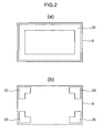
- the pressure sensitive ink layer 30 By forming the pressure sensitive ink layer 30 in a ring shape with a width from 0.2 to 20 mm along the support 2a as shown in FIG. 2a , when pressing force is applied to the protective panel 4, regardless to the pressure applied position, the pressure on the protective panel 4 is applied to the pressure sensitive ink layer 30 and the pressure sensitive ink layer 30 is rendered conductive. This allows pressing force applied to the protective panel 4 to be detected both stably and reliably.
- the resistance value changes based on the size of the pressing force.
- the materials used to make the pressure sensitive ink layer 30 can be one or more metals, other conductive or semiconductive elements and oxides, and conductive or semiconductive organic or inorganic polymers. Specific examples include one or more metals such as titanium, tantalum, zirconium, vanadium, niobium, hafnium, aluminum, silicon, tin, chromium, molybdenum, tungsten, lead, manganese, beryllium, iron, cobalt, nickel, platinum, palladium, osmium, iridium, rhenium, technetium, rhodium, ruthenium, gold, silver, cadmium, copper, zinc, germanium, arsenic, antimony, bismuth, boron, scandium, as well as lanthanides and actinides.
- metals such as titanium, tantalum, zirconium, vanadium, niobium, hafnium, aluminum, silicon, tin, chromium, moly
- Conductive fillers can be used if the basic elements are in a non-oxidized state. Powders, grains, and fibers of conductive materials can be used. Spheres with a diameter from 0.04 to 0.2 ⁇ m are preferred. The amount dispersed should be adjusted based on the desired pressure sensitivity.
- the binder in the pressure sensitive ink layer 30 is a resin whose glass transition point (Tg) is higher than room temperature.
- Specific examples include vinyl hydrochloride/vinyl acetate copolymer resins, acrylic resins, polyurethane resins, polyester resins, epoxy resins, chlorinated polyolefins, nitrocellulose resins, ethyl cellulose resins, polyamide resins, and photocurable resins.
- quantum tunneling composites have superior performance as materials in pressure sensitive ink layers 30.
- the pressure sensitive ink layer 30 can be formed directly on the periphery of the backside of the protective panel 4 using, for example, screen printing, a roll coater method, or a dispenser method.
- the pressure sensitive ink layer 30 is formed on the base film 31 using any printing method common in the art such as screen printing, offset printing, gravure printing, or flexographic printing; and the transparent resin film 31 on which the pressure sensitive ink layer 30 has been formed is applied to the backside of the protective panel 4 using a printing method suitable for mass production such as the roll to roll (R-to-R) method.
- the base film 31 on which the pressure sensitive ink layer 30 has been formed covers the entire backside of the protective panel, the cable for the protective panel 4 mentioned above is installed after the panel has been affixed.
- the base film 31 on which the pressure sensitive ink layer 30 has been formed and which is itself affixed to the backside of the protective panel 4 can be a polycarbonate, polyamide, or polyether-ketone engineering plastic; or an acrylic, polyethylene terephthalate, or polybutylene terephthalate transparent film.
- the thickness of the pressure sensitive ink layer 30 is from 1 to 200 ⁇ m. If the thickness exceeds 200 ⁇ m, a printing layer cannot be formed, and the layer cannot be applied to products requiring thinness such as mobile devices. The pressure detecting characteristics of the pressure sensitive ink layer 30 are uneven if the thickness is less than 1 ⁇ m.
- a connector 18 connected to a control unit 20 inside the case 2 is disposed at the end of a lead wire 17 such as an FPC extending from the electrodes 16a, 16b ( FIG. 1b ).
- the control unit 20 determines that pressure has been applied to the protective panel 4 when the input load applied to the protective panel 4 transmitted via the connector 18 exceeds a threshold value. More specifically, the control unit 20 determines that pressure has been applied to the protective panel 4 when the resistance value between the pair of electrodes 16a, 16b transmitted via the connector 18 falls below a predetermined threshold value.
- the pair of electrodes 16a, 16b can be linear, as shown in FIG. 3a .
- the pair of electrodes 16a, 16b can be comb-shaped.
- the comb-shaped electrodes can be ring-shaped, with teeth thereof meshed with each other, so as to surround the opening 7 ( FIG. 3b ). Because the projected area of the electrodes 16a, 16b on the pressure sensitive ink layer 30 is greater in this configuration, contact is readily established between the pressure sensitive ink layer 30 and the electrodes 16a, 16b, and they are readily rendered conductive when pressure is applied to the pressure sensor 40. This can improve pressure sensitivity.
- the electrodes 16a, 16b can be comb-shaped only in the corner portions corresponding to the areas in which the pressure sensitive ink layer 30 is formed.
- the surface of the electrodes 16 can be covered with a carbon layer 50 ( FIG. 5 ).
- the electrode 16a arranged on the upper film 6 was covered with the pressure sensitive ink layer 30, and the electrode 16b arranged on the base film 31 was covered with a carbon layer 50.
- the electrode 16b can be protected by being coated with the carbon layer 50.
- the spacer 10 was interposed between the pair of electrodes 16a, 16b in the vertical direction.
- the present invention is not restricted to this embodiment.
- the pair of electrodes 16a, 16b can be arranged on the base film 31 ( FIG. 6 ).
- the pressure sensitive ink layer 30 is arranged in certain locations so as to be able cover both electrodes 16a, 16b. Because the pair of electrodes can be arranged side by side on the base film in this configuration, the thickness of the pressure sensor can be reduced.
- the pair of electrodes 16a, 16b can also be covered with a carbon layer 50 ( FIG. 7 ).
- Aluminum hydroxide powder with an average particle size of 27 ⁇ m was added to pure water to prepare a slurry with a 45% powder concentration.
- the slurry was sprayed at a rate of 14 kg/h from the center of a two-fluid nozzle into the flames of a combustion furnace using oxygen gas with a gauge pressure of 0.2 MPa and a flow rate of approximately 12 Nm 3 /h.
- From the burner was sprayed a gas mixture of 5 Nm 3 /h LPG and 7 Nm 3 /h oxygen gas for the inner flame, and from the outermost peripheral space of the burner was sprayed a gas mixture of 4 Nm 3 /h LPG and 13 Nm 3 /h oxygen gas for the outer flame.
- the alumina powder recovered from the cyclone furnace was measured using a laser diffraction scattering-type particle size distribution measuring device. The sphericity was 0.95, and the average particle size was 48 ⁇ m.
- An addition reaction silicone resin (Dow Corning Toray SE1885) and the alumina powder manufactured using the aforementioned method were mixed together to produce a resin composition.
- the resulting resin composition was vacuum-degassed at room temperature, and a doctor blade method was used to form a 5 ⁇ m sheet.
- the resulting sheet was allowed to stand for five hours in a dryer at 150°C, where it was vulcanized and cured to produce a spacer.
- the spacer manufactured as described above was cut to a size of 25 mm by 100 mm, affixed to commercially available PET film, and subjected to 20 N of pressing force.
- the PET film was stretched in the 180° direction at a rate of 10 mm/min. using a tensile strength testing device, and the 180° peel strength was measured.
- the measurement result was low; i.e., 0.008 N, but an adhesive property was evident.
- Pressure sensitive ink consisting of a quantum tunneling composite (QTC from Peratech (U.K.) was formed into a 10- ⁇ m-thick, 3-mm-wide loop shape on top of polycarbonate using the screen printing method, and the polycarbonate film on which this pressure sensitive ink layer had been formed was affixed to the backside of a protective panel.
- QTC quantum tunneling composite
- a pair of comb-shaped electrodes was formed on top of a polyester film, and the polycarbonate film affixed to the backside of the protective panel was disposed on top of the polyester film.
- the adhesive spacer was then disposed to oppose the pressure sensitive ink layer on the surface of the comb-shaped electrodes formed on top of the polyester film.
- the pressure detection operation was then confirmed after leaving the protective panel in a high-temperature environment (85°C) for 16 hours. As a result, hardly any change in the F-R characteristics was observed after the panel had been placed in the high-temperature environment. Also, there was no expansion of the pressure sensitive ink layer in the high-temperature environment. As a result, the sensitivity did not decrease, and there was no adverse connection with the electrodes.
- the configuration was similar to that of the first example except that the pressure sensitive ink layer 30 was disposed on the bottom surface of the upper film 6 in the portions corresponding to the corner portions on the backside periphery of the protective panel 4, and the protective panel 4 functioned as a cross switch.
- the results were similar to the first example.
- the configuration was similar to the first example except that the pair of electrodes 16a, 16b was spiral shaped.
- the results were similar to the first example.
- the pair of electrodes 16a, 16b is spiral shaped, the projected area of the electrodes 16a, 16b towards the pressure sensitive ink layer 30 is larger.
- the pressure sensitive ink layer 30 readily makes contact with the electrodes 16a, 16b, and can readily be rendered conductive. In this way, pressure sensitivity can be improved.
- the pair of electrodes 16a, 16b correspond to the portions in which a pressure sensitive ink layer 30 has been formed, and form a spiral shape only in the corner portions.
- the present invention can be used in a pressure sensor for measuring the pressure distribution in a component perpendicular to a surface when external pressure has been applied to the surface.
Landscapes
- Physics & Mathematics (AREA)
- General Physics & Mathematics (AREA)
- Push-Button Switches (AREA)
- Force Measurement Appropriate To Specific Purposes (AREA)
Abstract
Description
- The present invention relates to a pressure sensor for measuring the pressure distribution in a component perpendicular to a surface when external pressure has been applied to the surface.
- An example of a configuration of a pressure sensor for distributing external pressure applied to a surface is described in Patent Literature 1. In one of these sensors, as shown in
FIG. 1 of Patent Literature 1, two sheets of film are separated by a spacer to form an air layer, an upper electrode is disposed on the upper film, a lower electrode is disposed on the lower film, and a pressure sensitive ink layer is disposed between the two. - When pressure is applied to the upper film, the upper electrode and the lower electrode are rendered conductive in the vertical direction in the portion sustaining the pressure, output is obtained only in the lower electrode corresponding to the intersection, and the pressure distribution is outputted. When a pressure sensor is disposed inside a vehicle seat, it can be determined whether a passenger is sitting on the seat, and the physical attributes of the passenger can be determined from the pressure distribution.
- In the pressure sensor disclosed in Patent Literature 1, a spacer is disposed to create an air layer between the upper film and the lower film. When pressure is applied, the electrodes make contact via a pressure sensitive ink layer, and the pressure is measured from the change in the resistance value based on the pressure applied to the pressure sensitive ink layer.
- However, when the film deteriorates over time due to use, the upper film sags and it becomes difficult to control contact between the pressure sensitive ink layer and the electrodes based on the load. Because of this, the reproducibility of the resistance value between the pressure sensitive ink layer and the electrodes due to a load is low, and the pressure is difficult to measure with precision. Also, because this pressure sensor is configured so that electrodes are disposed in most of the film surface, the transparency of the pressure sensor is poor.
- In order to solve this problem, the applicant filed a patent application for a pressure sensor having a configuration in which a pair of electrodes is disposed on the lower film, and the pair of electrodes is covered with a pressure sensitive conductive ink layer. In this pressure sensor, because a pair of electrodes is disposed on the lower film, and the pressure sensitive conductive ink layer disposed on the upper film normally covers the electrodes, a spacer does not have to be disposed to form an air layer. As a result, the sensor can assume any shape based on the arrangement of the electrodes. By configuring the pair of electrodes in the shape of a frame, the central portion of the pressure sensor can be transparent. This enables a touch panel to be disposed in this portion.
-
- [Patent Literature 1] Japanese Laid-open Patent Publication No.
2002-48658 - However, in a pressure sensor with this configuration, because a small load results in a small change in the resistance value of the pressure sensitive conductive ink layer, the amount of current flowing between the pressure sensitive conductive ink layer and the electrodes remains nearly constant, and pressure detection is difficult to perform with precision.
- Since the pair of electrodes remain conductive even when no load is applied, power is consumed unnecessarily.
- Therefore, the technical problem that the present invention is intended to resolve is to provide a pressure sensor that can overcome the aforedescribed problems, detect pressure even when there is a small load, and eliminate unnecessary power consumption.
- In order to solve this technical problem, the present invention provides a pressure sensor having the following configuration.
- A first aspect of the present invention comprises a pair of electrodes; a base film on which at least one electrode is arranged; an upper film facing the base film; a pressure sensitive ink layer arranged so as to be able to cover the pair of electrodes and having electrical characteristics that change under an applied pressing force; and an adhesive spacer interposed between the base film and the upper film.
- According to the aspect described above, a pair of electrodes and a pressure sensitive ink layer can be disposed between the base film and the upper film. A spacer having adhesive properties is interposed between the base film and the upper film. Thus, the spacer can be disposed between the pair of electrodes and the pressure sensitive ink layer. Here, the pressure sensitive ink layer and the pair of electrodes are usually separated by the spacer. Even when the upper film sags over time, direct contact is not made between the pressure sensitive ink layer and the pair of electrodes due to the adhesive spacer. As a result, the electrodes are not rendered conductive via the pressure sensitive ink layer.
When compressive pressure is applied, the pressure sensitive ink layer and the pair of electrodes readily make contact, and the electrodes are rendered conductive via the pressure sensitive ink layer. Therefore, the resistance value between the pressure sensitive ink layer and the electrodes can be controlled based on the load, and even low loads are sensed reliably. Because the pressure sensitive ink layer and the pair of electrodes remain laminated due to the adhesiveness of the spacer, the laminating step and assembly step can be performed efficiently. - According to a second aspect of the present invention, the spacer is vertically interposed between the pair of electrodes.
- Because the pair of electrodes is disposed vertically in this configuration, an electrode can be disposed, respectively, on the base film and the upper film. In this configuration, the pair of electrodes and the spacer are disposed in the direction of the pressure when compressive pressure is applied. As a result, the pressure sensitive ink layer and the pair of electrodes are able to make contact reliably when pressed down.
- According to a third aspect of the present invention, the pair of electrodes is arranged on the base film.
- Because the pair of electrodes can be placed side by side on the base film in this configuration, the thickness of the pressure sensor can be reduced.
- According to a fourth aspect of the present invention, the spacer contains a filler having a sphericity of 0.85 to 0.98, and an average particle size of 3 to 40 µm.
- Because the adhesiveness of the spacer is set to the proper amount in this configuration, the sensing can be performed more reliably.
- According to a fifth aspect of the present invention, a material used for the spacer is an addition-reaction-type liquid silicone resin.
- Because the spacer is sufficiently flexible and elastic, and also has adhesive properties, it reliably transmits pressing force and performs sensing more reliably even when the load is low.
- According to a sixth aspect of the present invention, the electrodes are covered with carbon.
- In the aspect described above, the electrodes can be protected by a coating of carbon.
-
-
FIG. 1 is a cross-sectional view showing the configuration of a pressure sensor of the present invention; -
FIG. 2 is (a) a top view showing the configuration of the pressure sensor, and (b) a top view showing a variation on the pressure sensitive ink layer shown in (a); -
FIG. 3 is (a) a top view showing the configuration of the pressure sensor, (b) a top view showing a variation on the pair of electrodes shown in (a), and (c) a top view showing a second variation on the pair of electrodes shown in (a); -
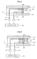
FIG. 4 is a schematic view showing the pressure sensitive ink layer disposed on only one electrode; -
FIG. 5 is a schematic view showing the surface of one electrode coated with a carbon layer; -
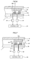
FIG. 6 is a cross-sectional view showing the configuration of the pressure sensor in another embodiment; and -
FIG. 7 is a schematic view showing the surface of electrodes coated with a carbon layer in the pressure sensor of another embodiment. - The following is an description of examples of the present invention made with reference to the accompanying drawings.
- Pressure sensors are incorporated into electronic devices such as cellular telephones, smart phones, PDAs, car navigation devices, digital cameras, digital video cameras, and gaming devices. In this embodiment, the electronic device is a cellular telephone.
- As shown in
FIG. 1 , a cellular telephone 1 includes acase 2 made of a synthetic resin, adisplay device 3 having a display unit of, for example, liquid crystals or organic EL disposed in thecase 2, apressure sensor 40 disposed on top of thedisplay device 3, and aprotective panel 4 disposed on top of thepressure sensor 40. Theprotective panel 4 and thepressure sensor 40 are housed in a recess in thecase 2 formed where thedisplay device 3 is installed, and the upper surface of thecase 2 conforms substantially to the upper surface of theprotective panel 4. - The
protective panel 4 has a rectangular shape when viewed from above. The upper surface of theprotective panel 4 allows the display unit in thedisplay device 3 to be viewed from the outside. Theprotective panel 4 also includes atransparent display window 8 formed so as to correspond to the display unit, and adecorative portion 9 formed on the periphery of thedisplay unit 8 and able to conceal what is inside. Theprotective panel 4 has a "touch input function" able to detect the X-Y coordinates of the operated position based on a touch operation performed on theprotective panel 4. However, selection does not have to be performed using a touch input function. The resistance film method, the electrostatic capacitance method, or the electromagnetic induction method can be used to make selections when a touch input function is installed. - The
pressure sensor 40 includes a pair ofelectrodes base film 31 on which at least one electrode is disposed,upper film 6 facing thebase film 31, a pressuresensitive ink layer 30 disposed so as to be able to cover the pair ofelectrodes spacer 10 having adhesive properties and interposed between thebase film 31 and theupper film 6. - In this configuration, the pair of
electrodes sensitive ink layer 30 can be disposed between thebase film 31 and theupper film 6. Thespacer 10 is interposed between thebase film 31 and theupper film 6. As a result, thespacer 10 can be arranged between the pair ofelectrodes sensitive ink layer 30. Here, the pressuresensitive ink layer 30 and the pair ofelectrodes spacer 10. Also, theadhesive spacer 10 keeps the pressuresensitive ink layer 30 from making direct contact with the pair ofelectrodes upper film 6 begins to sag over time. When pressing force is applied, the pressuresensitive ink layer 30 readily comes into contact with the pair ofelectrodes sensitive ink layer 30, and the resistance value between the pressuresensitive ink layer 30 and the electrodes can be controlled based on the load. - In this embodiment, the
spacer 10 is interposed vertically between the pair ofelectrodes electrodes base film 31 and theupper film 6. - An
opening 7 is formed in thebase film 31 corresponding to thedisplay device 3 and thedisplay window 8. The pair ofelectrodes base film 31 so as to surround theopening 7. The pressuresensitive ink layer 30 is also formed on the bottom surface of theupper film 6 in ring shape in order to cover the pair ofelectrodes opening 7. - Examples of materials that can be used in a
spacer 10 with adhesive properties include epoxyacrylate and urethane acrylate photocuring resins, and silicone, polyester and epoxy thermoset resins. Among these, an addition-reaction-type liquid silicone having flexible and elastic properties is preferred. - Specific examples of addition-reaction-type liquid silicones include a one-part liquid silicone having both a vinyl group and H-Si group in the molecule, and a two-part liquid silicone solution having two or more terminal or side chain H-Si groups.
- The
spacer 10 preferably contains a filler. One example of a filler is a spherical alumina powder with an average particle size of several tens of microns. This alumina powder can be manufactured using any desired method. However, the flame spraying method using aluminum hydroxide powder is preferred from the standpoint of controlling the particle size distribution and controlling particle shape. The crystal structure of the powder can be either monocrystalline or polycrystalline. The granularity of the powder can be adjusted by classifying and mixing powders. - Preferably, the sphericity of the filler is from 0.85 to 0.98, and the average particle size is from 3 µm to 40 µm (the average particle size should be at least 3 µm even when a single digit or double digit percentage of the particles have a size less than 3 µm). If the sphericity is less than 0.85, the fluidity of the powder deteriorates, and the filler becomes segregated inside the spacer. If the sphericity is greater than 0.98, the density increases, and the adhesive properties tend to be lost when used as a spacer. If the average particle size is less than 3 µm, the adhesiveness deteriorates in the spacer even when the sphericity is sufficient. If more than 15% of the particles have an average particle size less than 1 µm, the adhesiveness of the spacer is also poor, even when the average particle size is greater than 3 µm. If the average particle size is greater than 40 µm, the surface coarseness of the
spacer 10 increases significantly, and the spacer becomes hard and difficult to handle. - If necessary, various types of curing agents and other additives can be compounded in the
spacer 10. By properly compounding curing agents and other additives, the crosslinking density formed by the addition reaction can be adjusted, whereby the flexibility of thespacer 10 can be adjusted. - The thickness of the
spacer 10 ranges from 0.2 to 500 µm, preferably from 0.5 to 100 µm. There are no particular restrictions on the planar shape of thespacer 10, which can be, e.g., polygonal, round, or oval. In order to improve adhesiveness, the coarseness should be in the range of tens of microns. - When the spacer is an addition-reaction-type liquid silicone, the materials can be mixed together using a mixer such as a roll mill, kneader, or Banbury mixer; molded using, e.g., a doctor blade method, extrusion, pressing, or calendering; and then vulcanized at a temperature around 100°C. using, e.g., a hot air dryer, infrared dryer, or microwave dryer to complete the spacer.
- In the case of sphericity, the projected area (S1) and perimeter of a particle in an SEM image are measured, the area of a perfect circle (S2) is calculated based on the perimeter, and S1/S2 indicates the sphericity of the particle. Fifty randomly selected particles are measured in this manner, and the average value is used as the sphericity.
- The adhesiveness is determined using a 180° peel test. The spacer is determined to be adhesive when a load of at least 0.008 N is needed to peel a 25-mm-wide spacer. In addition to the
spacer 10, adhesiveness can be provided in other areas. - The pressure
sensitive ink layer 30 is interposed between a support 2a and the periphery of the backside of theprotective panel 4 with theprotective panel 4 inserted in thecase 2. This allows pressing force applied to theprotective panel 4 to be detected (Z coordinate detection). The pressuresensitive ink layer 30 is configured so as to cover both of theelectrodes FIG. 1 ), or to cover one of theelectrodes FIG. 4 ). - By forming the pressure
sensitive ink layer 30 in a ring shape with a width from 0.2 to 20 mm along the support 2a as shown inFIG. 2a , when pressing force is applied to theprotective panel 4, regardless to the pressure applied position, the pressure on theprotective panel 4 is applied to the pressuresensitive ink layer 30 and the pressuresensitive ink layer 30 is rendered conductive. This allows pressing force applied to theprotective panel 4 to be detected both stably and reliably. - In an analog pressure
sensitive ink layer 30, the resistance value changes based on the size of the pressing force. - The materials used to make the pressure
sensitive ink layer 30 can be one or more metals, other conductive or semiconductive elements and oxides, and conductive or semiconductive organic or inorganic polymers. Specific examples include one or more metals such as titanium, tantalum, zirconium, vanadium, niobium, hafnium, aluminum, silicon, tin, chromium, molybdenum, tungsten, lead, manganese, beryllium, iron, cobalt, nickel, platinum, palladium, osmium, iridium, rhenium, technetium, rhodium, ruthenium, gold, silver, cadmium, copper, zinc, germanium, arsenic, antimony, bismuth, boron, scandium, as well as lanthanides and actinides. One or more conductive agents can also be used as appropriate. Conductive fillers can be used if the basic elements are in a non-oxidized state. Powders, grains, and fibers of conductive materials can be used. Spheres with a diameter from 0.04 to 0.2 µm are preferred. The amount dispersed should be adjusted based on the desired pressure sensitivity. - The binder in the pressure
sensitive ink layer 30 is a resin whose glass transition point (Tg) is higher than room temperature. Specific examples include vinyl hydrochloride/vinyl acetate copolymer resins, acrylic resins, polyurethane resins, polyester resins, epoxy resins, chlorinated polyolefins, nitrocellulose resins, ethyl cellulose resins, polyamide resins, and photocurable resins. Among these, quantum tunneling composites have superior performance as materials in pressure sensitive ink layers 30. - The pressure
sensitive ink layer 30 can be formed directly on the periphery of the backside of theprotective panel 4 using, for example, screen printing, a roll coater method, or a dispenser method. Preferably, the pressuresensitive ink layer 30 is formed on thebase film 31 using any printing method common in the art such as screen printing, offset printing, gravure printing, or flexographic printing; and thetransparent resin film 31 on which the pressuresensitive ink layer 30 has been formed is applied to the backside of theprotective panel 4 using a printing method suitable for mass production such as the roll to roll (R-to-R) method. When thebase film 31 on which the pressuresensitive ink layer 30 has been formed covers the entire backside of the protective panel, the cable for theprotective panel 4 mentioned above is installed after the panel has been affixed. - The
base film 31 on which the pressuresensitive ink layer 30 has been formed and which is itself affixed to the backside of theprotective panel 4 can be a polycarbonate, polyamide, or polyether-ketone engineering plastic; or an acrylic, polyethylene terephthalate, or polybutylene terephthalate transparent film. - The thickness of the pressure
sensitive ink layer 30 is from 1 to 200 µm. If the thickness exceeds 200 µm, a printing layer cannot be formed, and the layer cannot be applied to products requiring thinness such as mobile devices. The pressure detecting characteristics of the pressuresensitive ink layer 30 are uneven if the thickness is less than 1 µm. - A
connector 18 connected to acontrol unit 20 inside thecase 2 is disposed at the end of alead wire 17 such as an FPC extending from theelectrodes FIG. 1b ). Thecontrol unit 20 determines that pressure has been applied to theprotective panel 4 when the input load applied to theprotective panel 4 transmitted via theconnector 18 exceeds a threshold value. More specifically, thecontrol unit 20 determines that pressure has been applied to theprotective panel 4 when the resistance value between the pair ofelectrodes connector 18 falls below a predetermined threshold value. - The pair of
electrodes FIG. 3a . Or the pair ofelectrodes FIG. 3b ). Because the projected area of theelectrodes sensitive ink layer 30 is greater in this configuration, contact is readily established between the pressuresensitive ink layer 30 and theelectrodes pressure sensor 40. This can improve pressure sensitivity. When the pressuresensitive ink layer 30 is formed only in the corner portions as shown inFIG. 2b , theelectrodes sensitive ink layer 30 is formed. - The surface of the electrodes 16 can be covered with a carbon layer 50 (
FIG. 5 ). InFIG. 5 , theelectrode 16a arranged on theupper film 6 was covered with the pressuresensitive ink layer 30, and theelectrode 16b arranged on thebase film 31 was covered with acarbon layer 50. In this configuration, theelectrode 16b can be protected by being coated with thecarbon layer 50. - In the embodiment described above, the
spacer 10 was interposed between the pair ofelectrodes electrodes FIG. 6 ). Here, the pressuresensitive ink layer 30 is arranged in certain locations so as to be able cover bothelectrodes - The pair of
electrodes FIG. 7 ). - The following is a more detailed explanation of the present invention with reference to examples and comparative examples.
- Aluminum hydroxide powder with an average particle size of 27 µm was added to pure water to prepare a slurry with a 45% powder concentration. The slurry was sprayed at a rate of 14 kg/h from the center of a two-fluid nozzle into the flames of a combustion furnace using oxygen gas with a gauge pressure of 0.2 MPa and a flow rate of approximately 12 Nm3/h. From the burner was sprayed a gas mixture of 5 Nm3/h LPG and 7 Nm3/h oxygen gas for the inner flame, and from the outermost peripheral space of the burner was sprayed a gas mixture of 4 Nm3/h LPG and 13 Nm3/h oxygen gas for the outer flame. The alumina powder recovered from the cyclone furnace was measured using a laser diffraction scattering-type particle size distribution measuring device. The sphericity was 0.95, and the average particle size was 48 µm.
- An addition reaction silicone resin (Dow Corning Toray SE1885) and the alumina powder manufactured using the aforementioned method were mixed together to produce a resin composition. The resulting resin composition was vacuum-degassed at room temperature, and a doctor blade method was used to form a 5 µm sheet. The resulting sheet was allowed to stand for five hours in a dryer at 150°C, where it was vulcanized and cured to produce a spacer.
- The spacer manufactured as described above was cut to a size of 25 mm by 100 mm, affixed to commercially available PET film, and subjected to 20 N of pressing force. The PET film was stretched in the 180° direction at a rate of 10 mm/min. using a tensile strength testing device, and the 180° peel strength was measured. The measurement result was low; i.e., 0.008 N, but an adhesive property was evident.
- Pressure sensitive ink consisting of a quantum tunneling composite (QTC from Peratech (U.K.)) was formed into a 10-µm-thick, 3-mm-wide loop shape on top of polycarbonate using the screen printing method, and the polycarbonate film on which this pressure sensitive ink layer had been formed was affixed to the backside of a protective panel.
- A pair of comb-shaped electrodes was formed on top of a polyester film, and the polycarbonate film affixed to the backside of the protective panel was disposed on top of the polyester film. The adhesive spacer was then disposed to oppose the pressure sensitive ink layer on the surface of the comb-shaped electrodes formed on top of the polyester film.
- Pressure was applied with the tip of a R 0.8 polyacetal pen to the surface of the protective panel in this configuration, and the change in the resistance value was measured. The resistance of the pressure sensitive ink layer gradually decreased as the pen input load increased between 0 and 2 N (approximately 200 gf). In this measurement, it was clear that the pen input load could be detected based on the change in the resistance value.
- The pressure detection operation was then confirmed after leaving the protective panel in a high-temperature environment (85°C) for 16 hours. As a result, hardly any change in the F-R characteristics was observed after the panel had been placed in the high-temperature environment. Also, there was no expansion of the pressure sensitive ink layer in the high-temperature environment. As a result, the sensitivity did not decrease, and there was no adverse connection with the electrodes.
- As shown in
FIG. 2b , the configuration was similar to that of the first example except that the pressuresensitive ink layer 30 was disposed on the bottom surface of theupper film 6 in the portions corresponding to the corner portions on the backside periphery of theprotective panel 4, and theprotective panel 4 functioned as a cross switch. The results were similar to the first example. - As shown in
FIG. 3c , the configuration was similar to the first example except that the pair ofelectrodes electrodes electrodes sensitive ink layer 30 is larger. Thus, when pressure is applied to thepressure sensor 40, the pressuresensitive ink layer 30 readily makes contact with theelectrodes sensitive ink layer 30 is formed only in the corner portions as inFIG. 2b , the pair ofelectrodes sensitive ink layer 30 has been formed, and form a spiral shape only in the corner portions. - The present invention can be used in a pressure sensor for measuring the pressure distribution in a component perpendicular to a surface when external pressure has been applied to the surface.
-
- 1
- Cellular telephone
- 2
- Case
- 3
- Display device
- 4
- Protective panel
- 6
- Upper film
- 7
- Opening
- 8
- Display window
- 9
- Decorative portion
- 10
- Spacer
- 16a, 16b
- Electrodes
- 17
- Lead wire
- 18
- Connector
- 20
- Control unit
- 30
- Pressure sensitive ink layer
- 31
- Base film
- 40
- Pressure Sensor
- 50
- Carbon layer
Claims (6)
- A pressure sensor characterized by:a pair of electrodes;a base film on which at least one electrode is arranged;an upper film facing the base film;a pressure sensitive ink layer arranged so as to be able to cover the pair of electrodes and having electrical characteristics that change under an applied pressing force; andan adhesive spacer interposed between the base film and the upper film.
- The pressure sensor according to claim 1, characterized in that the spacer is vertically interposed between the pair of electrodes.
- The pressure sensor according to claim 1, characterized in that the pair of electrodes is arranged on the base film.
- The pressure sensor according to any of claims 1 through 3, characterized in that the spacer contains a filler having a sphericity of 0.85 to 0.98, and an average particle size of 3 to 40 µm.
- The pressure sensor according to any of claims 1 through 4, characterized in that a material used for the spacer is an addition-reaction-type liquid silicone resin.
- The pressure sensor according to any of claims 1 through 5, characterized in that the electrodes are covered with carbon.
Applications Claiming Priority (2)
| Application Number | Priority Date | Filing Date | Title |
|---|---|---|---|
| JP2008249688 | 2008-09-29 | ||
| PCT/JP2009/065308 WO2010035615A1 (en) | 2008-09-29 | 2009-09-02 | Pressure sensor |
Publications (2)
| Publication Number | Publication Date |
|---|---|
| EP2330395A1 true EP2330395A1 (en) | 2011-06-08 |
| EP2330395A4 EP2330395A4 (en) | 2015-12-23 |
Family
ID=42059621
Family Applications (1)
| Application Number | Title | Priority Date | Filing Date |
|---|---|---|---|
| EP09816032.8A Withdrawn EP2330395A4 (en) | 2008-09-29 | 2009-09-02 | Pressure sensor |
Country Status (7)
| Country | Link |
|---|---|
| US (1) | US20110198712A1 (en) |
| EP (1) | EP2330395A4 (en) |
| JP (1) | JP4824831B2 (en) |
| KR (1) | KR101255451B1 (en) |
| CN (1) | CN102165298B (en) |
| TW (1) | TWI475199B (en) |
| WO (1) | WO2010035615A1 (en) |
Families Citing this family (17)
| Publication number | Priority date | Publication date | Assignee | Title |
|---|---|---|---|---|
| JP2011047893A (en) * | 2009-08-28 | 2011-03-10 | Nissha Printing Co Ltd | Pressure detection unit |
| JP5546327B2 (en) * | 2010-04-12 | 2014-07-09 | 日本写真印刷株式会社 | Information input device |
| JP5202578B2 (en) * | 2010-06-03 | 2013-06-05 | 日本写真印刷株式会社 | Information detector including pressure detector and pressure detector |
| US20120092294A1 (en) | 2010-10-18 | 2012-04-19 | Qualcomm Mems Technologies, Inc. | Combination touch, handwriting and fingerprint sensor |
| TW201326773A (en) | 2011-12-30 | 2013-07-01 | Ind Tech Res Inst | Adjustment apparatus for pressure sensor and adjustment method thereof |
| US9024910B2 (en) | 2012-04-23 | 2015-05-05 | Qualcomm Mems Technologies, Inc. | Touchscreen with bridged force-sensitive resistors |
| US10131127B2 (en) * | 2012-06-15 | 2018-11-20 | Tufts University | Paint-on approach for fabrication of electrically active structures |
| JP5699111B2 (en) * | 2012-07-19 | 2015-04-08 | 日本写真印刷株式会社 | Resistive touch panel and touch panel device |
| TWI629459B (en) * | 2013-02-06 | 2018-07-11 | 藤倉股份有限公司 | Method for manufacturing pressure detecting device, pressure detecting device, pressure detecting device and electronic device |
| KR20150038988A (en) * | 2013-10-01 | 2015-04-09 | 삼성전기주식회사 | Touch sensor |
| DE102014221838B3 (en) * | 2014-10-27 | 2016-03-24 | Volkswagen Aktiengesellschaft | NiTi sensor device for detecting parameters of a motor vehicle occupant |
| US20180067602A1 (en) * | 2015-03-30 | 2018-03-08 | Rohm And Haas Electronic Materials Llc | Transparent pressure sensing film composition |
| CN105049511B (en) * | 2015-07-29 | 2018-04-10 | 浙江大学 | A kind of pressure distributed sensor and its intelligent sick bed monitoring system and monitoring method |
| JP6297613B2 (en) * | 2016-03-22 | 2018-03-20 | Nissha株式会社 | Pressure sensor |
| KR101734856B1 (en) * | 2016-11-14 | 2017-05-25 | 주식회사 올아이티탑 | Certification card checking fingerprint and sensing a henatocele of finger |
| CN108362365A (en) * | 2018-01-18 | 2018-08-03 | 英华达(上海)科技有限公司 | The method of batheroom scale and its identification user with identification user function |
| LT6804B (en) | 2019-07-17 | 2021-03-10 | VšĮ Vilniaus Gedimino technikos universitetas | Universal pressure, compressive force and stress sensor |
Family Cites Families (29)
| Publication number | Priority date | Publication date | Assignee | Title |
|---|---|---|---|---|
| US3314814A (en) * | 1964-03-02 | 1967-04-18 | Columbia Ribbon & Carbon | Method of preparing transfer elements |
| US4315238A (en) * | 1979-09-24 | 1982-02-09 | Eventoff Franklin Neal | Bounceless switch apparatus |
| JPH0629801B2 (en) * | 1985-11-15 | 1994-04-20 | 東芝シリコ−ン株式会社 | Keystroke sensor- |
| US4794366A (en) * | 1985-11-15 | 1988-12-27 | Toshiba Silicone Co., Ltd. | Key-touch sensor and method of manufacture |
| US5695859A (en) * | 1995-04-27 | 1997-12-09 | Burgess; Lester E. | Pressure activated switching device |
| DE69716332T2 (en) * | 1996-04-15 | 2003-02-20 | Teijin Seiki Co. Ltd., Osaka | Use of a photo-curable resin composition for producing an object by means of stereolithography |
| JPH10325763A (en) * | 1997-05-24 | 1998-12-08 | Tomohiko Yara | Pressurization sensor |
| JP2000283866A (en) * | 1999-01-27 | 2000-10-13 | Furukawa Electric Co Ltd:The | Film pressure sensor |
| JP2000314665A (en) * | 1999-05-06 | 2000-11-14 | Furukawa Electric Co Ltd:The | Film sensor |
| JP3787717B2 (en) * | 1999-12-28 | 2006-06-21 | ニッタ株式会社 | Pressure-sensitive conductive ink composition |
| JP2002048658A (en) | 2000-08-07 | 2002-02-15 | Polymatech Co Ltd | Pressure distribution detecting device |
| JP4574885B2 (en) * | 2001-03-29 | 2010-11-04 | 電気化学工業株式会社 | Heat dissipation spacer |
| JP4634649B2 (en) * | 2001-06-01 | 2011-02-16 | 株式会社フジクラ | Membrane switch and pressure sensor |
| KR100504570B1 (en) * | 2001-12-27 | 2005-08-04 | 엘지.필립스 엘시디 주식회사 | Touch Panel and Fabricating Method of Dot Spacer Thereof |
| KR100559153B1 (en) * | 2002-02-28 | 2006-03-10 | 히다치 가세고교 가부시끼가이샤 | Method for connecting electrodes, surface-treated wiring board and adhesive film used in the method, and electrodes-connected structure |
| JP2004028883A (en) * | 2002-06-27 | 2004-01-29 | Denso Corp | Pressure sensor |
| JP2004037350A (en) * | 2002-07-05 | 2004-02-05 | Nitta Ind Corp | Resistive sensor |
| US7541128B2 (en) * | 2002-09-26 | 2009-06-02 | Ricoh Company Limited | Toner, developer including the toner, and method for fixing toner image |
| JP3986985B2 (en) * | 2003-03-25 | 2007-10-03 | 株式会社デンソー | Pressure-sensitive resistor and pressure-sensitive sensor |
| US7785704B2 (en) * | 2003-05-14 | 2010-08-31 | Tekscan, Inc. | High temperature pressure sensitive devices and methods thereof |
| GB0407366D0 (en) * | 2004-03-31 | 2004-05-05 | Koninkl Philips Electronics Nv | Textile form touch sensor |
| US7703342B2 (en) * | 2005-03-30 | 2010-04-27 | Xiroku, Inc. | Pressure distribution detection device |
| JP2006317340A (en) * | 2005-05-13 | 2006-11-24 | Fujikura Ltd | Load sensor |
| JP4533801B2 (en) * | 2005-05-31 | 2010-09-01 | ニッタ株式会社 | Resistive sensor |
| JP3917632B2 (en) * | 2005-10-19 | 2007-05-23 | 株式会社テクノスジャパン | Air adjustment mechanism of load detection sensor |
| JP2008256470A (en) * | 2007-04-03 | 2008-10-23 | Nitta Ind Corp | Pressure distribution sensor system |
| JP4168078B1 (en) * | 2007-07-26 | 2008-10-22 | ニッタ株式会社 | Sensor sheet |
| EP2071312B1 (en) * | 2007-12-13 | 2015-09-16 | Yamaha Corporation | Pressure sensor and data input apparatus |
| TWI388813B (en) * | 2009-08-31 | 2013-03-11 | Universal Cement Corp | Pressure sensor and boxing machine using the same |
-
2009
- 2009-09-02 EP EP09816032.8A patent/EP2330395A4/en not_active Withdrawn
- 2009-09-02 JP JP2010530802A patent/JP4824831B2/en not_active Expired - Fee Related
- 2009-09-02 US US13/120,509 patent/US20110198712A1/en not_active Abandoned
- 2009-09-02 WO PCT/JP2009/065308 patent/WO2010035615A1/en not_active Ceased
- 2009-09-02 KR KR1020117009706A patent/KR101255451B1/en not_active Expired - Fee Related
- 2009-09-02 CN CN2009801381898A patent/CN102165298B/en not_active Expired - Fee Related
- 2009-09-24 TW TW098132315A patent/TWI475199B/en not_active IP Right Cessation
Non-Patent Citations (1)
| Title |
|---|
| See references of WO2010035615A1 * |
Also Published As
| Publication number | Publication date |
|---|---|
| CN102165298A (en) | 2011-08-24 |
| TW201027054A (en) | 2010-07-16 |
| TWI475199B (en) | 2015-03-01 |
| KR20110073546A (en) | 2011-06-29 |
| JPWO2010035615A1 (en) | 2012-02-23 |
| KR101255451B1 (en) | 2013-04-17 |
| EP2330395A4 (en) | 2015-12-23 |
| US20110198712A1 (en) | 2011-08-18 |
| WO2010035615A1 (en) | 2010-04-01 |
| CN102165298B (en) | 2013-10-02 |
| JP4824831B2 (en) | 2011-11-30 |
Similar Documents
| Publication | Publication Date | Title |
|---|---|---|
| US20110198712A1 (en) | Pressure Sensor | |
| TWI475200B (en) | Pressure sensitive sensor | |
| Kim et al. | Skin‐like Omnidirectional Stretchable Platform with Negative Poisson's Ratio for Wearable Strain–Pressure Simultaneous Sensor | |
| US8243225B2 (en) | Electronic device having protection panel | |
| CN101859216B (en) | Touch screen | |
| KR102456154B1 (en) | Sensor, touch sensor and display device | |
| EP2689431B1 (en) | Pressure sensitive polymer composite material adapted for touch screen | |
| CN101436111B (en) | Force imaging input device and system | |
| US20090065267A1 (en) | Input apparatus | |
| EP2485125A1 (en) | Mounting structure for touch input device equipped with a pressure sensor | |
| US20110273394A1 (en) | Methods and apparatus for a transparent and flexible force-sensitive touch panel | |
| KR101210937B1 (en) | Pressure Sensitive Device And Tactile Sensors Using The Same | |
| US20110227836A1 (en) | Transparent force sensor and method of fabrication | |
| US6791532B2 (en) | Input device and detection device using resistance type strain sensor element | |
| JPWO2014157627A1 (en) | Capacitance type sensor sheet and capacitance type sensor | |
| CN105849677A (en) | Electronic device and electronic device control method | |
| WO2011152127A1 (en) | Pressure detection unit and information input device provided with the pressure detection unit | |
| WO2014013807A1 (en) | Resistance film type touch panel and touch panel apparatus | |
| CN212658366U (en) | Flexible pressure sensor and array type pressure detection device | |
| CN107562245A (en) | Touch display unit and electronic equipment | |
| JP7413480B1 (en) | Input device using film-type force sensor and its load detection method | |
| Huang et al. | Two types of flexible tactile sensor arrays of robot for three-dimension force based on piezoresistive effects | |
| CN110028912B (en) | Foam strip for force sensitive touch sensor | |
| JP6574831B2 (en) | Capacitance type sensor sheet and capacitance type sensor | |
| KR20190075666A (en) | Touch Panel and Preparation Method for the Same |
Legal Events
| Date | Code | Title | Description |
|---|---|---|---|
| PUAI | Public reference made under article 153(3) epc to a published international application that has entered the european phase |
Free format text: ORIGINAL CODE: 0009012 |
|
| 17P | Request for examination filed |
Effective date: 20110325 |
|
| AK | Designated contracting states |
Kind code of ref document: A1 Designated state(s): AT BE BG CH CY CZ DE DK EE ES FI FR GB GR HR HU IE IS IT LI LT LU LV MC MK MT NL NO PL PT RO SE SI SK SM TR |
|
| AX | Request for extension of the european patent |
Extension state: AL BA RS |
|
| DAX | Request for extension of the european patent (deleted) | ||
| RA4 | Supplementary search report drawn up and despatched (corrected) |
Effective date: 20151120 |
|
| RIC1 | Information provided on ipc code assigned before grant |
Ipc: G01L 1/20 20060101AFI20151116BHEP |
|
| STAA | Information on the status of an ep patent application or granted ep patent |
Free format text: STATUS: THE APPLICATION HAS BEEN WITHDRAWN |
|
| 18W | Application withdrawn |
Effective date: 20170907 |