EP2328179A1 - Molecular device, method for manufacturing the molecular device, integrated circuit device, method for manufacturing the integtrated circuit device, three-dimensional integrated circuit device, and method for manufacturing the three-dimensional integrated circuit device - Google Patents
Molecular device, method for manufacturing the molecular device, integrated circuit device, method for manufacturing the integtrated circuit device, three-dimensional integrated circuit device, and method for manufacturing the three-dimensional integrated circuit device Download PDFInfo
- Publication number
- EP2328179A1 EP2328179A1 EP09814453A EP09814453A EP2328179A1 EP 2328179 A1 EP2328179 A1 EP 2328179A1 EP 09814453 A EP09814453 A EP 09814453A EP 09814453 A EP09814453 A EP 09814453A EP 2328179 A1 EP2328179 A1 EP 2328179A1
- Authority
- EP
- European Patent Office
- Prior art keywords
- molecule
- electric field
- source electrode
- drain electrode
- pendant
- Prior art date
- Legal status (The legal status is an assumption and is not a legal conclusion. Google has not performed a legal analysis and makes no representation as to the accuracy of the status listed.)
- Withdrawn
Links
Images







Classifications
-
- H—ELECTRICITY
- H10—SEMICONDUCTOR DEVICES; ELECTRIC SOLID-STATE DEVICES NOT OTHERWISE PROVIDED FOR
- H10K—ORGANIC ELECTRIC SOLID-STATE DEVICES
- H10K19/00—Integrated devices, or assemblies of multiple devices, comprising at least one organic element specially adapted for rectifying, amplifying, oscillating or switching, covered by group H10K10/00
- H10K19/201—Integrated devices having a three-dimensional layout, e.g. 3D ICs
-
- B—PERFORMING OPERATIONS; TRANSPORTING
- B82—NANOTECHNOLOGY
- B82Y—SPECIFIC USES OR APPLICATIONS OF NANOSTRUCTURES; MEASUREMENT OR ANALYSIS OF NANOSTRUCTURES; MANUFACTURE OR TREATMENT OF NANOSTRUCTURES
- B82Y10/00—Nanotechnology for information processing, storage or transmission, e.g. quantum computing or single electron logic
-
- H—ELECTRICITY
- H10—SEMICONDUCTOR DEVICES; ELECTRIC SOLID-STATE DEVICES NOT OTHERWISE PROVIDED FOR
- H10K—ORGANIC ELECTRIC SOLID-STATE DEVICES
- H10K10/00—Organic devices specially adapted for rectifying, amplifying, oscillating or switching; Organic capacitors or resistors having potential barriers
- H10K10/701—Organic molecular electronic devices
-
- H—ELECTRICITY
- H10—SEMICONDUCTOR DEVICES; ELECTRIC SOLID-STATE DEVICES NOT OTHERWISE PROVIDED FOR
- H10K—ORGANIC ELECTRIC SOLID-STATE DEVICES
- H10K85/00—Organic materials used in the body or electrodes of devices covered by this subclass
- H10K85/10—Organic polymers or oligomers
- H10K85/111—Organic polymers or oligomers comprising aromatic, heteroaromatic, or aryl chains, e.g. polyaniline, polyphenylene or polyphenylene vinylene
- H10K85/115—Polyfluorene; Derivatives thereof
-
- H—ELECTRICITY
- H10—SEMICONDUCTOR DEVICES; ELECTRIC SOLID-STATE DEVICES NOT OTHERWISE PROVIDED FOR
- H10K—ORGANIC ELECTRIC SOLID-STATE DEVICES
- H10K10/00—Organic devices specially adapted for rectifying, amplifying, oscillating or switching; Organic capacitors or resistors having potential barriers
- H10K10/40—Organic transistors
- H10K10/46—Field-effect transistors, e.g. organic thin-film transistors [OTFT]
- H10K10/462—Insulated gate field-effect transistors [IGFETs]
- H10K10/466—Lateral bottom-gate IGFETs comprising only a single gate
Definitions
- This invention relates to molecular elements, manufacturing methods thereof, integrated circuit devices, manufacturing methods thereof, three-dimensional integrated circuit devices, and manufacturing methods thereof. More specifically, this invention relates to a molecular element whose function can be switched by electric field control, a manufacturing method thereof, an integrated circuit device using this molecular element, a manufacturing method thereof, a three-dimensional integrated circuit device using this molecular element, and a manufacturing method thereof.
- a transistor In the silicon-based semiconductor element, a transistor is designed and fabricated as a transistor and a diode is designed and fabricated as a diode in accordance with the specifications. Therefore, for example, a field effect transistor can not be used as a diode. Furthermore, a field effect transistor also does not have memory performance. Because semiconductor elements need to be designed and fabricated in accordance with the specifications as just described, it is difficult to reduce the manufacturing cost.
- the present assignee has proposed a functional molecule and a functional molecule element having a gate electrode, a source electrode, and a drain electrode (refer to e.g. Patent Document 1).
- This functional molecule has a side chain composed of a pendant molecule that has dielectric constant anisotropy and/or dipole moments and in which orientation change occurs due to an electric field.
- This side chain is covalently linked to a main chain composed of a conjugated molecule in which structural change occurs due to the orientation change of the pendent molecule and an electrical characteristic changes.
- the source electrode and the drain electrode are connected to one end and the other end, respectively, of this main chain.
- the gate electrode is to apply an electric field for control to the pendant molecule.
- Patent Document 1 it is described that the above-described functional molecule element can be applied to various electronic device fields such as switch, transistor, memory, and logic circuit. However, details thereof are not necessarily clear.
- a problem to be solved by this invention is to provide such a molecular element that one molecular element can be used as a diode, a transistor, or a memory by control of the applied electric field and an element having the necessary functions can be inexpensively obtained, and a manufacturing method thereof.
- a problem to be solved by this invention is to provide such a molecular element that the function of one molecular element can be switched by control of the applied electric field and an element having the necessary functions can be inexpensively obtained, and a manufacturing method thereof.
- Another problem to be solved by this invention is to provide an integrated circuit device using the above-described molecular element, a manufacturing method thereof, a three-dimensional integrated circuit device using the above-described molecular element, and a manufacturing method thereof.
- a first invention is a molecular element having a functional molecule in which a side chain composed of a pendant molecule that has dielectric constant anisotropy and/or a dipole moment and in which orientation change occurs due to an electric field is covalently linked to a main chain composed of a conjugated molecule in which structural change occurs due to the orientation change of the pendant molecule and an electrical characteristic changes, a source electrode and a drain electrode that are connected to one end and the other end, respectively, of the main chain of the functional molecule, and a gate electrode for applying an electric field for control to the pendant molecule, and working as a diode, a transistor, or a memory by an electric field applied to the pendent molecule.
- a second invention is a manufacturing method of a molecular element for the case of manufacturing a molecular element having a functional molecule in which a side chain composed of a pendant molecule that has dielectric constant anisotropy and/or a dipole moment and in which orientation change occurs due to an electric field is covalently linked to a main chain composed of a conjugated molecule in which structural change occurs due to the orientation change of the pendant molecule and an electrical characteristic changes, a source electrode and a drain electrode that are connected to one end and the other end, respectively, of the main chain of the functional molecule, and a gate electrode for applying an electric field for control to the pendant molecule, and working as a diode, a transistor, or a memory by an electric field applied to the pendent molecule.
- the manufacturing method has a step of forming the source electrode and the drain electrode over a substrate, a step of bridging a gap between the source electrode and the drain electrode by the functional molecule in such a manner that the source electrode and the drain electrode are connected to one end and the other end, respectively, of the main chain, and a step of forming the gate electrode over the substrate.
- a third invention is an integrated circuit device having at least one molecular element having a functional molecule in which a side chain composed of a pendant molecule that has dielectric constant anisotropy and/or a dipole moment and in which orientation change occurs due to an electric field is covalently linked to a main chain composed of a conjugated molecule in which structural change occurs due to the orientation change of the pendant molecule and an electrical characteristic changes, a source electrode and a drain electrode that are connected to one end and the other end, respectively, of the main chain of the functional molecule, and a gate electrode for applying an electric field for control to the pendant molecule, and working as a diode, a transistor, or a memory by an electric field applied to the pendent molecule.
- a fourth invention is a manufacturing method of an integrated circuit device for the case of manufacturing an integrated circuit device having at least one molecular element having a functional molecule in which a side chain composed of a pendant molecule that has dielectric constant anisotropy and/or a dipole moment and in which orientation change occurs due to an electric field is covalently linked to a main chain composed of a conjugated molecule in which structural change occurs due to the orientation change of the pendant molecule and an electrical characteristic changes, a source electrode and a drain electrode that are connected to one end and the other end, respectively, of the main chain of the functional molecule, and a gate electrode for applying an electric field for control to the pendant molecule, and working as a diode, a transistor, or a memory by an electric field applied to the pendent molecule.
- the manufacturing method has a step of forming the source electrode and the drain electrode over a substrate, a step of bridging a gap between the source electrode and the drain electrode by the functional molecule in such a manner that the source electrode and the drain electrode are connected to one end and the other end, respectively, of the main chain, and a step of forming the gate electrode over the substrate.
- a fifth invention is a three-dimensional integrated circuit device obtained by disposing a plurality of substrates that are opposed to each other and include at least one substrate having at least one molecular element having a functional molecule in which a side chain composed of a pendant molecule that has dielectric constant anisotropy and/or a dipole moment and in which orientation change occurs due to an electric field is covalently linked to a main chain composed of a conjugated molecule in which structural change occurs due to the orientation change of the pendant molecule and an electrical characteristic changes, a source electrode and a drain electrode that are connected to one end and the other end, respectively, of the main chain of the functional molecule, and a gate electrode for applying an electric field for control to the pendant molecule, and working as a diode, a transistor, or a memory by an electric field applied to the pendent molecule.
- a sixth invention is a manufacturing method of a three-dimensional integrated circuit device for the case of manufacturing a three-dimensional integrated circuit device obtained by disposing a plurality of substrates that are opposed to each other and include at least one substrate having at least one molecular element having a functional molecule in which a side chain composed of a pendant molecule that has dielectric constant anisotropy and/or a dipole moment and in which orientation change occurs due to an electric field is covalently linked to a main chain composed of a conjugated molecule in which structural change occurs due to the orientation change of the pendant molecule and an electrical characteristic changes, a source electrode and a drain electrode that are connected to one end and the other end, respectively, of the main chain of the functional molecule, and a gate electrode for applying an electric field for control to the pendant molecule, and working as a diode, a transistor, or a memory by an electric field applied to the pendent molecule.
- the manufacturing method has a step of forming the source electrode and the drain electrode over the at least one substrate, a step of bridging a gap between the source electrode and the drain electrode by the functional molecule in such a manner that the source electrode and the drain electrode are connected to one end and the other end, respectively, of the main chain, and a step of forming the gate electrode over the at least one substrate.
- the molecular element can be made to work as a diode, a transistor, or a memory. Therefore, the molecular element does not need to be designed and fabricated in accordance with the specifications.
- one molecular element can be used as a diode, a transistor, or a memory by control of the applied electric field.
- a molecular element that the function can be switched and an element having the necessary functions can be inexpensively obtained can be realized.
- high-performance integrated circuit device and three-dimensional integrated circuit device can be inexpensively realized by using this molecular element.
- FIG. 1 shows one example of the configuration of a molecular element according to a first embodiment.
- FIG. 1(A) is a plan view
- FIG. 1(B) is an enlarged sectional view along line X-X in FIG. 1(A) .
- a source electrode 13 and a drain electrode 14 are provided on an insulating film 12 formed on a semiconductor substrate 11.
- the semiconductor substrate 11 is e.g. a Si substrate, a GaAs substrate, or the like.
- the insulating film 12 is e.g. a SiO 2 film or the like having a thickness of about 100 nm.
- the source electrode 13 and the drain electrode 14 have corner parts 13a and 14a, respectively. Vertices 13b and 14b of these corner parts 13a and 14a sandwich a gap 15 and are opposed to each other. The gap 15 between these vertices 13b and 14b is bridged by a functional molecule 16.
- the functional molecule 16 will be described in detail later.
- These source electrode 13 and drain electrode 14 can be formed from various kinds of conventionally publicly-known metal films (films composed of an elemental metal, films composed of an alloy, etc.), semiconductor films doped with an impurity, etc.
- the distance between the vertices 13b and 14b of the source electrode 13 and the drain electrode 14, in other words, the distance of the gap 15, is arbitrarily decided depending on the length of the functional molecule 16.
- the distance is generally equal to or shorter than 20 nm and typically equal to or shorter than 10 nm.
- a pair of gate electrodes 17 and 18 are further provided opposed to each other in such a manner as to sandwich, from both sides, the functional molecule 16 connected between the vertices 13b and 14b of the source electrode 13 and the drain electrode 14.
- An electric field is applied to the functional molecule 16 by voltage (gate voltage) applied between these gate electrodes 17 and 18, to control this functional molecule 16.
- These gate electrodes 17 and 18 can be formed from various kinds of conventionally publicly-known metal films.
- this molecular element 10 can be used as a diode, a transistor, or a memory, and in addition as a resistor, according to need.
- a positive resist e.g. chemically-amplified positive resist for electron beam exposure, OEBR-CAP138 PM, made by TOKYO OHKA KOGYO CO., LTD.
- OEBR-CAP138 PM made by TOKYO OHKA KOGYO CO., LTD.
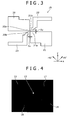
- a design pattern 19 for forming the source electrode 13, the drain electrode 14, and the gate electrodes 17 and 18, like that shown in FIG. 3 is transferred by exposure with use of e.g. variable-shaped electron beam exposure apparatus.
- a pattern 20 corresponding to the source electrode 13 is first transferred for example.
- a pattern 21 corresponding to the drain electrode 14 is so transferred that a vertex 21b of a corner part 21a is disposed at a position distant from a vertex 20b of a corner part 20a of the pattern 20 by ⁇ x along the x-axis direction and ⁇ y along the y-axis direction.
- patterns 22 and 23 corresponding to the gate electrodes 17 and 18 are transferred.
- FIG. 2(A) a resist pattern 24 to which the design pattern 19 is transferred as aperture patterns is formed.
- This resist pattern 24 has aperture patterns with shapes corresponding to the source electrode 13, the drain electrode 14, and the gate electrodes 17 and 18.
- FIG. 2(A) only aperture patterns 24a and 24b with shapes corresponding to the source electrode 13 and the drain electrode 14 are shown.
- part 24c between these aperture patterns 24a and 24b is part to become the gap 15 finally.
- an electrode film 25 is formed over the semiconductor substrate 11 and on the resist pattern 24 by e.g. a vacuum evaporation method.
- the material of the electrode film 25 is arbitrarily selected from conventionally publicly-known electrically-conductive materials. For example, a multilayer film obtained by sequentially stacking a chromium (Cr) film having a thickness of 5 nm and a gold (Au) film having a thickness of 20 nm, a polycrystalline Si film doped with an impurity and having a thickness of e.g. about 50 nm, etc. is used.
- the resist pattern 24 is removed together with the electrode film 25 formed thereon.
- the source electrode 13, the drain electrode 14, and the gate electrodes 17 and 18 are formed at the parts where the aperture patterns 24a and 24b existed and the parts where the aperture patterns with the shapes corresponding to the gate electrodes 17 and 18 existed, respectively.
- the distance of the gap 15 between the source electrode 13 and the drain electrode 14 can be set equal to or shorter than 20 nm for example.
- the gap 15 between the source electrode 13 and the drain electrode 14 is bridged by the functional molecule 16.
- a solution containing this functional molecule 16 is dropped or applied onto an area including at least the gap 15 over the semiconductor substrate 11, or the semiconductor substrate 11 is immersed in the solution containing the functional molecule 16.
- the functional molecule 16 in this solution enters the gap 15 and is connected between the source electrode 13 and the drain electrode 14 by self-assembly.
- the excess functional molecules 16 left on the surface of the semiconductor substrate 11 are removed by cleaning.
- a substance obtained by coupling a thiol group (-SH) to one end and the other end of an oligofluorene main chain of a n-conjugated molecule with a structural liquid crystal side chain, shown in FIG. 7 to be described later is used as the functional molecule 16, e.g. the following way is employed.
- FIG. 4 A scanning electron microscope (SEM) picture of the source electrode 13, the drain electrode 14, and the gate electrodes 17 and 18 actually fabricated by the above-described method is shown in FIG. 4 . From FIG. 4 , it turns out that the distance of the gap 15 between the source electrode 13 and the drain electrode 14 is 11.8 nm, i.e. extremely short.
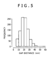
- FIG. 5 shows a frequency distribution graph of the result of measurement of the distances of the gaps 15 finally obtained by transferring the above-described design patterns 19 to the entire surface of the semiconductor substrate 11 (semiconductor wafer) having a diameter of 200 mm by electron beam exposure.
- the source electrode 13 and the drain electrode 14 having e.g. the gap 15 whose distance is equal to or shorter than 20 nm can be formed with a high yield.
- the intended molecular element 10 of the field effect type is manufactured.
- the functional molecule 16 arises from covalent linkage of a side chain composed of a pendant molecule to a main chain composed of a conjugated molecule in which structural change (change in the conformation) occurs due to orientation change of this pendent molecule and an electrical characteristic changes.
- This pendant molecule has dielectric constant anisotropy and/or dipole moments, and orientation change thereof occurs due to an electric field.
- This functional molecule 16 is schematically shown in FIG. 6 .
- this functional molecule 16 has a main chain 31 and a side chain 32 in the form of a line or a film, and the side chain 32 is covalently linked to the main chain 31.
- the main chain 31 has a conjugated system and exhibits electrical conductivity due to delocalized n-electrons.
- the side chain 32 has plural dipole moments and/or dielectric constant anisotropy, and the side chain 32 composed of a pendant molecule in which orientation change occurs due to an electric field has a tendency to be oriented in a specific direction with respect to the orientation of an electric field in the electric field (specifically, such a parallel direction that the longitudinal-axis direction of the molecule corresponds with the orientation of the electric field or a perpendicular direction) because the side chain 32 has dielectric constant anisotropy and/or dipole moments.
- the electric field applied to the side chain 32 is changed to thereby change the position of the side chain 32 with respect to the electric field direction, and as the result thereof, the angle formed by the side chain 32 and the main chain 31 is changed.
- the electrical conductivity (ease of electron flowing) of the main chain 31 can be controlled.
- the dihedral angle (torsion angle) of the main chain 31 composed of the conjugated molecule is close to that of a flat plane. In this state, electrons in the main chain 31 composed of the conjugated molecule can flow without being interrupted and this functional molecule 16 is in the conductive (on) state.
- this functional molecule 16 is in the conductive (on) state.
- conjugated molecule of this functional molecule e.g. the following electrically-conductive oligomers and so forth are cited.
- the conjugated molecule is not limited thereto.
- a molecule having a fluorene skeleton is preferable as the conjugated molecule.
- this conjugated molecule is not limited to them.
- a molecule having a cyanobiphenyl skeleton is preferable as this pendent molecule.
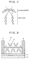
- FIG. 7 shows a specific example of the functional molecule 16.
- This functional molecule 16 is a ⁇ -conjugated molecule with a structural liquid crystal side chain and has an oligofluorene main chain and a liquid crystal side chain composed of 4-pentyl-4'-cyanobiphenyl.
- a thiol group (-SH) is coupled to one end and the other end of the oligofluorene main chain.
- the length of the oligofluorene main chain of this functional molecule 16 differs depending on the degree of polymerization of the oligofluorene. For example, the length is about 7 to 10 nm if the degree of polymerization is 7 to 10.
- FIG. 8 schematically shows the state in which the gap 15 between the source electrode 13 and the drain electrode 14 is bridged by this n-conjugated molecule with the structural liquid crystal side chain.
- one end and the other end of the oligofluorene main chain of this n-conjugated molecule with the structural liquid crystal side chain are coupled to the tip part of the source electrode 13 and the tip part of the drain electrode 14, respectively, via the thiol group.
- the stable structure of the whole of the molecule including the oligofluorene main chain changes due to change in the orientation of the side chain, and the dihedral angle of the oligofluorene main chain changes along with increase in the gate voltage.
- electrical conductivity develops. It is known that the stable dihedral angle of oligofluorene changes if the side chain is different.
- FIG. 10 shows a molecular element according to a second embodiment.
- FIG. 10(A) is a plan view
- FIG. 10(B) is an enlarged sectional view along line X-X in FIG. 10(A) .
- a gate electrode 41 is provided on the insulating film 12, such as a SiO 2 film, formed on the semiconductor substrate 11 and having a thickness of e.g. about 100 nm.
- An insulating film 42 such as a SiO 2 film is so provided as to cover this gate electrode 41.
- the source electrode 13 and the drain electrode 14 are provided on this insulating film 42.
- the functional molecule 16 is provided as a bridge between the vertices 13b and 14b of the corner parts 13a and 14a of these source electrode 13 and drain electrode 14. In this case, an electric field is applied to the functional molecule 16 by voltage (gate voltage) applied to the gate electrode 41, to control this functional molecule 16.
- the gate electrode 41 is formed on the insulating film 12 formed on the semiconductor substrate 11.
- the insulating film 42 is so formed as to cover this gate electrode 41.
- the source electrode 13 and the drain electrode 14 are so formed as to be opposed to each other with the intermediary of the gap 15 by a method similar to that of the first embodiment.
- the gap 15 between the source electrode 13 and the drain electrode 14 is bridged by the functional molecule 16 by a method similar to that of the first embodiment.
- FIG. 11 shows the measurement result of the current-voltage characteristic when the gate electrode 41 is grounded and the bias voltage between the source electrode 13 and the drain electrode 14 is changed at 8 K in the molecular element 10 according to the second embodiment in which the molecule shown in FIG. 7 is used as the functional molecule 16.
- the distance of the gap 15 between the source electrode 13 and the drain electrode 14 is 7.5 nm
- the source electrode 13 and the drain electrode 14 are formed of a gold film having a thickness of 20 nm.
- the insulating film 42 is formed of a SiO 2 film, and the thickness of the SiO 2 film as the insulating film 42 between the gate electrode 41 and the source electrode 13 and the drain electrode 14 is 50 nm. As shown in FIG.
- steps due to the molecular orbital of the functional molecule 16 are observed in the current-voltage curve, and thus it is proven that the number of functional molecules 16 is small enough that the quantum effect is seen.
- the source electrode 13 and the drain electrode 14 are formed from gold, the current-voltage curve is almost symmetrical about positive and negative biases.
- this molecular element 10 can be made to work as a diode by using the anterior and posterior zones of the step.
- FIG. 12 shows the measurement result of the drain current (I ds )-drain voltage (V ds ) characteristic when the gate voltage (voltage applied to the gate electrode 41) is changed at 300 K in the molecular element 10 according to the second embodiment in which the molecule shown in FIG. 7 is used as the functional molecule 16.
- the gate voltage V g and the drain voltage V ds are each voltage on the basis of the ground potential.
- the source electrode 13 was grounded. From FIG. 12 , it turns out that this molecular element 10 exhibits opposite diode characteristics depending on the polarity of the gate voltage V g .
- This molecular element 10 can also be turned on/off by the gate voltage V g .
- it is also possible to drive the molecular element 10 by a low voltage such as V ds 1 V without using the molecular orbital.
- the above-described measurement results apply also to the molecular element 10 according to the first embodiment in which the molecule shown in FIG. 7 is used as the functional molecule 16.
- the extremely-narrow gap 15 whose distance is equal to or shorter than 20 nm or equal to or shorter than 10 nm can be easily formed with high reproducibility between the source electrode 13 and the drain electrode 14. Furthermore, this gap 15 can be easily bridged by the functional molecule 16. Thereby, the molecular element 10 of the field effect type can be obtained at low cost.
- this molecular element 10 can be made to work as a diode of two kinds of directions by the gate voltage V g although it is one element.
- it can be made to work also as a field effect transistor and furthermore can be made to work also as a memory. That is, as long as this molecular element 10 is made, its function can be switched by control of the gate voltage V g and it can be made to work as a diode, a transistor, or a memory. Therefore, the molecular element 10 does not need to be designed and fabricated in accordance with the specifications, and thus logic circuits, memory circuits, etc. can be manufactured at low cost by using this molecular element 10.
- FIG. 14 shows one example of the configuration of an integrated circuit device (hereinafter, referred to as the IC chip) according to a third embodiment.
- an IC chip 50 has a circuit part 51 having the configuration suitable for the functions given to this IC chip 50 and plural pad electrodes 53 connected to this circuit part 51 by interconnects 52.
- the circuit part 51 includes e.g. a logic circuit, a memory cell array, a sense amplifier, a decoder, etc., and is configured by the molecular elements 10 according to the first or second embodiment, other various kinds of elements, interconnects for connection among elements, and so forth.
- the pad electrodes 53 are provided at the peripheral part of the IC chip 50.
- the pad electrode 53 is obtained by stacking a gold (Au) film having a thickness of 100 nm on a titanium (Ti) film having a thickness of 5 nm for example and is formed by a vacuum evaporation method or the like.
- the IC chip 50 is e.g. a device using a semiconductor substrate such as a Si substrate or a GaAs substrate.
- Elements other than the molecular element 10 in the circuit part 51 can be formed on the semiconductor substrate by a conventionally publicly-known semiconductor technology.
- the molecular element 10 included in the circuit part 51 is used as a diode, a transistor, or a memory by application of the gate voltage, depending on the functions given to the circuit part 51.
- the manufacturing method of these molecular elements 10 is similar to that of the first or second embodiment.
- the circuit part 51, the interconnects 52, the pad electrodes 53, and so forth are formed on the semiconductor substrate 11 by using a conventionally publicly-known semiconductor technology.
- the functional molecule 16 has not yet been formed in the gap 15 between the source electrode 13 and the drain electrode 14 of the molecular element 10 included in the circuit part 51.
- the gap 15 between the source electrode 13 and the drain electrode 14 is bridged by the functional molecule 16 by a method similar to that of the first embodiment.
- the semiconductor substrate 11 is turned to chips. In this manner, the IC chip 50 is manufactured.
- the molecular element 10 included in the circuit part 51 can be made to work as a diode, a transistor, or a memory by application of the gate voltage, depending on the functions given to the circuit part 51.
- the circuit part 51 can be inexpensively configured. Consequently, the manufacturing cost of the IC chip 50 can be reduced.
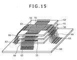
- FIG. 15 explains a three-dimensional integrated circuit device (hereinafter, referred to as the three-dimensional IC) according to a fourth embodiment.
- the IC chip 50 shown in FIG. 14 and one or plural IC chips similar to this IC chip 50 are sequentially stacked over a mounting substrate 60.
- the gap 15 between the source electrode 13 and the drain electrode 14 of the molecular element 10 included in the circuit part 51 of the IC chip 50 is bridged by the functional molecule 16.
- the same also applies to one or plural IC chips similar to this IC chip 50.
- the number of IC chips stacked over the mounting substrate 60 is not particularly limited. Here, the case in which three IC chips 50, 61, and 62 are stacked will be described as one example. These IC chips 50, 61, and 62 may be ones having the same configuration or may be ones different from each other.
- pad electrodes 63 for connection to the pad electrodes 53 of the IC chips 50, 61, and 62 stacked over this mounting substrate 60 are provided.
- a gap 64 of a predetermined distance is set between the mounting substrate 60 and the IC chip 50, between the IC chip 50 and the IC chip 61, and between the IC chip 61 and the IC chip 62.
- spacers 65 having a predetermined thickness are each provided between the mounting substrate 60 and the IC chip 50, between the IC chip 50 and the IC chip 61, and between the IC chip 61 and the IC chip 62.
- this spacer 65 e.g. a glass bead is used.
- the spacer 65 is not limited thereto.
- the distance of the gap 64 is arbitrarily selected, such a size that a solution containing the functional molecule 16 can be injected into this gap 64 by capillary action as described later is selected. Specifically, e.g. about 30 ⁇ m is selected. Bonding is made by wires 66 between the pad electrodes 63 of the mounting substrate 60 and the pad electrodes 53 of the IC chips 50, 61, and 62.
- the IC chip 50, the IC chip 61, and the IC chip 62 are sequentially stacked over the mounting substrate 60, with the spacers 65 sandwiched between the IC chips.
- the functional molecule 16 is not connected to the gap 15 between the source electrode 13 and the drain electrode 14 of the molecular element 10 included in the circuit part 51 of the IC chip 50.
- bonding is made by the wires 66 between the pad electrodes 63 of the mounting substrate 60 and the pad electrodes 53 of the IC chips 50, 61, and 62.
- the component obtained by stacking the IC chips 50, 61, and 62 over the mounting substrate 60 and making the bonding by the wires 66 in this manner is immersed in a solution containing the functional molecule 16. Furthermore, this solution is injected into each of the gaps 64 among the mounting substrate 60 and the IC chips 50, 61, and 62 by capillary action.
- the temperature in the injection of this solution can be arbitrarily selected. For example, the injection is performed at a room temperature.
- the component obtained by stacking the IC chips 50, 61, and 62 over the mounting substrate 60 is taken out from the solution to the air.
- the molecular element 10 of the field effect type in which the functional molecule 16 is connected between the source electrode 13 and the drain electrode 14 is completed and hence the IC chips 50, 61, and 62 are completed.
- a circuit is turned to a three-dimensional one by stacking, over the mounting substrate 60, the IC chips 50, 61, and 62 in which the functional molecule 16 is not formed between the source electrode 13 and the drain electrode 14 of the molecular element 10. Furthermore, thereafter, a solution containing the functional molecule 16 is injected into the gaps 64 among the IC chips 50, 61, and 62 by capillary action, and the gap 64 between the source electrode 13 and the drain electrode 14 is bridged by the functional molecule 16 in this solution by self-assembly. Therefore, a high-temperature process or the like does not need to be carried out after the completion of the molecular element 10, and the deterioration of the functional molecule 16 can be prevented. Consequently, the deterioration of the performance of the molecular element 10 can be prevented.
- the manufacturing steps can be simplified compared with conventional three-dimensional ICs, and hence the manufacturing cost can be reduced.
- FIG. 18 shows a three-dimensional IC according to a fifth embodiment.
- the IC chips 50, 61, and 62 and the mounting substrate 60 are electrically connected to each other by through-interconnects 71 provided in such a manner as to penetrate each of the IC chips and the substrate, differently from the fourth embodiment.
- the pad electrodes 53 are not provided on the IC chips 50, 61, and 62.
- the pad electrodes 63 are not provided on the mounting substrate 60.
- the through-interconnects 71 play a role similar to that of these pad electrodes 53 and 63.
- the through-interconnect 71 can be formed in the following manner for example.
- a via-hole penetrating them is formed in the IC chips 50, 61, and 62 and the mounting substrate 60.
- An insulating film such as a SiO 2 film is formed on the inner wall of this via-hole.
- an electrically-conductive material such as Cu is buried in the inside of this via-hole.
- the through-interconnect 71 is formed.
- the diameter of this via-hole is arbitrarily decided and is e.g. about 100 ⁇ m.
- the characteristics other than the above-described characteristic are the same as those of the fourth embodiment. According to this fifth embodiment, the same advantages as those of the fourth embodiment can be obtained.
- FIG. 19 shows a three-dimensional IC according to a sixth embodiment.
- the IC chips 50, 61, and 62 and the mounting substrate 60 are electrically connected to each other by molecular interconnects 72, differently from the first and second embodiments.
- the molecular interconnect 72 is connected to the through-interconnects 71 provided in such a manner as to penetrate each of the IC chips 50, 61, and 62 and the mounting substrate 60.
- the pad electrodes 53 are not provided on the IC chips 50, 61, and 62.
- the pad electrodes 63 are not provided on the mounting substrate 60.
- the through-interconnects 71 play a role similar to that of these pad electrodes 53 and 63.
- the molecular interconnect 72 a conventionally publicly-known molecular interconnect can be used. It can be formed by a conventionally publicly-known method (refer to e.g. Patent Document 2 and Non-Patent Document 1).
- the molecular interconnect 72 is not particularly limited but e.g. polypyrrole is used.
- polypyrrole a description about a method for forming this molecular interconnect 72 by electropolymerization is as follows. First, similarly to the fifth embodiment, the through-interconnects 71 are formed in the IC chips 50, 61, and 62, and the mounting substrate 60. Next, similarly to the fourth embodiment, the IC chips 50, 61, and 62 are sequentially stacked over the mounting substrate 60.
- an electrically-conductive plate (not shown) is provided on the upper surface of the uppermost IC chip 62 and is brought into electrical contact with the through-interconnects 71.
- an electrolytic solution a pyrrole solution prepared by employing deoxygenated acetonitrile as the solvent is used.
- the concentration is 0.05 to 0.1 mol/ml and the electrolyte concentration is 0.1 to 0.3 mol/ml.
- the electrolyte e.g. LiClO4, LiBF4, Et4NCl4, Et4NBF4, etc. is used.
- a counter electrode is provided in the electrolytic solution.
- This counter electrode is used as a negative electrode and the above-described electrically-conductive plate is used as a positive electrode.
- a voltage of e.g. about 3.5 V is applied between both electrodes and electropolymerization is performed in the electrolytic solution.
- the pyrrole solution which is a monomer solution, in the electrolytic solution is injected into each of the gaps 64 among the mounting substrate 60 and the IC chips 50, 61, and 62 by capillary action.
- polypyrrole is formed by the electropolymerization of pyrrole between the through-interconnects 71 opposed to each other with the intermediary of the gaps 64 of the IC chips 50, 61, and 62 and the mounting substrate 60.
- the molecular interconnect 72 is formed. It is also possible to form an element such as a diode between the through-interconnects 71 by utilizing the behavior that the polypyrrole is generated from the positive electrode side, according to need.
- the characteristics other than the above-described characteristic are the same as those of the fourth embodiment. According to this sixth embodiment, the same advantages as those of the fourth embodiment can be obtained.
Landscapes
- Engineering & Computer Science (AREA)
- Chemical & Material Sciences (AREA)
- Nanotechnology (AREA)
- Physics & Mathematics (AREA)
- Crystallography & Structural Chemistry (AREA)
- Theoretical Computer Science (AREA)
- Mathematical Physics (AREA)
- Spectroscopy & Molecular Physics (AREA)
- Materials Engineering (AREA)
- Thin Film Transistor (AREA)
- Semiconductor Memories (AREA)
- Metal-Oxide And Bipolar Metal-Oxide Semiconductor Integrated Circuits (AREA)
- Electroluminescent Light Sources (AREA)
Abstract

Description
- This invention relates to molecular elements, manufacturing methods thereof, integrated circuit devices, manufacturing methods thereof, three-dimensional integrated circuit devices, and manufacturing methods thereof. More specifically, this invention relates to a molecular element whose function can be switched by electric field control, a manufacturing method thereof, an integrated circuit device using this molecular element, a manufacturing method thereof, a three-dimensional integrated circuit device using this molecular element, and a manufacturing method thereof.
- In the silicon-based semiconductor element, a transistor is designed and fabricated as a transistor and a diode is designed and fabricated as a diode in accordance with the specifications. Therefore, for example, a field effect transistor can not be used as a diode. Furthermore, a field effect transistor also does not have memory performance. Because semiconductor elements need to be designed and fabricated in accordance with the specifications as just described, it is difficult to reduce the manufacturing cost.
- On the other hand, the present assignee has proposed a functional molecule and a functional molecule element having a gate electrode, a source electrode, and a drain electrode (refer to e.g. Patent Document 1). This functional molecule has a side chain composed of a pendant molecule that has dielectric constant anisotropy and/or dipole moments and in which orientation change occurs due to an electric field.
This side chain is covalently linked to a main chain composed of a conjugated molecule in which structural change occurs due to the orientation change of the pendent molecule and an electrical characteristic changes. The source electrode and the drain electrode are connected to one end and the other end, respectively, of this main chain. The gate electrode is to apply an electric field for control to the pendant molecule. -
- Patent Document 1:
Japanese Patent Laid-Open No. 2006- 108627 - Patent Document 2:
Japanese Patent Laid-Open No. 2006- 351623 -
- Non-Patent Document 1: "Doudensei Koubunshi," compiled by Naoya Ogata, issued by Kodansha Scientific Ltd. (1990)
- In
Patent Document 1, it is described that the above-described functional molecule element can be applied to various electronic device fields such as switch, transistor, memory, and logic circuit. However, details thereof are not necessarily clear. - Thus, a problem to be solved by this invention is to provide such a molecular element that one molecular element can be used as a diode, a transistor, or a memory by control of the applied electric field and an element having the necessary functions can be inexpensively obtained, and a manufacturing method thereof.
In other words, a problem to be solved by this invention is to provide such a molecular element that the function of one molecular element can be switched by control of the applied electric field and an element having the necessary functions can be inexpensively obtained, and a manufacturing method thereof.
Another problem to be solved by this invention is to provide an integrated circuit device using the above-described molecular element, a manufacturing method thereof, a three-dimensional integrated circuit device using the above-described molecular element, and a manufacturing method thereof. - To solve the above-described problems, a first invention is
a molecular element having
a functional molecule in which a side chain composed of a pendant molecule that has dielectric constant anisotropy and/or a dipole moment and in which orientation change occurs due to an electric field is covalently linked to a main chain composed of a conjugated molecule in which structural change occurs due to the orientation change of the pendant molecule and an electrical characteristic changes,
a source electrode and a drain electrode that are connected to one end and the other end, respectively, of the main chain of the functional molecule, and
a gate electrode for applying an electric field for control to the pendant molecule, and
working as a diode, a transistor, or a memory by an electric field applied to the pendent molecule. - A second invention is
a manufacturing method of a molecular element for the case of manufacturing a molecular element having a functional molecule in which a side chain composed of a pendant molecule that has dielectric constant anisotropy and/or a dipole moment and in which orientation change occurs due to an electric field is covalently linked to a main chain composed of a conjugated molecule in which structural change occurs due to the orientation change of the pendant molecule and an electrical characteristic changes, a source electrode and a drain electrode that are connected to one end and the other end, respectively, of the main chain of the functional molecule, and a gate electrode for applying an electric field for control to the pendant molecule, and working as a diode, a transistor, or a memory by an electric field applied to the pendent molecule. The manufacturing method has
a step of forming the source electrode and the drain electrode over a substrate,
a step of bridging a gap between the source electrode and the drain electrode by the functional molecule in such a manner that the source electrode and the drain electrode are connected to one end and the other end, respectively, of the main chain, and
a step of forming the gate electrode over the substrate. - A third invention is
an integrated circuit device having at least one molecular element having a functional molecule in which a side chain composed of a pendant molecule that has dielectric constant anisotropy and/or a dipole moment and in which orientation change occurs due to an electric field is covalently linked to a main chain composed of a conjugated molecule in which structural change occurs due to the orientation change of the pendant molecule and an electrical characteristic changes, a source electrode and a drain electrode that are connected to one end and the other end, respectively, of the main chain of the functional molecule, and a gate electrode for applying an electric field for control to the pendant molecule, and working as a diode, a transistor, or a memory by an electric field applied to the pendent molecule. - A fourth invention is
a manufacturing method of an integrated circuit device for the case of manufacturing an integrated circuit device having at least one molecular element having a functional molecule in which a side chain composed of a pendant molecule that has dielectric constant anisotropy and/or a dipole moment and in which orientation change occurs due to an electric field is covalently linked to a main chain composed of a conjugated molecule in which structural change occurs due to the orientation change of the pendant molecule and an electrical characteristic changes, a source electrode and a drain electrode that are connected to one end and the other end, respectively, of the main chain of the functional molecule, and a gate electrode for applying an electric field for control to the pendant molecule, and working as a diode, a transistor, or a memory by an electric field applied to the pendent molecule. The manufacturing method has
a step of forming the source electrode and the drain electrode over a substrate,
a step of bridging a gap between the source electrode and the drain electrode by the functional molecule in such a manner that the source electrode and the drain electrode are connected to one end and the other end, respectively, of the main chain, and
a step of forming the gate electrode over the substrate. - A fifth invention is
a three-dimensional integrated circuit device obtained by disposing a plurality of substrates that are opposed to each other and include at least one substrate having at least one molecular element having a functional molecule in which a side chain composed of a pendant molecule that has dielectric constant anisotropy and/or a dipole moment and in which orientation change occurs due to an electric field is covalently linked to a main chain composed of a conjugated molecule in which structural change occurs due to the orientation change of the pendant molecule and an electrical characteristic changes, a source electrode and a drain electrode that are connected to one end and the other end, respectively, of the main chain of the functional molecule, and a gate electrode for applying an electric field for control to the pendant molecule, and working as a diode, a transistor, or a memory by an electric field applied to the pendent molecule. - A sixth invention is
a manufacturing method of a three-dimensional integrated circuit device for the case of manufacturing a three-dimensional integrated circuit device obtained by disposing a plurality of substrates that are opposed to each other and include at least one substrate having at least one molecular element having a functional molecule in which a side chain composed of a pendant molecule that has dielectric constant anisotropy and/or a dipole moment and in which orientation change occurs due to an electric field is covalently linked to a main chain composed of a conjugated molecule in which structural change occurs due to the orientation change of the pendant molecule and an electrical characteristic changes, a source electrode and a drain electrode that are connected to one end and the other end, respectively, of the main chain of the functional molecule, and a gate electrode for applying an electric field for control to the pendant molecule, and working as a diode, a transistor, or a memory by an electric field applied to the pendent molecule. The manufacturing method has
a step of forming the source electrode and the drain electrode over the at least one substrate,
a step of bridging a gap between the source electrode and the drain electrode by the functional molecule in such a manner that the source electrode and the drain electrode are connected to one end and the other end, respectively, of the main chain, and
a step of forming the gate electrode over the at least one substrate. - In this invention configured as described above, by only properly selecting the electric field applied to the pendant molecule of the functional molecule by the gate electrode, the molecular element can be made to work as a diode, a transistor, or a memory. Therefore, the molecular element does not need to be designed and fabricated in accordance with the specifications.
- According to this invention, one molecular element can be used as a diode, a transistor, or a memory by control of the applied electric field. In other words, such a molecular element that the function can be switched and an element having the necessary functions can be inexpensively obtained can be realized. Furthermore, high-performance integrated circuit device and three-dimensional integrated circuit device can be inexpensively realized by using this molecular element.
-
- [
FIG. 1 ]
FIG. 1 is a plan view and a sectional view showing a molecular element according to a first embodiment of this invention. - [
FIG. 2 ]
FIG. 2 is a sectional view for explaining a manufacturing method of the molecular element according to the first embodiment of this invention. - [
FIG. 3 ]
FIG. 3 is a plan view showing a design pattern used when a source electrode, a drain electrode, and gate electrodes are formed by electron beam exposure in the manufacturing method of the molecular element according to the first embodiment of this invention. - [
FIG. 4 ]
FIG. 4 is a diagram-substitute picture showing the result of forming of the source electrode, the drain electrode, and the gate electrodes by electron beam exposure with use of the design pattern shown inFIG. 3 . - [
FIG. 5 ]
FIG. 5 is a schematic diagram showing the frequency distribution of the distance of the gap between the source electrode and the drain electrode when the source electrode, the drain electrode, and the gate electrodes are formed by electron beam exposure with use of the design pattern shown inFIG. 3 . - [
FIG. 6 ]
FIG. 6 is a schematic diagram showing one example of a functional molecule formed in the gap between the source electrode and the drain electrode in the molecular element according to the first embodiment of this invention. - [
FIG. 7 ]
FIG. 7 is a schematic diagram showing a specific example of the functional molecule shown inFIG. 6 . - [
FIG. 8 ]
FIG. 8 is a sectional view showing the state in which the functional molecule shown inFIG. 7 is formed in the gap between the source electrode and the drain electrode in the molecular element according to the first embodiment of this invention. - [
FIG. 9 ]
FIG. 9 is a schematic diagram for explaining the mechanism of control of the electrical conductivity of the functional molecule shown inFIG. 7 by electric field application. - [
FIG. 10 ]
FIG. 10 is a plan view and a sectional view showing a molecular element according to a second embodiment of this invention. - [
FIG. 11 ]
FIG. 11 is a schematic diagram showing the measurement result of the current-voltage characteristic of the molecular element according to the second embodiment of this invention. - [
FIG. 12 ]
FIG. 12 is a schematic diagram showing the measurement result of the drain current-drain voltage characteristic when the gate voltage is changed in the molecular element according to the second embodiment of this invention. - [
FIG. 13 ]
FIG. 13 is a schematic diagram showing the measurement result of the drain current when the gate voltage is changed in the molecular element according to the second embodiment of this invention. - [
FIG. 14 ]
FIG. 14 is a perspective view showing an integrated circuit device according to a third embodiment of this invention. - [
FIG. 15 ]
FIG. 15 is a perspective view showing a three-dimensional integrated circuit device according to a fourth embodiment of this invention. - [
FIG. 16 ]
FIG. 16 is a sectional view ofFIG. 15 . - [
FIG. 17 ]
FIG. 17 is a perspective view for explaining a manufacturing method of the three-dimensional integrated circuit device according to the fourth embodiment of this invention. - [
FIG. 18 ]
FIG. 18 is a perspective view showing a three-dimensional integrated circuit device according to a fifth embodiment of this invention. - [
FIG. 19 ]
FIG. 19 is a sectional view showing a three-dimensional integrated circuit device according to a sixth embodiment of this invention. - Best modes for carrying out the invention (hereinafter, referred to as the embodiments) will be described below.
The description will be made in the following order. -
FIG. 1 shows one example of the configuration of a molecular element according to a first embodiment. Here,FIG. 1(A) is a plan view andFIG. 1(B) is an enlarged sectional view along line X-X inFIG. 1(A) .
As shown inFIG. 1(A) and FIG. 1(B) , in thismolecular element 10, asource electrode 13 and adrain electrode 14 are provided on an insulatingfilm 12 formed on asemiconductor substrate 11. Thesemiconductor substrate 11 is e.g. a Si substrate, a GaAs substrate, or the like. The insulatingfilm 12 is e.g. a SiO2 film or the like having a thickness of about 100 nm. - The
source electrode 13 and thedrain electrode 14 havecorner parts Vertices corner parts gap 15 and are opposed to each other. Thegap 15 between thesevertices functional molecule 16. Thefunctional molecule 16 will be described in detail later. These source electrode 13 anddrain electrode 14 can be formed from various kinds of conventionally publicly-known metal films (films composed of an elemental metal, films composed of an alloy, etc.), semiconductor films doped with an impurity, etc. - The distance between the
vertices source electrode 13 and thedrain electrode 14, in other words, the distance of thegap 15, is arbitrarily decided depending on the length of thefunctional molecule 16. The distance is generally equal to or shorter than 20 nm and typically equal to or shorter than 10 nm.
On the insulatingfilm 12, a pair ofgate electrodes functional molecule 16 connected between thevertices source electrode 13 and thedrain electrode 14. An electric field is applied to thefunctional molecule 16 by voltage (gate voltage) applied between thesegate electrodes functional molecule 16. Thesegate electrodes source electrode 13, thedrain electrode 14, and thegate electrodes
As described in detail later, thismolecular element 10 can be used as a diode, a transistor, or a memory, and in addition as a resistor, according to need. - A manufacturing method of the
molecular element 10 will be described.
First, as shown inFIG. 2(A) , a positive resist (e.g. chemically-amplified positive resist for electron beam exposure, OEBR-CAP138 PM, made by TOKYO OHKA KOGYO CO., LTD.) is applied on the insulatingfilm 12 formed on thesemiconductor substrate 11, so that a resist film (not shown) is formed. - Next, to this resist film, a
design pattern 19 for forming thesource electrode 13, thedrain electrode 14, and thegate electrodes FIG. 3 , is transferred by exposure with use of e.g. variable-shaped electron beam exposure apparatus. Specifically, as shown inFIG. 3 , apattern 20 corresponding to thesource electrode 13 is first transferred for example. Next, apattern 21 corresponding to thedrain electrode 14 is so transferred that avertex 21b of acorner part 21a is disposed at a position distant from avertex 20b of acorner part 20a of thepattern 20 by Δx along the x-axis direction and Δy along the y-axis direction. Δx and Δy are arbitrarily selected. To cite a case, Δx = Δy = 30 nm. Next,patterns gate electrodes - Next, the resist film for which exposure has been performed in the above-described manner is developed. Thereby, as shown in
FIG. 2(A) , a resistpattern 24 to which thedesign pattern 19 is transferred as aperture patterns is formed. This resistpattern 24 has aperture patterns with shapes corresponding to thesource electrode 13, thedrain electrode 14, and thegate electrodes FIG. 2(A) ,only aperture patterns source electrode 13 and thedrain electrode 14 are shown. Of the resistpattern 24,part 24c between theseaperture patterns gap 15 finally. - In the above-described manner, transferring is so performed by electron beam exposure that the
pattern 20 corresponding to thesource electrode 13 and thepattern 21 corresponding to thedrain electrode 14 are disposed in such a state that theirvertices vertices patterns pattern 24, thepart 24c between theaperture patterns gap 15 finally, can be formed with a minute width. - Next, as shown in
FIG. 2(B) , anelectrode film 25 is formed over thesemiconductor substrate 11 and on the resistpattern 24 by e.g. a vacuum evaporation method. The material of theelectrode film 25 is arbitrarily selected from conventionally publicly-known electrically-conductive materials. For example, a multilayer film obtained by sequentially stacking a chromium (Cr) film having a thickness of 5 nm and a gold (Au) film having a thickness of 20 nm, a polycrystalline Si film doped with an impurity and having a thickness of e.g. about 50 nm, etc. is used. - Next, by a lift-off method, the resist
pattern 24 is removed together with theelectrode film 25 formed thereon. Thereby, as shown inFIG. 2(C) , thesource electrode 13, thedrain electrode 14, and thegate electrodes aperture patterns gate electrodes gap 15 between thesource electrode 13 and thedrain electrode 14 can be set equal to or shorter than 20 nm for example. - Next, as shown in
FIG. 2(D) , thegap 15 between thesource electrode 13 and thedrain electrode 14 is bridged by thefunctional molecule 16. To bridge thegap 15 by thefunctional molecule 16, for example, a solution containing thisfunctional molecule 16 is dropped or applied onto an area including at least thegap 15 over thesemiconductor substrate 11, or thesemiconductor substrate 11 is immersed in the solution containing thefunctional molecule 16. By doing so, thefunctional molecule 16 in this solution enters thegap 15 and is connected between thesource electrode 13 and thedrain electrode 14 by self-assembly. - After the solution containing the
functional molecule 16 is dropped or applied over thesemiconductor substrate 11 or thesemiconductor substrate 11 is immersed in this solution, the excessfunctional molecules 16 left on the surface of thesemiconductor substrate 11 are removed by cleaning.
Concretely, for example if a substance obtained by coupling a thiol group (-SH) to one end and the other end of an oligofluorene main chain of a n-conjugated molecule with a structural liquid crystal side chain, shown inFIG. 7 to be described later, is used as thefunctional molecule 16, e.g. the following way is employed. Specifically, 1 µL of a 1-mmol/L tetrahydrofuran (THF) solution of this molecule is dropped onto an area including thegap 15, thesource electrode 13, and thedrain electrode 14, and is kept stationary under the THF-saturated vapor pressure for 24 hours. Thereafter, the excess molecules are removed by cleaning with THF.
By the above-described process, the intendedmolecular element 10 of the field effect type is manufactured. - A scanning electron microscope (SEM) picture of the
source electrode 13, thedrain electrode 14, and thegate electrodes FIG. 4 . FromFIG. 4 , it turns out that the distance of thegap 15 between thesource electrode 13 and thedrain electrode 14 is 11.8 nm, i.e. extremely short. -
FIG. 5 shows a frequency distribution graph of the result of measurement of the distances of thegaps 15 finally obtained by transferring the above-describeddesign patterns 19 to the entire surface of the semiconductor substrate 11 (semiconductor wafer) having a diameter of 200 mm by electron beam exposure. As shown inFIG. 5 , it was confirmed that a sufficient number of electrode patterns were obtained with a peak around 20 nm = the distance of thegap 15. The percentage of distances equal to or shorter than 20 nm, of the obtainedgaps 15, was about 30%. - As described above, by transferring the
design pattern 19 shown inFIG. 3 to a resist film by electron beam exposure, thesource electrode 13 and thedrain electrode 14 having e.g. thegap 15 whose distance is equal to or shorter than 20 nm can be formed with a high yield.
By the above-described process, the intendedmolecular element 10 of the field effect type is manufactured. - The
functional molecule 16 arises from covalent linkage of a side chain composed of a pendant molecule to a main chain composed of a conjugated molecule in which structural change (change in the conformation) occurs due to orientation change of this pendent molecule and an electrical characteristic changes. This pendant molecule has dielectric constant anisotropy and/or dipole moments, and orientation change thereof occurs due to an electric field. - This
functional molecule 16 is schematically shown inFIG. 6 . As shown inFIGS. 6(A) and (B) , thisfunctional molecule 16 has amain chain 31 and aside chain 32 in the form of a line or a film, and theside chain 32 is covalently linked to themain chain 31. Themain chain 31 has a conjugated system and exhibits electrical conductivity due to delocalized n-electrons. Theside chain 32 has plural dipole moments and/or dielectric constant anisotropy, and theside chain 32 composed of a pendant molecule in which orientation change occurs due to an electric field has a tendency to be oriented in a specific direction with respect to the orientation of an electric field in the electric field (specifically, such a parallel direction that the longitudinal-axis direction of the molecule corresponds with the orientation of the electric field or a perpendicular direction) because theside chain 32 has dielectric constant anisotropy and/or dipole moments. - Therefore, the electric field applied to the
side chain 32 is changed to thereby change the position of theside chain 32 with respect to the electric field direction, and as the result thereof, the angle formed by theside chain 32 and themain chain 31 is changed. In this manner, the electrical conductivity (ease of electron flowing) of themain chain 31 can be controlled.
In the state shown inFIG. 6(A) , the dihedral angle (torsion angle) of themain chain 31 composed of the conjugated molecule is close to that of a flat plane. In this state, electrons in themain chain 31 composed of the conjugated molecule can flow without being interrupted and thisfunctional molecule 16 is in the conductive (on) state.
In contrast, in the state shown inFIG. 6(B) , because the orientation of theside chain 32 has changed, the dihedral angle of themain chain 31 greatly changes compared with that of a flat plane and the planarity of themain chain 31 is lost. In this state, electrons in themain chain 31 composed of the conjugated molecule are blocked by the torsion of themain chain 31 and can not flow and thisfunctional molecule 16 is in the non-conductive (off) state. - As the conjugated molecule of this
functional molecule 16, e.g. the following electrically-conductive oligomers and so forth are cited. However, the conjugated molecule is not limited thereto. - · oligofluorene
- · oligopyridine
- · porphyrin one-dimensional oligomer
- · oligophenylenevinylene
- · oligo(p-phenylene)
- · oligonaphthalene
- · oligoanthracene
- · oligopyrene
- · oligoazulene
- · oligofuran
- · oligothiophene
- · oligoselenophene
- · oligo(p-phenylene sulfide)
- · oligo(p-phenylene oxide)
- · oligoaniline
- Among them, a molecule having a fluorene skeleton is preferable as the conjugated molecule. Furthermore, as the pendant molecule, e.g. 4-pentyl-4'-cyanobiphenyl, molecules that have a carbonyl group (C=O), a halogen (-Cl or the like), a =N-H group, a -OH group, a =C=S group, etc. having a dipole moment, and so forth are cited. However, this conjugated molecule is not limited to them. Among them, a molecule having a cyanobiphenyl skeleton is preferable as this pendent molecule.
-
FIG. 7 shows a specific example of thefunctional molecule 16. Thisfunctional molecule 16 is a π-conjugated molecule with a structural liquid crystal side chain and has an oligofluorene main chain and a liquid crystal side chain composed of 4-pentyl-4'-cyanobiphenyl. A thiol group (-SH) is coupled to one end and the other end of the oligofluorene main chain. The length of the oligofluorene main chain of thisfunctional molecule 16 differs depending on the degree of polymerization of the oligofluorene. For example, the length is about 7 to 10 nm if the degree of polymerization is 7 to 10. -
FIG. 8 schematically shows the state in which thegap 15 between thesource electrode 13 and thedrain electrode 14 is bridged by this n-conjugated molecule with the structural liquid crystal side chain. As shown inFIG. 8 , one end and the other end of the oligofluorene main chain of this n-conjugated molecule with the structural liquid crystal side chain are coupled to the tip part of thesource electrode 13 and the tip part of thedrain electrode 14, respectively, via the thiol group. - The mechanism of the occurrence of modulation of the electrical conductivity due to electric field application in the above-described n-conjugated molecule with the structural liquid crystal side chain will be described based on
FIG. 9 . As shown inFIG. 9(A) to FIG. 9(C) , before electric field application, i.e. when the gate voltage = 0 V, the oligofluorene main chain has a gently-twisted helical structure in such a state as to be stabilized due to packing between the side chains. - When an electric field is applied, i.e. when the gate voltage is applied, the stable structure of the whole of the molecule including the oligofluorene main chain changes due to change in the orientation of the side chain, and the dihedral angle of the oligofluorene main chain changes along with increase in the gate voltage. As a result, electrical conductivity develops. It is known that the stable dihedral angle of oligofluorene changes if the side chain is different.
-
FIG. 10 shows a molecular element according to a second embodiment. Here,FIG. 10(A) is a plan view andFIG. 10(B) is an enlarged sectional view along line X-X inFIG. 10(A) .
As shown inFIG. 10 , in thismolecular element 10, agate electrode 41 is provided on the insulatingfilm 12, such as a SiO2 film, formed on thesemiconductor substrate 11 and having a thickness of e.g. about 100 nm. An insulatingfilm 42 such as a SiO2 film is so provided as to cover thisgate electrode 41. - The
source electrode 13 and thedrain electrode 14 are provided on this insulatingfilm 42. Thefunctional molecule 16 is provided as a bridge between thevertices corner parts source electrode 13 anddrain electrode 14. In this case, an electric field is applied to thefunctional molecule 16 by voltage (gate voltage) applied to thegate electrode 41, to control thisfunctional molecule 16. - As shown in
FIG. 10 , first, thegate electrode 41 is formed on the insulatingfilm 12 formed on thesemiconductor substrate 11. Next, e.g. the insulatingfilm 42 is so formed as to cover thisgate electrode 41. Next, on this insulatingfilm 42, thesource electrode 13 and thedrain electrode 14 are so formed as to be opposed to each other with the intermediary of thegap 15 by a method similar to that of the first embodiment. Thereafter, thegap 15 between thesource electrode 13 and thedrain electrode 14 is bridged by thefunctional molecule 16 by a method similar to that of the first embodiment.
By the above-described process, the intendedmolecular element 10 of the field effect type is manufactured. -
FIG. 11 shows the measurement result of the current-voltage characteristic when thegate electrode 41 is grounded and the bias voltage between thesource electrode 13 and thedrain electrode 14 is changed at 8 K in themolecular element 10 according to the second embodiment in which the molecule shown inFIG. 7 is used as thefunctional molecule 16. The distance of thegap 15 between thesource electrode 13 and thedrain electrode 14 is 7.5 nm, and thesource electrode 13 and thedrain electrode 14 are formed of a gold film having a thickness of 20 nm. Furthermore, the insulatingfilm 42 is formed of a SiO2 film, and the thickness of the SiO2 film as the insulatingfilm 42 between thegate electrode 41 and thesource electrode 13 and thedrain electrode 14 is 50 nm. As shown inFIG. 11 , steps (given voltage values) due to the molecular orbital of thefunctional molecule 16 are observed in the current-voltage curve, and thus it is proven that the number offunctional molecules 16 is small enough that the quantum effect is seen. In this case, because thesource electrode 13 and thedrain electrode 14 are formed from gold, the current-voltage curve is almost symmetrical about positive and negative biases. However, thismolecular element 10 can be made to work as a diode by using the anterior and posterior zones of the step. -
FIG. 12 shows the measurement result of the drain current (Ids)-drain voltage (Vds) characteristic when the gate voltage (voltage applied to the gate electrode 41) is changed at 300 K in themolecular element 10 according to the second embodiment in which the molecule shown inFIG. 7 is used as thefunctional molecule 16. The gate voltage Vg and the drain voltage Vds are each voltage on the basis of the ground potential. Thesource electrode 13 was grounded. FromFIG. 12 , it turns out that thismolecular element 10 exhibits opposite diode characteristics depending on the polarity of the gate voltage Vg. Thismolecular element 10 can also be turned on/off by the gate voltage Vg. Furthermore, it is also possible to drive themolecular element 10 by a low voltage such as Vds = 1 V without using the molecular orbital. - If a higher gate voltage Vg is applied in this
molecular element 10, the molecular structure of thefunctional molecule 16 changes. In addition, with this structure, memory performance that will be attributed to a rotational barrier of the dihedral angle of the fluorene unit develops. How the memory performance develops is shown inFIG. 13 .
As shown inFIG. 13 , when sweeping of the gate voltage Vg from 0 V to - 40 V is repeated three times, Ids suddenly decreases at Vg = - 15 V in the first round of the sweeping (this decrease will be attributed to the occurrence of change in the molecular structure of the functional molecule 16). Since then, Ids is almost constant, and this value of Ids is maintained in the second round and third round of the sweeping. - By utilizing this, this
molecular element 10 can be made to work as a memory. Specifically, if e.g. Vg = - 15 V is employed as the threshold voltage and e.g. data "1" is written to themolecular element 10, the gate voltage Vg lower than this threshold voltage, e.g. 10 V, is applied. Furthermore, in the case of writing data "0", the gate voltage Vg higher than this threshold voltage, e.g. 20 V, is applied.
The above-described measurement results apply also to themolecular element 10 according to the first embodiment in which the molecule shown inFIG. 7 is used as thefunctional molecule 16. - As described above, according to the first and second embodiments, e.g. the extremely-
narrow gap 15 whose distance is equal to or shorter than 20 nm or equal to or shorter than 10 nm can be easily formed with high reproducibility between thesource electrode 13 and thedrain electrode 14. Furthermore, thisgap 15 can be easily bridged by thefunctional molecule 16. Thereby, themolecular element 10 of the field effect type can be obtained at low cost. - Furthermore, this
molecular element 10 can be made to work as a diode of two kinds of directions by the gate voltage Vg although it is one element. In addition, it can be made to work also as a field effect transistor and furthermore can be made to work also as a memory. That is, as long as thismolecular element 10 is made, its function can be switched by control of the gate voltage Vg and it can be made to work as a diode, a transistor, or a memory. Therefore, themolecular element 10 does not need to be designed and fabricated in accordance with the specifications, and thus logic circuits, memory circuits, etc. can be manufactured at low cost by using thismolecular element 10. -
FIG. 14 shows one example of the configuration of an integrated circuit device (hereinafter, referred to as the IC chip) according to a third embodiment.
As shown inFIG. 14 , anIC chip 50 has acircuit part 51 having the configuration suitable for the functions given to thisIC chip 50 andplural pad electrodes 53 connected to thiscircuit part 51 byinterconnects 52. Thecircuit part 51 includes e.g. a logic circuit, a memory cell array, a sense amplifier, a decoder, etc., and is configured by themolecular elements 10 according to the first or second embodiment, other various kinds of elements, interconnects for connection among elements, and so forth. - The
pad electrodes 53 are provided at the peripheral part of theIC chip 50. Thepad electrode 53 is obtained by stacking a gold (Au) film having a thickness of 100 nm on a titanium (Ti) film having a thickness of 5 nm for example and is formed by a vacuum evaporation method or the like. TheIC chip 50 is e.g. a device using a semiconductor substrate such as a Si substrate or a GaAs substrate. - Elements other than the
molecular element 10 in thecircuit part 51, particularly semiconductor elements, can be formed on the semiconductor substrate by a conventionally publicly-known semiconductor technology.
Themolecular element 10 included in thecircuit part 51 is used as a diode, a transistor, or a memory by application of the gate voltage, depending on the functions given to thecircuit part 51. The manufacturing method of thesemolecular elements 10 is similar to that of the first or second embodiment. - The
circuit part 51, theinterconnects 52, thepad electrodes 53, and so forth are formed on thesemiconductor substrate 11 by using a conventionally publicly-known semiconductor technology. At this timing, thefunctional molecule 16 has not yet been formed in thegap 15 between thesource electrode 13 and thedrain electrode 14 of themolecular element 10 included in thecircuit part 51. Next, thegap 15 between thesource electrode 13 and thedrain electrode 14 is bridged by thefunctional molecule 16 by a method similar to that of the first embodiment.
Next, thesemiconductor substrate 11 is turned to chips. In this manner, theIC chip 50 is manufactured. - According to this third embodiment, the
molecular element 10 included in thecircuit part 51 can be made to work as a diode, a transistor, or a memory by application of the gate voltage, depending on the functions given to thecircuit part 51. Thus, thecircuit part 51 can be inexpensively configured. Consequently, the manufacturing cost of theIC chip 50 can be reduced. -
FIG. 15 explains a three-dimensional integrated circuit device (hereinafter, referred to as the three-dimensional IC) according to a fourth embodiment.
As shown inFIG. 15 , in this three-dimensional IC, theIC chip 50 shown inFIG. 14 and one or plural IC chips similar to thisIC chip 50 are sequentially stacked over a mountingsubstrate 60. Thegap 15 between thesource electrode 13 and thedrain electrode 14 of themolecular element 10 included in thecircuit part 51 of theIC chip 50 is bridged by thefunctional molecule 16. The same also applies to one or plural IC chips similar to thisIC chip 50. - The number of IC chips stacked over the mounting
substrate 60 is not particularly limited. Here, the case in which threeIC chips
At the peripheral part of the mountingsubstrate 60,pad electrodes 63 for connection to thepad electrodes 53 of the IC chips 50, 61, and 62 stacked over this mountingsubstrate 60 are provided. - As shown in
FIG. 16 , agap 64 of a predetermined distance is set between the mountingsubstrate 60 and theIC chip 50, between theIC chip 50 and theIC chip 61, and between theIC chip 61 and theIC chip 62. For this purpose, spacers 65 having a predetermined thickness are each provided between the mountingsubstrate 60 and theIC chip 50, between theIC chip 50 and theIC chip 61, and between theIC chip 61 and theIC chip 62. As thisspacer 65, e.g. a glass bead is used. However, thespacer 65 is not limited thereto. Although the distance of thegap 64 is arbitrarily selected, such a size that a solution containing thefunctional molecule 16 can be injected into thisgap 64 by capillary action as described later is selected. Specifically, e.g. about 30 µm is selected.
Bonding is made bywires 66 between thepad electrodes 63 of the mountingsubstrate 60 and thepad electrodes 53 of the IC chips 50, 61, and 62. - A manufacturing method of this three-dimensional IC will be described.
As shown inFIG. 17 , theIC chip 50, theIC chip 61, and theIC chip 62 are sequentially stacked over the mountingsubstrate 60, with thespacers 65 sandwiched between the IC chips. At this timing, thefunctional molecule 16 is not connected to thegap 15 between thesource electrode 13 and thedrain electrode 14 of themolecular element 10 included in thecircuit part 51 of theIC chip 50.
Next, bonding is made by thewires 66 between thepad electrodes 63 of the mountingsubstrate 60 and thepad electrodes 53 of the IC chips 50, 61, and 62. - Next, the component obtained by stacking the IC chips 50, 61, and 62 over the mounting
substrate 60 and making the bonding by thewires 66 in this manner is immersed in a solution containing thefunctional molecule 16. Furthermore, this solution is injected into each of thegaps 64 among the mountingsubstrate 60 and the IC chips 50, 61, and 62 by capillary action. The temperature in the injection of this solution can be arbitrarily selected. For example, the injection is performed at a room temperature. When the solution is thus injected into thegap 64, thegap 15 between thesource electrode 13 and thedrain electrode 14 is bridged by thefunctional molecule 16 in this solution by self-assembly similarly to the first embodiment. Thereafter, the component obtained by stacking the IC chips 50, 61, and 62 over the mountingsubstrate 60 is taken out from the solution to the air. In this manner, themolecular element 10 of the field effect type in which thefunctional molecule 16 is connected between thesource electrode 13 and thedrain electrode 14 is completed and hence the IC chips 50, 61, and 62 are completed.
By the above-described process, the intended three-dimensional IC is manufactured. - As described above, according to this fourth embodiment, a circuit is turned to a three-dimensional one by stacking, over the mounting
substrate 60, the IC chips 50, 61, and 62 in which thefunctional molecule 16 is not formed between thesource electrode 13 and thedrain electrode 14 of themolecular element 10. Furthermore, thereafter, a solution containing thefunctional molecule 16 is injected into thegaps 64 among the IC chips 50, 61, and 62 by capillary action, and thegap 64 between thesource electrode 13 and thedrain electrode 14 is bridged by thefunctional molecule 16 in this solution by self-assembly. Therefore, a high-temperature process or the like does not need to be carried out after the completion of themolecular element 10, and the deterioration of thefunctional molecule 16 can be prevented. Consequently, the deterioration of the performance of themolecular element 10 can be prevented. - Furthermore, by only injecting the solution containing the
functional molecule 16 into thegaps 64 among the IC chips 50, 61, and 62 by capillary action, thegap 15 between thesource electrode 13 and thedrain electrode 14 can be bridged by thefunctional molecule 16. Thus, the manufacturing steps can be simplified compared with conventional three-dimensional ICs, and hence the manufacturing cost can be reduced. -
FIG. 18 shows a three-dimensional IC according to a fifth embodiment.
As shown inFIG. 18 , in this fifth embodiment, the IC chips 50, 61, and 62 and the mountingsubstrate 60 are electrically connected to each other by through-interconnects 71 provided in such a manner as to penetrate each of the IC chips and the substrate, differently from the fourth embodiment. In this case, thepad electrodes 53 are not provided on the IC chips 50, 61, and 62. Similarly, thepad electrodes 63 are not provided on the mountingsubstrate 60. The through-interconnects 71 play a role similar to that of thesepad electrodes - Concretely, the through-
interconnect 71 can be formed in the following manner for example. In the IC chips 50, 61, and 62 and the mountingsubstrate 60, a via-hole penetrating them is formed. An insulating film such as a SiO2 film is formed on the inner wall of this via-hole. Next, an electrically-conductive material such as Cu is buried in the inside of this via-hole. In this manner, the through-interconnect 71 is formed. The diameter of this via-hole is arbitrarily decided and is e.g. about 100 µm.
In this fifth embodiment, the characteristics other than the above-described characteristic are the same as those of the fourth embodiment.
According to this fifth embodiment, the same advantages as those of the fourth embodiment can be obtained. -
FIG. 19 shows a three-dimensional IC according to a sixth embodiment.
As shown inFIG. 19 , in this sixth embodiment, the IC chips 50, 61, and 62 and the mountingsubstrate 60 are electrically connected to each other bymolecular interconnects 72, differently from the first and second embodiments. Themolecular interconnect 72 is connected to the through-interconnects 71 provided in such a manner as to penetrate each of the IC chips 50, 61, and 62 and the mountingsubstrate 60. In this case, thepad electrodes 53 are not provided on the IC chips 50, 61, and 62. Similarly, thepad electrodes 63 are not provided on the mountingsubstrate 60. The through-interconnects 71 play a role similar to that of thesepad electrodes - As the
molecular interconnect 72, a conventionally publicly-known molecular interconnect can be used. It can be formed by a conventionally publicly-known method (refer toe.g. Patent Document 2 and Non-Patent Document 1). Themolecular interconnect 72 is not particularly limited but e.g. polypyrrole is used. Regarding the case of using polypyrrole as themolecular interconnect 72, a description about a method for forming thismolecular interconnect 72 by electropolymerization is as follows.
First, similarly to the fifth embodiment, the through-interconnects 71 are formed in the IC chips 50, 61, and 62, and the mountingsubstrate 60.
Next, similarly to the fourth embodiment, the IC chips 50, 61, and 62 are sequentially stacked over the mountingsubstrate 60. - Next, an electrically-conductive plate (not shown) is provided on the upper surface of the
uppermost IC chip 62 and is brought into electrical contact with the through-interconnects 71.
Next, the whole of the mountingsubstrate 60, the IC chips 50, 61, and 62 and the above-described electrically-conductive plate is immersed in an electrolytic solution. As the electrolytic solution, a pyrrole solution prepared by employing deoxygenated acetonitrile as the solvent is used. In this pyrrole solution, for example, the concentration is 0.05 to 0.1 mol/ml and the electrolyte concentration is 0.1 to 0.3 mol/ml. As the electrolyte, e.g. LiClO4, LiBF4, Et4NCl4, Et4NBF4, etc. is used. - A counter electrode is provided in the electrolytic solution. This counter electrode is used as a negative electrode and the above-described electrically-conductive plate is used as a positive electrode. A voltage of e.g. about 3.5 V is applied between both electrodes and electropolymerization is performed in the electrolytic solution. In this case, the pyrrole solution, which is a monomer solution, in the electrolytic solution is injected into each of the
gaps 64 among the mountingsubstrate 60 and the IC chips 50, 61, and 62 by capillary action. Thereby, polypyrrole is formed by the electropolymerization of pyrrole between the through-interconnects 71 opposed to each other with the intermediary of thegaps 64 of the IC chips 50, 61, and 62 and the mountingsubstrate 60. - In this manner, the
molecular interconnect 72 is formed. It is also possible to form an element such as a diode between the through-interconnects 71 by utilizing the behavior that the polypyrrole is generated from the positive electrode side, according to need.
In this sixth embodiment, the characteristics other than the above-described characteristic are the same as those of the fourth embodiment.
According to this sixth embodiment, the same advantages as those of the fourth embodiment can be obtained. - Embodiments of this invention are specifically described above. However, this invention is not limited to the above-described embodiments and various kinds of modifications based on the technical idea of this invention are possible.
For example, numeric values, structures, configurations, shapes, materials, conditions, processes, and so forth cited in the above-described embodiments are absolutely merely examples. According to need, numeric values, structures, configurations, shapes, materials, conditions, processes, and so forth different from them may be used. - 10 ··· Molecular element, 11 ··· Semiconductor substrate, 12 ··· Insulating film, 13 ··· Source electrode, 14 ··· Drain electrode, 15 ··· Gap, 16 ··· Functional molecule, 17, 18 ··· Gate electrode, 19 ··· Design pattern, 24 ··· Resist pattern, 25 ··· Electrode film, 31 ··· Main chain, 32 ··· Side chain, 50, 61, 62 ··· IC chip, 51 ··· Circuit part, 52 ··· Interconnect, 53 ··· Pad electrode, 60 ··· Mounting substrate, 63 ··· Electrode pad, 64 ··· Gap, 65 ··· Spacer, 66 ··· Wire, 71 ··· Through-interconnect, 72 ··· Molecular interconnect
Claims (12)
- A molecular element having
a functional molecule in which a side chain composed of a pendant molecule that has dielectric constant anisotropy and/or a dipole moment and in which orientation change occurs due to an electric field is covalently linked to a main chain composed of a conjugated molecule in which structural change occurs due to the orientation change of the pendant molecule and an electrical characteristic changes,
a source electrode and a drain electrode that are connected to one end and the other end, respectively, of the main chain of the functional molecule, and
a gate electrode for applying an electric field for control to the pendant molecule, and
working as a diode, a transistor, or a memory by an electric field applied to the pendent molecule. - The molecular element according to claim 1, wherein distance between the source electrode and the drain electrode is equal to or shorter than 20 nm.
- The molecular element according to claim 2, wherein an electrically-conductive path is formed by the conjugated molecule and electrical conductivity of the electrically-conductive path is controlled by change in an electric field applied to the pendant molecule.
- The molecular element according to claim 3, wherein by change in an electric field applied to the pendant molecule, positional relationship between the pendent molecule and an electric field direction changes and an angle formed by the pendant molecule and the conjugated molecule changes.
- The molecular element according to claim 4, wherein the conjugated molecule has a fluorene skeleton.
- The molecular element according to claim 5, wherein the pendant molecule has a cyanobiphenyl skeleton.
- A manufacturing method of a molecular element for a case of manufacturing a molecular element having
a functional molecule in which a side chain composed of a pendant molecule that has dielectric constant anisotropy and/or a dipole moment and in which orientation change occurs due to an electric field is covalently linked to a main chain composed of a conjugated molecule in which structural change occurs due to the orientation change of the pendant molecule and an electrical characteristic changes,
a source electrode and a drain electrode that are connected to one end and the other end, respectively, of the main chain of the functional molecule, and
a gate electrode for applying an electric field for control to the pendant molecule, and
working as a diode, a transistor, or a memory by an electric field applied to the pendent molecule, the manufacturing method having
a step of forming the source electrode and the drain electrode over a substrate,
a step of bridging a gap between the source electrode and the drain electrode by the functional molecule in such a manner that the source electrode and the drain electrode are connected to one end and the other end, respectively, of the main chain, and
a step of forming the gate electrode over the substrate. - An integrated circuit device having at least one molecular element having
a functional molecule in which a side chain composed of a pendant molecule that has dielectric constant anisotropy and/or a dipole moment and in which orientation change occurs due to an electric field is covalently linked to a main chain composed of a conjugated molecule in which structural change occurs due to the orientation change of the pendant molecule and an electrical characteristic changes,
a source electrode and a drain electrode that are connected to one end and the other end, respectively, of the main chain of the functional molecule, and
a gate electrode for applying an electric field for control to the pendant molecule, and
working as a diode, a transistor, or a memory by an electric field applied to the pendent molecule. - A manufacturing method of an integrated circuit device for a case of manufacturing an integrated circuit device having at least one molecular element having
a functional molecule in which a side chain composed of a pendant molecule that has dielectric constant anisotropy and/or a dipole moment and in which orientation change occurs due to an electric field is covalently linked to a main chain composed of a conjugated molecule in which structural change occurs due to the orientation change of the pendant molecule and an electrical characteristic changes,
a source electrode and a drain electrode that are connected to one end and the other end, respectively, of the main chain of the functional molecule, and
a gate electrode for applying an electric field for control to the pendant molecule, and
working as a diode, a transistor, or a memory by an electric field applied to the pendent molecule, the manufacturing method having
a step of forming the source electrode and the drain electrode over a substrate,
a step of bridging a gap between the source electrode and the drain electrode by the functional molecule in such a manner that the source electrode and the drain electrode are connected to one end and the other end, respectively, of the main chain, and
a step of forming the gate electrode over the substrate. - A three-dimensional integrated circuit device obtained by disposing a plurality of substrates that are opposed to each other and include at least one substrate having at least one molecular element having
a functional molecule in which a side chain composed of a pendant molecule that has dielectric constant anisotropy and/or a dipole moment and in which orientation change occurs due to an electric field is covalently linked to a main chain composed of a conjugated molecule in which structural change occurs due to the orientation change of the pendant molecule and an electrical characteristic changes,
a source electrode and a drain electrode that are connected to one end and the other end, respectively, of the main chain of the functional molecule, and
a gate electrode for applying an electric field for control to the pendant molecule, and
working as a diode, a transistor, or a memory by an electric field applied to the pendent molecule. - A manufacturing method of a three-dimensional integrated circuit device for a case of manufacturing a three-dimensional integrated circuit device obtained by disposing a plurality of substrates that are opposed to each other and include at least one substrate having at least one molecular element having
a functional molecule in which a side chain composed of a pendant molecule that has dielectric constant anisotropy and/or a dipole moment and in which orientation change occurs due to an electric field is covalently linked to a main chain composed of a conjugated molecule in which structural change occurs due to the orientation change of the pendant molecule and an electrical characteristic changes,
a source electrode and a drain electrode that are connected to one end and the other end, respectively, of the main chain of the functional molecule, and
a gate electrode for applying an electric field for control to the pendant molecule, and
working as a diode, a transistor, or a memory by an electric field applied to the pendent molecule, the manufacturing method having
a step of forming the source electrode and the drain electrode over the at least one substrate,
a step of bridging a gap between the source electrode and the drain electrode by the functional molecule in such a manner that the source electrode and the drain electrode are connected to one end and the other end, respectively, of the main chain, and
a step of forming the gate electrode over the at least one substrate. - The manufacturing method of a three-dimensional integrated circuit device according to claim 11, wherein the plurality of substrates including the at least one substrate over which the source electrode and the drain electrode are formed are immersed in a solution containing the functional molecule, and the solution is injected into a gap between the plurality of substrates by capillary action, to connect one end and the other end of the main chain of the functional molecule in the solution between the source electrode and the drain electrode by self-assembly.
Applications Claiming Priority (2)
| Application Number | Priority Date | Filing Date | Title |
|---|---|---|---|
| JP2008240288A JP5181962B2 (en) | 2008-09-19 | 2008-09-19 | Molecular device, manufacturing method thereof, integrated circuit device, manufacturing method thereof, three-dimensional integrated circuit device, and manufacturing method thereof |
| PCT/JP2009/065250 WO2010032608A1 (en) | 2008-09-19 | 2009-09-01 | Molecular device, method for manufacturing the molecular device, integrated circuit device, method for manufacturing the integtrated circuit device, three-dimensional integrated circuit device, and method for manufacturing the three-dimensional integrated circuit device |
Publications (1)
| Publication Number | Publication Date |
|---|---|
| EP2328179A1 true EP2328179A1 (en) | 2011-06-01 |
Family
ID=42039442
Family Applications (1)
| Application Number | Title | Priority Date | Filing Date |
|---|---|---|---|
| EP09814453A Withdrawn EP2328179A1 (en) | 2008-09-19 | 2009-09-01 | Molecular device, method for manufacturing the molecular device, integrated circuit device, method for manufacturing the integtrated circuit device, three-dimensional integrated circuit device, and method for manufacturing the three-dimensional integrated circuit device |
Country Status (5)
| Country | Link |
|---|---|
| US (1) | US8482000B2 (en) |
| EP (1) | EP2328179A1 (en) |
| JP (1) | JP5181962B2 (en) |
| CN (1) | CN102150274A (en) |
| WO (1) | WO2010032608A1 (en) |
Families Citing this family (4)
| Publication number | Priority date | Publication date | Assignee | Title |
|---|---|---|---|---|
| CN101986525A (en) * | 2010-09-03 | 2011-03-16 | 平江县三湘电子电器科技开发有限公司 | AC and DC multifunctional molecular integrated circuit electromotor |
| JP5960430B2 (en) * | 2011-12-23 | 2016-08-02 | 株式会社半導体エネルギー研究所 | Method for manufacturing semiconductor device |
| JP2017166821A (en) * | 2014-07-29 | 2017-09-21 | 国立大学法人東京工業大学 | Molecular wiring board |
| TWI815865B (en) | 2018-03-02 | 2023-09-21 | 國立研究開發法人科學技術振興機構 | single molecule transistor |
Family Cites Families (15)
| Publication number | Priority date | Publication date | Assignee | Title |
|---|---|---|---|---|
| AU2002227138A1 (en) * | 2000-10-24 | 2002-05-06 | Molecular Electronics Corporation | Three-terminal field-controlled molecular devices |
| JP3963693B2 (en) * | 2001-10-15 | 2007-08-22 | 富士通株式会社 | Conductive organic compound and electronic device |
| JP2003209305A (en) * | 2001-11-13 | 2003-07-25 | Hewlett Packard Co <Hp> | Electric Field Adjustable Bistable Molecular System |
| JP4117559B2 (en) * | 2002-12-25 | 2008-07-16 | ソニー株式会社 | Functional molecular device and functional molecular device |
| US7408184B2 (en) * | 2002-12-25 | 2008-08-05 | Sony Corporation | Functional molecular element and functional molecular device |
| JP4676704B2 (en) * | 2004-02-10 | 2011-04-27 | ソニー株式会社 | Functional molecular device |
| JP2005268778A (en) | 2004-03-03 | 2005-09-29 | Hewlett-Packard Development Co Lp | Novel electric field modulation bistable molecular mechanical device |
| JP4890747B2 (en) * | 2004-06-23 | 2012-03-07 | ソニー株式会社 | Functional molecular device |
| JP4901137B2 (en) * | 2004-06-24 | 2012-03-21 | ソニー株式会社 | Functional molecular device and functional molecular device |
| JP4641843B2 (en) * | 2005-03-25 | 2011-03-02 | 富士通株式会社 | Authentication service provision method |
| JP4910314B2 (en) | 2005-06-13 | 2012-04-04 | ソニー株式会社 | Functional molecular device and functional molecular device |
| US7580239B2 (en) * | 2006-06-29 | 2009-08-25 | Hewlett-Packard Development Company, L.P. | Capacitive latched bi-stable molecular switch |
| JP2008124360A (en) * | 2006-11-15 | 2008-05-29 | Sony Corp | Functional molecular device, manufacturing method thereof, and functional molecular device |
| US8044212B2 (en) * | 2007-04-30 | 2011-10-25 | Hewlett-Packard Development Company, L.P. | Reconfigurable molecules and molecular switches, sensors, and dyes employing the same |
| EP2023418A1 (en) * | 2007-08-09 | 2009-02-11 | Sony Corporation | Memory device |
-
2008
- 2008-09-19 JP JP2008240288A patent/JP5181962B2/en not_active Expired - Fee Related
-
2009
- 2009-09-01 CN CN200980135642XA patent/CN102150274A/en active Pending
- 2009-09-01 WO PCT/JP2009/065250 patent/WO2010032608A1/en not_active Ceased
- 2009-09-01 US US13/119,674 patent/US8482000B2/en not_active Expired - Fee Related
- 2009-09-01 EP EP09814453A patent/EP2328179A1/en not_active Withdrawn
Non-Patent Citations (1)
| Title |
|---|
| See references of WO2010032608A1 * |
Also Published As
| Publication number | Publication date |
|---|---|
| US20110168991A1 (en) | 2011-07-14 |
| JP2010073916A (en) | 2010-04-02 |
| CN102150274A (en) | 2011-08-10 |
| WO2010032608A1 (en) | 2010-03-25 |
| JP5181962B2 (en) | 2013-04-10 |
| US8482000B2 (en) | 2013-07-09 |
Similar Documents
| Publication | Publication Date | Title |
|---|---|---|
| Baghbanzadeh et al. | Dipole-induced rectification across AgTS/SAM//Ga2O3/EGaIn junctions | |
| US6331356B1 (en) | Patterns of electrically conducting polymers and their application as electrodes or electrical contacts | |
| EP0953213A2 (en) | Patterns of electrically conducting polymers and their application as electrodes or electrical contacts | |
| US8309992B2 (en) | Switching element including carbon nanotubes and method for manufacturing the same | |
| US20060292848A1 (en) | Method for manufacturing nano-gap electrode device | |
| KR20060064987A (en) | Conductive ink, organic semiconductor transistor using same and manufacturing method thereof | |
| US6958270B2 (en) | Methods of fabricating crossbar array microelectronic electrochemical cells | |
| US8482000B2 (en) | Molecular element, manufacturing method thereof, integrated circuit device, manufacturing method thereof, three-dimensional integrated circuit device, and manufacturing method thereof | |
| KR20200126722A (en) | Resonant tunneling device including two dimensional semiconductor material and method for detecting physical properties using the resonant tunneling device | |
| US7846786B2 (en) | Method of fabricating nano-wire array | |
| KR20070110994A (en) | Method of forming an electrode of an organic electronic device, an organic thin film transistor comprising an electrode formed thereby and a display device comprising the same | |
| WO2004041712A2 (en) | Method of making a nanoscale electronic device | |
| CN1938875B (en) | Functional molecular element | |
| US8692231B2 (en) | Functional molecular element and functional molecular device | |
| KR101182522B1 (en) | fabrication method of nano pattern and fabrication method for TFT and LCD using the same | |
| JP2009267209A (en) | Manufacturing method of three-dimensional integrated circuit device, and three-dimensional integrated circuit device | |
| US20200395563A1 (en) | Monomolecular transistor | |
| US20100051909A1 (en) | Molecular electronic devices and methods of fabricating same | |
| CN116761439B (en) | Atomic-level cluster memory device and manufacturing method thereof | |
| US7679080B2 (en) | Functional molecular device | |
| KR101193581B1 (en) | Functional molecule element and functional molecule apparatus | |
| JP2001267552A (en) | Single electron tunneling device | |
| CN1761069A (en) | Spin transistor |
Legal Events
| Date | Code | Title | Description |
|---|---|---|---|
| PUAI | Public reference made under article 153(3) epc to a published international application that has entered the european phase |
Free format text: ORIGINAL CODE: 0009012 |
|
| 17P | Request for examination filed |
Effective date: 20110310 |
|
| AK | Designated contracting states |
Kind code of ref document: A1 Designated state(s): AT BE BG CH CY CZ DE DK EE ES FI FR GB GR HR HU IE IS IT LI LT LU LV MC MK MT NL NO PL PT RO SE SI SK SM TR |
|
| AX | Request for extension of the european patent |
Extension state: AL BA RS |
|
| RTI1 | Title (correction) |
Free format text: MOLECULAR DEVICE, METHOD FOR MANUFACTURING THE MOLECULAR DEVICE, INTEGRATED CIRCUIT DEVICE, METHOD FOR MANUFACTURING THE INTEGRATED CIRCUIT DEVICE, THREE-DIMENSIONAL INTEGRATED C |
|
| DAX | Request for extension of the european patent (deleted) | ||
| STAA | Information on the status of an ep patent application or granted ep patent |
Free format text: STATUS: THE APPLICATION HAS BEEN WITHDRAWN |
|
| 18W | Application withdrawn |
Effective date: 20130627 |